WO2016017449A1 - イメージセンサ、電子機器、信号伝送システム、及び、制御方法 - Google Patents
イメージセンサ、電子機器、信号伝送システム、及び、制御方法 Download PDFInfo
- Publication number
- WO2016017449A1 WO2016017449A1 PCT/JP2015/070496 JP2015070496W WO2016017449A1 WO 2016017449 A1 WO2016017449 A1 WO 2016017449A1 JP 2015070496 W JP2015070496 W JP 2015070496W WO 2016017449 A1 WO2016017449 A1 WO 2016017449A1
- Authority
- WO
- WIPO (PCT)
- Prior art keywords
- signal
- vsl
- assist
- transmission path
- signal transmission
- Prior art date
- Legal status (The legal status is an assumption and is not a legal conclusion. Google has not performed a legal analysis and makes no representation as to the accuracy of the status listed.)
- Ceased
Links
Images






Classifications
-
- H—ELECTRICITY
- H04—ELECTRIC COMMUNICATION TECHNIQUE
- H04N—PICTORIAL COMMUNICATION, e.g. TELEVISION
- H04N25/00—Circuitry of solid-state image sensors [SSIS]; Control thereof
- H04N25/70—SSIS architectures; Circuits associated therewith
- H04N25/76—Addressed sensors, e.g. MOS or CMOS sensors
-
- H—ELECTRICITY
- H04—ELECTRIC COMMUNICATION TECHNIQUE
- H04N—PICTORIAL COMMUNICATION, e.g. TELEVISION
- H04N25/00—Circuitry of solid-state image sensors [SSIS]; Control thereof
- H04N25/70—SSIS architectures; Circuits associated therewith
- H04N25/76—Addressed sensors, e.g. MOS or CMOS sensors
- H04N25/78—Readout circuits for addressed sensors, e.g. output amplifiers or A/D converters
Definitions
- the present technology relates to an image sensor, an electronic device, a signal transmission system, and a control method, and particularly, for example, an image sensor, an electronic device, a signal transmission system, and the like that can easily reduce the adverse effect of parasitic capacitance. And a control method.
- VSL voltage (hereinafter also referred to as a VSL voltage) that fluctuates when a signal output from a pixel (a signal read from the pixel) flows through a VSL (Vertical Signal Line) (vertical signal line). , Obtained as a pixel value.
- VSL has a parasitic capacitance, and the adverse effect of the parasitic capacitance prevents the VSL voltage settling time from being shortened.
- the current flowing by the current source as a load circuit constituting the SF (Source follower) together with the amplification transistor constituting the pixel is reduced by the amount of the current flowing from the parasitic capacitance.
- the reduction in the current passed by this current source prevents the VSL voltage settling time from being shortened.
- the Applicant connects a replica circuit that increases the current flowing from the current source by the amount of current flowing from the parasitic capacitance to the VSL to the VSL, and flows a current according to the slew rate of the VSL from the replica circuit to the VSL. Therefore, a technique for reducing the adverse effect of the parasitic capacitance and shortening the VSL voltage settling time (and thus speeding up the image sensor (solid-state imaging device)) has been proposed (for example, see Patent Document 1). .
- the present technology has been made in view of such a situation, and makes it possible to easily reduce the adverse effects of parasitic capacitance.
- the image sensor of the present technology is similar to the VSL (Vertical Signal Line) through which a signal output from a pixel flows, an assist signal line adjacent to the VSL and wired along the VSL, and a signal flowing through the VSL. And an image sensor including a signal control unit that sends a similar signal to the assist signal line.
- VSL Very Signal Line
- an image sensor including a VSL (Vertical Signal Line) through which a signal output from a pixel flows and an assist signal line that is adjacent to the VSL and is wired along the VSL is described above.
- VSL Vertical Signal Line
- assist signal line that is adjacent to the VSL and is wired along the VSL
- An electronic device of the present technology includes an optical system that collects light and an image sensor that receives light and picks up an image, and the image sensor includes a VSL (Vertical Signal Line) through which a signal output from a pixel flows.
- the electronic device includes an assist signal line adjacent to the VSL and wired along the VSL, and a signal control unit that causes a similar signal similar to a signal flowing through the VSL to flow through the assist signal line. .
- a signal that flows through the VSL to an assist signal line that is adjacent to the VSL through which a signal output from a pixel flows and is wired along the VSL is sent.
- the signal transmission system is adjacent to a wired signal transmission path through which a signal output from a transmitter flows, and is similar to a wired assist transmission path wired along the signal transmission path and a signal flowing through the signal transmission path.
- a signal transmission system including a signal control unit that causes a similar signal having a characteristic to flow through the assist transmission path.
- a signal transmission system having an assist transmission path that is adjacent to a signal transmission path through which a signal output from a transmitter flows and is wired along the signal transmission path flows in the signal transmission path.
- a similar signal having similarity to a signal is caused to flow through the assist transmission path.
- the signal transmission path is adjacent to the signal transmission path through which the signal output from the transmitter flows and is routed along the signal transmission path. A similar signal similar to the flowing signal is flowed.
- the image sensor may be an independent device or an internal block constituting one device.
- the adverse effect of the parasitic capacitance can be easily reduced.
- FIG. 2 is a block diagram illustrating a first configuration example of an image sensor 2.
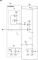
- FIG. It is a circuit diagram which shows the structural example of the pixel 11m, n .
- 3 is a block diagram illustrating a second configuration example of the image sensor 2.
- FIG. 3 is a circuit diagram illustrating details of a second configuration example of the image sensor 2.
- FIG. 6 is a waveform diagram illustrating an example of the operation of the image sensor 2.
- FIG. 5 is a circuit diagram showing details of a third configuration example of the image sensor 2.
- FIG. 6 is a circuit diagram illustrating details of a fourth configuration example of the image sensor 2.
- FIG. 10 is a block diagram illustrating a fifth configuration example of the image sensor 2.
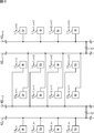
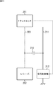
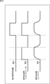
- FIG. It is a block diagram which shows the 6th structural example of the image sensor. It is a block diagram showing an example of composition of a 1st embodiment of a signal transmission system to which this art is applied. It is a wave form diagram explaining the 1st example of operation
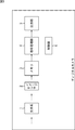
- FIG. 1 is a block diagram illustrating a configuration example of an embodiment of a digital camera to which the present technology is applied.
- the digital camera can capture both still images and moving images.
- the digital camera includes an optical system 1, an image sensor 2, a memory 3, a signal processing unit 4, an output unit 5, and a control unit 6.
- the optical system 1 has, for example, a zoom lens, a focus lens, a diaphragm, and the like (not shown), and makes light from the outside enter the image sensor 2.
- the image sensor 2 is, for example, a CMOS (Complementary Metal Oxide Semiconductor) image sensor that receives incident light from the optical system 1, performs photoelectric conversion, and outputs image data corresponding to the incident light from the optical system 1. To do.
- CMOS Complementary Metal Oxide Semiconductor
- the memory 3 temporarily stores image data output from the image sensor 2.
- the signal processing unit 4 performs processing such as noise removal and white balance adjustment as signal processing using the image data stored in the memory 3 and supplies the processed signal to the output unit 5.
- the output unit 5 outputs the image data from the signal processing unit 4.
- the output unit 5 has a display (not shown) made of, for example, liquid crystal, and displays an image corresponding to the image data from the signal processing unit 4 as a so-called through image.
- the output unit 5 includes a driver (not shown) that drives a recording medium such as a semiconductor memory, a magnetic disk, or an optical disk, and records the image data from the signal processing unit 4 on the recording medium.
- a driver (not shown) that drives a recording medium such as a semiconductor memory, a magnetic disk, or an optical disk, and records the image data from the signal processing unit 4 on the recording medium.
- the output unit 5 has a communication interface, and transmits the image data from the signal processing unit 4 by wireless or wired communication.
- the control unit 6 controls each block constituting the digital camera in accordance with a user operation or the like.
- the image sensor 2 receives incident light from the optical system 1 and outputs image data according to the incident light.
- the image data output from the image sensor 2 is supplied to and stored in the memory 3.
- the image data stored in the memory 3 is subjected to signal processing by the signal processing unit 4, and the resulting image data is supplied to the output unit 5 and output.
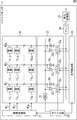
- FIG. 2 is a block diagram showing a first configuration example of the image sensor 2 of FIG.
- the image sensor 2 includes a pixel unit 10, a logic unit 20, a vertical scanning unit 21, a column processing unit 22, a horizontal transfer unit 23, an amplifier 24, a signal processing unit 25, pixel control lines 41 1 to 41 M , and has VSL42 1 through 42 N.
- the pixel unit 10 performs M ⁇ N pixels 11 1 , 1 1 , 11 1 , 2 ,..., 11 1 that perform photoelectric conversion (M and N are integers greater than or equal to 1 (an integer greater than or equal to 1 )).
- N, 11 2,1, 11 2,2 , ⁇ , 11 2, N, ⁇ , 11 M, 1, 11 M, 2, ⁇ , 11 M has a N, image It functions as an imaging unit (imaging device) that captures an image.
- M ⁇ N pixels 11 1,1 to 11 M, N are arranged in a matrix (lattice) of M rows and N columns on a two-dimensional plane.
- n-th column (n 1,2, ⁇ , N ) M pixels 11 1 arranged in the column direction (vertical direction) of, n to 11 M, the n, the column direction An extending VSL 42 n is connected.
- the pixels 11 m and n perform photoelectric conversion of light (incident light) incident thereon. Further, the pixel 11 m, n is connected to the current source 34 n according to the control from the vertical scanning unit 21 via the pixel control line 41 m to the voltage (electric signal) corresponding to the electric charge obtained by photoelectric conversion. Is output on the VSL 42 n .
- the pixels 11 m, n can perform photoelectric conversion of light of a predetermined color that enters through a color filter (not shown) such as a Bayer array.
- Logic unit 20 and the vertical scanning unit 21, the column processing unit 22 (constituting the DAC31 and counter 33 n, etc.), the horizontal transfer unit 23, controlled according to such a predetermined logic.
- the vertical scanning unit 21 under the control of the logic unit 20, via the pixel control line 41 m, to the pixels 11 m, 1 not connected to the pixel control line 41 m 11 m, and controls the N (drive).
- the vertical scanning unit 21 sequentially drives the N pixels 11 m, 1 to 11 m, N in the first to M-th rows of the pixel unit 10 from the first row, and the pixels 11 m in units of rows. , 1 to 11 m, the signal from the N, is output to VSL42 1 to the 42 N.
- the column processing unit 22 is connected to each of N columns of pixels 11 m, 1 to 11 m, N arranged in one row via VSLs 42 1 to 42 N , and thus the pixels 11 m, n are connected to VSL 42 n.
- An electrical signal (voltage) (hereinafter also referred to as a VSL signal) output to the top is supplied to the column processing unit 22.
- the column processing unit 22 performs AD conversion of N VSL signals supplied from the N columns of pixels 11 m, 1 to 11 m, N arranged in one row via the VSLs 42 1 to 42 N in parallel.
- the digital data obtained as a result is supplied to the horizontal transfer unit 23 as pixel values (pixel data) of the pixels 11 m, 1 to 11 m, N.
- the column processing unit 22 performs AD conversion of all the N pixels 11 m, 1 to 11 m, N arranged in one row in parallel, and also performs the N pixels 11 m, 1 to AD conversion of electrical signals of one or more pixels of less than N out of 11 m and N can be performed in parallel.
- the column processing unit 22 performs AD conversion of all VSL signals of N pixels 11 m, 1 to 11 m, N arranged in one row in parallel. .
- the column processing unit 22 includes N comparators 32 1 to 32 N , in order to perform AD conversion of all the VSL signals of N pixels 11 m, 1 to 11 m, N arranged in one row in parallel. , N counters 33 1 to 33 N.
- the column processing unit 22 includes a DAC (Digital to Analog Converter) 31 and N current sources 34 1 to 34 N.
- DAC Digital to Analog Converter
- the DAC 31 performs a DA (Digital to Analog) conversion so that a reference signal having a period in which a level (voltage) changes from a predetermined initial value to a predetermined final value with a constant slope like a ramp signal. Are supplied (output) to the comparators 32 1 to 32 N.
- DA Digital to Analog
- the comparator 32 n is connected to the VSL 41 n . Therefore, the VSL signal (electric signal) output from the pixel 11 m, n on the VSL 41 n is supplied to the comparator 32 n .
- the comparator 32 n compares the VSL signal from the pixel 11 m, n with the reference signal from the DAC 31 and supplies a comparison result signal representing the comparison result to the counter 33 n .
- the counter 33 n is based on the comparison result signal from the comparator 32 n until the level of the VSL signal of the pixel 11 m, n matches the level of the reference signal (the magnitude relationship between the VSL signal and the reference signal is reversed).
- AD Analog to Digital
- CDS Correlated Double Sampling
- a clock is supplied from the logic unit 20 to the counter 33 n .
- the time required for the change in the level of the reference signal until the level of the VSL signal of the pixel 11 m, n matches the level of the reference signal is to count the clock supplied from the logic unit 20. Is done.
- the N comparators 32 1 to 32 N have N pixels in the first to Mth rows of the pixel unit 10.
- the VSL signals of the pixels 11 m, 1 to 11 m, N are sequentially supplied from the first row, for example, and AD conversion and CDS of the VSL signal are performed in units of rows.
- the comparator 32 n and the counter 33 n since the VSL signal is AD-converted as described above, the comparator 32 n and the counter 33 n constitute an ADC (Analog to Digital Converter). It can be said.
- ADC Analog to Digital Converter
- the current source 34 n is connected between the VSL 42 n and the ground, and allows a constant current to flow through the VSL 42 n .
- the current source 34 n constitutes an SF together with an FET 55, which will be described later, constituting the pixel 11m , n, and serves as a load of the SF.
- the horizontal transfer unit 23 performs transfer control in which the count value, that is, digital data as a pixel value is read from the counter 33 n and transferred to the amplifier 24 according to the control of the logic unit 20.
- the amplifier 24 amplifies the pixel value transferred from the counter 33 n and supplies the amplified pixel value to the signal processing unit 25.
- the signal processing unit 25 performs necessary signal processing on the pixel value from the amplifier 24 and outputs it to the outside (in the present embodiment, the memory 3 (FIG. 1)).
- CDS is a signal processing unit 25.
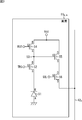
- FIG. 3 is a circuit diagram showing a configuration example of the pixels 11m, n in FIG.
- the pixel 11 m, n includes a PD 51 and four NMOS (negative channel MOS) FETs (Field Effect Transistors) 52, 54, 55, and 56.
- NMOS negative channel MOS
- FETs Field Effect Transistors
- the drain of the FET 52, the source of the FET 54, and the gate of the FET 55 are connected, and an FD (Floating Diffusion) (capacitance) for converting charges into voltage is connected to the connection point. ) 53 is formed.
- FD Floating Diffusion
- PD 51 is an example of a photoelectric conversion element that performs photoelectric conversion, and performs photoelectric conversion by receiving incident light and accumulating charges corresponding to the incident light.
- the anode of the PD 51 is connected (grounded) to the ground, and the cathode of the PD 51 is connected to the source of the FET 52.
- the FET 52 is an FET for transferring the charge accumulated in the PD 51 from the PD 51 to the FD 53, and is also referred to as a transfer Tr 52 hereinafter.
- the source of the transfer Tr 52 is connected to the cathode of the PD 51, and the drain of the transfer Tr 52 is connected to the source of the FET 54 via the FD 53.
- the gate of the transfer Tr52 is connected to the pixel control line 41 m, the gate of the transfer Tr52 via the pixel control line 41 m, the transfer pulse TRG is supplied.
- the vertical scanning unit 21 via a pixel control line 41 m, the pixel 11 m, in order to drive the n (control), the control signal to be supplied to the pixel control line 41 m, the transfer pulse
- TRG the transfer pulse
- RST reset pulse
- SEL selection pulse
- the FD 53 is a region that converts charges into voltage like a capacitor formed at the connection point of the drain of the transfer Tr 52, the source of the FET 54, and the gate of the FET 55.
- the FET 54 is an FET for resetting the electric charge (voltage (potential)) accumulated in the FD 53, and is also referred to as a reset Tr 54 hereinafter.
- the drain of the reset Tr54 is connected to the power supply Vdd.
- the gate of the reset Tr54 is connected to the pixel control line 41 m, the gate of the reset Tr54, via a pixel control line 41 m, the reset pulse RST is supplied.
- the FET 55 is an FET for buffering the voltage of the FD 53, and is hereinafter also referred to as an amplifying Tr 55.
- the gate of the amplification Tr55 is connected to the FD 53, and the drain of the amplification Tr55 is connected to the power supply Vdd.
- the source of the amplifying Tr 55 is connected to the drain of the FET 56.
- the FET 56 is an FET for selecting an output of an electric signal (VSL signal) to the VSL 42 n , and is hereinafter also referred to as a selection Tr 56.
- the source of the selection Tr 56 is connected to the VSL 42 n .
- the gate of the selection Tr56 is connected to the pixel control line 41 m, the gate of the selection Tr56, via a pixel control line 41 m, a selection pulse SEL is supplied.
- the source of the amplifying Tr 55 is connected to the current source 34 n (FIG. 2) via the selection Tr 56 and the VSL 42 n , so that the SF (circuit) is configured by the amplifying Tr 55 and the current source 34 n .
- the FD 53 is connected to the VSL 42 n via the SF.
- pixels 11 m and n can be configured without the selection Tr 56.
- a configuration of a shared pixel in which the FD 53 or the selection Tr 56 is shared by a set of a plurality of PDs 51 and transfer Trs 52 can be employed.
- the PD 51 receives light incident thereon and performs photoelectric conversion to start accumulation of electric charge according to the amount of received incident light.
- the selection pulse SEL is at the H level and the selection Tr 56 is in the ON state.
- the vertical scanning unit 21 (FIG. 2) temporarily transfers the transfer pulse TRG (from the L (Low) level). Set to H (High) level.
- the transfer Tr 52 When the transfer Tr 52 is turned on, the charge accumulated in the PD 51 is transferred to the FD 53 via the transfer Tr 52 and accumulated.
- the vertical scanning unit 21 temporarily sets the reset pulse RST to the H level before temporarily setting the transfer pulse TRG to the H level, and thereby temporarily sets the reset Tr 54 to the ON state.
- the FD 53 When the reset Tr 54 is turned on, the FD 53 is connected to the power supply Vdd via the reset Tr 54, and the charge in the FD 53 is swept out to the power supply Vdd via the reset Tr 54 and reset.
- the vertical scanning unit 21 After the charge of the FD 53 is reset, the vertical scanning unit 21 temporarily sets the transfer pulse TRG to the H level as described above, whereby the transfer Tr 52 is temporarily turned on.
- the transfer Tr 52 When the transfer Tr 52 is turned on, the charge stored in the PD 51 is transferred to the FD 53 after reset via the transfer Tr 52 and stored.
- a voltage (potential) corresponding to the electric charge accumulated in the FD 53 is output as a VSL signal on the VSL 42 n via the amplification Tr 55 and the selection Tr 56.
- the reset level which is a VSL signal immediately after the pixel 11 m, n is reset, is AD-converted.
- a level and a level to be a pixel value are AD-converted.
- the AD conversion result of the reset level (hereinafter also referred to as reset level AD value) and the AD conversion result of the signal level (hereinafter also referred to as signal level AD value).
- CDS for obtaining the difference as a pixel value is performed.
- the CDS is performed by decrementing (or incrementing) the count value in the counter 33 n during AD conversion of the reset level and incrementing (or decrementing) the count value during AD conversion of the signal level. it can.
- FIG. 4 is a block diagram showing a second configuration example of the image sensor 2 of FIG.
- the image sensor 2 includes a pixel unit 10, a logic unit 20, a vertical scanning unit 21, a column processing unit 22, a horizontal transfer unit 23, an amplifier 24, a signal processing unit 25, pixel control lines 41 1 to 41 M , and in that it has a VSL42 1 through 42 N, common to that of FIG.
- the image sensor 2 is different from the case of FIG. 2 in that it has assist VSLs 61 1 to 61 N , signal control units 62 1 to 62 N , and capacitors 63 1 to 63 N.
- Assist VSL61 n is adjacent to VSL42 n (in the form pinch the conductor), a linear conductor as an assist signal lines arranged along the VSL42 n, the capacitance 63 n, VSL42 n capacitively coupled is doing.
- the signal controller 62 n is a similar signal having similarity with the VSL signal flowing to VSL42 n (and VSL signal (almost) the same signal), performs signal control flow to assist VSL61 n.
- the similar signals similar to the VSL signal include the same signal as the VSL signal in addition to the signal similar to the VSL signal.
- the capacitor 63 n is a capacitor that capacitively couples the VSL 42 n and the assist VSL 61 n .
- Capacity 63 n may be a parasitic capacitance between the VSL42 n and the assist VSL61 n, actual capacity, i.e., may be an actual capacitor connected between the VSL42 n and assist VSL61 n .
- the signal control unit 62 n In configured image sensor 2 as described above, the signal control unit 62 n, a similar signal having similarity with the VSL signal flowing in VSL42 n, flow assist VSL61 n.
- the signal control unit 62 n is provided in the column processing unit 22, but the signal control unit 62 n can be provided in the pixel unit 10, for example.
- the signal control unit 62 n can be provided separately for the pixel unit 10 and the column processing unit 22, or can be provided separately from the pixel unit 10 and the column processing unit 22.
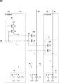
- FIG. 5 is a circuit diagram showing details of the second configuration example of the image sensor 2 of FIG.
- FIG. 5 a part of the image sensor 2 of FIG. 4, that is, the pixel 11 m, n (FD53, amplification Tr55, and selection Tr56), current source 34 n , VSL42 n , assist VSL61 n , , it is shown only the portion of the signal control unit 62 n.
- capacitor 71 is the parasitic capacitance of VSL42 n.
- the signal control unit 62 n includes a signal output unit 81 and a load unit 84.
- the signal output unit 81 has FETs 82 and 83.
- the FET 82 is configured in the same manner as the amplifying Tr 55, the drain is connected to the power supply Vdd, the gate is connected to the FD 53 of the pixels 11 m and n , and the source is connected to the drain of the FET 83.
- FET83 is configured similarly to the selection Tr 56, a drain, a source of FET 82, the gate is the pixel control line 41 n of the selection pulse SEL is supplied, the source, the assist VSL61 n, it is connected.
- the FETs 82 and 83 operate in the same manner as the amplification Tr 55 and the selection Tr 56, respectively.
- the load unit 84 has a current source 85 and a capacitor 86.
- the current source 85 is configured in the same manner as the current source 34 n and allows a constant current to flow through the assist VSL 61 n .
- Current source 85 similar to the current source 34 n, with FET 83, constitutes a SF, which is a load of the SF.
- the capacitor 86 is a parasitic capacitance of the assist VSL 61 n .
- the signal output unit 81 exists for each row of the pixels 11 m and n , and therefore, there are only M signal output units 81. However, in FIG. 5 (the same applies to the drawings described later), the signal output unit 81 in one row is illustrated, and the signal output units in other rows are not illustrated.
- the FETs 82 and 83 operate in the same manner as the amplification Tr 55 and the selection Tr 56.
- VSL42 n and assist VSL61 n which are capacitively coupled by capacitor 63 n, same signal flows.
- FIG. 6 is a waveform diagram for explaining an example of the operation of the image sensor 2 of FIG.
- FIG. 6 shows a signal that the signal output unit 81 passes to the assist VSL 61 n (similar), a source voltage of the amplification Tr 55, and a case A1 in which the signal output unit 81 does not function and a case A2 in which the signal output unit 81 functions. and shows an example of VSL voltage VSL42 n (VSL signal flowing through the VSL42 n).
- Case A2 signal output unit 81 to function when the source voltage of the amplification Tr55 has changed, to the assist VSL61 n, the same signal and VSL signal flowing to VSL42 n (similar signal) flows.
- FIG. 7 is a circuit diagram showing details of the third configuration example of the image sensor 2.
- FIG. 7 shows a part of the image sensor 2 as in FIG.
- the image sensor 2 in FIG. 7 includes a current source 34 n , VSL 42 n , FD 53, amplification Tr 55, selection Tr 56, assist VSL 61 n , signal control unit 62 n , capacitance 63 n , and capacitance 71. Same as the case.
- the image sensor 2 of FIG. 7 is different from the case of FIG. 5 in that the image sensor 2 includes an assist VSL 91 n , a signal control unit 92 n , and a capacitor 93 n .
- Assist VSL91 n like the assist VSL61 n, adjacent (in the form pinch the conductor) to VSL42 n, an assist signal lines arranged along the VSL42 n, the capacitance 93 n, VSL42 n and capacity Are connected.
- Assist VSL61 n and 91 n are assisted VSL61 n is Whereas are wired to the right of VSL42 n, assist VSL91 n is different in that it is wired to the left of VSL42 n.
- the signal controller 92 n like the signal control unit 62 n, a similar signal having similarity with the VSL signal flowing in VSL42 n, performs signal control flow to assist VSL91 n.
- the signal control unit 92 n includes the signal output unit 101 and the load unit 104.
- the signal output unit 101 is configured similarly to the signal output unit 81, and the load unit 104 is configured similarly to the load unit 84.
- the signal processing unit 101 includes FETs 102 and 103 similar to the FETs 82 and 83, respectively, and the FETs 102 and 103 operate in the same manner as the amplification Tr 55 and the selection Tr 56, respectively.
- the load unit 104 includes a current source 105 and a capacitor 106 that are similar to the current source 85 and the capacitor 86, respectively.
- current source 105 similar to the current source 85, supplies a constant current to the assist VSL91 n. Further, like the current source 85, the current source 105 constitutes an SF together with the FET 103, and is a load of the SF.
- the capacitor 106 is the parasitic capacitance of the assist VSL91 n.
- the FETs 82 and 83 operate in the same manner as the amplification Tr55 and the selection Tr56, and the FETs 102 and 103 operate in the same manner as the amplification Tr55 and the selection Tr56.
- an assist VSL61 n bound VSL42 n capacitively by volume 63 n flows the same signal and VSL signal flowing in VSL42 n .
- the right-hand VSL42 n provided with an assist VSL61 n, on the left side of VSL42 n, is provided to assist VSL91 n, Furthermore, for VSL42 n, adjacent to the front side and back side of the drawing Thus, an assist VSL similar to the assist VSL 61 n can be provided.
- FIG. 8 is a circuit diagram showing details of the fourth configuration example of the image sensor 2.
- FIG. 8 a part of the image sensor 2 is illustrated as in FIG.
- the image sensor 2 in FIG. 8 includes a current source 34 n , VSL 42 n , FD 53, amplification Tr 55, selection Tr 56, assist VSL 61 n , signal control unit 62 n , capacitance 63 n , and capacitance 71. Same as the case.
- the assist VSL 61 n is configured by a cylindrical conductor and is wired so as to surround the VSL 42 n , and the assist VSL 61 n is configured by a linear conductor. It is different from the case of.
- the FETs 82 and 83 operate in the same manner as the amplification Tr 55 and the selection Tr 56, and assist the VSL 42 n that is capacitively coupled by the capacitor 63 n . VSL61 to the n, the same signal flows.
- the assist VSL61 n is, are wired so as to surround the VSL42 n, therefore, for VSL42 n, the entire periphery thereof, by the assist VSL61 n, because it is so to speak the shield, FIG. 5 and FIG. As compared with the case of 7, the (bad) influence of the parasitic capacitance 71 of the VSL 42 n can be further reduced.
- FIG. 9 is a block diagram showing a fifth configuration example of the image sensor 2.
- VSLs 42 corresponding to the pixels 11 m, n to 11 m + 3, n + 3 of the 4 rows ⁇ 4 columns with the pixel portion 10 and the pixels 11 m, n to 11 m + 3, n + 3 of the 4 rows 4 columns.
- n to Yes illustrates only 42 n + 3, for the other parts, is not shown.
- FIG. 9 2 rows ⁇ 2 columns of four pixels 11 m, n to 11 m + 1, n + 1 are arrayed in a Bayer array, and the array units are arranged in the horizontal and vertical directions.
- the image sensor 2 in FIG. 9 is configured in the same way as in FIG.
- the upper left pixel 11 m, n receives red light incident through a color filter (not shown), and outputs a signal having a red (R (Red)) pixel value.
- the upper right pixel 11 m, n + 1 and the lower left pixel 11 m + 1, n receive green light incident via a color filter (not shown) and output a signal having a green (G) pixel value.
- the lower right pixel 11 m + 1, n + 1 receives blue light incident through a color filter (not shown) and outputs a signal having a blue (B (Blue)) pixel value.
- R represents an upper left pixel 11m , n that outputs an R signal having a red pixel value in the array unit
- Gr represents a Gr signal having a green pixel value in the array unit.
- This represents the upper right pixel 11 m, n + 1 to be output.
- Gb represents a lower left pixel 11 m + 1, n that outputs a Gb signal that is a green pixel value in an array unit
- B is a lower right that outputs a B signal that is a blue pixel value in the array unit. Represents the pixel 11 m + 1, n + 1 .
- the vertical scanning unit 21 includes the N pixels 11 m and 1 to 11 in each of the first to Mth rows of the pixel unit 10. m and N are sequentially driven from the first row , and signals are output from the pixels 11 m, 1 to 11 m, N to the VSLs 42 1 to 42 N in units of rows.
- FIG. 10 is a block diagram illustrating a sixth configuration example of the image sensor 2.
- FIG. 10 as in the case of FIG. 9, 4 pixels 11 m, n to 11 m + 1, n + 1 of 2 rows ⁇ 2 columns are used as array units of the Bayer array, and the array units are arranged in the horizontal and vertical directions.
- the image sensor 2 of FIG. 10 is common to the case of FIG.
- the image sensor 2 in FIG. 10 pixel 11 1, n to 11 M of a certain row (the n-th column), when attention is paid to the pixel of the n, the pixel 11 1 and the attention, n to 11 M, n and VSL42 n of the target pixel column of, VSL42 n-2 of pixel rows arranged to the left by two rows from the target pixel row, or in that the VSL42 n + 2 pixel rows arranged to the right adjacent, different from the case of FIG. 9 To do.
- VSL42 n of the pixel of interest sequence and to consider the VSL42 n + 2 pixel rows arranged right by two columns from the target pixel column.
- the capacitor C may be a parasitic capacitance between the VSL 42 n and the VSL 42 n + 2 as in the case of the capacitor 63 n in FIG. 4, or may be an actual capacitor.
- the target pixel column is also referred to as a first target pixel column
- a pixel column arranged on the right by two columns from the target pixel column is also referred to as a second target pixel column.
- signals of the same color are output from the pixels in the same row of the first target pixel column and the second target pixel column.
- signals of the same color output from the pixels in the same row of the first target pixel column and the second target pixel column are (substantially) similar signals.
- VSL42 n of the first target pixel row, and the VSL42 n + 2 of the second target pixel columns are adjacent to the wiring, because both are VSL, respectively VSL42 n and 42 n + 2 is , Routed along the other.
- VSLs 42 n and 42 n + 2 are capacitively coupled by the capacitor C.
- VSL42 n is another VSL VSL42 n + 2 is adjacent to VSL42 n, the assist signal lines arranged along the VSL42 n.
- the pixel of the 1st attention pixel row is the pixel of the 1st attention pixel row.
- similar signal having similarity with the VSL signal flowing in VSL42 n, it can be said that flow to VSL42 n + 2. Therefore, a signal control unit that performs signal control for causing the pixels of the second pixel-of-interest column to pass a similar signal similar to the signal flowing through the VSL42 n to the VSL42 n + 2 serving as the assist signal line with respect to the first pixel-of-interest column.
- VSL42 n + 2 which is another VSL VSL42 n is adjacent to VSL42 n + 2, the assist signal lines arranged along the VSL42 n + 2.
- a signal control unit that performs signal control for causing the pixels in the first pixel-of-interest column to flow a similar signal similar to the signal flowing through VSL42 n + 2 to VSL42 n serving as an assist signal line. Function as.
- VSL42 n other VSL42 n + 2, adjacent to VSL42 n, when utilized as an assist signal lines arranged along the VSL42 n, apart from the VSL42 1 through 42 N, Compared with the case of FIGS. 5, 7, and the like in which assist VSLs 61 n and 91 n are provided as assist signal lines, the enlargement of the image sensor 2 can be suppressed.
- the image sensor 2 can be applied to a digital camera, a portable terminal such as a smartphone having a function of capturing an image by mounting the image sensor, and any other electronic device having a function of capturing an image. .
- FIG. 11 is a block diagram illustrating a configuration example of the first embodiment of the signal transmission system to which the present technology is applied.
- the method for reducing the adverse effect of the parasitic capacitance can be applied to a signal transmission system that transmits a signal through a wired transmission path in addition to the image sensor 2.
- FIG. 11 shows a configuration example of the first embodiment of such a signal transmission system.
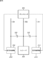
- the signal transmission system includes a transmitter 201, a receiver 202, a signal transmission path 203, an assist transmission path 211, a signal control unit 212, and a capacitor 213.
- the transmitter 201 outputs, for example, a transmission signal suitable for transmission through the signal transmission path 203 to the signal transmission path 203, thereby transmitting (transmitting) the transmission signal via the signal transmission path 203.
- the receiver 202 receives a transmission signal transmitted from the transmitter 202 and flowing through the signal transmission path 203.
- the signal transmission path 203 is a wired transmission path, and a transmission signal output from the transmitter 201 flows through the signal transmission path 203.
- the assist transmission path 211 is a wired transmission path that is adjacent to the signal transmission path 203 and wired along the signal transmission path 203.
- the signal control unit 212 monitors the transmitter 201 and performs signal control to flow a similar signal similar to the transmission signal output from the transmitter 201 to the signal transmission path 203 through the assist transmission path 211.
- the capacity 213 is a capacity for capacitively coupling the signal transmission path 203 and the assist transmission path 211.
- the capacitor 213 may be a parasitic capacitance between the signal transmission path 203 and the assist transmission path 211 or may be an actual capacity.
- the signal control unit 212 monitors the transmitter 201, and transmits a similar signal similar to the transmission signal that the transmitter 201 sends to the signal transmission path 203 by the capacitor 213. It flows through the assist transmission path 211 that is capacitively coupled to the path 203.
- the (bad) influence of the parasitic capacitance of the signal transmission path 203 can be easily reduced without signal feedback. It is possible to suppress degradation of signal quality of a transmission signal flowing through the signal transmission path 203 due to the capacity.
- FIG. 12 is a waveform diagram for explaining a first example of the operation of the signal transmission system of FIG.
- FIG. 12 shows an example of the operation of the signal transmission system when the signal control unit 212 is not functioned.
- the waveform of the signal W11 that flows in another signal transmission path that is not capacitively coupled to the signal transmission path 203, the waveform of the transmission signal W12 that the transmitter 201 outputs to the signal transmission path 203, and the signal that is received by the receiver 202 An example of the waveform of the reception signal W13 obtained by receiving the transmission signal W12 flowing through the transmission path 203 is shown.
- the transmission signal W12 flowing through the signal transmission path 203 is affected by the parasitic capacitance of the signal transmission path 203 regardless of the signal W11 flowing through the other signal transmission paths.
- the reception signal W13 is Compared with W12, the signal quality is greatly deteriorated (signal with a greatly reduced slew rate).
- FIG. 13 is a waveform diagram for explaining a second example of the operation of the signal transmission system of FIG.
- FIG. 13 shows an example of the operation of the signal transmission system when the signal control unit 212 is caused to function.
- the waveform of the similar signal W21 that flows in the assist transmission path 211 that is capacitively coupled to the signal transmission path 203 by the capacitor 213, the waveform of the transmission signal W22 that the transmitter 201 outputs to the signal transmission path 203, and the receiver 202 Shows an example of the waveform of the reception signal W23 obtained by receiving the transmission signal W22 flowing through the signal transmission path 203.
- a similar signal W21 that is similar to the transmission signal W22 that flows through the signal transmission path 203 flows through the assist transmission path 211 that is capacitively coupled by the signal transmission path 203 and the capacitor 213, thereby causing the signal transmission path 203 to The effect of parasitic capacitance is reduced.
- the received signal W23 is a signal in which deterioration of the signal quality is suppressed, that is, for example, a signal in which a decrease in the slew rate is suppressed as compared with the received signal W13 in FIG.
- FIG. 14 is a block diagram illustrating a configuration example of the second embodiment of the signal transmission system to which the present technology is applied.
- FIG. 14 portions corresponding to those in FIG. 11 are denoted by the same reference numerals, and description thereof will be omitted below as appropriate.
- the signal transmission system of FIG. 14 is common to the case of FIG. 11 in that it includes a transmitter 201, a receiver 202, a signal transmission path 203, a signal control unit 212, and a capacitor 213.
- the signal transmission system of FIG. 14 differs from the case of FIG. 11 in that an assist transmission path 221 is provided instead of the assist transmission path 211.
- the assist transmission path 211 in FIG. 11 is a (straight) linear conductor (transmission path), whereas the assist transmission path 221 in FIG. 14 is a cylindrical conductor and surrounds the signal transmission path 203. Is different from the case of FIG.
- FIG. 15 is a block diagram illustrating a configuration example of the third embodiment of the signal transmission system to which the present technology is applied.
- FIG. 15 portions corresponding to those in FIG. 11 are denoted by the same reference numerals, and description thereof will be omitted below as appropriate.
- the signal transmission system of FIG. 15 is common to the case of FIG. 11 in that it includes a transmitter 201, a receiver 202, and a signal transmission path 203.
- the signal transmission system of FIG. 15 is not provided with the assist transmission path 211, the signal control unit 212, and the capacitor 213, but has a transmitter 231, a receiver 232, a signal transmission path 233, and a capacitor 241. This is different from the case of FIG.
- the transmitter 231, the receiver 232, and the signal transmission path 233 are configured in the same manner as the transmitter 201, the receiver 202, and the signal transmission path 203, respectively.
- the transmitter 231 outputs the transmission signal to the signal transmission path 233, thereby transmitting (transmitting) the transmission signal via the signal transmission path 233.
- the receiver 232 receives a transmission signal transmitted from the transmitter 232 and flowing through the signal transmission path 233.
- the signal transmission paths 203 and 233 are adjacent to the other and wired along the other.
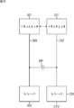
- the capacitor 241 is a capacitor that capacitively couples the signal transmission paths 203 and 233.
- the capacitor 213 may be a parasitic capacitor between the signal transmission paths 203 and 233, or may be an actual capacitor.
- the transmitters 201 and 231 output similar signals that are similar to each other, such as the same signal, for example, as transmission signals.
- the same signal flows through the signal transmission lines 203 and 233 that are capacitively coupled by the capacitor 241.
- the (bad) influence of the parasitic capacitance of the signal transmission path 203 and the parasitic capacitance of the signal transmission path 233 is reduced, and the receiver 202 causes the parasitic capacitance of the signal transmission path 203 via the signal transmission path 203. It is possible to suppress the deterioration of the quality of the transmission signal received and to suppress the deterioration of the quality of the transmission signal received via the signal transmission path 233 by the receiver 232 due to the parasitic capacitance of the signal transmission path 233. .
- the signal transmission path 233 which is another signal transmission path, is adjacent to the signal transmission path 203 and becomes an assist transmission path wired along the signal transmission path 203.
- the transmitter 231 since the same transmission signal is output from the transmitter 201 and the transmitter 231, the transmitter 231 transmits a similar signal similar to the transmission signal that the transmitter 201 sends to the signal transmission path 203 to the signal transmission path. 233 can be said to flow. Therefore, for the transmitter 201, the transmitter 231 functions as a signal control unit that performs signal control for flowing a similar signal similar to the signal flowing in the signal transmission path 203 to the signal transmission path 233 as the assist transmission path.
- the signal transmission path 203 which is another signal transmission path, is adjacent to the signal transmission path 233 and becomes an assist transmission path wired along the signal transmission path 233.
- the transmitter 201 since the same transmission signal is output from the transmitter 201 and the transmitter 231, the transmitter 201 transmits a similar signal similar to the transmission signal that the transmitter 231 sends to the signal transmission path 233 to the signal transmission path. It can be said that it flows to 203. Therefore, for the transmitter 231, the transmitter 201 functions as a signal control unit that performs signal control for causing a similar signal similar to the signal flowing in the signal transmission path 233 to flow in the signal transmission path 203 as the assist transmission path.
- the transmitters 201 and 231 can be replaced with one transmitter.
- the receivers 202 and 232 can be replaced with one receiver.
- FIG. 16 is a block diagram illustrating a configuration example of the fourth embodiment of the signal transmission system to which the present technology is applied.
- FIG. 16 portions corresponding to those in FIG. 11 are denoted by the same reference numerals, and description thereof will be omitted below as appropriate.
- the signal transmission system of FIG. 16 is common to the case of FIG. 11 in that it includes a transmitter 201, a receiver 202, a signal transmission path 203, an assist transmission path 211, a signal control unit 212, and a capacitor 213.
- the signal transmission system of FIG. 16 is different from the case of FIG. 11 in that it has an assist transmission path 251, a signal control unit 252, and a capacity 253.
- Assist transmission path 251, signal control unit 252, and capacity 253 are configured in the same manner as assist transmission path 211, signal control section 212, and capacity 213, respectively.
- the assist transmission path 251 is adjacent to the signal transmission path 203 and wired along the signal transmission path 203.
- the assist transmission path 211 is wired to the right of the signal transmission path 203, but the assist transmission path 251 is wired to the left of the signal transmission path 203.
- the signal control unit 252 monitors the transmitter 201 and performs signal control to flow a similar signal similar to the transmission signal output from the transmitter 201 to the signal transmission path 203 through the assist transmission path 251.
- the capacity 253 is a capacity for capacitively coupling the signal transmission path 203 and the assist transmission path 251.
- the capacitor 253 may be a parasitic capacitance between the signal transmission path 203 and the assist transmission path 251 or may be an actual capacity.
- the assist transmission path 211 that is capacitively coupled to the signal transmission path 203 by the capacitor 213, and the assist transmission path 251 that is capacitively coupled to the signal transmission path 203 by the capacitance 253;
- the (bad) influence of the parasitic capacitance of the signal transmission path 203 is further reduced, and the quality of the transmission signal received by the receiver 202 via the signal transmission path 203 due to the parasitic capacitance of the signal transmission path 203 is reduced. Deterioration can be suppressed.
- the assist transmission path 211 is provided on the right side of the signal transmission path 203 and the assist transmission path 251 is provided on the left side of the signal transmission path 203, but for the signal transmission path 203, An assist transmission path similar to the assist transmission path 211 can be provided so as to be adjacent to the front side or the back side of the drawing.
- FIG. 17 is a block diagram illustrating a configuration example of the fifth embodiment of the signal transmission system to which the present technology is applied.
- FIG. 17 portions corresponding to those in FIG. 11 are denoted by the same reference numerals, and description thereof will be omitted below as appropriate.
- the signal transmission system of FIG. 17 is common to the case of FIG. 11 in that it includes a transmitter 201, a receiver 202, a signal transmission path 203, an assist transmission path 211, a signal control unit 212, and a capacitor 213.
- the signal transmission system of FIG. 17 is different from the case of FIG. 11 in that it has a signal transmission path 204, an assist transmission path 271, a signal control unit 272, and a capacitor 273.
- the signal transmission path 204 is configured in the same manner as the signal transmission path 203. A transmission signal output from the transmitter 201 flows through the signal transmission path 204.
- the transmitter 201 can transmit a transmission signal to the receiver 202 via any of the signal transmission paths 203 and 204.
- the transmission signal transmitted by the transmitter 201 via the signal transmission path 203 and the transmission signal transmitted via the signal transmission path 204 may be the same signal or different signals.
- Assist transmission path 271, signal control unit 272, and capacity 273 are configured in the same manner as assist transmission path 211, signal control section 212, and capacity 213, respectively.
- the assist transmission path 271 is adjacent to the signal transmission path 204 and wired along the signal transmission path 204.
- the signal control unit 272 monitors the transmitter 201 and performs signal control to flow a similar signal similar to the transmission signal output from the transmitter 201 to the signal transmission path 204 through the assist transmission path 271.
- the capacity 273 is a capacity for capacitively coupling the signal transmission path 204 and the assist transmission path 271.
- the capacitor 273 may be a parasitic capacitance between the signal transmission path 204 and the assist transmission path 271 or may be an actual capacity.
- the signal control unit 212 monitors the transmitter 201, and transmits a similar signal similar to the transmission signal that the transmitter 201 sends to the signal transmission path 203 with a capacity.
- the signal is sent to the assist transmission line 211 that is capacitively coupled to the signal transmission line 203 by 213.
- the (bad) influence of the parasitic capacitance of the signal transmission path 203 can be easily reduced without signal feedback. It is possible to suppress degradation of signal quality of a transmission signal flowing through the signal transmission path 203 due to the capacity.
- the signal control unit 272 monitors the transmitter 201, and transmits a similar signal similar to the transmission signal that the transmitter 201 sends to the signal transmission path 204 by the capacitor 273.
- the data is sent to the assist transmission path 271 that is capacitively coupled to the H.204.
- the (bad) influence of the parasitic capacitance of the signal transmission path 204 can be easily reduced without signal feedback due to the equipotential. It is possible to suppress deterioration in signal quality of a transmission signal flowing through the signal transmission path 204 due to the capacity.
- the system means a set of a plurality of components (devices, modules (parts), etc.), and it does not matter whether all the components are in the same housing. Accordingly, a plurality of devices housed in separate housings and connected via a network and a single device housing a plurality of modules in one housing are all systems. .
- this technique can take the following structures.
- VSL Very Signal Line
- An assist signal line adjacent to the VSL and routed along the VSL;
- An image sensor comprising: a signal control unit configured to flow a similar signal similar to a signal flowing through the VSL to the assist signal line.
- the image sensor according to ⁇ 1> including a plurality of the VSLs.
- the assist signal line is wired so as to be capacitively coupled to the VSL.
- the assist signal line and the VSL are capacitively coupled by a parasitic capacitance.
- ⁇ 5> The image sensor according to any one of ⁇ 1> to ⁇ 4>, wherein a plurality of the assist signal lines are wired to one VSL.
- ⁇ 6> The image sensor according to any one of ⁇ 1> to ⁇ 4>, wherein the assist signal line is wired so as to surround the VSL.
- ⁇ 7> The image sensor according to any one of ⁇ 1> to ⁇ 4>, wherein the assist signal line is another VSL in which a signal having the same color as the signal flowing in the VSL flows.
- An optical system that collects the light;
- An image sensor that receives light and captures an image, The image sensor is VSL (Vertical Signal Line) through which the signal output from the pixel flows, An assist signal line adjacent to the VSL and routed along the VSL;
- An electronic device comprising: a signal control unit configured to flow a similar signal similar to a signal flowing through the VSL to the assist signal line.
- a signal transmission system comprising: a signal control unit that causes a similar signal similar to a signal flowing in the signal transmission path to flow in the assist transmission path.
- ⁇ 12> The signal transmission system according to ⁇ 11>, including a plurality of the signal transmission paths.
- ⁇ 13> The signal transmission system according to ⁇ 11> or ⁇ 12>, wherein the assist transmission path is wired to be capacitively coupled to the signal transmission path.
- ⁇ 14> The signal transmission system according to ⁇ 13>, wherein the assist transmission path and the signal transmission path are capacitively coupled by a parasitic capacitance.
- ⁇ 16> The signal transmission system according to any one of ⁇ 11> to ⁇ 14>, wherein the assist transmission path is wired so as to surround the signal transmission path.
- the assist transmission path is another signal transmission path.
Landscapes
- Engineering & Computer Science (AREA)
- Multimedia (AREA)
- Signal Processing (AREA)
- Transforming Light Signals Into Electric Signals (AREA)
- Solid State Image Pick-Up Elements (AREA)
Abstract
Description
画素が出力する信号が流れるVSL(Vertical Signal Line)と、
前記VSLに隣接し、前記VSLに沿って配線されたアシスト信号線と、
前記VSLに流れる信号と類似性のある類似信号を、前記アシスト信号線に流す信号制御部と
を含むイメージセンサ。
<2>
複数の前記VSLを含む
<1>に記載のイメージセンサ。
<3>
前記アシスト信号線は、前記VSLと容量結合するように配線されている
<1>又は<2>に記載のイメージセンサ。
<4>
前記アシスト信号線と、前記VSLとは、寄生容量によって容量結合している
<3>に記載のイメージセンサ。
<5>
1本の前記VSLに対して、複数本の前記アシスト信号線が配線されている
<1>ないし<4>のいずれかに記載のイメージセンサ。
<6>
前記アシスト信号線は、前記VSLを囲むように配線されている
<1>ないし<4>のいずれかに記載のイメージセンサ。
<7>
前記アシスト信号線は、前記VSLに流れる信号と同一色の信号が流れる他のVSLである
<1>ないし<4>のいずれかに記載のイメージセンサ。
<8>
ベイヤ配列の画素が出力する信号が流れる前記VSLの前記アシスト信号線は、前記画素から2列だけ左又は右に並ぶ画素が出力する信号が流れるVSLである
<7>に記載のイメージセンサ。
<9>
画素が出力する信号が流れるVSL(Vertical Signal Line)と、
前記VSLに隣接し、前記VSLに沿って配線されたアシスト信号線と
を有するイメージセンサが、
前記VSLに流れる信号と類似性のある類似信号を、前記アシスト信号線に流す
制御方法。
<10>
光を集光する光学系と、
光を受光し、画像を撮像するイメージセンサと
を含み、
前記イメージセンサは、
画素が出力する信号が流れるVSL(Vertical Signal Line)と、
前記VSLに隣接し、前記VSLに沿って配線されたアシスト信号線と、
前記VSLに流れる信号と類似性のある類似信号を、前記アシスト信号線に流す信号制御部と
を含む
電子機器。
<11>
トランスミッタが出力する信号が流れる有線の信号伝送路に隣接し、前記信号伝送路に沿って配線された有線のアシスト伝送路と、
前記信号伝送路に流れる信号と類似性のある類似信号を、前記アシスト伝送路に流す信号制御部と
を含む信号伝送システム。
<12>
複数の前記信号伝送路を含む
<11>に記載の信号伝送システム。
<13>
前記アシスト伝送路は、前記信号伝送路と容量結合するように配線されている
<11>又は<12>に記載の信号伝送システム。
<14>
前記アシスト伝送路と、前記信号伝送路とは、寄生容量によって容量結合している
<13>に記載の信号伝送システム。
<15>
1本の前記信号伝送路に対して、複数本の前記アシスト伝送路が配線されている
<11>ないし<14>のいずれかに記載の信号伝送システム。
<16>
前記アシスト伝送路は、前記信号伝送路を囲むように配線されている
<11>ないし<14>のいずれかに記載の信号伝送システム。
<17>
前記アシスト伝送路は、他の信号伝送路である
<11>ないし<14>のいずれかに記載の信号伝送システム。
<18>
トランスミッタが出力する信号が流れる信号伝送路に隣接し、前記信号伝送路に沿って配線されたアシスト伝送路を有する信号伝送システムが、
前記信号伝送路に流れる信号と類似性のある類似信号を、前記アシスト伝送路に流す
制御方法。
Claims (18)
- 画素が出力する信号が流れるVSL(Vertical Signal Line)と、
前記VSLに隣接し、前記VSLに沿って配線されたアシスト信号線と、
前記VSLに流れる信号と類似性のある類似信号を、前記アシスト信号線に流す信号制御部と
を含むイメージセンサ。 - 複数の前記VSLを含む
請求項1に記載のイメージセンサ。 - 前記アシスト信号線は、前記VSLと容量結合するように配線されている
請求項2に記載のイメージセンサ。 - 前記アシスト信号線と、前記VSLとは、寄生容量によって容量結合している
請求項3に記載のイメージセンサ。 - 1本の前記VSLに対して、複数本の前記アシスト信号線が配線されている
請求項3に記載のイメージセンサ。 - 前記アシスト信号線は、前記VSLを囲むように配線されている
請求項3に記載のイメージセンサ。 - 前記アシスト信号線は、前記VSLに流れる信号と同一色の信号が流れる他のVSLである
請求項3に記載のイメージセンサ。 - ベイヤ配列の画素が出力する信号が流れる前記VSLの前記アシスト信号線は、前記画素から2列だけ左又は右に並ぶ画素が出力する信号が流れるVSLである
請求項7に記載のイメージセンサ。 - 画素が出力する信号が流れるVSL(Vertical Signal Line)と、
前記VSLに隣接し、前記VSLに沿って配線されたアシスト信号線と
を有するイメージセンサが、
前記VSLに流れる信号と類似性のある類似信号を、前記アシスト信号線に流す
制御方法。 - 光を集光する光学系と、
光を受光し、画像を撮像するイメージセンサと
を含み、
前記イメージセンサは、
画素が出力する信号が流れるVSL(Vertical Signal Line)と、
前記VSLに隣接し、前記VSLに沿って配線されたアシスト信号線と、
前記VSLに流れる信号と類似性のある類似信号を、前記アシスト信号線に流す信号制御部と
を含む
電子機器。 - トランスミッタが出力する信号が流れる有線の信号伝送路に隣接し、前記信号伝送路に沿って配線された有線のアシスト伝送路と、
前記信号伝送路に流れる信号と類似性のある類似信号を、前記アシスト伝送路に流す信号制御部と
を含む信号伝送システム。 - 複数の前記信号伝送路を含む
請求項11に記載の信号伝送システム。 - 前記アシスト伝送路は、前記信号伝送路と容量結合するように配線されている
請求項12に記載の信号伝送システム。 - 前記アシスト伝送路と、前記信号伝送路とは、寄生容量によって容量結合している
請求項13に記載の信号伝送システム。 - 1本の前記信号伝送路に対して、複数本の前記アシスト伝送路が配線されている
請求項13に記載の信号伝送システム。 - 前記アシスト伝送路は、前記信号伝送路を囲むように配線されている
請求項13に記載の信号伝送システム。 - 前記アシスト伝送路は、他の信号伝送路である
請求項13に記載の信号伝送システム。 - トランスミッタが出力する信号が流れる信号伝送路に隣接し、前記信号伝送路に沿って配線されたアシスト伝送路を有する信号伝送システムが、
前記信号伝送路に流れる信号と類似性のある類似信号を、前記アシスト伝送路に流す
制御方法。
Priority Applications (2)
| Application Number | Priority Date | Filing Date | Title |
|---|---|---|---|
| US15/327,443 US10477123B2 (en) | 2014-07-29 | 2015-07-17 | Image sensor, electronic apparatus, signal transmission system, and control method |
| JP2016538271A JP6702869B2 (ja) | 2014-07-29 | 2015-07-17 | イメージセンサ、電子機器、及び、制御方法 |
Applications Claiming Priority (2)
| Application Number | Priority Date | Filing Date | Title |
|---|---|---|---|
| JP2014153561 | 2014-07-29 | ||
| JP2014-153561 | 2014-07-29 |
Publications (1)
| Publication Number | Publication Date |
|---|---|
| WO2016017449A1 true WO2016017449A1 (ja) | 2016-02-04 |
Family
ID=55217354
Family Applications (1)
| Application Number | Title | Priority Date | Filing Date |
|---|---|---|---|
| PCT/JP2015/070496 Ceased WO2016017449A1 (ja) | 2014-07-29 | 2015-07-17 | イメージセンサ、電子機器、信号伝送システム、及び、制御方法 |
Country Status (3)
| Country | Link |
|---|---|
| US (1) | US10477123B2 (ja) |
| JP (1) | JP6702869B2 (ja) |
| WO (1) | WO2016017449A1 (ja) |
Families Citing this family (4)
| Publication number | Priority date | Publication date | Assignee | Title |
|---|---|---|---|---|
| EP3253047B1 (en) * | 2015-01-28 | 2018-11-28 | Panasonic Intellectual Property Management Co., Ltd. | Solid-state imaging device and camera |
| WO2017159122A1 (ja) * | 2016-03-16 | 2017-09-21 | 株式会社リコー | 光電変換装置、画像読取装置及び画像形成装置 |
| US11363229B1 (en) * | 2021-04-27 | 2022-06-14 | Innolux Corporation | Electronic device |
| JP2024118055A (ja) * | 2023-02-20 | 2024-08-30 | キヤノン株式会社 | 光電変換装置及び光電変換システム |
Citations (3)
| Publication number | Priority date | Publication date | Assignee | Title |
|---|---|---|---|---|
| JP2010098516A (ja) * | 2008-10-16 | 2010-04-30 | Sony Corp | 撮像素子およびその制御方法並びにカメラ |
| JP2011114843A (ja) * | 2009-11-30 | 2011-06-09 | Toshiba Corp | 固体撮像装置 |
| JP2013501482A (ja) * | 2009-08-03 | 2013-01-10 | テキサス インスツルメンツ インコーポレイテッド | 3相モードのofdm伝送方法 |
Family Cites Families (7)
| Publication number | Priority date | Publication date | Assignee | Title |
|---|---|---|---|---|
| JP2007300521A (ja) * | 2006-05-02 | 2007-11-15 | Olympus Corp | 固体撮像装置 |
| US8094223B1 (en) * | 2007-05-30 | 2012-01-10 | On Semiconductor Trading Ltd. | Bus driving in an image sensor |
| US20110017604A1 (en) * | 2008-04-23 | 2011-01-27 | Atomic Energy Council - Institute Of Nuclear Energy Research | Method for making semiconductor electrodes |
| KR20110061677A (ko) * | 2009-12-02 | 2011-06-10 | 삼성전자주식회사 | 영상 센서 및 이의 제조 방법. |
| KR20110085768A (ko) * | 2010-01-21 | 2011-07-27 | 삼성전자주식회사 | Cmos 이미지 센서, 상기 이미지 센서의 데이터 리드아웃 방법, 및 상기 이미지 센서를 포함하는 전자 시스템 |
| JP5521745B2 (ja) | 2010-04-28 | 2014-06-18 | ソニー株式会社 | 固体撮像素子およびその駆動方法、並びにカメラシステム |
| JP6149572B2 (ja) * | 2013-07-25 | 2017-06-21 | ソニー株式会社 | イメージセンサ、制御方法、及び、電子機器 |
-
2015
- 2015-07-17 US US15/327,443 patent/US10477123B2/en active Active
- 2015-07-17 WO PCT/JP2015/070496 patent/WO2016017449A1/ja not_active Ceased
- 2015-07-17 JP JP2016538271A patent/JP6702869B2/ja not_active Expired - Fee Related
Patent Citations (3)
| Publication number | Priority date | Publication date | Assignee | Title |
|---|---|---|---|---|
| JP2010098516A (ja) * | 2008-10-16 | 2010-04-30 | Sony Corp | 撮像素子およびその制御方法並びにカメラ |
| JP2013501482A (ja) * | 2009-08-03 | 2013-01-10 | テキサス インスツルメンツ インコーポレイテッド | 3相モードのofdm伝送方法 |
| JP2011114843A (ja) * | 2009-11-30 | 2011-06-09 | Toshiba Corp | 固体撮像装置 |
Also Published As
| Publication number | Publication date |
|---|---|
| US10477123B2 (en) | 2019-11-12 |
| JPWO2016017449A1 (ja) | 2017-04-27 |
| US20170180655A1 (en) | 2017-06-22 |
| JP6702869B2 (ja) | 2020-06-03 |
Similar Documents
| Publication | Publication Date | Title |
|---|---|---|
| TWI726070B (zh) | 固體攝像元件 | |
| US10070103B2 (en) | Solid-state imaging device, driving method, and electronic device | |
| CN110771155B (zh) | 固态摄像装置、固态摄像装置的驱动方法、以及电子设备 | |
| JP4054839B1 (ja) | 光電変換装置およびそれを用いた撮像システム | |
| US9041583B2 (en) | Comparator, solid-state imaging device, electronic apparatus, and driving method | |
| US9029752B2 (en) | Solid state imaging apparatus including reference signal generator with a slope converting circuit | |
| CN103581581B (zh) | 固态成像器件以及制造方法 | |
| US9264637B2 (en) | Solid-state image pickup apparatus | |
| US9906746B2 (en) | Solid-state image pickup device and image pickup apparatus | |
| KR102553988B1 (ko) | 고체 촬상 소자 및 촬상 장치 | |
| US20100097510A1 (en) | Image pickup element and control method therefor, and camera | |
| CN105578086B (zh) | 光电转换装置以及摄像系统 | |
| US9294698B2 (en) | Solid-state image pickup apparatus | |
| JP2015233184A (ja) | イメージセンサ、電子機器、コンパレータ、及び、駆動方法 | |
| KR20160040173A (ko) | 변환 장치, 촬상 장치, 전자 기기, 변환 방법 | |
| US11095841B2 (en) | Imaging apparatus, imaging system, and driving method for imaging apparatus having capability of reducing deterioration of accuracy of A/D conversion | |
| CN103002231A (zh) | 固态图像拾取器件和相机系统 | |
| US9571771B2 (en) | Data transfer circuit, imaging device and imaging apparatus | |
| US20160142661A1 (en) | Solid-state imaging device and camera | |
| US20190260955A1 (en) | Pixel output level control device and cmos image sensor using the same | |
| JP6702869B2 (ja) | イメージセンサ、電子機器、及び、制御方法 | |
| CN103379292B (zh) | 信号处理设备及方法、成像设备和固态成像元件 | |
| CN102164251B (zh) | 图像传感器的信号处理电路及信号处理方法 | |
| JP4666383B2 (ja) | 増幅型固体撮像装置および電子情報機器 | |
| US10397501B2 (en) | Solid-state image sensor and imaging apparatus |
Legal Events
| Date | Code | Title | Description |
|---|---|---|---|
| 121 | Ep: the epo has been informed by wipo that ep was designated in this application |
Ref document number: 15828128 Country of ref document: EP Kind code of ref document: A1 |
|
| ENP | Entry into the national phase |
Ref document number: 2016538271 Country of ref document: JP Kind code of ref document: A |
|
| WWE | Wipo information: entry into national phase |
Ref document number: 15327443 Country of ref document: US |
|
| NENP | Non-entry into the national phase |
Ref country code: DE |
|
| 122 | Ep: pct application non-entry in european phase |
Ref document number: 15828128 Country of ref document: EP Kind code of ref document: A1 |