WO2016017433A1 - 光レセプタクルおよび光モジュール - Google Patents
光レセプタクルおよび光モジュール Download PDFInfo
- Publication number
- WO2016017433A1 WO2016017433A1 PCT/JP2015/070351 JP2015070351W WO2016017433A1 WO 2016017433 A1 WO2016017433 A1 WO 2016017433A1 JP 2015070351 W JP2015070351 W JP 2015070351W WO 2016017433 A1 WO2016017433 A1 WO 2016017433A1
- Authority
- WO
- WIPO (PCT)
- Prior art keywords
- optical
- substrate
- photoelectric conversion
- receptacle
- light
- Prior art date
- Legal status (The legal status is an assumption and is not a legal conclusion. Google has not performed a legal analysis and makes no representation as to the accuracy of the status listed.)
- Ceased
Links
Images



Classifications
-
- G—PHYSICS
- G02—OPTICS
- G02B—OPTICAL ELEMENTS, SYSTEMS OR APPARATUS
- G02B6/00—Light guides; Structural details of arrangements comprising light guides and other optical elements, e.g. couplings
- G02B6/24—Coupling light guides
- G02B6/42—Coupling light guides with opto-electronic elements
- G02B6/4201—Packages, e.g. shape, construction, internal or external details
- G02B6/4219—Mechanical fixtures for holding or positioning the elements relative to each other in the couplings; Alignment methods for the elements, e.g. measuring or observing methods especially used therefor
- G02B6/4236—Fixing or mounting methods of the aligned elements
- G02B6/4239—Adhesive bonding; Encapsulation with polymer material
-
- G—PHYSICS
- G02—OPTICS
- G02B—OPTICAL ELEMENTS, SYSTEMS OR APPARATUS
- G02B6/00—Light guides; Structural details of arrangements comprising light guides and other optical elements, e.g. couplings
- G02B6/24—Coupling light guides
- G02B6/42—Coupling light guides with opto-electronic elements
- G02B6/4201—Packages, e.g. shape, construction, internal or external details
- G02B6/4204—Packages, e.g. shape, construction, internal or external details the coupling comprising intermediate optical elements, e.g. lenses, holograms
- G02B6/4214—Packages, e.g. shape, construction, internal or external details the coupling comprising intermediate optical elements, e.g. lenses, holograms the intermediate optical element having redirecting reflective means, e.g. mirrors, prisms for deflecting the radiation from horizontal to down- or upward direction toward a device
-
- G—PHYSICS
- G02—OPTICS
- G02B—OPTICAL ELEMENTS, SYSTEMS OR APPARATUS
- G02B6/00—Light guides; Structural details of arrangements comprising light guides and other optical elements, e.g. couplings
- G02B6/24—Coupling light guides
- G02B6/42—Coupling light guides with opto-electronic elements
- G02B6/4201—Packages, e.g. shape, construction, internal or external details
- G02B6/4219—Mechanical fixtures for holding or positioning the elements relative to each other in the couplings; Alignment methods for the elements, e.g. measuring or observing methods especially used therefor
- G02B6/4228—Passive alignment, i.e. without a detection of the degree of coupling or the position of the elements
- G02B6/423—Passive alignment, i.e. without a detection of the degree of coupling or the position of the elements using guiding surfaces for the alignment
-
- G—PHYSICS
- G02—OPTICS
- G02B—OPTICAL ELEMENTS, SYSTEMS OR APPARATUS
- G02B6/00—Light guides; Structural details of arrangements comprising light guides and other optical elements, e.g. couplings
- G02B6/24—Coupling light guides
- G02B6/42—Coupling light guides with opto-electronic elements
- G02B6/4201—Packages, e.g. shape, construction, internal or external details
- G02B6/4219—Mechanical fixtures for holding or positioning the elements relative to each other in the couplings; Alignment methods for the elements, e.g. measuring or observing methods especially used therefor
- G02B6/4236—Fixing or mounting methods of the aligned elements
- G02B6/4244—Mounting of the optical elements
-
- G—PHYSICS
- G02—OPTICS
- G02B—OPTICAL ELEMENTS, SYSTEMS OR APPARATUS
- G02B6/00—Light guides; Structural details of arrangements comprising light guides and other optical elements, e.g. couplings
- G02B6/24—Coupling light guides
- G02B6/42—Coupling light guides with opto-electronic elements
- G02B6/4201—Packages, e.g. shape, construction, internal or external details
- G02B6/4249—Packages, e.g. shape, construction, internal or external details comprising arrays of active devices and fibres
-
- G—PHYSICS
- G02—OPTICS
- G02B—OPTICAL ELEMENTS, SYSTEMS OR APPARATUS
- G02B6/00—Light guides; Structural details of arrangements comprising light guides and other optical elements, e.g. couplings
- G02B6/24—Coupling light guides
- G02B6/42—Coupling light guides with opto-electronic elements
- G02B6/4201—Packages, e.g. shape, construction, internal or external details
- G02B6/4256—Details of housings
- G02B6/4257—Details of housings having a supporting carrier or a mounting substrate or a mounting plate
-
- G—PHYSICS
- G02—OPTICS
- G02B—OPTICAL ELEMENTS, SYSTEMS OR APPARATUS
- G02B6/00—Light guides; Structural details of arrangements comprising light guides and other optical elements, e.g. couplings
- G02B6/24—Coupling light guides
- G02B6/42—Coupling light guides with opto-electronic elements
- G02B6/4292—Coupling light guides with opto-electronic elements the light guide being disconnectable from the opto-electronic element, e.g. mutually self aligning arrangements
Definitions
- the present invention relates to an optical receptacle and an optical module having the same.
- optical module For optical communication using optical transmission bodies such as optical fibers and optical waveguides, light with a light emitting element such as a surface emitting laser (for example, vertical cavity surface emitting laser (VCSEL)) Module is in use.
- the optical module includes one or two or more photoelectric conversion elements (light emitting element and light receiving element) and a transmission or reception optical coupling element (hereinafter also referred to as “optical receptacle”) (for example, see Patent Document 1). ).
- FIG. 1 is a diagram showing a configuration of an optical module 10 described in Patent Document 1.
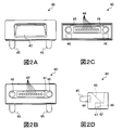
- FIG. 2 is a diagram illustrating a configuration of the optical coupling element 40 described in Patent Document 1.
- FIG. 2A is a plan view of the optical coupling element 40
- FIG. 2B is a bottom view
- FIG. 2C is a front view
- FIG. 2D is a right side view.
- the optical module 10 described in Patent Document 1 includes a substrate 20, a photoelectric conversion element 30 disposed on the substrate 20, and an optical coupling element 40 disposed on the substrate 20.
- the substrate 20 includes a substrate body 21 and first positioning protrusions 22 disposed on the substrate body 21. As shown in FIG.
- the optical coupling element 40 includes a concave portion 41 disposed on a surface facing the substrate 20, a first lens surface 42 (incident surface) for allowing light from the photoelectric conversion element 30 to enter, A total reflection surface 43 (reflection surface) that reflects light incident on one lens surface 42; a second lens surface 44 (output surface) that emits light reflected by the total reflection surface 43 toward the end surface of the optical fiber 50; A second positioning convex portion 45 for positioning the optical fiber 50 with respect to the optical coupling element 40; and a second positioning concave portion 46 for positioning the photoelectric conversion element 30 with respect to the optical coupling element 40 on the substrate 20;
- the optical coupling element 40 is placed on the first positioning convex portion 22 of the substrate 20 on which the photoelectric conversion element 30 is arranged.
- the second positioning recess 46 is mated.
- the first positioning concave portion 52 of the ferrule 51 that supports the optical fiber 50 is engaged with the second positioning convex portion 45 of the optical coupling element 40.
- the optical module 10 described in Patent Literature 1 optically connects the photoelectric conversion element 30 and the optical fiber 50 in this manner.
- thermosetting adhesive As a method of securely fixing the optical coupling element 40 described in Patent Document 1 to the substrate 20, it is conceivable to use a thermosetting adhesive.
- the optical coupling element 40 is fixed to the substrate 20 by applying an adhesive to the boundary between the side surface of the optical module 10 and the substrate 20 and curing the adhesive.
- thermosetting process with the recessed part 41 of the optical coupling element 40 sealed with the board
- the optical coupling element 40 fixed at an inappropriate position cannot appropriately couple the photoelectric conversion element 30 and the end face of the optical fiber 50.
- An optical receptacle according to the present invention is disposed between one or more photoelectric conversion elements arranged on a substrate and one or more optical transmission bodies, and the photoelectric conversion elements and the optical transmission bodies
- An optical receptacle for optically coupling an end surface to a concave portion formed on a contact surface that contacts the substrate and an inner surface of the concave portion to receive light emitted from the photoelectric conversion element Or one or two or more first optical surfaces that are emitted from the end face of the optical transmission body and pass through the interior toward the photoelectric conversion element, and are incident on the first optical surface and pass through the interior.
- One or two or more second optical surfaces that emit light toward the end face of the optical transmission body, or incident light emitted from the end face of the optical transmission body, the first optical surface, and the second optical Arranged on the light path between the surfaces, the first light Reflecting light incident on the surface toward the second optical surface or reflecting light incident on the second optical surface toward the first optical surface, and inside and outside of the recess And a communication portion that communicates with each other.
- the optical module according to the present invention is fixed on the substrate such that the substrate, one or more photoelectric conversion elements arranged on the substrate, and the first optical surface faces the photoelectric conversion element.
- the optical receptacle of the present invention is fixed to the surface of the substrate by an adhesive applied to a boundary between the side surface adjacent to the contact surface and the substrate.
- the present invention it is possible to provide an optical receptacle that is less likely to be misaligned even if it is fixed to a substrate using an adhesive. Even if the optical receptacle according to the present invention is fixed to a substrate using an adhesive, the photoelectric conversion element and the optical transmission body can be optically and appropriately combined.
- FIG. 1 is a diagram illustrating a configuration of an optical module according to Patent Document 1.
- FIG. 2A to 2D are diagrams showing the configuration of the optical coupling element according to Patent Document 1.
- FIG. 3 is a diagram illustrating a configuration of the optical module according to the first embodiment.
- 4A and 4B are perspective views of the optical receptacle according to Embodiment 1.
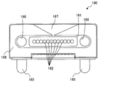
- FIG. 5A to 5D are diagrams showing the configuration of the optical receptacle according to the first embodiment.
- FIG. 6 is a bottom view of an optical receptacle according to a modification of the first embodiment.
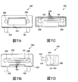
- 7A to 7D are diagrams showing the configuration of the optical receptacle according to the second embodiment.
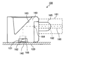
- FIG. 3 is a cross-sectional view of the optical module 100 according to Embodiment 1 of the present invention.
- hatching of the cross section of the optical receptacle 160 is omitted to show the optical path in the optical receptacle 160.
- the optical module 100 includes a substrate 120, one or more photoelectric conversion elements 140, and an optical receptacle 160.
- the optical module 100 is used with the optical transmission body 180 connected to the optical receptacle 160.
- the substrate 120 is provided with one or more photoelectric conversion elements 140 and an optical receptacle 160.
- a substrate-side convex portion 121 corresponding to a positioning concave portion 166 of an optical receptacle 160 described later is formed on the substrate 120.
- the optical receptacle 160 can be positioned at a predetermined position with respect to the photoelectric conversion element 140 disposed on the substrate 120.
- the material of the substrate 120 is not particularly limited.
- the substrate 120 is, for example, a glass composite substrate or a glass epoxy substrate.
- the photoelectric conversion element 140 is a light emitting element or a light receiving element, and is disposed on the substrate 120.
- a plurality (12) of photoelectric conversion elements 140 are arranged on the substrate 120.
- a light emitting element is used as the photoelectric conversion element 140.
- a light receiving element is used as the photoelectric conversion element 140.
- the light emitting element is, for example, a vertical cavity surface emitting laser (VCSEL).
- the light receiving element is, for example, a photo detector.
- the optical receptacle 160 is disposed on the substrate 120 so as to face the photoelectric conversion element 140.
- the optical receptacle 160 optically couples the photoelectric conversion element 140 and the end face of the optical transmission body 180 while being arranged between the photoelectric conversion element 140 and the optical transmission body 180.
- the optical receptacle 160 emits the light emitted from the photoelectric conversion element 140 (light emitting element) toward the end face of the optical transmission body 180.
- the optical receptacle 160 emits light emitted from the end face of the optical transmission body 180 toward the photoelectric conversion element 140 (light receiving element).
- the optical module 100 having both the light emitting element and the light receiving element as the photoelectric conversion element 140 functions as both a transmission optical module and a reception optical module.
- the configuration of the optical receptacle 160 will be described in detail separately.
- the type of the optical transmission body 180 is not particularly limited. Examples of types of the optical transmission body 180 include an optical fiber and an optical waveguide.
- the optical transmission body 180 is connected to the optical receptacle 160 via the ferrule 181.
- the ferrule 181 is formed with a ferrule-side recess 182 corresponding to a positioning protrusion 165 of an optical receptacle 160 described later.
- the end face of the optical transmission body 180 can be fixed at a predetermined position with respect to the optical receptacle 160.
- the optical transmission body 180 is an optical fiber.
- the optical fiber may be a single mode method or a multi mode method.
- FIG. 4A is a perspective view seen from the upper side (top surface side) of the optical receptacle 160 according to the present embodiment
- FIG. 4B is a perspective view seen from the lower side (bottom surface side).
- 5A is a plan view of the optical receptacle 160
- FIG. 5B is a bottom view
- FIG. 5C is a front view
- FIG. 5D is a side view.
- the optical receptacle 160 is a substantially rectangular parallelepiped member.
- the optical receptacle 160 includes a housing portion 161, a first optical surface 162, a third optical surface (reflection surface) 163, a second optical surface 164, a positioning convex portion 165, a positioning concave portion 166, and a communication portion 167.
- the optical receptacle 160 is formed using a material that is transparent to light having a wavelength used for optical communication. Examples of the material of the optical receptacle 160 include transparent resins such as polyetherimide (PEI) and cyclic olefin resin.
- PEI polyetherimide
- cyclic olefin resin examples of the optical receptacle 160 can be manufactured by injection molding, for example.
- the accommodating part 161 is a space (concave part) for accommodating the photoelectric conversion element 140.
- the accommodating portion 161 is disposed on the bottom surface that is the contact surface 168 with the substrate 120.
- the position of the accommodating portion 161 on the contact surface 168 is not particularly limited.
- the accommodating portion 161 may be disposed at the central portion of the contact surface 168 or may be disposed at a corner portion of the contact surface 168.
- the accommodating portion 161 is disposed at the central portion of the contact surface 168.
- the contact surface 168 is line symmetric.
- the bottom surface of the accommodating portion 161 is parallel to the surface of the substrate 120.
- “center” means that the margins (contact surfaces 168) are equal in the front-rear direction and the left-right direction of the optical receptacle 160.
- the first optical surface 162 allows light emitted from the photoelectric conversion element 140 (light emitting element) to enter the inside of the optical receptacle 160, or is incident on the second optical surface 164 and reflected on the third optical surface 163. Is an optical surface that emits light toward the photoelectric conversion element 140 (light receiving element).
- the first optical surface 162 is disposed on the bottom surface of the housing portion 161 (concave portion) so as to face the photoelectric conversion element 140.
- the two or more first optical surfaces 162 are arranged in a row in the long side direction on the bottom surface of the accommodating portion 161 so as to face the photoelectric conversion element 140. In the present embodiment, twelve first optical surfaces 162 are arranged in a line.
- the shape of the first optical surface 162 is not particularly limited.
- the shape of the first optical surface 162 is a convex lens surface that is convex toward the photoelectric conversion element 140. Further, the planar view shape of the first optical surface 162 is a circle.
- the central axis of the first optical surface 162 is preferably perpendicular to the light emitting surface or the light receiving surface of the photoelectric conversion element 140 (and the surface of the substrate 120).
- the central axis of the first optical surface 162 preferably coincides with the optical axis of light emitted from the photoelectric conversion element 140 (light emitting element) or light incident on the photoelectric conversion element 140 (light receiving element).
- the first optical surface 162 is not limited to two or more, and may be one.
- the third optical surface 163 reflects the light incident on the first optical surface 162 toward the second optical surface 164 or reflects the light incident on the second optical surface 164 toward the first optical surface 162. It is a surface (reflection surface).
- the third optical surface 163 is inclined so as to approach the optical transmission body 180 (front side) from the bottom surface of the optical receptacle 160 toward the top surface.
- the inclination angle of the third optical surface 163 is not particularly limited. In the present embodiment, the inclination angle of the third optical surface 163 is 45 ° with respect to the optical axis of the light incident on the third optical surface 163.
- the shape of the third optical surface 163 is not particularly limited. In the present embodiment, the shape of the third optical surface 163 is a plane. The light incident on the first optical surface 162 or the second optical surface 164 is incident on the third optical surface 163 at an incident angle larger than the critical angle.
- the second optical surface 164 emits the light incident on the first optical surface 162 and reflected by the third optical surface 163 toward the end surface of the light transmission body 180 or emitted from the end surface of the light transmission body 180.
- Two or more second optical surfaces 164 are arranged in a row in the long side direction on the front surface of the optical receptacle 160 so as to face the end surface of the optical transmission body 180, respectively.
- twelve second optical surfaces 164 are arranged in a line.
- the shape of the second optical surface 164 is not particularly limited.
- the shape of the second optical surface 164 is a convex lens surface that is convex toward the end surface of the optical transmission body 180.
- the central axis of the second optical surface 164 is preferably coincident with the central axis of the end face of the optical transmission body 180.
- the second optical surface 164 is not limited to two or more, and may be one.
- the positioning convex portion 165 fixes the end surface of the optical transmission body 180 at a desired position with respect to the second optical surface 164.
- the positioning convex portion 165 is fitted into the ferrule-side concave portion 182 formed in the ferrule 181 of the optical transmission body 180 as described above.
- the shape and size of the positioning convex portion 165 are not particularly limited as long as the above-described effects can be exhibited.
- the positioning recess 166 fixes the first optical surface 162 at a desired position with respect to the photoelectric conversion element 140. As described above, the substrate-side convex portion 121 formed on the substrate 120 is fitted into the positioning concave portion 166.
- the shape and size of the positioning recess 166 are not particularly limited as long as the above-described effects can be exhibited.
- the positioning recess 166 is a substantially cylindrical recess.
- the communication unit 167 communicates the inside and the outside of the housing unit 161.
- the shape of the communication portion 167 is not particularly limited as long as the above-described function can be exhibited.
- Examples of the shape of the communication portion 167 include a communication groove or a communication hole that is open to the inner surface of the housing portion 161 and the outer surface adjacent to the contact surface 168.
- the communication portion 167 is a communication groove that is disposed on the contact surface 168 and opens on the inner surface of the housing portion 161 and the outer surface adjacent to the contact surface 168.
- the position of the communication groove on the contact surface 168 is not particularly limited.
- the communication groove is disposed so as to connect the central portion in the long side direction of the accommodating portion 161 and the central portion in the long side direction at the bottom of the back surface adjacent to the contact surface 168. That is, the communication groove extends in a straight line and is arranged so that its central axis passes through the center of the accommodating portion 161.
- the cross-sectional shape of the communication groove is not particularly limited.
- the cross-sectional shape of the communication groove may be a triangle or a rectangle. In the present embodiment, the cross-sectional shape of the communication groove is a rectangle. Further, the cross-sectional area of the communication groove is not particularly limited.
- the cross-sectional area of the communication groove is preferably a size that does not serve as a liquid passage, although it serves as a gas passage.
- the width of the communication groove may be the same on the accommodating portion 161 side and the outer surface side adjacent to the contact surface 168, or may be different. In the present embodiment, the width of the communication groove is constant.
- the optical path in the optical module 100 will be described.
- the optical receptacle 160 When the optical receptacle 160 is used in the optical module 100 for transmission, light emitted from the photoelectric conversion element 140 (light emitting element) enters the optical receptacle 160 through the first optical surface 162. At this time, the light incident on the optical receptacle 160 is converted into collimated light by the first optical surface 162 and travels toward the third optical surface 163. Next, the light incident on the optical receptacle 160 is reflected by the third optical surface 163 and emitted toward the second optical surface 164. The light reflected by the third optical surface 163 and emitted outside the optical receptacle 160 by the second optical surface 164 reaches the end surface of the optical transmission body 180 while converging.
- the optical receptacle 160 When the optical receptacle 160 is used for the optical module 100 for reception, the light emitted from the end face of the optical transmission body 180 enters the optical receptacle 160 through the second optical surface 164. At this time, the light incident on the optical receptacle 160 is converted into collimated light by the third optical surface 163 and travels toward the third optical surface 163. Next, the light incident on the optical receptacle 160 is reflected by the third optical surface 163 and emitted toward the first optical surface 162. The light reflected by the third optical surface 163 and emitted to the outside of the optical receptacle 160 by the first optical surface 162 reaches the photoelectric conversion element 140 (light receiving element) while converging.
- the photoelectric conversion element 140 light receiving element
- the method for assembling optical module 100 according to the present embodiment is not particularly limited.
- the optical module 100 can be assembled by fixing the optical receptacle 160 using a thermosetting adhesive.
- the photoelectric conversion element 140 is fixed at a predetermined position of the substrate 120. Specifically, each photoelectric conversion element 140 is arranged so as to face each first optical surface 162 of the optical receptacle 160.
- the optical receptacle 160 is placed on the substrate 120 on which the photoelectric conversion element 140 is disposed. Specifically, the positioning concave portion 166 of the optical receptacle 160 is engaged with the substrate-side convex portion 121 of the substrate 120. Thereby, the optical receptacle 160 can be arranged so that the central axis of the photoelectric conversion element 140 and the central axis of the first optical surface 162 coincide with each other.
- thermosetting resin is formed at the boundary between the surface of the substrate 120 and the outer surface (front surface, back surface, right side surface, and left side surface) adjacent to the contact surface 168 (bottom surface) excluding the location where the communication groove is opened.
- the thermosetting temperature is about 100 ° C.
- the thermosetting time is 30 minutes. Degree.
- the adhesive immediately after being applied enters slightly between the surface of the substrate 120 and the contact surface 168, but hardly enters the inside of the accommodating portion 161 from the opening of the communication groove. Further, during the thermosetting process, the air in the accommodating portion 161 expands and is discharged to the outside via the communication groove, so that the adhesive does not enter the accommodating portion 161 via the communication groove. Note that the amount of adhesive that has entered the contact surface with the surface of the substrate 120 is extremely small, so that the performance of the optical module 100 is not affected.
- the optical module 100 according to the present embodiment can be assembled through the above steps.
- the optical receptacle 160 has a communication portion 167 that communicates the inside and the outside of the housing portion 161 formed on the contact surface (bottom surface) 168 with the surface of the substrate 120. For this reason, the air in the accommodating part 161 is discharged
- FIG. 6 is a bottom view of an optical receptacle 160 according to a modification of the first embodiment.
- the width of the communication groove may be formed so that the accommodating portion 161 side is narrow and widens toward the outer surface adjacent to the contact surface 168. In this case, the opening of the communication groove is not blocked by the adhesive. Even when the adhesive reaches the opening end of the communication groove, the distance to the first optical surface 162 is long, so that the adhesive reaches the first optical surface 162 and affects the optical characteristics. There is nothing.
- the optical module according to the second embodiment is different from the optical module 100 according to the first embodiment only in the configuration of the optical receptacle 260. Therefore, the same components as those of the optical module 100 according to Embodiment 1 are denoted by the same reference numerals, and the description thereof is omitted.
- FIG. 7 is a diagram showing a configuration of the optical receptacle 260 according to the second embodiment.
- 7A is a plan view of the optical receptacle 260
- FIG. 7B is a bottom view
- FIG. 7C is a front view
- FIG. 7D is a side view.
- the optical module according to Embodiment 2 includes a substrate 120, a photoelectric conversion element 140, and an optical receptacle 260.
- the optical receptacle 260 includes a housing portion 161, a first optical surface 162, a third optical surface 163 (reflection surface), a second optical surface 164, a positioning convex portion 165, a positioning concave portion 266 and a communication portion 267.
- the positioning recess 266 is a through hole that opens to the contact surface 168 (bottom surface) and the top surface of the optical receptacle 260, respectively.
- the communication portion 267 is a communication groove that communicates the inside and the outside of the housing portion 161.
- the communication groove is disposed so as to connect the central portion in the short side direction of the accommodating portion 161 and the inner surface of the positioning recess 266 (the outer surface adjacent to the contact surface 168).
- one communication groove may be disposed at one end portion in the long side direction of the accommodating portion 161, or two communication grooves may be disposed at both ends in the long side direction of the accommodating portion 161.
- one is disposed at one end of the accommodating portion 161 in the long side direction.
- the positioning recess 266 of the optical receptacle 260 is engaged with the substrate-side convex portion 121 of the substrate 120.
- an adhesive made of a thermosetting resin is applied to the boundary between the surface of the substrate 120 and the outer surface adjacent to the contact surface 168 (front surface, back surface, right side surface, and left side surface). Heat cure treatment in time.
- the adhesive immediately after application does not enter the inside of the accommodating portion 161.
- the air expanded in the accommodating part 161 is discharged
- the optical module according to the second embodiment has the same effect as the optical module 100 according to the first embodiment.
- the first optical surface 162 and the second optical surface 164 are convex lens surfaces.
- the first optical surface 162 and the second optical surface 164 are flat surfaces. It may be. Specifically, only the first optical surface 162 may be a flat surface, or only the second optical surface 164 may be a flat surface.
- the third optical surface 163 is formed so as to function as a concave mirror.
- the second optical surface 164 is formed in a plane. Also good.
- the reference position of the first optical surface 162 is not particularly limited.
- the optical module 100 includes a light emitting element and a light receiving element as a plurality of photoelectric conversion elements.
- optical receptacle and the optical module according to the present invention are useful for optical communication using an optical transmission body.
Landscapes
- Physics & Mathematics (AREA)
- General Physics & Mathematics (AREA)
- Optics & Photonics (AREA)
- Optical Couplings Of Light Guides (AREA)
Abstract
本発明の光レセプタクルは、基板に当接する当接面に形成された凹部と、凹部の底に配置され、光電変換素子から出射された光を入射させるか、光伝送体の端面から出射され、内部を通る光を光電変換素子に向けて出射させる第1光学面と、第1光学面で入射し、内部を通る光を光伝送体の端面に向けて出射させるか、光伝送体の端面から出射された光を入射させる第2光学面と、第1光学面および第2光学面の間の光の光路上に配置され、第1光学面で入射した光を第2光学面に向かって反射させるか、第2光学面で入射した光を第1光学面に向かって反射させるための反射面と、凹部の内部と外部を連通する連通部と、を有する。
Description
本発明は、光レセプタクルおよびこれを有する光モジュールに関する。
以前から、光ファイバーや光導波路などの光伝送体を用いた光通信には、面発光レーザ(例えば、垂直共振器面発光レーザ(VCSEL:Vertical Cavity Surface Emitting Laser))などの発光素子を備えた光モジュールが使用されている。光モジュールは、1または2以上の光電変換素子(発光素子および受光素子)と、送信用または受信用の光結合素子(以下、「光レセプタクル」ともいう)とを有する(例えば、特許文献1参照)。
図1は、特許文献1に記載の光モジュール10の構成を示す図である。図2は、特許文献1に記載の光結合素子40の構成を示す図である。図2Aは、光結合素子40の平面図であり、図2Bは、底面図であり、図2Cは、正面図であり、図2Dは、右側面図である。
図1に示されるように、特許文献1に記載の光モジュール10は、基板20と、基板20上に配置された光電変換素子30と、基板20上に配置された光結合素子40とを有する。基板20は、基板本体21と、基板本体21の上に配置された第1位置決め用凸部22とを有する。図2に示されるように、光結合素子40は、基板20に対向した面に配置された凹部41と、光電変換素子30からの光を入射させる第1レンズ面42(入射面)と、第1レンズ面42で入射した光を反射させる全反射面43(反射面)と、全反射面43で反射された光を光ファイバー50の端面に向けて出射させる第2レンズ面44(出射面)と、光ファイバー50を光結合素子40に対して位置決めするための第2位置決め用凸部45と、光電変換素子30を光結合素子40に対して基板20に位置決めするための第2位置決め用凹部46とを有する。
図1に示されるように、特許文献1に記載の光モジュール10を組み立てる場合、まず、光電変換素子30が配置された基板20の第1位置決め用凸部22に対して、光結合素子40の第2位置決め用凹部46を篏合させる。次に、光結合素子40の第2位置決め用凸部45に光ファイバー50を支持しているフェルール51の第1位置決め用凹部52を篏合させる。特許文献1に記載の光モジュール10は、このようにして光電変換素子30と光ファイバー50とを光学的に接続している。
特許文献1に記載の光結合素子40を基板20に確実に固定する方法として、熱硬化性の接着剤を使用することが考えられる。たとえば、光モジュール10の側面と基板20との境界に接着剤を塗布して熱硬化させることで、基板20に対して光結合素子40を固定する。
このように特許文献1に記載の光結合素子40を熱硬化性の接着剤を用いて固定する場合、光結合素子40の凹部41が基板20および接着剤により密閉された状態で熱硬化処理(加熱)を行うため、凹部41内の空気が膨張して、光結合素子40の位置をずらしてしまうおそれがある。このように不適切な位置に固定された光結合素子40は、光電変換素子30と光ファイバー50の端面とを適切に結合させることができない。
そこで、本発明の目的は、基板に対して接着剤を用いて固定しても、位置ズレが生じにくい光レセプタクルを提供することである。また、本発明の別の目的は、この光レセプタクルを有する光モジュールを提供することでもある。
本発明に係る光レセプタクルは、基板上に配置される1または2以上の光電変換素子と、1または2以上の光伝送体との間に配置され、前記光電変換素子と、前記光伝送体の端面とを光学的に結合するための光レセプタクルであって、前記基板と当接する当接面に形成された凹部と、前記凹部の内面に配置され、前記光電変換素子から出射された光を入射させるか、前記光伝送体の端面から出射され、内部を通る光を前記光電変換素子に向けて出射させる1または2以上の第1光学面と、前記第1光学面で入射し、内部を通る光を前記光伝送体の端面に向けて出射させるか、前記光伝送体の端面から出射された光を入射させる1または2以上の第2光学面と、前記第1光学面および前記第2光学面の間の光の光路上に配置され、前記第1光学面で入射した光を前記第2光学面に向かって反射させるか、前記第2光学面で入射した光を前記第1光学面に向かって反射させるための反射面と、前記凹部の内部と外部を連通する連通部と、を有する。
本発明に係る光モジュールは、基板と、前記基板上に配置された1または2以上の光電変換素子と、前記第1光学面が前記光電変換素子と対向するように前記基板上に固定された本発明の光レセプタクルと、を有し、前記光レセプタクルは、前記当接面に隣接する側面と前記基板との境界に塗布された接着剤により、前記基板の表面に固定されている。
本発明によれば、基板に対して接着剤をもちいて固定しても、位置ズレが生じにくい光レセプタクルを提供することができる。本発明に係る光レセプタクルは、接着剤を用いて基板に固定されても、光電変換素子と光伝送体とを光学的に適切に結合させることができる。
以下、本発明の実施の形態に係る光レセプタクルおよび光モジュールについて、図面を参照して詳細に説明する。
[実施の形態1]
(光モジュールの構成)
図3は、本発明の実施の形態1に係る光モジュール100の断面図である。図3では、光レセプタクル160内の光路を示すために光レセプタクル160の断面へのハッチングを省略している。
(光モジュールの構成)
図3は、本発明の実施の形態1に係る光モジュール100の断面図である。図3では、光レセプタクル160内の光路を示すために光レセプタクル160の断面へのハッチングを省略している。
図3に示されるように、光モジュール100は、基板120と、1または2以上の光電変換素子140と、光レセプタクル160とを有する。光モジュール100は、光レセプタクル160に光伝送体180が接続されて使用される。
基板120には、1または2以上の光電変換素子140および光レセプタクル160が配置される。基板120には、後述する光レセプタクル160の位置決め用凹部166に対応した基板側凸部121が形成されている。この基板側凸部121に位置決め用凹部166を嵌め込むことにより、光レセプタクル160を、基板120上に配置された光電変換素子140に対して所定の位置に位置決めすることができる。基板120の材料は、特に限定されない。基板120は、例えばガラスコンポジット基板やガラスエポキシ基板などである。
光電変換素子140は、発光素子または受光素子であり、基板120上に配置されている。本実施の形態では、複数(12個)の光電変換素子140(発光素子および/または受光素子)が、基板120上に配置されている。送信用の光モジュール100では、光電変換素子140として発光素子が使用される。受信用の光モジュール100では、光電変換素子140として受光素子が使用される。発光素子は、例えば垂直共振器面発光レーザ(VCSEL)である。受光素子は、例えばフォトディテクタである。
光レセプタクル160は、光電変換素子140と対向するように基板120上に配置されている。光レセプタクル160は、光電変換素子140と光伝送体180との間に配置された状態で、光電変換素子140と光伝送体180の端面とを光学的に結合させる。送信用の光モジュール100では、光レセプタクル160は、光電変換素子140(発光素子)から出射された光を光伝送体180の端面に向けて出射する。受信用の光モジュール100では、光レセプタクル160は、光伝送体180の端面から出射された光を光電変換素子140(受光素子)に向けて出射する。なお、光電変換素子140として発光素子および受光素子の両方を有する光モジュール100は、送信用の光モジュールおよび受信用の光モジュールの両方として機能する。光レセプタクル160の構成については、別途詳細に説明する。
光伝送体180の種類は、特に限定されない。光伝送体180の種類の例には、光ファイバーや光導波路などが含まれる。光伝送体180は、フェルール181を介して光レセプタクル160に接続される。フェルール181には、後述する光レセプタクル160の位置決め用凸部165に対応したフェルール側凹部182が形成されている。このフェルール側凹部182を位置決め用凸部165に嵌め込むことにより、光伝送体180の端面を光レセプタクル160に対して所定の位置に固定することができる。本実施の形態では、光伝送体180は、光ファイバーである。また、光ファイバーは、シングルモード方式であってもよいし、マルチモード方式であってもよい。
(光レセプタクルの構成)
図4および図5は、実施の形態に係る光レセプタクル160の構成を示す図である。図4Aは、本実施の形態に係る光レセプタクル160の上側(天面側)からみた斜視図であり、図4Bは、下側(底面側)からみた斜視図である。図5Aは、光レセプタクル160の平面図であり、図5Bは、底面図であり、図5Cは、正面図であり、図5Dは、側面図である。
図4および図5は、実施の形態に係る光レセプタクル160の構成を示す図である。図4Aは、本実施の形態に係る光レセプタクル160の上側(天面側)からみた斜視図であり、図4Bは、下側(底面側)からみた斜視図である。図5Aは、光レセプタクル160の平面図であり、図5Bは、底面図であり、図5Cは、正面図であり、図5Dは、側面図である。
図4および図5に示されるように、光レセプタクル160は、略直方体形状の部材である。光レセプタクル160は、収容部161、第1光学面162、第3光学面(反射面)163、第2光学面164、位置決め用凸部165、位置決め用凹部166および連通部167を有する。光レセプタクル160は、光通信に用いられる波長の光に対して透光性を有する材料を用いて形成される。光レセプタクル160の材料の例には、ポリエーテルイミド(PEI)や環状オレフィン樹脂などの透明な樹脂が含まれる。また、光レセプタクル160は、例えば射出成形により製造されうる。
収容部161は、光電変換素子140を収容するための空間(凹部)である。収容部161は、基板120との当接面168である底面に配置されている。当接面168における収容部161の位置は、特に限定されない。たとえば、収容部161は、当接面168の中央部分に配置されていてもよいし、当接面168の隅部分に配置されていてもよい。本実施の形態では、収容部161は、当接面168の中央部分に配置されている。この場合、当接面168は、線対称となる。収容部161の底面は、基板120の表面と平行である。ここで、「中央」とは、光レセプタクル160の前後方向および左右方向において、余白(当接面168)がそれぞれ等しい場合を意味する。
第1光学面162は、光電変換素子140(発光素子)から出射された光を光レセプタクル160の内部に入射させるか、第2光学面164で入射し、第3光学面163で反射された光を光電変換素子140(受光素子)に向けて出射させる光学面である。第1光学面162は、光電変換素子140に対向できるように収容部161(凹部)の底面に配置されている。2個以上の第1光学面162は、収容部161の底面に、光電変換素子140と対向するように長辺方向に一列に配置される。本実施の形態では、12個の第1光学面162が一列に配置されている。第1光学面162の形状は、特に限定されない。本実施の形態では、第1光学面162の形状は、光電変換素子140に向かって凸状の凸レンズ面である。また、第1光学面162の平面視形状は、円形である。第1光学面162の中心軸は、光電変換素子140の発光面または受光面(および基板120の表面)に対して垂直であることが好ましい。また、第1光学面162の中心軸は、光電変換素子140(発光素子)から出射された光、または光電変換素子140(受光素子)に入射する光の光軸と一致することが好ましい。なお、第1光学面162は、2個以上に限定されず、1個であってもよい。
第3光学面163は、第1光学面162で入射した光を第2光学面164に向けて反射させるか、第2光学面164で入射した光を第1光学面162に向けて反射させる光学面(反射面)である。第3光学面163は、光レセプタクル160の底面から天面に向かうにつれて、光伝送体180(正面側)に近づくように傾斜している。第3光学面163の傾斜角度は、特に限定されない。本実施の形態では、第3光学面163の傾斜角度は、第3光学面163に入射する光の光軸に対して45°である。第3光学面163の形状は、特に限定されない。本実施の形態では、第3光学面163の形状は、平面である。第3光学面163には、第1光学面162または第2光学面164で入射した光が、臨界角より大きな入射角で入射する。
第2光学面164は、第1光学面162で入射し、第3光学面163で反射された光を光伝送体180の端面に向けて出射させるか、光伝送体180の端面から出射された光を光レセプタクル160の内部に入射させる光学面である。2個以上の第2光学面164は、光レセプタクル160の正面に、光伝送体180の端面とそれぞれ対向するように長辺方向に一列に配置されている。本実施の形態では、12個の第2光学面164が一列に配置されている。第2光学面164の形状は、特に限定されない。本実施の形態では、第2光学面164の形状は、光伝送体180の端面に向かって凸状の凸レンズ面である。第2光学面164の中心軸は、光伝送体180の端面の中心軸と一致していることが好ましい。なお、第2光学面164は、2個以上に限定されず、1個であってもよい。
位置決め用凸部165は、光伝送体180の端面を第2光学面164に対して所望の位置に固定する。位置決め用凸部165は、前述のとおり光伝送体180のフェルール181に形成されたフェルール側凹部182に嵌め込まれる。位置決め用凸部165の形状および大きさは、前述の効果を発揮することができれば、特に限定されない。
位置決め用凹部166は、第1光学面162を光電変換素子140に対して所望の位置に固定する。位置決め用凹部166には、前述の通り基板120に形成された基板側凸部121が嵌め込まれる。位置決め用凹部166の形状および大きさは、前述の効果を発揮することができれば、特に限定されない。本実施の形態では、位置決め用凹部166は、略円柱形状の凹部である。
連通部167は、収容部161の内部と外部を連通する。連通部167の形状は、前述の機能を発揮することができれば、特に限定されない。連通部167の形状の例には、収容部161の内面と当接面168に隣接する外表面とに開口した、連通溝または連通孔などがある。本実施の形態では、連通部167は、当接面168に配置され、収容部161の内面と当接面168に隣接する外表面に開口した連通溝である。当接面168における連通溝の位置は、特に限定されない。本実施の形態では、連通溝は、収容部161の長辺方向の中央部分と、当接面168に隣接する背面最下部の長辺方向の中央部分とを繋ぐように配置されている。すなわち、連通溝は、直線状に延在しており、その中心軸が収容部161の中心を通るように配置されている。連通溝の断面形状は、特に限定されない。連通溝の断面形状は、三角形であってもよいし、矩形であってもよい。本実施の形態では、連通溝の断面形状は、矩形である。また、連通溝の断面積も特に限定されない。連通溝の断面積は、気体の通り道とはなるが、液体の通り道とはならない程度の大きさであることが好ましい。連通溝の幅は、収容部161側と当接面168に隣接する外表面側とで同じであってもよいし、異なっていてもよい。本実施の形態では、連通溝の幅は、一定である。
次いで、本実施の形態に係る光モジュール100における光路について説明する。光レセプタクル160を送信用の光モジュール100で使用する場合、光電変換素子140(発光素子)から出射された光は、第1光学面162で光レセプタクル160の内部に入射する。このとき、光レセプタクル160に入射した光は、第1光学面162によってコリメート光に変換され、第3光学面163に向かって進行する。次いで、光レセプタクル160に入射した光は、第3光学面163で反射され、第2光学面164に向かって出射される。第3光学面163で反射され、第2光学面164で光レセプタクル160の外部に出射された光は、収束しながら光伝送体180の端面に到達する。
光レセプタクル160を受信用の光モジュール100に使用する場合、光伝送体180の端面から出射された光は、第2光学面164で光レセプタクル160の内部に入射する。このとき、光レセプタクル160に入射した光は、第3光学面163によってコリメート光に変換され、第3光学面163に向かって進行する。次いで、光レセプタクル160に入射した光は、第3光学面163で反射され、第1光学面162に向かって出射される。第3光学面163で反射され、第1光学面162で光レセプタクル160の外部に出射された光は、収束しながら光電変換素子140(受光素子)に到達する。
(光モジュールの組み立て方法)
本実施の形態に係る光モジュール100の組み立て方法は、特に限定されない。たとえば、基板120上に光電変換素子140を固定した後に、光レセプタクル160を熱硬化性の接着剤を用いて固定することで、光モジュール100を組み立てることができる。
本実施の形態に係る光モジュール100の組み立て方法は、特に限定されない。たとえば、基板120上に光電変換素子140を固定した後に、光レセプタクル160を熱硬化性の接着剤を用いて固定することで、光モジュール100を組み立てることができる。
まず、基板120の所定の位置に、光電変換素子140を固定する。具体的には、光レセプタクル160の各第1光学面162に対向できるように各光電変換素子140を配置する。次いで、光電変換素子140が配置された基板120上に、光レセプタクル160を載置する。具体的には、基板120の基板側凸部121に光レセプタクル160の位置決め用凹部166を篏合させる。これにより、光電変換素子140の中心軸と、第1光学面162との中心軸とが一致するように光レセプタクル160を配置することができる。
次いで、連通溝が開口している箇所を除く、基板120の表面と当接面168(底面)に隣接する外表面(正面、背面、右側面および左側面)との境界部分に熱硬化性樹脂からなる接着剤を塗布する。その後、所定の温度および所定の時間で熱硬化処理する。なお、本実施形態では、熱硬硬化性の接着剤としてAblestik BF-4(ヘンケルジャパン株式会社)を使用した場合、熱硬化処理温度は、100℃程度であり、熱硬化処理時間は、30分程度である。
このとき、塗布した直後の接着剤は、基板120の表面と当接面168との間に僅かながら入り込むが、連通溝の開口部から収容部161の内部に入り込むことはほとんどない。また、熱硬化処理時においては、収容部161内の空気が膨張して連通溝を経由して外部に排出されるため、接着剤が連通溝を介して収容部161内に入り込むことはない。なお、基板120の表面と当接面に入り込んだ接着剤は、極めて微量であるため、光モジュール100の性能に影響を及ぼすことはない。
以上の工程により、本実施の形態に係る光モジュール100を組み立てることができる。
(効果)
本実施の形態に係る光レセプタクル160は、基板120の表面との当接面(底面)168に形成された収容部161の内部と外部を連通する連通部167を有する。このため、熱硬化処理時において、収容部161内の空気が連通部167を介して外部に排出される。また、基板120に対して光レセプタクル160が部分的に浮くことがないため、従来技術のように光レセプタクル160が位置ズレすることがない。よって、本実施の形態に係る光モジュール100では、基板120に対する光レセプタクル160の設置精度が高いため、光電変換素子140と光伝送体180とを光学的に適切に結合させることができる。
本実施の形態に係る光レセプタクル160は、基板120の表面との当接面(底面)168に形成された収容部161の内部と外部を連通する連通部167を有する。このため、熱硬化処理時において、収容部161内の空気が連通部167を介して外部に排出される。また、基板120に対して光レセプタクル160が部分的に浮くことがないため、従来技術のように光レセプタクル160が位置ズレすることがない。よって、本実施の形態に係る光モジュール100では、基板120に対する光レセプタクル160の設置精度が高いため、光電変換素子140と光伝送体180とを光学的に適切に結合させることができる。
前述のとおり、連通部167の形状は特に限定されない。図6は、実施の形態1の変形例に係る光レセプタクル160の底面図である。図6に示されるように、連通溝の幅は、収容部161側が狭く形成されていて、当接面168に隣接する外表面に向かうにつれて、広がるように形成されていてもよい。この場合、連通溝の開口が接着剤で塞がってしまうことがない。また、接着剤が連通溝の開口端部に到達した場合であっても、第1光学面162までの距離が長いため、接着剤が第1光学面162に到達して光学特性に影響を及ぼすことがない。
[実施の形態2]
(光モジュールの構成)
実施の形態2に係る光モジュールは、光レセプタクル260の構成のみが実施の形態1に係る光モジュール100と異なる。そこで、実施の形態1に係る光モジュール100と同一の構成については、同一の符号を付してその説明を省略する。
(光モジュールの構成)
実施の形態2に係る光モジュールは、光レセプタクル260の構成のみが実施の形態1に係る光モジュール100と異なる。そこで、実施の形態1に係る光モジュール100と同一の構成については、同一の符号を付してその説明を省略する。
図7は、実施の形態2に係る光レセプタクル260の構成を示す図である。図7Aは、光レセプタクル260の平面図であり、図7Bは、底面図であり、図7Cは、正面図であり、図7Dは、側面図である。
実施の形態2に係る光モジュールは、基板120、光電変換素子140および光レセプタクル260を有する。
(光レセプタクルの構成)
光レセプタクル260は、収容部161、第1光学面162、第3光学面163(反射面)、第2光学面164、位置決め用凸部165、位置決め用凹部266および連通部267を有する。
光レセプタクル260は、収容部161、第1光学面162、第3光学面163(反射面)、第2光学面164、位置決め用凸部165、位置決め用凹部266および連通部267を有する。
位置決め用凹部266は、光レセプタクル260の当接面168(底面)および天面にそれぞれ開口した貫通孔である。
連通部267は、収容部161の内部と外部を連通する連通溝である。本実施の形態では、連通溝は、収容部161の短辺方向の中央部分と、位置決め用凹部266の内面(当接面168に隣接する外表面)とを繋ぐように配置されている。この場合、連通溝は、収容部161の長辺方向の一方の端部に1個配置されていてもよいし、収容部161の長辺方向の両端に2個配置されていてもよい。本実施の形態では、収容部161の長辺方向の一方の端部に1個配置されている。
実施の形態2に係る光モジュールの組み立て方法では、基板120に対して光電変換素子140を配置した後に、基板120の基板側凸部121に光レセプタクル260の位置決め用凹部266を篏合させる。次いで、基板120の表面と当接面168に隣接する外表面(正面、背面、右側面および左側面)との境界に熱硬化性樹脂からなる接着剤を塗布した後、所定の温度および所定の時間で熱硬化処理する。このとき、塗布した直後の接着剤が、収容部161の内部に入り込むことはない。また、収容部161内で膨張した空気は、連通溝を経由して貫通孔から外部に排出される。
(効果)
実施の形態2に係る光モジュールは、実施の形態1に係る光モジュール100と同様の効果を有する。
実施の形態2に係る光モジュールは、実施の形態1に係る光モジュール100と同様の効果を有する。
なお、上記実施の形態に係る光レセプタクル160、260では、第1光学面162および第2光学面164が凸レンズ面である場合を示したが、第1光学面162および第2光学面164は平面であってもよい。具体的には、第1光学面162のみが平面であってもよいし、第2光学面164のみが平面であってもよい。第1光学面162が平面に形成されている場合、例えば、第3光学面163は、凹面鏡として機能できるように形成される。また、第1光学面162や第3光学面163などにより、第2光学面164に到達する直前の光が効果的に収束されている場合は、第2光学面164が平面に形成されていてもよい。なお、この場合、第1光学面162の基準位置は、特に限定されない。
また、上記の実施の形態では、光レセプタクル160、260を送信用または受信用の光モジュール100で使用する場合について説明したが、本発明に係る光モジュール100は、送受信用の光モジュールでも使用されうる。この場合、光モジュールは、複数の光電変換素子として発光素子および受光素子を含む。
本出願は、2014年7月31日出願の特願2014-156491に基づく優先権を主張する。当該出願明細書および図面に記載された内容は、すべて本願明細書に援用される。
本発明に係る光レセプタクルおよび光モジュールは、光伝送体を用いた光通信に有用である。
10 光モジュール
20 基板
21 基板本体
22 第1位置決め用凸部
30 光電変換素子
40 光結合素子
41 凹部
42 第1レンズ面
43 反射面
44 第2レンズ面
45 第2位置決め用凸部
46 第2位置決め用凹部
50 光ファイバー
51 フェルール
52 第1位置決め用凹部
100 光モジュール
120 基板
121 基板側凸部
140 光電変換素子
160、260 光レセプタクル
161 収容部(凹部)
162 第1光学面
163 第3光学面
164 第2光学面
165 位置決め用凸部
166、266 位置決め用凹部
167、267 連通部
168 当接面
180 光伝送体
181 フェルール
182 フェルール側凹部
20 基板
21 基板本体
22 第1位置決め用凸部
30 光電変換素子
40 光結合素子
41 凹部
42 第1レンズ面
43 反射面
44 第2レンズ面
45 第2位置決め用凸部
46 第2位置決め用凹部
50 光ファイバー
51 フェルール
52 第1位置決め用凹部
100 光モジュール
120 基板
121 基板側凸部
140 光電変換素子
160、260 光レセプタクル
161 収容部(凹部)
162 第1光学面
163 第3光学面
164 第2光学面
165 位置決め用凸部
166、266 位置決め用凹部
167、267 連通部
168 当接面
180 光伝送体
181 フェルール
182 フェルール側凹部
Claims (4)
- 基板上に配置される1または2以上の光電変換素子と、1または2以上の光伝送体との間に配置され、前記光電変換素子と、前記光伝送体の端面とを光学的に結合するための光レセプタクルであって、
前記基板と当接する当接面に形成された凹部と、
前記凹部の内面に配置され、前記光電変換素子から出射された光を入射させるか、前記光伝送体の端面から出射され、内部を通る光を前記光電変換素子に向けて出射させる1または2以上の第1光学面と、
前記第1光学面で入射し、内部を通る光を前記光伝送体の端面に向けて出射させるか、前記光伝送体の端面から出射された光を入射させる1または2以上の第2光学面と、
前記第1光学面および前記第2光学面の間の光の光路上に配置され、前記第1光学面で入射した光を前記第2光学面に向かって反射させるか、前記第2光学面で入射した光を前記第1光学面に向かって反射させるための反射面と、
前記凹部の内部と外部を連通する連通部と、
を有する、光レセプタクル。 - 前記連通部は、前記当接面に形成され、前記凹部の内面と前記当接面に隣接する外表面に開口した連通溝である、請求項1に記載の光レセプタクル。
- 前記当接面は、線対称である、請求項2に記載の光レセプタクル。
- 基板と、
前記基板上に配置された1または2以上の光電変換素子と、
前記第1光学面が前記光電変換素子と対向するように前記基板上に固定された請求項1~3のいずれか一項に記載の光レセプタクルと、を有し、
前記光レセプタクルは、前記当接面に隣接する側面と前記基板との境界に塗布された接着剤により、前記基板の表面に固定されている、
光モジュール。
Priority Applications (2)
| Application Number | Priority Date | Filing Date | Title |
|---|---|---|---|
| US15/500,394 US9939594B2 (en) | 2014-07-31 | 2015-07-16 | Optical receptacle and optical module |
| CN201580040065.1A CN106537205B (zh) | 2014-07-31 | 2015-07-16 | 光插座及光模块 |
Applications Claiming Priority (2)
| Application Number | Priority Date | Filing Date | Title |
|---|---|---|---|
| JP2014156491A JP6461506B2 (ja) | 2014-07-31 | 2014-07-31 | 光レセプタクルおよび光モジュール |
| JP2014-156491 | 2014-07-31 |
Publications (1)
| Publication Number | Publication Date |
|---|---|
| WO2016017433A1 true WO2016017433A1 (ja) | 2016-02-04 |
Family
ID=55217338
Family Applications (1)
| Application Number | Title | Priority Date | Filing Date |
|---|---|---|---|
| PCT/JP2015/070351 Ceased WO2016017433A1 (ja) | 2014-07-31 | 2015-07-16 | 光レセプタクルおよび光モジュール |
Country Status (4)
| Country | Link |
|---|---|
| US (1) | US9939594B2 (ja) |
| JP (1) | JP6461506B2 (ja) |
| CN (1) | CN106537205B (ja) |
| WO (1) | WO2016017433A1 (ja) |
Cited By (2)
| Publication number | Priority date | Publication date | Assignee | Title |
|---|---|---|---|---|
| CN108885318A (zh) * | 2016-03-07 | 2018-11-23 | 恩普乐股份有限公司 | 光插座及光模块 |
| CN110023806A (zh) * | 2016-11-30 | 2019-07-16 | 恩普乐股份有限公司 | 光插座、光模块及光模块的制造方法 |
Families Citing this family (12)
| Publication number | Priority date | Publication date | Assignee | Title |
|---|---|---|---|---|
| JP6435526B2 (ja) | 2015-08-05 | 2018-12-12 | パナソニックIpマネジメント株式会社 | イヤホン |
| JP6821402B2 (ja) | 2016-11-15 | 2021-01-27 | 株式会社エンプラス | 光学部品、光学部品の射出成形金型、及び光学部品の射出成形方法 |
| JP2018097032A (ja) * | 2016-12-08 | 2018-06-21 | 株式会社エンプラス | 光レセプタクル、光モジュールおよび光モジュールの製造方法 |
| JP2018097146A (ja) * | 2016-12-13 | 2018-06-21 | 株式会社エンプラス | 光レセプタクル、光モジュールおよび光モジュールの製造方法 |
| US10110311B1 (en) | 2017-10-02 | 2018-10-23 | Prime World International Holdings Ltd. | Optical transceiver |
| US10459179B2 (en) * | 2017-10-04 | 2019-10-29 | Prime World International Holdings Ltd. | Optical transceiver and optical lens thereof |
| US10151891B1 (en) | 2017-10-24 | 2018-12-11 | Prime World International Holdings Ltd. | Optical transceiver |
| JP2019184745A (ja) * | 2018-04-05 | 2019-10-24 | 矢崎総業株式会社 | 光コネクタ |
| WO2020150551A1 (en) * | 2019-01-18 | 2020-07-23 | Samtec, Inc. | Sealed optical transceiver |
| CN116648647A (zh) * | 2020-12-28 | 2023-08-25 | 恩普乐股份有限公司 | 光插座及光模块 |
| DE102021127032A1 (de) * | 2021-10-19 | 2023-04-20 | Md Elektronik Gmbh | Platinenstecker für eine leiterplatine |
| DE102021127031B3 (de) * | 2021-10-19 | 2022-12-22 | Md Elektronik Gmbh | Platinensteckverbinder für lichtwellenleiter |
Citations (2)
| Publication number | Priority date | Publication date | Assignee | Title |
|---|---|---|---|---|
| JP2012108443A (ja) * | 2010-10-28 | 2012-06-07 | Enplas Corp | レンズアレイおよびこれを備えた光モジュール |
| WO2015125729A1 (ja) * | 2014-02-21 | 2015-08-27 | 株式会社エンプラス | 光レセプタクルおよび光モジュール |
Family Cites Families (15)
| Publication number | Priority date | Publication date | Assignee | Title |
|---|---|---|---|---|
| US6406196B1 (en) * | 1995-08-03 | 2002-06-18 | Matsushita Electric Industrial Co., Ltd. | Optical device and method for producing the same |
| US7123798B2 (en) * | 2002-03-29 | 2006-10-17 | Ngk Insulators, Ltd. | Optical device and method of producing the same |
| US7195402B2 (en) * | 2002-12-20 | 2007-03-27 | Ngk Insulators, Ltd. | Optical device |
| WO2004109354A1 (ja) * | 2003-06-02 | 2004-12-16 | Ngk Insulators, Ltd. | 光デバイス |
| JP2009163212A (ja) | 2007-12-12 | 2009-07-23 | Enplas Corp | 光結合素子およびこれを備えた光モジュール |
| US9377594B2 (en) * | 2011-12-29 | 2016-06-28 | Intel Corporation | Two-dimensional, high-density optical connector |
| JP5851954B2 (ja) * | 2012-07-24 | 2016-02-03 | 株式会社オートネットワーク技術研究所 | 光アセンブリ、光コネクタ及び光アセンブリの清掃方法 |
| CN103901542A (zh) * | 2012-12-27 | 2014-07-02 | 富士康(昆山)电脑接插件有限公司 | 光纤耦合连接器 |
| JP6234036B2 (ja) * | 2013-02-26 | 2017-11-22 | 富士通コンポーネント株式会社 | 光通信装置 |
| CN203491343U (zh) * | 2013-07-23 | 2014-03-19 | 深圳市优特利电源有限公司 | 锂离子电池 |
| JP6361298B2 (ja) * | 2014-06-09 | 2018-07-25 | 新光電気工業株式会社 | 光導波路装置及びその製造方法 |
| JP6437875B2 (ja) * | 2015-04-21 | 2018-12-12 | 新光電気工業株式会社 | 光導波路装置及びその製造方法 |
| JP6423753B2 (ja) * | 2015-04-23 | 2018-11-14 | 新光電気工業株式会社 | 光モジュール及びその製造方法 |
| JP6593031B2 (ja) * | 2015-08-26 | 2019-10-23 | 住友電気工業株式会社 | 光通信装置 |
| JP6597193B2 (ja) * | 2015-11-02 | 2019-10-30 | 住友電気工業株式会社 | 光通信装置を作製する方法、光接続部品、光通信装置 |
-
2014
- 2014-07-31 JP JP2014156491A patent/JP6461506B2/ja not_active Expired - Fee Related
-
2015
- 2015-07-16 WO PCT/JP2015/070351 patent/WO2016017433A1/ja not_active Ceased
- 2015-07-16 US US15/500,394 patent/US9939594B2/en active Active
- 2015-07-16 CN CN201580040065.1A patent/CN106537205B/zh not_active Expired - Fee Related
Patent Citations (2)
| Publication number | Priority date | Publication date | Assignee | Title |
|---|---|---|---|---|
| JP2012108443A (ja) * | 2010-10-28 | 2012-06-07 | Enplas Corp | レンズアレイおよびこれを備えた光モジュール |
| WO2015125729A1 (ja) * | 2014-02-21 | 2015-08-27 | 株式会社エンプラス | 光レセプタクルおよび光モジュール |
Cited By (2)
| Publication number | Priority date | Publication date | Assignee | Title |
|---|---|---|---|---|
| CN108885318A (zh) * | 2016-03-07 | 2018-11-23 | 恩普乐股份有限公司 | 光插座及光模块 |
| CN110023806A (zh) * | 2016-11-30 | 2019-07-16 | 恩普乐股份有限公司 | 光插座、光模块及光模块的制造方法 |
Also Published As
| Publication number | Publication date |
|---|---|
| US20170219786A1 (en) | 2017-08-03 |
| US9939594B2 (en) | 2018-04-10 |
| CN106537205A (zh) | 2017-03-22 |
| JP6461506B2 (ja) | 2019-01-30 |
| CN106537205B (zh) | 2019-04-09 |
| JP2016033600A (ja) | 2016-03-10 |
Similar Documents
| Publication | Publication Date | Title |
|---|---|---|
| JP6461506B2 (ja) | 光レセプタクルおよび光モジュール | |
| TWI611230B (zh) | 光插座以及光模組 | |
| CN108780197B (zh) | 光插座、光模块及光模块的制造方法 | |
| JP6209441B2 (ja) | 光モジュール | |
| JP6357315B2 (ja) | 光レセプタクルおよび光モジュール | |
| JP6255237B2 (ja) | 光レセプタクルおよび光モジュール | |
| US9733439B2 (en) | Optical receptacle and optical module | |
| WO2018105479A1 (ja) | 光レセプタクル、光モジュール、および光レセプタクルの製造方法 | |
| JP6357320B2 (ja) | 光レセプタクルおよび光モジュール | |
| US10120143B2 (en) | Optical receptacle and optical module | |
| CN108700720B (zh) | 光插座及光模块 | |
| US20210302672A1 (en) | Optical receptacle and optical module | |
| CN110709745B (zh) | 光插座及光模块 | |
| JP2018097032A (ja) | 光レセプタクル、光モジュールおよび光モジュールの製造方法 | |
| WO2016031603A1 (ja) | 光レセプタクルおよび光モジュール | |
| US20210116653A1 (en) | Optical module and manufacturing method for optical module | |
| WO2018110181A1 (ja) | 光レセプタクル、光モジュールおよび光モジュールの製造方法 | |
| JP6649158B2 (ja) | 光レセプタクル、光モジュールおよび光モジュールの製造方法 | |
| US20220107471A1 (en) | Optical receptacle and optical module |
Legal Events
| Date | Code | Title | Description |
|---|---|---|---|
| 121 | Ep: the epo has been informed by wipo that ep was designated in this application |
Ref document number: 15826715 Country of ref document: EP Kind code of ref document: A1 |
|
| WWE | Wipo information: entry into national phase |
Ref document number: 15500394 Country of ref document: US |
|
| NENP | Non-entry into the national phase |
Ref country code: DE |
|
| 122 | Ep: pct application non-entry in european phase |
Ref document number: 15826715 Country of ref document: EP Kind code of ref document: A1 |