WO2016013076A1 - 情報処理装置、メモリコントローラ、記憶装置の制御プログラム及び記憶装置の制御方法 - Google Patents
情報処理装置、メモリコントローラ、記憶装置の制御プログラム及び記憶装置の制御方法 Download PDFInfo
- Publication number
- WO2016013076A1 WO2016013076A1 PCT/JP2014/069490 JP2014069490W WO2016013076A1 WO 2016013076 A1 WO2016013076 A1 WO 2016013076A1 JP 2014069490 W JP2014069490 W JP 2014069490W WO 2016013076 A1 WO2016013076 A1 WO 2016013076A1
- Authority
- WO
- WIPO (PCT)
- Prior art keywords
- data
- storage unit
- unit
- control unit
- channel
- Prior art date
- Legal status (The legal status is an assumption and is not a legal conclusion. Google has not performed a legal analysis and makes no representation as to the accuracy of the status listed.)
- Ceased
Links
Images




Classifications
-
- G—PHYSICS
- G06—COMPUTING OR CALCULATING; COUNTING
- G06F—ELECTRIC DIGITAL DATA PROCESSING
- G06F3/00—Input arrangements for transferring data to be processed into a form capable of being handled by the computer; Output arrangements for transferring data from processing unit to output unit, e.g. interface arrangements
- G06F3/06—Digital input from, or digital output to, record carriers, e.g. RAID, emulated record carriers or networked record carriers
-
- G—PHYSICS
- G06—COMPUTING OR CALCULATING; COUNTING
- G06F—ELECTRIC DIGITAL DATA PROCESSING
- G06F12/00—Accessing, addressing or allocating within memory systems or architectures
-
- G—PHYSICS
- G06—COMPUTING OR CALCULATING; COUNTING
- G06F—ELECTRIC DIGITAL DATA PROCESSING
- G06F12/00—Accessing, addressing or allocating within memory systems or architectures
- G06F12/16—Protection against loss of memory contents
-
- G—PHYSICS
- G06—COMPUTING OR CALCULATING; COUNTING
- G06F—ELECTRIC DIGITAL DATA PROCESSING
- G06F13/00—Interconnection of, or transfer of information or other signals between, memories, input/output devices or central processing units
- G06F13/14—Handling requests for interconnection or transfer
-
- G—PHYSICS
- G06—COMPUTING OR CALCULATING; COUNTING
- G06F—ELECTRIC DIGITAL DATA PROCESSING
- G06F13/00—Interconnection of, or transfer of information or other signals between, memories, input/output devices or central processing units
- G06F13/14—Handling requests for interconnection or transfer
- G06F13/16—Handling requests for interconnection or transfer for access to memory bus
Definitions
- the present invention relates to an information processing device, a memory controller, a storage device control program, and a storage device control method.
- a NAND flash memory device which is a kind of nonvolatile memory, is used in various fields as a memory system and a storage system.
- the NAND flash memory device has an operation speed higher than that of a conventional magnetic disk and can be easily increased in capacity compared to other nonvolatile memories.
- the NAND flash memory device is referred to as a NAND device.
- storage using NAND devices there is an SSD (Solid State Drive) having a plurality of NAND devices.
- the NAND device performs movement related to data writing, reading, and data updating in units of physical pages that are data storage areas, and erases data in units of physical blocks including a plurality of physical pages. For this reason, the NAND device may have a physical block in which pages storing valid data and pages storing invalid data are mixed. In addition, since the device deteriorates when erasing data in the NAND device, the device deteriorates between a physical page in which frequently updated data is written and a physical page in which less frequently updated data is written. Variation occurs in the period.
- a NAND controller that performs data migration and leveling of deterioration by moving data written to each physical block according to the data write status and data write time for each physical block. It has been.
- the process of organizing the remaining valid pages so that they can be erased by moving the remaining valid pages to another block when the number of valid pages in a certain physical block decreases is called “garbage collection”.
- the process of moving data that has not been updated for a long time after writing to another block and leveling the number of erasures in order to suppress variation in the deterioration rate of each block is called “wear leveling”.
- the process of reading the data, performing error detection, and detecting the error the process of correcting and writing the data to another address is called “scrub” .
- the NAND controller has, for each physical block, a management information table in which information indicating whether data of each physical page is valid and information indicating the time when the data was last written are stored.
- the NAND controller performs garbage collection, wear leveling, and scrubbing using the temporary information table.
- the NAND controller refers to the management information table and determines whether or not to move data for each physical block according to the number of valid data and the time elapsed since the data was written. After that, if the NAND controller determines to move the data, the valid data written in the physical block is moved to the physical page of the spare block, and the new physical data is deleted by deleting the data of the selected physical block. Secure spare blocks and level out deterioration.
- the NAND controller has an address conversion table for converting a logical address used for designating data by a system executed by the information processing apparatus into a physical address indicating a physical page in which data is stored. Then, when the data is moved, the NAND controller updates the address conversion table using the physical address indicating the data movement source and the data movement destination.
- NAND device technology there is a conventional technology that schedules each of a plurality of stripes to have different processing states and distributes the competition of each processing.
- NAND controller there is a conventional technique in which data is read from the NAND controller and written to the movement destination at the same time, and the data is directly moved from the NAND device to another NAND device without being temporarily stored in the NAND controller.
- the disclosed technology has been made in view of the above, and an object thereof is to provide an information processing device, a memory controller, a storage device control program, and a storage device control method with improved processing efficiency.
- the information processing device, the memory controller, the storage device control program, and the storage device control method disclosed in the present application are, in one aspect, a plurality of storage units divided into groups having different access paths.
- the data moving unit reads the stored data to the first storage unit via a first path connected to the first storage unit in the storage unit, and connects to the second storage unit in the storage unit.
- the stored data read to the second storage unit via two paths is written.
- the selection unit selects the third storage unit so that the first route and the second route are different from the third route.
- the processing efficiency is improved.
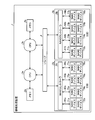
- FIG. 1 is a schematic configuration diagram of an information processing apparatus.
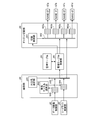
- FIG. 2 is a block diagram of the NAND controller according to the first embodiment.
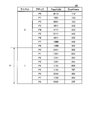
- FIG. 3 is a diagram illustrating an example of a management table.
- FIG. 4 is a diagram illustrating an example of a format of a signal input to the arbitration unit.
- FIG. 5 is a diagram illustrating the state of the management table and the address conversion table before execution of garbage collection.
- FIG. 6 is a diagram illustrating the state of the management table and the address conversion table after execution of garbage collection.
- FIG. 7 is a detailed block diagram relating to data writing in the arbitration unit and the channel switching unit.
- FIG. 8 is a time chart showing the output from each part of the NAND controller.
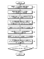
- FIG. 9 is a flowchart of data movement processing and processing of a write command from the CPU.
- FIG. 10 is a flowchart of the scrub process performed by the NAND controller according to the second embodiment.
- FIG. 11 is a block diagram of a NAND controller according to the third embodiment.
- FIG. 1 is a schematic configuration diagram of an information processing apparatus.
- the information processing apparatus 1 includes a plurality of memories 2a and 2b, a plurality of CPUs (Central Processing Units) 3a and 3b, an I / O (Input Output) hub 4, and a plurality of SSDs (Solid State Drives) 5a and 5b.
- the SSD 5a includes a NAND controller 6a and a plurality of NAND devices 71a to 78a.
- the SSD 5b includes a NAND controller 6b and a plurality of NAND devices 71b to 78b.
- the SSD 5b, the NAND controller 6b, and the plurality of NAND devices 71b to 78b perform the same functions as the SSD 5a, the NAND controller 6a, and the plurality of NAND devices 71a to 78a, and the description thereof is omitted. To do.
- the memories 2a and 2b are storage devices that store data used by the CPUs 3a and 3b for arithmetic processing.
- the CPUs 3a and 3b are arithmetic processing devices that perform various arithmetic processes using data stored in the memories 2a and 2b.
- the CPUs 3a and 3b use NUMA (Non-Uniform Memory Access) technology to acquire data stored in the memories 2a and 2b, and execute arithmetic processing using the acquired data.
- NUMA Non-Uniform Memory Access
- the CPUs 3a and 3b acquire data stored in the SSDs 5a and 5b via the I / O hub 4, and execute arithmetic processing using the acquired data. Specifically, the CPU 3a issues a data read request and a write request to the SSD 5a, and reads and writes data from each of the NAND devices 71a to 78a. For example, the CPU 3a issues a read request storing a logical address designating data to be read to the SSD 5a. In addition, the CPU 3a issues a write request in which a logical address that specifies a data write destination and data to be written are stored.
- the NAND device 71a is a nonvolatile memory that stores various data. More specifically, the NAND device 71a has a plurality of physical pages, which are data storage areas, and writes data in units of physical pages.
- the NAND device 71a has a plurality of physical blocks each having a plurality of physical pages, and erases data in units of blocks.
- one physical page has a storage capacity of, for example, 8 kilobytes
- one physical block has, for example, 128 physical pages.
- the NAND device 71a is connected to the NAND controller 6a through the transmission path 81a.
- the transmission path 81a connecting the NAND device 71a and the NAND controller 6a is called a channel.
- the transmission path 81a is referred to as a channel 81a.
- the NAND device 72a is connected to the NAND controller 6a through a channel 81a similar to the NAND device 71a.
- one channel 81a is shared by the NAND devices 71a and 72a.
- the number of NAND devices sharing one channel may be one or three or more.
- the channel 82a is shared by the NAND device 73a and the NAND device 74a.
- the channel 83a is shared by the NAND device 75a and the NAND device 76a.
- the channel 84a is shared by the NAND device 77a and the NAND device 78a.
- the NAND devices 71a to 78a are an example of “storage unit”.
- the NAND controller 6a accesses each of the NAND devices 71a to 78a, and reads and writes data. For example, the NAND controller 6a associates a logical address used when the CPUs 3a and 3b specify a storage area in which data is stored with a physical address indicating a storage area of the NAND devices 71a to 78a in which the data is stored. An address translation table.
- the NAND controller 6a When the NAND controller 6a receives the logical address together with the read request, the NAND controller 6a uses the address conversion table to identify the physical address associated with the logical address, and reads data from the storage area indicated by the identified physical address. . Thereafter, the NAND controller 6a transmits the read data to the CPU 3a via the I / O hub 4.
- the logical address that is the start address of each physical page is simply described as a logical address
- the physical address that is the start address of each physical page is simply described as a physical address.
- the CPU 3a or 3b issues a read request or a write request for the logical address that is the head address of each physical page.
- NAND controller 6 when the NAND controllers 6a and 6b are not distinguished, they are simply referred to as “NAND controller 6”. Further, when the NAND devices 71a to 78a and 71b to 78b are not distinguished, they are simply referred to as “NAND device 70”. When the CPUs 3a and 3b are not distinguished, they are simply referred to as “CPU3”. Further, when the channels 81a to 84a and 81b to 84b are not distinguished, they are simply referred to as “channel 80”.
- FIG. 2 is a block diagram of the NAND controller according to the first embodiment.
- the NAND controller 6 includes a movement target detection unit 61, a data movement control unit 62, a read / write control unit 63, an arbitration unit 64, a management table control unit 65, a channel switching unit 66, and a NAND-IF (Interface). ) 67a to 67d.
- NAND-IF67 when the NAND-IFs 67a to 67d are not distinguished, they are simply referred to as “NAND-IF67”.
- the NAND controller 6 according to the present embodiment has a management table 68 and an address conversion table 69.
- the management table 68 has a format shown in FIG.
- FIG. 3 is a diagram illustrating an example of a management table. As shown in FIG. 3, the management table 68 holds, for each block of each channel, information on whether each page included in the block is valid or invalid and the last update time.
- “PageValid” in the management table 68 is information indicating whether each page included in the block is valid or invalid. In FIG. 3, there are four pages in one block, and each page is represented by four bits. If the bit corresponding to a certain page is 0, it indicates that the page is an invalid page. If the bit corresponding to a certain page is 1, it indicates that the page is a valid page. “TimeStamp” represents the last update time of each page.
- the management table 68 is used, for example, for garbage collection, wear leveling, or detection of a write destination in a data write command from the CPU.
- the address conversion table 69 In the address conversion table 69, the correspondence between the logical address designated by the CPU 3 and the physical address in the NAND device 71 is registered.
- the address conversion table 69 holds, as physical address information, a combination of information on a page having the physical address and information on a block including the page. Further, the address conversion table 69 holds information on the channel 80 for accessing the NAND device 70 including the page having the physical address as information on the physical address.
- the address conversion table 69 is used when the read / write control unit 63 acquires a physical address corresponding to a logical address designated by the CPU 3.
- the management table control unit 65 when data is written to the NAND device 70, the logical address designated as the storage location of the data to be written by the management table control unit 65 corresponds to the physical address of the write destination. To be updated. In this case, in the address conversion table 69, the management data control unit 65 deletes the correspondence between the physical address and the logical address in which the data to be written is read.
- the movement target detection unit 61 transmits a search request for the management table 68 to the management table control unit 65 in response to an instruction from the software or an internal timer. Thereafter, when executing the garbage collection or wear leveling, the movement target detection unit 61 receives, from the management table control unit 65, an input of information on the execution target page as a request response.
- the movement target detection unit 61 acquires, for example, information on the physical block in which the page exists, information on the physical address of the page, and information on the channel 80 for accessing the page as information on the execution target page. .
- the movement target detection unit 61 notifies the data movement control unit 62 of information on the execution target page. Furthermore, the movement target detection unit 61 notifies the data movement control unit 62 of information indicating the type of processing to be executed, that is, whether garbage collection or wear leveling is executed. Accordingly, the movement target detection unit 61 instructs the data movement control unit 62 to sequentially move the data of the execution target page to a new physical block. Thereafter, the movement target detection unit 61 receives a garbage collection or wear leveling process completion response from the data movement control unit 62 and ends the garbage collection or wear leveling process.
- the data movement control unit 62 receives information on the page to be executed and information indicating which process of garbage collection or wear leveling is to be executed from the movement target detection unit 61.
- the data movement control unit 62 sequentially outputs a data read command from each execution target page notified by the movement target detection unit 61 to the arbitration unit 64. Thereafter, the data movement control unit 62 receives input of data read from the designated page from the arbitration unit 64. Then, the data movement control unit 62 temporarily stores the received data in association with the information of the movement target page that is the reading source.
- the data movement control unit 62 outputs the temporarily stored data to the arbitration unit 64 together with information on the channel 80 used for reading and a write command.
- the channel 80 used for reading is the channel 80 for accessing the NAND device 70 having the page to be moved from which data is read.
- the data movement control unit 62 receives a response of the completion of the garbage collection or wear leveling process from the arbitration unit 64. Then, the data movement control unit 62 transmits a response to the completion of garbage collection or wear leveling processing to the movement target detection unit 61.
- FIG. 4 is a diagram illustrating an example of a format of a signal input to the arbitration unit.
- the signal from the data movement control unit 62 but also the signal input from the read / write control unit 63 to the arbitration unit 64 has the format shown in FIG.
- a signal input from the data movement control unit 62 to the arbitration unit 64 includes an instruction type 101, a logical address 102, a physical address 103, a data movement control instruction number 104, and a management table in the header part.
- a search channel 105 is stored.
- the signal input from the data movement control unit 62 to the arbitration unit 64 stores the data 106 and the data error correction bit 107 in the data unit.
- the instruction type 101 information indicating any one of writing or reading instructed by the CPU 3, garbage collection, or wear leveling writing or reading is stored.
- the logical address 102 stores a logical address to be processed in the case of a write or read command from the CPU 3.
- the physical address 103 is empty when it is input to the arbitration unit 64.
- the data movement control instruction number stores a number indicating any one of garbage collection, wear leveling, and scrubbing.
- the search channel 105 of the management table stores the number of the channel 80 used when searching for a page to be processed.
- the data 106 stores data to be written.
- the data error correction bit 107 stores information for error correction of data to be written.
- the information for error correction is, for example, an error detection code of ECC (Error Check and Correct).
- the data movement control unit 62 stores information indicating either garbage collection or wear leveling in the command type 101. Further, the data movement control unit 62 stores the physical address of the movement target page in the physical address 103. The data movement control unit 62 stores a number indicating either garbage collection or wear leveling in the number 104 of the data movement control instruction. Further, the data movement control unit 62 stores information of the channel 80 for accessing the NAND device 70 having the page to be moved in the search channel 105 of the management table. In this case, the data movement control unit 62 stores nothing in the logical address 102, the data 106, and the error correction bit 107 of the data.
- the data movement control unit 62 stores information indicating either garbage collection or wear leveling in the command type 101. In this case, the data movement control unit 62 leaves the logical address 102 empty. At this time, the page to which data is written has not been determined, so the data movement control unit 62 leaves the physical address 103 empty.
- the data movement control unit 62 stores a number indicating either garbage collection or wear leveling in the number 104 of the data movement control instruction. Further, the data movement control unit 62 stores the information of the channel 80 used for reading in the search channel 105 of the management table. Further, the data movement control unit 62 stores data to be written in the data 106. Further, the data movement control unit 62 calculates information for error correction of the data to be written, and stores the calculated error correction information in the error correction bit 107 of the data.
- the data movement control unit 62 is an example of a “data movement unit”.
- the read / write control unit 63 receives an input of a data write command for the NAND device 70 from the CPU 3. Then, the read / write control unit 63 acquires a physical address corresponding to the logical address designated by the write command from the address conversion table 69. Then, the read / write unit 63 outputs a write command using the acquired physical address as a read address to the arbitrating unit 64.
- the read / write control unit 63 outputs a write command to the arbitration unit 64 without specifying a read address.
- the read / write control unit 63 receives a write completion response from the arbitration unit 64. Then, the read / write control unit 63 returns a write completion response to the CPU 3.
- the read / write control unit 63 receives an input of a read command for the NAND device 70 from the CPU 3. Then, the read / write control unit 63 acquires from the address conversion table 69 a physical address corresponding to the logical address designated by the read command. Then, the read / write control unit 63 outputs a read command using the acquired physical address as a read address to the arbitration unit 64.
- the read / write control unit 63 receives input of the read data from the arbitration unit 64. Then, the read / write control unit 63 returns the received response to the CPU 3 as a response to the read command.
- the read / write control unit 63 also sends a write command or a read command to the arbitration unit 64 using a signal having the format shown in FIG.
- the read / write control unit 63 stores information indicating that it is a write command from the CPU 3 in the command type 101. Further, the read / write control unit 63 stores the logical address designated by the write command in the logical address 102. Further, the read / write control unit 63 stores, in the physical address 103, the physical address of the page from which data is read when the write command is data update. On the other hand, when the write command is not the data update but the first write, the read / write control unit 63 leaves the physical address 103 empty. Furthermore, the read / write control unit 63 leaves the command number for data movement control empty.
- the read / write control unit 63 since the channel 80 for searching for the write destination page is not determined, the read / write control unit 63 leaves the search channel 105 of the management table empty. Further, the read / write control unit 63 stores data to be written in the data 106. Further, the read / write control unit 63 calculates error correction information from the data, and stores the calculated error correction information in the error correction bit 107 of the data.
- the read / write control unit 63 stores information indicating that it is a read command from the CPU 3 in the command type 101. Further, the read / write control unit 63 stores the logical address designated by the read command in the logical address 102. The read / write control unit 63 stores the physical address of the page from which data is read out in the physical address 103. In this case, the read / write control unit 63 leaves the command number for data movement control empty. Further, the read / write control unit 63 stores the channel 80 used for reading in the search channel 105 of the management table. In the case of a read command, the read / write control unit 63 stores nothing in the data 106 and the error correction bit 107 of the data. The read / write control unit 63 is an example of a “write execution unit”.
- the arbitration unit 64 arbitrates the read command and the write command from the data movement control unit 62 and the read / write control unit 63, and outputs them to the management table control unit and the switch element 662.
- the arbitration unit 64 sequentially receives a page read command using a signal having the format of FIG. 4 from the data movement control unit 62 when performing garbage collection or wear leveling. Then, the arbitrating unit 64 instructs the channel switching unit 66 to read data from the page specified by the read command. Thereafter, the arbitrating unit 64 receives the read data from the channel switching unit 66. Next, the arbitrating unit 64 outputs the read data to the data movement control unit 62.
- the arbitration unit 64 receives a write command using a signal having the format of FIG. 4 from the data control unit 62. As a result, the arbitration unit 64 acquires the information about the channel 80 used for reading and the data to be written together with the write instruction.
- the arbitrating unit 64 instructs the management table control unit 65 to specify a block having a spare block that exists in the NAND device 70 connected to the channel 80 used for reading. Further, the arbitrating unit 64 outputs the data to be written to the channel switching unit 66. After that, the arbitrating unit 64 receives a data write completion response from the channel switching unit 66.
- the arbitration unit 64 performs the above processing on all the instructed pages read by the data movement control unit 62. Thereafter, the arbitration unit 64 notifies the data movement control unit 62 of a response of completion of garbage collection or wear leveling processing.
- the arbitration unit 64 receives a data write command or read command using a signal having a format shown in FIG. 4 from the read / write control unit 63.
- the arbitration unit 64 instructs the channel switching unit 66 to read data from the physical address specified by the write command. Thereafter, the arbitrating unit 64 acquires the read data from the channel switching unit 66. Then, the arbitrating unit 64 merges the read data and the data received from the read / write control unit 63 to update the data.
- the arbitration unit 64 determines whether or not an execution command for garbage collection or wear leveling has been received.
- garbage collection and the wear leveling are not distinguished, they are referred to as “data movement processing”.
- the arbitration unit 64 acquires, from the write command, the channel 80 for accessing the NAND device 70 having the page to be moved in the data movement process command. Then, the arbitrating unit 64 notifies the management table control unit 65 of an instruction to select a free page from the channel 80 other than the acquired channel 80. Further, the arbitrating unit 64 outputs the data to the channel switching unit 66. After that, the arbitrating unit 64 receives a data write completion response from the channel switching unit 66. Then, the arbitrating unit 64 transmits a data write completion response to the read / write control unit 63.
- the arbitrating unit 64 notifies the management table control unit 65 of an instruction to select an empty page from all the channels 80. Further, the arbitrating unit 64 outputs the data to the channel switching unit 66. Thereafter, the arbitrating unit 64 transmits a write completion response to the read / write control unit 63. After that, the arbitrating unit 64 receives a data write completion response from the channel switching unit 66. Then, the arbitrating unit 64 transmits a data write completion response to the read / write control unit 63.
- the arbitration unit 64 instructs the channel switching unit 66 to read data from the physical address specified by the read command. Thereafter, the arbitrating unit 64 acquires the read data from the channel switching unit 66. Then, the arbitration unit 64 transmits the read data to the read / write control unit 63 as a response.
- the management table control unit 65 sends, from the arbitration unit 64, a specific instruction for a block having a spare block that exists in the NAND device 70 connected to the channel 80 used for reading at the time of data writing. receive. Then, the management table control unit 65 searches the management table 68 and identifies a block having a spare block from the NAND device 70 connected to the channel 80 used for reading. Further, the management table control unit 65 acquires the physical address of the page to which data is written in the specified physical block from the management table 68. Then, the management table control unit 65 outputs information on the channel 80 used for reading and the acquired physical address to the channel switching unit 66.
- the management table control unit 65 specifies a block having a spare block from among the blocks included in the channel 80 whose identification number is 1. That is, the management table control unit 65 searches the range P and identifies a block having a spare block.
- the management table control unit 65 updates the address conversion table 69 so that the logical address of the movement target page corresponds to the physical address of the movement destination page.
- the management table control unit 65 selects a free page from a channel 80 other than the channel 80 used in the data movement processing when writing data.
- An instruction to perform is received from the arbitration unit 64. Then, using the management table 68, the management table control unit 65 selects a free page from the management table 68 from among the NAND devices 70 connected to the channels 80 other than the channel 80 used in the data movement process.
- the management table control unit 65 selects a free page from the blocks included in the channel 80 other than the channel 80 whose identification number is 1. In other words, the management table control unit 65 searches outside the range P and selects an empty page.
- the management table control unit 65 outputs information on the channel 80 used for writing and the physical address of the page to be written to the channel switching unit 66 other than the channel 80 used in the data movement process.
- management table control unit 65 updates the address conversion table 69 so that the logical address indicating the page in which the written data is stored corresponds to the physical address of the write destination page.
- FIG. 5 is a diagram illustrating the state of the management table and the address conversion table before execution of garbage collection.
- FIG. 6 is a diagram illustrating the state of the management table and the address conversion table after execution of garbage collection.
- the management table 68 and the address conversion table 69 in FIG. 5 represent the state before execution of garbage collection.
- a table 701 represents the state of a page included in the NAND device 70 connected to the channels # 0 and # 1.
- a crossed page in the table 701 represents an invalid page.
- the management table control unit 65 receives a search request for the management table 68 from the movement target detection unit 61 and detects the state of invalid pages from the first block to the last block for each channel of the management table 68. Then, the management table control unit 65 selects a block that satisfies a predetermined condition as a target block for garbage collection. In FIG. 5, the management table control unit 65 selects the block P2 of the channel # 0 represented by the row 681 as a garbage collection target block.
- the management table control unit 65 selects a block having a spare block from the channel # 0, which is the same channel 80 as the channel 80 used for reading, as a writing destination block when writing data. That is, the management table control unit 65 searches for a block included in the range Q of the management table 68 and selects a block having a spare block. In this embodiment, the management table control unit 65 selects the block P8 of channel # 0. As described above, in this embodiment, when searching for a write destination block, only the range of one channel 80 is set as a search target.
- the management table control unit 65 selects the page 711 of the block P2 of the channel # 0 as a movement target.
- the physical address of each page is represented by a combination of a block number and a page number.
- the physical address of page 711 is P2-3.
- a page 711 corresponds to the logical address L3.
- the management table control unit 65 moves the data of the page 711 to the page 712 of the selected block P8.
- the physical address of page 712 is P8-0.
- the management table control unit 65 invalidates the page 711 of the block P2 in the row 681 of the management table 68. Furthermore, the management table control unit 65 updates the update date and time of the block P2 in the row 681 of the management table 68.
- the management table control unit 65 changes the information of the physical address 691 corresponding to the logical address L3 of the address conversion table 69 to the information of the write destination page 712. Specifically, the management table control unit 65 sets the channel 80 corresponding to the logical address L3 to channel # 0, and sets the block and page information representing the physical address to P8-0. Thus, the update of the management table 68 and the address conversion table 69 at the time of writing in the data movement process is completed.
- the management table control unit 65 receives an instruction to select an empty page from all the channels 80 from the arbitration unit 64 when writing data. . Then, the management table control unit 65 uses the management table 68 to select a free page from the NAND devices 70 connected to all the channels 80. Thereafter, the management table control unit 65 outputs the channel 80 information used for writing and the physical address of the write destination page to the channel switching unit 66.
- management table control unit 65 updates the address conversion table 69 so that the logical address indicating the page in which the written data is stored corresponds to the physical address of the write destination page.
- the management table control unit 65 is an example of a “selection unit”.
- the channel switching unit 66 first receives a data read command from the arbitration unit 64. Next, the channel switching unit 66 switches the path to the NAND-IF 67 connected to the channel 80 for accessing the NAND device 70 having the page specified by the read command. Then, the channel switching unit 66 outputs a read command including the data received from the arbitration unit 64 and information on the page to be moved to the NAND-IF 67.
- the channel switching unit 66 receives the read data input from the NAND-IF 67. Then, the channel switching unit 66 transmits the received data to the arbitration unit 64.
- the channel switching unit 66 receives input of data to be written from the arbitrating unit 64. Further, the channel switching unit 66 receives from the management table control unit 65 the information of the channel 80 used for reading and the physical address of the write destination page. The channel switching unit 66 switches the path to the NAND-IF 67 connected to the channel 80 used for reading. Then, the channel switching unit 66 outputs a write command including the data received from the arbitration unit 64 and information on the write destination page to the NAND-IF 67.
- the channel switching unit 66 receives a data write completion response from the NAND-IF 67.
- the channel switching unit 66 then transmits a data write completion response to the arbitration unit 64.
- the channel switching unit 66 receives input of data to be written from the arbitration unit 64. Further, the channel switching unit 66 receives from the management table control unit 65 the input of the channel 80 information used for writing and the physical address of the page to be written. Here, if a data movement processing command has been received, the channel switching unit 66 acquires information on channels 80 other than the channel 80 used for data movement processing as information on the channel 80 used for writing. Then, the channel switching unit 66 switches the path to the NAND-IF 67 connected to the channel 80 used for writing. Thereafter, the channel switching unit 66 outputs a write command including the data received from the arbitration unit 64 and information of the write destination page to the NAND-IF 67.
- the channel switching unit 66 receives a data write completion response from the NAND-IF 67.
- the channel switching unit 66 then transmits a data write completion response to the arbitration unit 64.
- the channel switching unit 66 receives input of data to be read from the arbitration unit 64. Further, the channel switching unit 66 receives from the management table control unit 65 the information of the channel 80 used for reading and the physical address of the page to be read. Then, the channel switching unit 66 switches the path to the NAND-IF 67 connected to the channel 80 used for reading. After that, the channel switching unit 66 outputs a read command including information on the page to be read to the NAND-IF 67.
- the channel switching unit 66 receives the read data from the NAND-IF 67. Then, the channel switching unit 66 outputs the read data to the arbitration unit 64.
- NAND-IFs 67 are connected to different channels 80, respectively. That is, the NAND-IF 67 performs writing and reading with respect to different NAND devices 70.
- the NAND-IF 67 receives an input of a data read command including the physical address of the page to be read from the channel switching unit 66. Next, the NAND-IF 67 reads data from the page at the physical address specified by the read command. Then, the NAND-IF 67 outputs the read data to the arbitration unit 64.
- the NAND-IF 67 receives from the channel switching unit 66 an input of a data write command including the data to be written and the physical address of the write destination page. Next, the NAND-IF 67 writes the received data to the page at the physical address specified by the write command. Then, the NAND-IF 67 outputs a write completion response to the arbitration unit 64.
- the NAND-IF 67 writes data using the channel 80 connected to the NAND device 70 having the page to be moved. That is, in the garbage collection or wear leveling, the read data is written to another block using the same channel 80 as the channel 80 used for reading. That is, in this embodiment, the channel 80 used for reading and the channel 80 used for writing coincide in garbage collection or wear leveling.
- the NAND-IF 67 When the NAND-IF 67 receives a write command from the CPU 3 while receiving an execution command for data movement processing, the NAND-IF 67 uses a channel 80 other than the channel 80 used for the data movement processing. Write. When the write instruction from the CPU 3 is received without receiving the execution instruction for the data movement process, the NAND-IF 67 selects an empty page without the limitation of the channel 80 and writes the data.
- the NAND-IF 67 writes data instructed to be written by the CPU 3 using a channel 80 other than the channel 80 used for data movement processing. That is, the channel 80 used for writing data instructed to be written by the CPU 3 does not compete with the channel 80 used for data movement processing.
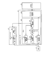
- FIG. 7 is a detailed block diagram relating to data writing in the arbitration unit and the channel switching unit.
- the arbitration unit 64 includes an output source selection unit 641, a search channel selection unit 642, FIFO (Fast In Fast Out) buffers 643 and 644, and a switch element 645.
- the channel switching unit 66 includes a switching control unit 661, a switch element 662, and FIFO buffers 663a to 663d.
- the FIFO buffer 643 has a FIFO queue.
- the FIFO buffer 643 receives an input of a data write command in the data movement process from the data movement control unit 62.
- channel 80 information used for reading is stored as channel information used for writing.
- the FIFO buffer 643 outputs a write destination page selection instruction to the management table control unit 65 via the switch element 645 in order from the oldest write command, together with information on the channel 80 used for reading. At the same time, the FIFO buffer 643 outputs the data to be written to the channel switching unit 66 via the switch element 645.
- the FIFO buffer 644 has a FIFO queue.
- the FIFO buffer 644 receives an input of a data write command from the CPU 3 from the read / write control unit 63. Furthermore, the FIFO buffer 644 receives from the search channel selection unit 642 an input of search channel information to be searched for the write destination page.
- This search channel information is information indicating a channel 80 other than the channel 80 used for writing in the data movement processing performed in parallel.
- the FIFO buffer 644 outputs a selection instruction of a page to be written to the management table control unit 65 via the switch element 645 in order from the oldest write command, together with search channel information. At the same time, the FIFO buffer 644 outputs data to be written to the channel switching unit 66 via the switch element 645.
- the search channel selection unit 642 acquires information on the channel 80 used for writing, that is, information on the channel 80 used for reading, from the data write command in the leading data movement process stored in the FIFO buffer 643. Then, the search channel selection unit 642 outputs information on the channel 80 used for writing data in the migration process to the FIFO buffer 644 as information on the search channel to be searched for the write destination page.
- the output source selection unit 641 switches the switch elements 645 in a predetermined order so that the output from the data movement control unit 62 and the output from the read / write control unit 63 are evenly output from the switch element 645.
- the output source selection unit 641 alternately selects the output of the FIFO buffer 643 and the output of the FIFO buffer 644 and switches them in order so as to be output from the switch element 645.
- the switch element 645 receives the switching control from the switching control unit 661, and switches the path so that any one of the outputs from the FIFO buffers 643 and 644 is output from the management table control unit 65 and the switching element 662.
- the management table control unit 65 receives, from the FIFO buffer 643 via the switch element 645, an input of a write destination page selection instruction together with information on the channel 80 used for reading. Next, the management table control unit 65 extracts a spare block from the NAND device 70 connected to the channel 80 used for reading, and selects an empty page of the extracted spare block as a write destination page. Then, the management table control unit 65 outputs information on the selected write destination page to the switching control unit 661. Further, the management table control unit 65 outputs the information of the selected write destination page to the switch element 645.
- the management table control unit 65 receives an input of a selection instruction of a write destination page from the FIFO buffer 644 through the switch element 645 together with the search channel information. Specifically, the management table control unit 65 acquires information on channels 80 other than the channel 80 used for writing in the data movement processing performed in parallel as information on search channels.
- the management table control unit 65 selects a free page as a write destination page from the NAND devices 70 connected to the channels 80 other than the channel 80 used for writing in the data movement processing performed in parallel. Then, the management table control unit 65 outputs information on the selected write destination page to the switching control unit 661. Further, the management table control unit 65 outputs the information of the selected write destination page to the switch element 645.
- the switching control unit 661 receives from the management table control unit 65 an input of information of a write destination page in the data movement process. Then, the switching control unit 661 switches the switch element 643 so that the output from the management table control unit 65 and the switch element 645 is sent to the channel 80 connected to the NAND device 70 having the received write destination page.
- the switching control unit 661 receives from the management table control unit 65 input of information on the write destination page in the write command from the CPU 3. Then, the switching control unit 661 switches the switch element 662 so that the output from the management table control unit 65 and the switch element 645 is sent to the channel 80 connected to the NAND device 70 having the received write destination page.
- the switch element 645 receives the switching control from the switching control unit 661, and switches the path so that the output from the management table control unit 65 and the switch element 645 is input to any of the FIFO buffers 663a to 663d.
- the FIFO buffers 663a to 663d have a FIFO queue.
- the FIFO buffers 663a to 663d are connected to the NAND-IFs 67a to 67d, respectively. Since all of the FIFO buffers 663a to 663d have the same function, the FIFO buffers 663a to 663d are hereinafter referred to as “FIFO buffers 663” without distinction.
- the FIFO buffer 663 receives input of information and data of a write destination page via the switch element 662 when the switch element 662 switches the path to connect to itself. Specifically, the FIFO buffer 663 receives input of information of a write destination page from the management table control unit 65. In the case of data movement processing, the FIFO buffer 663 receives data input from the data movement control unit 62. In the case of a write command from the CPU 3, the FIFO buffer 663 receives data input from the read / write control unit 63.
- the FIFO buffer 663 outputs the received write destination page information and write target data to the connection destination NAND-IF 67.
- FIG. 8 is a time chart showing the output from each part of the NAND controller.
- the case where there are four channels # 0 to # 3 as the channel 80 will be described.
- the case where the data stored in the page of the NAND device 70 connected to channel # 0 is the data to be moved will be described as the data movement process.
- a chart 201 in FIG. 8 represents an output from the data movement control unit 62 to the arbitration unit 64.
- a chart 202 represents an output from the read / write control unit 63 to the arbitration unit 64.
- a chart 203 represents an output from the arbitration unit 64 to the management table control unit 65.
- a chart 204 represents an output from the management table control unit 65 to the channel switching unit 66.
- a chart 205 represents an output from the channel switching unit 66 to the NAND-IF 67 connected to the channel # 0.
- a chart 206 represents an output from the channel switching unit 66 to the NAND-IF 67 connected to the channel # 1.
- a chart 207 represents an output from the channel switching unit 66 to the NAND-IF 67 connected to the channel # 2.
- a chart 208 represents an output from the channel switching unit 66 to the NAND-IF 67 connected to the channel # 3.
- the horizontal axis in FIG. 8 represents the passage of time.
- Each square described in each of the charts 201 to 208 represents an output signal, and a signal generation source is described in the upper part of the output signal.
- a generation source here, there is a garbage collection (GC) or CPU3.
- GC garbage collection
- the contents of processing and the order of processing are described in the middle of the output signal.
- the contents of the process include a read process (Read) and a write process (Write).
- the order of processing is represented by the order of numbers in parentheses following the content of the processing.
- the number of the channel 80 to be processed is described in the lower part of the output signal. For example, “ch0” represents channel # 0.
- the data movement control unit 62 outputs to the arbitration unit 64 a signal 211 in which the processing target channel 80 is channel # 0 in response to the garbage collection zeroth read command.
- the data movement control unit 62 outputs to the arbitration unit 64 a signal 212 in which the channel 80 to be processed is channel # 0 in response to the first garbage collection read command.
- the data movement control unit 62 outputs a signal 213, which is the zeroth write command for garbage collection, to the arbitration unit 64.
- the data movement control unit 62 sets the processing target channel 80 in the garbage collection writing to be the same as the channel 80 used for reading. Therefore, the processing target channel 80 in the signal 211 is channel # 0.
- the data movement control unit 62 outputs to the arbitration unit 64 a signal 214 that is the first garbage collection write command and the processing target channel 80 is channel # 0.
- the arbitration unit 64 outputs the signal 211 received from the data movement control unit 62 to the management table control unit 65.
- the arbitrating unit 64 outputs the signal 212 received from the data movement control unit 62 to the management table control unit 65.
- the management table control unit 65 outputs the signal 211 received from the arbitration unit 64 to the channel switching unit 66.
- the management table control unit 65 outputs the signal 212 received from the arbitration unit 64 to the channel switching unit 66.
- the channel switching unit 66 outputs to the NAND-IF 67 connected to the channel # 0 that is the processing target channel 80 indicated by the signal 211 received from the management table control unit 65. Thereafter, the NAND-IF 67 writes the data corresponding to the signal 211 to the NAND device 70 via the channel # 0. Further, the channel switching unit 66 outputs to the NAND-IF 67 connected to the channel # 0 that is the channel 80 to be processed indicated by the signal 212 received from the management table control unit 65. Thereafter, the NAND-IF 67 writes the data corresponding to the signal 212 to the NAND device 70 via the channel # 0.
- the read / write control unit 63 outputs to the arbitration unit 64 a signal 221 in which the channel 80 to be processed is channel # 0 in response to the 0th read command from the CPU 3.
- the read / write control unit 63 outputs to the arbitration unit 64 a signal 212 in which the channel 80 to be processed is channel # 1 in response to the first read command from the CPU 3.
- the data movement control unit 62 outputs to the arbitration unit 64 a signal 213 in which the channel 80 to be processed is channel # 0 in response to the 0th write command for garbage collection.
- the read / write control unit 63 outputs to the arbitration unit 64 a signal 223 in which the channel 80 to be processed is not determined by the 0th write command from the CPU 3.
- the data movement control unit 62 outputs to the arbitration unit 64 a signal 214 in which the processing target channel 80 is channel # 0 in response to the first garbage collection write command.
- the read / write control unit 63 outputs to the arbitration unit 64 a signal 224 in which the channel 80 to be processed is undecided by the first write command from the CPU 3.
- the read / write control unit 63 outputs to the arbitration unit 64 a signal 225 in which the channel 80 to be processed is channel # 1 by the second write command from the CPU 3.
- the arbitration unit 64 outputs the signal 221 received from the read / write control unit 63 to the management table control unit 65 and the channel switching unit 66 as shown in the chart 203. Thereafter, the arbitrating unit 64 alternately outputs signals 222 to 225 that are outputs from the read / write control unit 63 and signals 213 to 214 that are output from the data movement control unit 62 to the management table control unit 65.
- the arbitration unit 64 selects the channel 80 for searching for the page to which the signal 223 is written from the channels 80 other than the channel # 0, which is the channel 80 to be processed by the signal 213 output immediately before.
- the arbitrating unit 64 selects channel # 1 as the channel 80 to be processed by the signal 223.
- the arbitration unit 64 selects the channel 80 for searching for the page to which the signal 224 is written from the channels 80 other than the channel # 0 that is the channel 80 to be processed by the signal 214 output immediately before.
- the arbitrating unit 64 selects channel # 1 as the channel 80 to be processed by the signal 224.
- the management table control unit 68 receives the signals 222 to 225 and 213 to 214 from the arbitration unit 64 as shown in the chart 204. Then, the management table control unit 68 selects an empty page from the NAND devices 70 connected to the processing target channel 80 indicated by each signal. Then, the management table control unit 68 outputs signals 222 to 225 and 213 to 214 to the channel switching unit 66 together with information on the selected empty page.
- the channel switching unit 66 outputs the signal received from the management table control unit 65 to the NAND-IF 67 connected to the processing target channel 80 of the signal. Specifically, as shown in chart 205, channel switching unit 66 outputs signals 211, 213, and 214 to NAND-IF 67 connected to channel # 0. Further, as shown in chart 206, channel switching unit 66 outputs signals 222 to 225 to NAND-IF 67 connected to channel # 1.
- the channel switching unit 66 does not output signals to the NAND-IF 67 connected to the channels # 2 and # 3.
- the information processing apparatus 1 can reduce the waiting time of the data movement process and the process for the write command from the CPU 3, and can improve the processing efficiency.
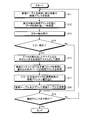
- FIG. 9 is a flowchart of data movement processing and processing of a write command from the CPU.
- a write command is input from the CPU 3 in parallel with the data movement process.
- the management table control unit 65 receives the request from the movement target detection unit 61, searches the management table 68, and selects the physical address of the page to be moved. Then, the data movement control unit 62 acquires the physical address of the page to be moved selected by the management table control unit 65 (step S1).
- the data movement control unit 62 outputs a data read command from the movement target page to the arbitration unit 64.
- the arbitration unit 64 reads data from the NAND device 70 based on the physical address to be moved, and outputs the data to the data movement control unit 62.
- the data movement control unit 62 temporarily stores the read data (step S2).
- the data movement control unit 62 instructs the arbitration unit 64 to write the read data.
- the arbitration unit 64 notifies the management table control unit 65 of the channel 80 from which the data has been read as a search channel used for searching for the write destination page (step S3).
- the arbitration unit 64 receives an input of a write command from the CPU 3 from the read / write control unit 63. Then, the arbitrating unit 64 notifies the management table control unit 65 of channels 80 other than the channel 80 used for writing data movement processing as the channel 80 used for writing data designated by the CPU 3 (step S4).
- the management table control unit 65 searches the management table 68 for a spare block using the channel 80 notified from the arbitration unit 64 as a search channel, and sets the spare block of the search result as a write destination page (step S5).
- the channel switching unit 66 transmits the data temporarily stored by the data movement control unit 62 to the NAND-IF 67 connected to the page selected by the arbitration unit 64.
- the NAND-IF 67 writes data in the spare block of the search result of the NAND device 70 using the channel 80 used for reading (step S6).
- the management table control unit 65 updates the management table 68 and the address conversion table 69 (step S7).
- the management table control unit 65 searches for a page to which data is written in response to a write command from the CPU 3, using a channel 80 other than the channel 80 used for writing in the data movement process as a search channel. Then, the channel switching unit 66 transmits data to the NAND-IF 67 connected to the write destination page selected by the management table control unit 65. The NAND-IF 67 writes data to the search result page of the NAND device 70 using the channel 80 other than the channel 80 used for writing the data movement process (step S8).
- the movement target detection unit 61 determines whether or not the data movement process has been executed for all the blocks in the management table 68 (step S9). If there is a block for which the data movement process has not been completed (No at Step S9), the movement target detection unit 61 returns to Step S1.
- step S9 Yes
- the NAND controller 6 ends the data movement process.
- the NAND controller uses a channel different from the channel used in the data movement process for processing the write command from the CPU. Therefore, the competition between the channel used in the data movement process and the channel used for the write command from the CPU can be suppressed, and the processing efficiency can be improved.
- the channel used for reading and the channel used for writing are matched in the data movement processing, and the other channels are used for processing of the CPU write command.
- the channel selection method is not limited to this as long as the channel used for data movement processing is different from the channel used for CPU write instruction processing. For example, if the number of channels is sufficient, a channel used for writing in the data movement process may be appropriately selected, and a channel other than the channel used for the data movement process may be used for processing the CPU write command.
- Example 2 will be described.
- the channel used for reading data and the channel used for writing are different in executing scrub for error detection and correction. Therefore, the function of each part in the scrub will be mainly described below.
- An information processing apparatus and a NAND controller according to this embodiment are also shown in FIGS. In the following, description of the same functions as those of the first embodiment will be omitted.
- the movement target detection unit 61 transmits a search request for the management table 68 to the management table control unit 65 in response to an instruction from the software or an internal timer. Thereafter, when executing the scrub, the movement target detection unit 61 receives an input of information on the execution target page from the management table control unit 65 as a request response. The movement target detection unit 61 notifies the data movement control unit 62 of the physical address of the page to be scrubbed. Further, the movement target detection unit 61 notifies the data movement control unit 62 of a scrub execution instruction.
- the data movement control unit 62 receives an input of a physical address of a page on which scrubbing is performed from the movement target detection unit 61. Then, the data movement control unit 62 outputs a data read command together with the physical address to the arbitration unit 64. Thereafter, the data movement control unit 62 receives the read data from the arbitration unit 64. Then, the data movement control unit 62 temporarily stores the read data.
- the data movement control unit 62 detects an error in the stored data. If no error is detected, the data movement control unit 62 discards the read data and reads data from the next physical address.
- the data movement control unit 62 performs error correction on the data in which the error is detected. Next, the data movement control unit 62 selects a channel 80 other than the channel 80 used for reading from the management table 68. Then, the data movement control unit 62 outputs a data write command after error correction to the selected channel 80 to the arbitration unit 64.
- the arbitration unit 64 outputs the physical address and data read command received from the data movement control unit 62 to the channel switching unit 66. Thereafter, the arbitrating unit 64 receives the read data from the channel switching unit 66. Then, the arbitration unit 64 outputs the read data to the data movement control unit 62.
- the arbitration unit 64 receives an input of a data write command after error correction to the channel 80 selected by the data movement control unit 62. Then, the arbitrating unit 64 outputs to the management table control unit 65 a command to write data after error correction to the channel 80 selected by the data movement control unit 62. Further, the arbitrating unit 64 outputs the data after error correction to the channel switching unit 66.
- the management table control unit 65 receives from the arbitration unit 64 an input of a data write command after error correction to the channel 80 selected by the data movement control unit 62. Then, the management table control unit 65 selects a write destination page from the pages of the NAND device 70 connected to the designated channel 80. Next, the management table control unit 65 notifies the channel switching unit 66 of the physical address of the selected page. Thereafter, the management table control unit 65 updates the management table 68 and the address conversion table 69.
- the channel switching unit 66 outputs a physical address and data read command to the NAND-IF 67 connected to the physical address designated by the arbitration unit 64. Thereafter, the channel switching unit 66 receives the read data from the NAND-IF 67. Then, the channel switching unit 66 outputs the read data to the arbitration unit 64.
- the channel switching unit 66 receives from the management table control unit 65 the input of the physical address of the page to which the error-corrected data is written. Further, the channel switching unit 66 receives data input after error correction from the arbitrating unit 64. Then, the channel switching unit 66 writes the write command to the physical address received from the management table control unit 65 of the data after error correction to the NAND device 70 connected to the page having the physical address.
- the NAND-IF 67 receives a read command from the channel switching unit 66, reads data from the designated physical address of the NAND device 70, and outputs the data to the channel switching unit 66.
- the NAND-IF 67 receives a write command from the channel switching unit 66 and writes data to a designated physical address of the NAND device 70.
- the NAND-IF 67 for writing data is connected to a channel 80 different from the channel 80 used for reading. Therefore, data writing is performed using a channel 80 different from data reading.
- FIG. 10 is a flowchart of the scrub process performed by the NAND controller according to the second embodiment.
- the management table control unit 65 receives the request from the movement target detection unit 61, searches the management table 68, and selects the physical address of the scrub execution target page. Then, the data movement control unit 62 acquires the physical address of the execution target page selected by the management table control unit 65 (step S11).
- the data movement control unit 62 reads and temporarily stores data from the designated physical address in the NAND device 70 via the arbitration unit 64, the channel switching unit 66, and the NAND-IF 67 (step S12).
- the data movement control unit 62 performs error detection on the stored data (step S13).
- the data movement control unit 62 determines whether or not an error has occurred in the read data (step S14). When no error has occurred (No at Step S14), the NAND controller 6 proceeds to Step S19.
- step S14 when an error has occurred (step S14: affirmative), the data movement control unit 62 selects a channel 80 different from the channel 80 from which the data was read from the management table 68 as a search channel (step S15). Then, the data movement control unit 62 performs error correction and notifies the arbitration unit 64 of a data write command after error correction using the search channel 80.
- the arbitration unit 64 instructs the management table control unit 65 to select a spare block from the search channel.
- the management table control unit 65 searches for a spare block in the search channel from the management table 68, and obtains the physical address of the page to be written (step S16). Then, the management table control unit 65 notifies the acquired physical address to the channel switching unit 66.
- the channel switching unit 66 outputs the error correction data write command received from the arbitration unit 64 to the NAND-IF 67 connected to the page having the physical address designated by the management table control unit 65.
- the NAND-IF 67 writes the data after error correction to the physical address of the spare block of the search result (step S17).
- the management table control unit 65 updates the management table 68 and the address conversion table 69 (step S18).
- the movement target detection unit 61 determines whether scrubbing has been executed up to the final address in the management table 68 (step S19). If scrubbing has not been completed up to the final address (No at Step S19), the movement target detection unit 61 returns to Step S11.
- step S19: Yes the movement target detection unit 61 ends the scrub process.
- the NAND controller uses different channels for reading data and writing data after error correction in scrubbing.
- the error-corrected data can be stored in a channel different from the channel connected to the page where the error has occurred, and safe storage of data and improvement in reliability can be achieved.
- FIG. 11 is a block diagram of the NAND controller according to the third embodiment.
- the NAND controller 6 according to the present embodiment realizes each function by executing software by the CPU 601.
- parts having the same reference numerals as those in FIG. 2 have the same functions unless otherwise specified.
- the NAND controller 6 includes a CPU 601 and a device access control unit 602.
- the CPU 601 and the device access control unit 602 are connected by a bus.
- the CPU 601 is connected to the CPU 3 of the information processing apparatus 1.
- the CPU 601 is connected to the memory device 8.
- the device access control unit 602 is connected to the NAND device 70.
- the memory device 8 stores various programs including programs that realize the functions of the movement target detection unit 61, the data movement control unit 62, the arbitration unit 64, the management table control unit 65, and the read / write control unit 63.
- the memory device 8 stores an address conversion table 69 and a management table 68.
- the CPU 601 reads various programs stored in the memory device 8 and performs a process for realizing the functions of the movement target detection unit 61, the data movement control unit 62, the arbitration unit 64, the management table control unit 65, and the read / write control unit 63. expand. Then, the CPU 601 executes each expanded process using the address conversion table 69 and the management table 68, thereby moving the movement target detection unit 61, the data movement control unit 62, the arbitration unit 64, the management table control unit 65, and the read / write. Each function of the control unit 63 is realized.
- the device access control unit 602 mediates data exchange between the CPU 601 and the NAND device 70.
- the device access control unit 602 realizes the functions of the channel switching unit 66 and the NAND-IFs 67A to 67D illustrated in FIG.
- control can be performed in the same manner as in the first embodiment. Contention with the channel used for the write command can be suppressed, and the processing efficiency can be improved.
Landscapes
- Engineering & Computer Science (AREA)
- Theoretical Computer Science (AREA)
- Physics & Mathematics (AREA)
- General Engineering & Computer Science (AREA)
- General Physics & Mathematics (AREA)
- Human Computer Interaction (AREA)
- Techniques For Improving Reliability Of Storages (AREA)
- Memory System (AREA)
Abstract
複数の記憶部(70)は、アクセスする経路が異なるグループに分けられる。データ移動制御部(62)は、記憶部の中の第1記憶部へ接続する第1経路を経由して第1記憶部へ格納データを読み出し、記憶部の中の第2記憶部へ接続する第2経路を経由して第2記憶部へ読み出した前記格納データを書き込む。リードライト制御部(63)は、データの書込命令を受けて、記憶部(70)の中の第3記憶部に接続する第3経路を経由して第3記憶部に書込命令で指定されたデータを書き込む。管理テーブル制御部(65)は、第1経路及び第2経路と、第3経路とが異なるように第3記憶部を選択する。
Description
本発明は、情報処理装置、メモリコントローラ、記憶装置の制御プログラム及び記憶装置の制御方法に関する。
近年、磁気ディスクよりも高速に動作する不揮発性メモリを用いた情報処理装置が知られている。このような情報処理システムの一例として、不揮発性メモリの一種であるNANDフラッシュメモリデバイスがメモリシステムやストレージシステムとして様々な分野で利用されている。NANDフラッシュメモリデバイスは従来の磁気ディスクに比べて動作速度が高速で、かつ他の不揮発性メモリよりも大容量化が容易である。以下の説明では、NANDフラッシュメモリデバイスをNANDデバイスと記載する。さらに、NANDデバイスを用いたストレージとしては、複数のNANDデバイスを有するSSD(Solid State Drive)といったものがある。
ここで、NANDデバイスは、データの記憶領域である物理ページ単位でデータの書込み、読出し、データの更新に係る移動を行い、複数の物理ページを含む物理ブロック単位でデータの消去を行う。このため、NANDデバイスは、有効なデータを格納するページと無効なデータを格納するページとが混在した物理ブロックを有する場合がある。また、NANDデバイスは、データを消去する際に素子が劣化するので、頻繁に更新されるデータが書込まれた物理ページと、あまり更新されないデータが書込まれた物理ページとでは素子が劣化する期間にばらつきが発生する。
このため、各物理ブロックに対するデータの書込み状況やデータの書込時刻に応じて、各物理ブロックに書込まれたデータの移動を実行し、データの整理や劣化の平準化を行うNANDコントローラが知られている。ある物理ブロック内の有効ページが少なくなったときに、残っている有効ページを他のブロックに移動してブロックを消去できるように整理する処理は、「ガベージコレクション」と呼ばれる。また、ブロック毎の劣化速度のばらつきを抑えるために、書き込まれてから長時間更新のないデータを別のブロックに移動して消去回数を平準化する処理は、「ウェアレベリング」と呼ばれる。さらに、データが正常に保管されていることを確認するために、データを読み出し、エラー検出を行い、エラーを検出した場合、他のアドレスにデータを訂正して書き込む処理は、「スクラブ」と呼ばれる。
NANDコントローラは、物理ブロック毎に、各物理ページのデータが有効であるか否かを示す情報と、最後にデータが書き込まれた時刻を示す情報とが格納された管理情報テーブルを有する。そして、NANDコントローラは、仮情報テーブルを用いてガベージコレクション、ウェアレベリング及びスクラブを行う。
例えば、NANDコントローラは、管理情報テーブルを参照し、物理ブロック毎に、有効なデータの数やデータが書込まれてから経過した時間に応じて、データを移動させるか否かを判定する。その後、NANDコントローラは、データを移動させると判定した場合は、物理ブロックに書込まれた有効なデータを、予備ブロックの物理ページに移動し、選択した物理ブロックのデータを消去することで、新たな予備ブロックの確保や、劣化の平準化を行う。
また、NANDコントローラは、情報処理装置が実行するシステムがデータの指定に用いる論理アドレスを、データが格納された物理ページを示す物理アドレスに変換するアドレス変換テーブルを有する。そして、NANDコントローラは、データの移動を行った場合は、データの移動元、および、データの移動先を示す物理アドレスを用いて、アドレス変換テーブルの更新を行う。
例えば、NANDデバイスの技術として、複数のストライプの各々が異なる処理状態となるようにスケジューリングし、各処理の競合を分散する従来技術が有る。また、NANDコントローラからデータの読み出しと移動先への書き込みを同時に行い、データをNANDコントローラに一時保管せずに、直接NANDデバイスから他のNANDデバイスへ移動させる従来技術がある。
しかしながら、ガベージコレクションにおいて、NANDデバイスから読み出した移動対象のデータを、NANDデバイスに書き込む場合、書き込みを行っているチャネルに対するCPUによるデータの読み出しや書き込みが妨げられてしまう。これにより処理効率が低下してしまう。これは、ウェアレベリングの場合も同じである。
また、ストライプ毎に状態を異ならせる従来技術を用いた場合、複数のチャネルをまたぐデータ移動が多くなり、処理能力が低下するおそれがある。また、データのNANDデバイスへの一時保管を行わずにNANDデバイス間でデータの移動を行う従来技術を用いても、CPUからの命令とガベージコレクションなどの処理との競合を取り除くことは困難である。
開示の技術は、上記に鑑みてなされたものであって、処理効率を向上させた情報処理装置、メモリコントローラ、記憶装置の制御プログラム及び記憶装置の制御方法を提供することを目的とする。
本願の開示する情報処理装置、メモリコントローラ、記憶装置の制御プログラム及び記憶装置の制御方法は、一つの態様において、複数の記憶部は、アクセスする経路が異なるグループに分けられる。データ移動部は、前記記憶部の中の第1記憶部へ接続する第1経路を経由して前記第1記憶部へ格納データを読み出し、前記記憶部の中の第2記憶部へ接続する第2経路を経由して前記第2記憶部へ読み出した前記格納データを書き込む。書込実行部と、データの書込命令を受けて、前記記憶部の中の第3記憶部に接続する第3経路を経由して前記第3記憶部に前記書込命令で指定されたデータを書き込む。選択部は、前記第1経路及び前記第2経路と、前記第3経路とが異なるように前記第3記憶部を選択する。
本願の開示する情報処理装置、メモリコントローラ、記憶装置の制御プログラム及び記憶装置の制御方法の一つの態様によれば、処理効率が向上するという効果を奏する。
以下に、本願の開示する情報処理装置、メモリコントローラ、記憶装置の制御プログラム及び記憶装置の制御方法の実施例を図面に基づいて詳細に説明する。なお、以下の実施例により本願の開示する情報処理装置、メモリコントローラ、記憶装置の制御プログラム及び記憶装置の制御方法が限定されるものではない。
図1は、情報処理装置の概略構成図である。情報処理装置1は、複数のメモリ2a及び2b、複数のCPU(Central Processing Unit)3a及び3b、I/O(Input Output)ハブ4、並びに、複数のSSD(Solid State Drive)5a及び5bを有する。また、SSD5aは、NANDコントローラ6a及び複数のNANDデバイス71a~78aを有する。
また、SSD5bは、NANDコントローラ6b及び複数のNANDデバイス71b~78bを有する。なお、以下の説明では、SSD5b、NANDコントローラ6b、及び複数のNANDデバイス71b~78bは、SSD5a、NANDコントローラ6a、及び複数のNANDデバイス71a~78aと同様の機能を発揮するものとして、説明を省略する。
各メモリ2a及び2bは、各CPU3a及び3bが演算処理に用いるデータを記憶する記憶装置である。また、各CPU3a及び3bは、メモリ2a及び2bが記憶するデータを用いて、各種演算処理を行う演算処理装置である。例えば、CPU3a及び3bは、NUMA(Non-Uniform Memory Access)の技術を用いて、メモリ2a及び2bが記憶するデータを取得し、取得したデータを用いて演算処理を実行する。
また、CPU3a及び3bは、I/Oハブ4を介して、各SSD5a及び5bが記憶するデータを取得し、取得したデータを用いて演算処理を実行する。詳細には、CPU3aは、SSD5aに対し、データの読出し要求や書込み要求を発行し、各NANDデバイス71a~78aからデータの読出しや書込みを行う。例えば、CPU3aは、SSD5aに対し、読出し対象となるデータを指定する論理アドレスが格納された読出し要求を発行する。また、CPU3aは、データの書込み先を指定する論理アドレスと、書込み対象となるデータとが格納された書込み要求を発行する。
NANDデバイス71aは、各種データを記憶する不揮発性メモリである。詳細には、NANDデバイス71aは、データの記憶領域である物理ページを複数有し、物理ページ単位でデータの書込みを行う。また、NANDデバイス71aは、複数の物理ページを有する物理ブロックを複数有し、ブロック単位でデータの消去を行う。ここで、1つの物理ページは、例えば、8キロバイトの記憶容量を有し、1つの物理ブロックは、例えば、128の物理ページを有する。
また、NANDデバイス71aは、NANDコントローラ6aと伝送路81aで接続されている。このNANDデバイス71aとNANDコントローラ6aとを結ぶ伝送路81aは、チャネルと呼ばれる。以下では、伝送路81aを、チャネル81aと呼ぶ。同様に、NANDデバイス72aも、NANDデバイス71aと同様のチャネル81aによりNANDコントローラ6aに接続される。このように、1つのチャネル81aは、NANDデバイス71a及び72aにより共有される。ここで、1つのチャネルを共有するNANDデバイスの数は1つでも又3以上であってもよい。
同様に、図1では、チャネル82aは、NANDデバイス73a及びNANDデバイス74aにより共有される。また、チャネル83aは、NANDデバイス75a及びNANDデバイス76aにより共有される。チャネル84aは、NANDデバイス77a及びNANDデバイス78aにより共有される。このNANDデバイス71a~78aが、「記憶部」の一例にあたる。
NANDコントローラ6aは、各NANDデバイス71a~78aに対してアクセスし、データの読出しや書込みを行う。例えば、NANDコントローラ6aは、データが記憶された記憶領域を各CPU3a及び3bが指定する際に用いる論理アドレスと、データが格納されたNANDデバイス71a~78aの記憶領域を示す物理アドレスとを対応付けたアドレス変換テーブルを有する。
そして、NANDコントローラ6aは、読出し要求とともに論理アドレスを受信すると、アドレス変換テーブルを用いて、論理アドレスと対応付けられた物理アドレスを識別し、識別した物理アドレスが示す記憶領域からデータの読出しを行う。その後、NANDコントローラ6aは、I/Oハブ4を介して、読出したデータをCPU3aに送信する。
なお、以下の説明では、理解を容易にするため、各物理ページの先頭アドレスとなる論理アドレスを単に論理アドレスと記載し、各物理ページの先頭アドレスとなる物理アドレスを単に物理アドレスと記載する。また、CPU3a又は3bは、各物理ページの先頭アドレスとなる論理アドレスに対する読出し要求や書込み要求を発行するものとする。
また、以下では、NANDコントローラ6a及び6bを区別しない場合、単に「NANDコントローラ6」という。また、NANDデバイス71a~78a及び71b~78bを区別しない場合、単に「NANDデバイス70」という。また、CPU3a及び3bを区別しない場合、単に「CPU3」という。さらに、チャネル81a~84a及び81b~84bを区別しない場合、単に「チャネル80」という。
図2を参照して、NANDコントローラ6について説明する。図2は、実施例1に係るNANDコントローラのブロック図である。図2に示すように、NANDコントローラ6は、移動対象検出部61、データ移動制御部62、リードライト制御部63、調停部64、管理テーブル制御部65、チャネル切替部66及びNAND-IF(Interface)67a~67dを有している。以下では、NAND-IF67a~67dを区別しない場合、単に「NAND-IF67」という。また、本実施例に係るNANDコントローラ6は、管理テーブル68及びアドレス変換テーブル69を有している。
本実施例に係る管理テーブル68は、図3に示すフォーマットを有している。図3は、管理テーブルの一例を表す図である。図3に示すように、管理テーブル68は、各チャネルのブロック毎に、そのブロックが有する各ページが有効であるか無効であるかの情報及び最終の更新時刻を保持している。
管理テーブル68における「PageValid」は、ブロックが有する各ページが有効であるか無効であるかの情報である。図3では、1つのブロックに4つのページが有る場合であり、各ページを4つのビットで表している。そして、あるページに対応するビットが0であれば、そのページが無効ページであることを表す。また、あるページに対応するビットが1であれば、そのページが有効ページであることを表している。また、「TimeStamp」は、各ページの最終の更新時刻を表している。
管理テーブル68は、例えば、ガベージコレクションやウェアレベリング、又はCPUからのデータの書込命令における書き込み先の検出に用いられる。
アドレス変換テーブル69は、CPU3によって指定される論理アドレスと、NANDデバイス71における物理アドレスとの対応関係が登録されている。アドレス変換テーブル69は、物理アドレスの情報として、その物理アドレスを有するページの情報とそのページを含むブロックの情報との組み合わせを保持している。さらに、アドレス変換テーブル69は、物理アドレスの情報として、その物理アドレスを有するページを含むNANDデバイス70にアクセスするためのチャネル80の情報を保持している。
例えば、アドレス変換テーブル69は、リードライト制御部63がCPU3により指定された論理アドレスに対応する物理アドレスを取得する場合に用いられる。
さらに、アドレス変換テーブル69は、NANDデバイス70に対してデータの書き込みが行われた場合、管理テーブル制御部65により、書き込むデータの格納場所として指定された論理アドレスと書き込み先の物理アドレスとが対応するように更新される。また、その場合、アドレス変換テーブル69は、管理データ制御部65により、書き込むデータの読み出し元のデータが格納されていた物理アドレスと論理アドレスとの対応が削除される。
移動対象検出部61は、ソフトウェアからの指示や内部タイマーを契機として、管理テーブル68の検索リクエストを管理テーブル制御部65へ送信する。その後、移動対象検出部61は、ガベージコレクション又はウェアレベリングを実行する場合、実行対象のページの情報の入力をリクエスト応答として管理テーブル制御部65から受ける。ここで、移動対象検出部61は、実行対象のページの情報として、例えば、そのページが存在する物理ブロックの情報、そのページの物理アドレス及びそのページにアクセスするためのチャネル80の情報を取得する。
そして、移動対象検出部61は、実行対象のページの情報をデータ移動制御部62に通知する。さらに、移動対象検出部61は、実行する処理の種類、すなわち、ガベージコレクション又はウェアレベリングのいずれの処理を実行するかを表す情報をデータ移動制御部62に通知する。これにより、移動対象検出部61は、実行対象のページのデータを新たな物理ブロックに順次移動することをデータ移動制御部62に指示する。その後、移動対象検出部61は、ガベージコレクション又はウェアレベリングの処理完了の応答をデータ移動制御部62から受信して、ガベージコレクション又はウェアレベリングの処理を終了する。
データ移動制御部62は、実行対象のページの情報、及びガベージコレクション又はウェアレベリングのいずれの処理を実行するかを表す情報を移動対象検出部61から受信する。
そして、データ移動制御部62は、移動対象検出部61により通知された各実行対象のページからのデータの読出命令を調停部64へ順次出力する。その後、データ移動制御部62は、指定したページから読み出したデータの入力を調停部64から受ける。そして、データ移動制御部62は、受信したデータを読み出し元である移動対象のページの情報と対応させて一時保管する。
次に、データ移動制御部62は、一次保管したデータを、読み出しに使用したチャネル80の情報及び書込命令とともに調停部64へ出力する。ここで、読み出しに使用したチャネル80とは、データの読み出し元である移動対象のページを有するNANDデバイス70へアクセスするためのチャネル80である。
その後、データ移動制御部62は、ガベージコレクション又はウェアレベリングの処理完了の応答を調停部64から受信する。そして、データ移動制御部62は、ガベージコレクション又はウェアレベリングの処理完了の応答を移動対象検出部61へ送信する。
ここで、図4を参照して、データ移動制御部62から調停部64へ入力される信号について説明する。図4は、調停部へ入力される信号のフォーマットの一例の図である。ただし、データ移動制御部62からの信号だけでではなく、リードライト制御部63から調停部64に入力される信号も、図4に示すフォーマットを有する。
図4に示すように、データ移動制御部62から調停部64へ入力される信号は、ヘッダ部に命令種101、論理アドレス102、物理アドレス103、データ移動制御の命令の番号104及び管理テーブルの検索チャネル105が格納される。また、データ移動制御部62から調停部64へ入力される信号は、データ部にデータ106及びデータのエラー訂正ビット107が格納される。
命令種101には、CPU3から指示された書き込み又は読み出し、ガベージコレクション又はウェアレベリングの書き込み又は読み出しのいずれかを示す情報が格納される。論理アドレス102には、CPU3からの書き込み又は読み出し命令の場合に処理の対象とする論理アドレスが格納される。物理アドレス103には、調停部64へ入力される時点では空である。データ移動制御の命令の番号は、ガベージコレクション、ウェアレベリング又はスクラブのいずれかを表す番号が格納される。管理テーブルの検索チャネル105には、処理対象とするページを検索する場合に用いるチャネル80の番号が格納される。
また、データ106には、書き込み対象のデータが格納される。また、データのエラー訂正ビット107には、書き込み対象のデータの誤り訂正用の情報が格納される。誤り訂正用の情報は、例えばECC(Error Check and Correct)の誤り検出符号である。
読出命令の場合、データ移動制御部62は、ガベージコレクション又はウェアレベリングのいずれかを示す情報を命令種101に格納する。また、データ移動制御部62は、移動対象のページの物理アドレスを物理アドレス103に格納する。また、データ移動制御部62は、ガベージコレクション又はウェアレベリングのいずれかを示す番号をデータ移動制御の命令の番号104に格納する。さらに、データ移動制御部62は、移動対象のページを有するNANDデバイス70にアクセスするためのチャネル80の情報を管理テーブルの検索チャネル105に格納する。この場合、データ移動制御部62は、論理アドレス102、データ106及びデータのエラー訂正ビット107には何も格納しない。
書込命令の場合、データ移動制御部62は、ガベージコレクション又はウェアレベリングのいずれかを示す情報を命令種101に格納する。この場合、データ移動制御部62は、論理アドレス102を空のままとする。また、この時点では書き込み先のページは決まっていないので、データ移動制御部62は、物理アドレス103を空のままとする。また、データ移動制御部62は、ガベージコレクション又はウェアレベリングのいずれかを示す番号をデータ移動制御の命令の番号104に格納する。さらに、データ移動制御部62は、読み出しに使用したチャネル80の情報を管理テーブルの検索チャネル105に格納する。また、データ移動制御部62は、書き込み対象のデータをデータ106に格納する。さらに、データ移動制御部62は、書き込み対象のデータのエラー訂正用の情報を算出し、算出したエラー訂正用の情報をデータのエラー訂正ビット107に格納する。このデータ移動制御部62が、「データ移動部」の一例にあたる。
リードライト制御部63は、NANDデバイス70に対するデータの書込命令の入力をCPU3から受ける。そして、リードライト制御部63は、書込命令で指示された論理アドレスに対応する物理アドレスをアドレス変換テーブル69から取得する。そして、リードライト部63は、取得した物理アドレスを読出アドレスとする書込命令を調停部64へ出力する。
ただし、書き込むデータが初めてNANDデバイス70に格納される場合、そのデータの格納場所として指定された論理アドレスに物理アドレスは割り当てられていない。その場合、リードライト制御部63は、読出アドレスを指定せずに書込命令を調停部64へ出力する。
その後、データの書き込みが完了すると、リードライト制御部63は、書き込み完了の応答を調停部64から受信する。そして、リードライト制御部63は、書き込み完了の応答をCPU3へ返す。
また、リードライト制御部63は、NANDデバイス70に対する読出命令の入力をCPU3から受ける。そして、リードライト制御部63は、読出命令で指示された論理アドレスに対応する物理アドレスをアドレス変換テーブル69から取得する。そして、リードライト制御部63は、取得した物理アドレスを読出アドレスとする読出命令を調停部64へ出力する。
その後、リードライト制御部63は、読み出されたデータの入力を調停部64から受ける。そして、リードライト制御部63は、受信した応答を読出命令の応答としてCPU3へ返す。
リードライト制御部63も、図4に示すフォーマットを有する信号を用いて、調停部64に対して書込命令又は読出命令を送る。
書込命令の場合、リードライト制御部63は、CPU3からの書込命令であることを表す情報を命令種101に格納する。さらに、リードライト制御部63は、書込命令で指示された論理アドレスを論理アドレス102に格納する。また、リードライト制御部63は、書込命令がデータの更新の場合、データの読み出し元となるページの物理アドレスを物理アドレス103に格納する。これに対して、書込命令がデータの更新でなく初めての書き込みの場合、リードライト制御部63は、物理アドレス103を空のままとする。さらに、リードライト制御部63は、データ移動制御の命令番号を空のままとする。また、書き込み先のページを検索するチャネル80も決まっていないので、リードライト制御部63は、管理テーブルの検索チャネル105を空のままとする。また、リードライト制御部63は、書き込むデータをデータ106に格納する。さらに、リードライト制御部63は、データから誤り訂正用の情報を算出し、算出した誤り訂正用の情報をデータのエラー訂正ビット107に格納する。
読出命令の場合、リードライト制御部63は、CPU3からの読出命令であることを表す情報を命令種101に格納する。さらに、リードライト制御部63は、読出命令で指示された論理アドレスを論理アドレス102に格納する。また、リードライト制御部63は、データの読み出し元となるページの物理アドレスを物理アドレス103に格納する。この場合、リードライト制御部63は、データ移動制御の命令番号は空のままとする。また、リードライト制御部63は、読み出しに使用するチャネル80を管理テーブルの検索チャネル105に格納する。また、読出命令の場合、リードライト制御部63は、データ106及びデータのエラー訂正ビット107には何も格納しない。このリードライト制御部63が、「書込実行部」の一例にあたる。
調停部64は、データ移動制御部62及びリードライト制御部63からの読出命令及び書込命令の調停を行い、管理テーブル制御部及びスイッチ素子662に出力する。
調停部64は、ガベージコレクション又はウェアレベリングを実施する場合、図4のフォーマットを有する信号を用いたページの読出命令をデータ移動制御部62から順次受信する。そして、調停部64は、読出命令で指定されたページからのデータの読み出しをチャネル切替部66に指示する。その後、調停部64は、読み出されたデータをチャネル切替部66から受信する。次に、調停部64は、読み出したデータをデータ移動制御部62へ出力する。
その後、調停部64は、図4のフォーマットを有する信号を用いた書込命令をデータ制御部62から受信する。これにより、調停部64は、書き込み指示とともに、読み出しに使用したチャネル80の情報及び書き込むデータを取得する。
次に、調停部64は、読み出しに使用したチャネル80に接続されているNANDデバイス70に存在する、予備ブロックを有するブロックの特定を管理テーブル制御部65に指示する。さらに、調停部64は、書き込み対象のデータをチャネル切替部66へ出力する。その後、調停部64は、データの書き込み完了の応答をチャネル切替部66から受信する。
調停部64は、以上の処理を、データ移動制御部62により読み出した指示された全てのページに対して実施する。その後、調停部64は、ガベージコレクション又はウェアレベリングの処理完了の応答をデータ移動制御部62に通知する。
一方、CPU3からデータの書き込み又は読み出しの指示があった場合、調停部64は、図4に示すフォーマットを有する信号を用いたデータの書込命令又は読出命令をリードライト制御部63から受ける。
書込命令の場合、調停部64は、書込命令で指定された物理アドレスからのデータの読み出しをチャネル切替部66に指示する。その後、調停部64は、読み出されたデータをチャネル切替部66から取得する。そして、調停部64は、読み出したデータとリードライト制御部63から受信したデータとをマージして、データを更新する。
次に、調停部64は、ガベージコレクション又はウェアレベリングの実行命令を受けているか否かを判定する。以下では、ガベージコレクションとウェアレベリングとを区別しない場合、「データ移動処理」という。
データ移動処理の実行命令を受けている場合、調停部64は、データ移動処理の命令において、移動対象のページを有するNANDデバイス70にアクセスするためのチャネル80を書込み命令から取得する。そして、調停部64は、取得したチャネル80以外のチャネル80から空きページを選択する指示を管理テーブル制御部65に通知する。さらに、調停部64は、データをチャネル切替部66へ出力する。その後、調停部64は、データの書き込み完了の応答をチャネル切替部66から受信する。そして、調停部64は、データの書き込み完了の応答をリードライト制御部63へ送信する。
一方、データ移動処理の実行命令を受けていない場合、調停部64は、全てのチャネル80から空きページを選択する指示を管理テーブル制御部65に通知する。さらに、調停部64は、データをチャネル切替部66へ出力する。その後、調停部64は、リードライト制御部63に書き込み完了の応答を送信する。その後、調停部64は、データの書き込み完了の応答をチャネル切替部66から受信する。そして、調停部64は、データの書き込み完了の応答をリードライト制御部63へ送信する。
読出命令の場合、調停部64は、読出命令で指定された物理アドレスからのデータの読み出しをチャネル切替部66に指示する。その後、調停部64は、読み出されたデータをチャネル切替部66から取得する。そして、調停部64は、読み出したデータを応答としてリードライト制御部63へ送信する。
管理テーブル制御部65は、データ移動処理の場合、データの書き込み時に、読み出しに使用したチャネル80に接続されているNANDデバイス70に存在する、予備ブロックを有するブロックの特定の指示を調停部64から受ける。そして、管理テーブル制御部65は、管理テーブル68を検索して、読み出しに使用したチャネル80に接続されているNANDデバイス70から、予備ブロックを有するブロックを特定する。さらに、管理テーブル制御部65は、特定した物理ブロックにおけるデータの書き込み先とするページの物理アドレスを管理テーブル68から取得する。そして、管理テーブル制御部65は、読み出しに使用したチャネル80の情報及び取得した物理アドレスをチャネル切替部66へ出力する。
例えば、管理テーブル68が図3に示す状態の場合に、読み出しに使用したチャネル80の識別番号が1であったとする。この場合、管理テーブル制御部65は、識別番号が1であるチャネル80に含まれるブロックの中から予備ブロックを有するブロックを特定する。すなわち、管理テーブル制御部65は、範囲Pを検索して予備ブロックを有するブロックを特定する。
その後、管理テーブル制御部65は、移動対象のページの論理アドレスが、移動先のページの物理アドレスに対応するようにアドレス変換テーブル69を更新する。
また、データ移動処理命令を受けている際のCPUからの書込命令の場合、管理テーブル制御部65は、データの書き込み時に、データ移動処理で使用するチャネル80以外のチャネル80から空きページを選択する指示を調停部64から受ける。そして、管理テーブル制御部65は、管理テーブル68を用いて、データ移動処理で使用するチャネル80以外のチャネル80に接続するNANDデバイス70の中から空きページを管理テーブル68から選択する。
例えば、管理テーブル68が図3に示す状態の場合に、データ移動処理で使用するチャネル80の識別番号が1であったとする。この場合、管理テーブル制御部65は、識別番号が1であるチャネル80以外のチャネル80に含まれるブロックの中から空きページを選択する。すなわち、管理テーブル制御部65は、範囲P以外を検索して空きページを選択する。
その後、管理テーブル制御部65は、データ移動処理で使用するチャネル80以外のチャネル80であって、書き込みに使用するチャネル80の情報及び書き込み先のページの物理アドレスをチャネル切替部66へ出力する。
さらに、管理テーブル制御部65は、書き込んだデータが格納されているページを示す論理アドレスが、書き込み先のページの物理アドレスに対応するようにアドレス変換テーブル69を更新する。
ここで、図5及び6を参照して、ガベージコレクション実行時の管理テーブル68及びアドレス変換テーブル69の遷移について説明する。図5は、ガベージコレクション実行前の管理テーブル及びアドレス変換テーブルの状態を表す図である。また、図6は、ガベージコレクション実行後の管理テーブル及びアドレス変換テーブルの状態を表す図である。
図5における管理テーブル68及びアドレス変換テーブル69は、ガベージコレクション実行前の状態を表している。また、表701は、チャネル#0及び#1に接続されたNANDデバイス70が有するページの状態を表している。そして、表701におけるバツがついたページは、無効ページを表している。ここでは、チャネル#0及び#1という少なくとも2つのチャネル80がある場合で説明する。
管理テーブル制御部65は、移動対象検出部61から管理テーブル68の検索リクエストを受けて、管理テーブル68の各チャネル毎の先頭のブロックから末尾のブロックまで無効ページの状態を検出する。そして、管理テーブル制御部65は、所定の条件を満たすブロックをガベージコレクションの対象のブロックとして選択する。図5では、管理テーブル制御部65は、行681で表されるチャネル#0のブロックP2をガベージコレクションの対象のブロックとして選択する。
そして、管理テーブル制御部65は、データの書き込み時に、読み出しに用いたチャネル80と同じチャネル80であるチャネル#0から予備ブロックを有するブロックを書き込み先のブロックとして選択する。すなわち、管理テーブル制御部65は、管理テーブル68の範囲Qに含まれるブロックを検索し、予備ブロックを有するブロックを選択する。本実施例では、管理テーブル制御部65は、チャネル#0のブロックP8を選択する。このように、本実施例では、書き込み先のブロックを検索する場合に、1つのチャネル80の範囲のみを検索対象とする。
次に、管理テーブル制御部65は、表701に示すように、チャネル#0のブロックP2のページ711を移動対象として選択する。ここでは、各ページの物理アドレスは、ブロック番号とページ番号との組み合わせで表す。例えば、ページ711の物理アドレスは、P2-3である。また、ページ711は、論理アドレスL3に対応している。
そして、管理テーブル制御部65は、図6の表702に示すように、ページ711のデータを選択したブロックP8のページ712に移動する。ページ712の物理アドレスは、P8-0である。
次に、管理テーブル制御部65は、管理テーブル68の行681におけるブロックP2のページ711を無効にする。さらに、管理テーブル制御部65は、管理テーブル68の行681におけるブロックP2の更新日時を更新する。
さらに、ページ711のデータをページ712に移動したので、論理アドレスL3は、ページ712に対応することになる。そこで、管理テーブル制御部65は、アドレス変換テーブル69の論理アドレスL3に対応する物理アドレス691の情報を書き込み先のページ712の情報に変更する。具体的には、管理テーブル制御部65は、論理アドレスL3に対応するチャネル80をチャネル#0とし、物理アドレスを表すブロックとページの情報をP8-0とする。以上により、データ移動処理における書き込み時の管理テーブル68及びアドレス変換テーブル69の更新が完了する。
また、データ移動処理命令を受けていない場合のCPU3からの書込命令の場合、管理テーブル制御部65は、データの書き込み時に、全てのチャネル80から空きページを選択する指示を調停部64から受ける。そして、管理テーブル制御部65は、管理テーブル68を用いて、全てのチャネル80に接続するNANDデバイス70の中から空きページを選択する。その後、管理テーブル制御部65は、書き込みに使用するチャネル80の情報及び書き込み先のページの物理アドレスをチャネル切替部66へ出力する。
さらに、管理テーブル制御部65は、書き込んだデータが格納されているページを示す論理アドレスが、書き込み先のページの物理アドレスに対応するようにアドレス変換テーブル69を更新する。この管理テーブル制御部65が、「選択部」の一例にあたる。
チャネル切替部66は、データ移動処理の場合、まずデータの読出命令を調停部64から受ける。次に、チャネル切替部66は、読み出し命令で指定されたページを有するNANDデバイス70にアクセスするためのチャネル80に接続するNAND-IF67に経路を切り替える。そして、チャネル切替部66は、調停部64から受信したデータ及び移動対象のページの情報を含む読出命令をNAND―IF67へ出力する。
その後、チャネル切替部66は、読み出したデータの入力をNAND-IF67から受ける。そして、チャネル切替部66は、受信したデータを調停部64へ送信する。
次に、チャネル切替部66は、書き込み対象のデータの入力を調停部64から受ける。さらに、チャネル切替部66は、読み出しに使用したチャネル80の情報及び書き込み先のページの物理アドレスの入力を管理テーブル制御部65から受ける。そして、チャネル切替部66は、読み出しに使用したチャネル80に接続するNAND-IF67に経路を切り替える。そして、チャネル切替部66は、調停部64から受信したデータ及び書き込み先のページの情報を含む書込命令をNAND―IF67へ出力する。
その後、チャネル切替部66は、データの書き込み完了の応答をNAND-IF67から受信する。そして、チャネル切替部66は、データの書き込み完了の応答を調停部64へ送信する。
また、CPUからの書込命令の場合、チャネル切替部66は、書き込み対象のデータの入力を調停部64から受ける。さらに、チャネル切替部66は、書き込みに使用するチャネル80の情報及び書き込み先のページの物理アドレスの入力を管理テーブル制御部65から受ける。ここで、データ移動処理命令を受けている場合であれば、チャネル切替部66は、書き込みに使用するチャネル80の情報として、データ移動処理に使用するチャネル80以外のチャネル80の情報を取得する。そして、チャネル切替部66は、書き込みに使用するチャネル80に接続するNAND-IF67に経路を切り替える。その後、チャネル切替部66は、調停部64から受信したデータ及び書き込み先のページの情報を含む書込命令をNAND―IF67へ出力する。
その後、チャネル切替部66は、データの書き込み完了の応答をNAND-IF67から受信する。そして、チャネル切替部66は、データの書き込み完了の応答を調停部64へ送信する。
また、CPUからの読出命令の場合、チャネル切替部66は、読み出し対象のデータの入力を調停部64から受ける。さらに、チャネル切替部66は、読み出しに使用するチャネル80の情報及び読み出し先のページの物理アドレスの入力を管理テーブル制御部65から受ける。そして、チャネル切替部66は、読み出し使用するチャネル80に接続するNAND-IF67に経路を切り替える。その後、チャネル切替部66は、読み出し先のページの情報を含む読出命令をNAND―IF67へ出力する。
その後、チャネル切替部66は、読み出したデータをNAND-IF67から受信する。そして、チャネル切替部66は、読み出したデータを調停部64へ出力する。
NAND-IF67は、それぞれ異なるチャネル80に接続している。すなわち、NAND-IF67は、異なるNANDデバイス70に対して書き込み及び読み出しを行う。
NAND-IF67は、読み出し先のページの物理アドレスを含むデータの読出命令の入力をチャネル切替部66から受ける。次に、NAND-IF67は、読み出し命令で指定された物理アドレスのページからデータを読み出す。そして、NAND-IF67は、読み出したデータを調停部64へ出力する。
また、NAND-IF67は、書き込み対象のデータ及び書き込み先のページの物理アドレスを含むデータの書込命令の入力をチャネル切替部66から受ける。次に、NAND-IF67は、書込命令で指定された物理アドレスのページに受信したデータを書き込む。そして、NAND-IF67は、書き込み完了の応答を調停部64へ出力する。
ここで、NAND-IF67は、データ移動処理では、移動対象のページを有するNANDデバイス70に接続するチャネル80を用いてデータを書き込む。つまり、ガベージコレクション又はウェアレベリングにおいて、読み出されたデータは、読み出しに使用されたチャネル80と同じチャネル80を用いて他のブロックに書き込まれる。すなわち、本実施例では、ガベージコレクション又はウェアレベリングにおいて、読み出しに使用するチャネル80と書き込みに使用するチャネル80が一致する。
また、NAND-IF67は、データ移動処理の実行命令を受けている状態で、CPU3からの書込命令を受けた場合、データ移動処理に使用しているチャネル80以外のチャネル80を用いてデータの書き込みを行う。また、データ移動処理の実行命令を受けていない状態で、CPU3からの書込命令を受けた場合、NAND-IF67は、チャネル80の制限なく空きページを選択してデータの書き込みを行う。
いずれにせよ、NAND-IF67は、データ移動処理に使用するチャネル80以外のチャネル80を用いて、CPU3から書き込みを指示されたデータの書き込みを行う。すなわち、CPU3から書き込みを指示されたデータの書き込みに用いるチャネル80は、データ移動処理に使用するチャネル80と競合しない。
さらに、図7を参照して、データ書き込み時のチャネル80の選択について詳細に説明する。図7は、調停部及びチャネル切替部のデータの書き込みに関する詳細なブロック図である。
調停部64は、出力元選択部641、検索チャネル選択部642、FIFO(Fast In Fast Out)バッファ643及び644、並びに、スイッチ素子645を有している。また、チャネル切替部66は、切替制御部661、スイッチ素子662、並びに、FIFOバッファ663a~663dを有している。
FIFOバッファ643は、FIFOキューを有している。FIFOバッファ643は、データ移動処理におけるデータの書込命令の入力をデータ移動制御部62から受ける。この書き込み命令には、読み出しに使用したチャネル80の情報が書き込みに用いるチャネルの情報として格納されている。
そして、FIFOバッファ643は、入力が古い書込命令から順に、スイッチ素子645を経由させて管理テーブル制御部65に書き込み先のページの選択指示を、読み出しに使用したチャネル80の情報とともに出力する。同時に、FIFOバッファ643は、スイッチ素子645を経由させてチャネル切替部66に書き込み対象のデータを出力する。
FIFOバッファ644は、FIFOキューを有している。FIFOバッファ644は、CPU3からのデータの書込命令の入力をリードライト制御部63から受ける。さらに、FIFOバッファ644は、書き込み先のページの検索対象とする検索チャネルの情報の入力を検索チャネル選択部642から受ける。この検索チャネルの情報は、並行して行われるデータ移動処理における書き込みに用いるチャネル80以外のチャネル80を示す情報である。
そして、FIFOバッファ644は、入力が古い書込命令から順に、スイッチ素子645を経由させて管理テーブル制御部65に書き込み先のページの選択指示を、検索チャネルの情報とともに出力する。同時に、FIFOバッファ644は、スイッチ素子645を経由させてチャネル切替部66に書き込み対象のデータを出力する。
検索チャネル選択部642は、FIFOバッファ643に格納されている先頭のデータ移動処理におけるデータの書込命令から書き込みに用いるチャネル80の情報、すなわち、読み出しに使用したチャネル80の情報を取得する。そして、検索チャネル選択部642は、移動処理におけるデータの書き込みに用いるチャネル80の情報を、書き込み先のページの検索対象とする検索チャネルの情報としてFIFOバッファ644へ出力する。
出力元選択部641は、データ移動制御部62からの出力とリードライト制御部63からの出力が均等にスイッチ素子645から出力されるように、予め決められた順番でスイッチ素子645を切り替える。例えば、出力元選択部641は、FIFOバッファ643の出力とFIFOバッファ644の出力とを交互に選択してスイッチ素子645から出力されるように順番に切り替える。
スイッチ素子645は、切替制御部661からの切替制御を受けて、FIFOバッファ643及び644からの出力のいずれかが管理テーブル制御部65及びスイッチ素子662から出力されるように経路を切り替える。
管理テーブル制御部65は、読み出しに使用したチャネル80の情報とともに書き込み先のページの選択指示の入力を、スイッチ素子645を介してFIFOバッファ643から受ける。次に、管理テーブル制御部65は、読み出しに使用したチャネル80に接続されたNANDデバイス70の中から予備ブロックを抽出し、抽出した予備ブロックの空きページを書き込み先のページとして選択する。そして、管理テーブル制御部65は、選択した書き込み先のページの情報を切替制御部661へ出力する。さらに、管理テーブル制御部65は、選択した書き込み先のページの情報をスイッチ素子645へ出力する。
また、管理テーブル制御部65は、検索チャネルの情報とともに書き込み先のページの選択指示の入力を、スイッチ素子645を介してFIFOバッファ644から受ける。具体的には、管理テーブル制御部65は、並行して行われるデータ移動処理における書き込みに用いるチャネル80以外のチャネル80の情報を検索チャネルの情報として取得する。
次に、管理テーブル制御部65は、並行して行われるデータ移動処理における書き込みに用いるチャネル80以外のチャネル80に接続されたNANDデバイス70の中から空きページを書き込み先のページとして選択する。そして、管理テーブル制御部65は、選択した書き込み先のページの情報を切替制御部661へ出力する。さらに、管理テーブル制御部65は、選択した書き込み先のページの情報をスイッチ素子645へ出力する。
切替制御部661は、データ移動処理における書き込み先のページの情報の入力を管理テーブル制御部65から受ける。そして、切替制御部661は、受信した書き込み先のページを有するNANDデバイス70に接続するチャネル80に、管理テーブル制御部65及びスイッチ素子645からの出力が送られるようにスイッチ素子643を切り替える。
また、切替制御部661は、CPU3からの書込命令における書き込み先のページの情報の入力を管理テーブル制御部65から受ける。そして、切替制御部661は、受信した書き込み先のページを有するNANDデバイス70に接続するチャネル80に、管理テーブル制御部65及びスイッチ素子645からの出力が送られるようにスイッチ素子662を切り替える。
スイッチ素子645は、切替制御部661からの切替制御を受けて、管理テーブル制御部65及びスイッチ素子645からの出力がFIFOバッファ663a~663dのいずれかに入力されるように経路を切り替える。
FIFOバッファ663a~663dは、FIFOキューを有している。そして、FIFOバッファ663a~663dは、それぞれNAND-IF67a~67dに接続する。FIFOバッファ663a~663dのいずれも同様の機能を有しているので、以下では、FIFOバッファ663a~663dを区別せずに「FIFOバッファ663」という。
FIFOバッファ663は、スイッチ素子662により経路が自己に接続するように切り替えられた場合、スイッチ素子662を介して、書き込み先のページの情報及びデータの入力を受ける。具体的には、FIFOバッファ663は、書き込み先のページの情報の入力を管理テーブル制御部65から受ける。また、データ移動処理の場合、FIFOバッファ663は、データ移動制御部62から送られたデータの入力を受ける。また、CPU3からの書込み命令の場合、FIFOバッファ663は、リードライト制御部63から送られたデータの入力を受ける。
そして、FIFOバッファ663は、受信した書き込み先のページの情報及び書き込み対象のデータを接続先のNAND-IF67へ出力する。
次に、図8を参照して、本実施例に係る情報処理装置1によるデータ移動処理及びCPU3からの書込命令に対する処理におけるデータの書き込み先の決定についてまとめて説明する。図8は、NANDコントローラの各部からの出力を表すタイムチャートである。ここでは、チャネル80として、チャネル#0~#3の4つのチャネルがある場合で説明する。そして、データ移動処理として、チャネル#0に接続するNANDデバイス70が有するページに格納されたデータを移動対象のデータとする場合で説明する。
また、図8のチャート201は、データ移動制御部62から調停部64への出力を表している。チャート202は、リードライト制御部63から調停部64への出力を表している。チャート203は、調停部64から管理テーブル制御部65への出力を表している。チャート204は、管理テーブル制御部65からチャネル切替部66への出力を表している。チャート205は、チャネル切替部66からチャネル#0へ接続するNAND-IF67への出力を表している。チャート206は、チャネル切替部66からチャネル#1へ接続するNAND-IF67への出力を表している。チャート207は、チャネル切替部66からチャネル#2へ接続するNAND-IF67への出力を表している。チャート208は、チャネル切替部66からチャネル#3へ接続するNAND-IF67への出力を表している。そして、図8の横軸は時間の経過を表している。
そして、各チャート201~208に記載した各四角が出力信号を表しており、出力信号中の上段に、信号の発生源が記載される。ここでの発生源としては、ガベージコレクション(GC:gavage Collection)又はCPU3がある。また、出力信号中の中段に、処理の内容及び処理の順番が記載されている。処理の内容としては、読出処理(Read)及び書込処理(Write)がある。また、処理の順番は、処理の内容に続く括弧の中の数字の順番で表す。さらに、出力信号中の下段に、処理対象とするチャネル80の番号が記載されている。例えば、「ch0」であれば、チャネル#0を表している。
チャート201に示すように、データ移動制御部62は、ガベージコレクションの0番目の読出命令で処理対象のチャネル80がチャネル#0である信号211を調停部64へ出力する。次に、データ移動制御部62は、ガベージコレクションの1番目の読出命令で処理対象のチャネル80がチャネル#0である信号212を調停部64へ出力する。その後、データ移動制御部62は、ガベージコレクションの0番目の書込命令である信号213を調停部64へ出力する。ここで、本実施例に係るデータ移動制御部62は、ガベージコレクションの書き込みにおける処理対象のチャネル80を、読み出しに用いたチャネル80と同じとする。そこで、信号211における、処理対象のチャネル80はチャネル#0となる。次に、データ移動制御部62は、ガベージコレクションの1番目の書込命令で、且つ処理対象のチャネル80がチャネル#0である信号214を調停部64へ出力する。
チャート203に示すように、調停部64は、データ移動制御部62から受信した信号211を管理テーブル制御部65へ出力する。次に、調停部64は、データ移動制御部62から受信した信号212を管理テーブル制御部65へ出力する。
チャート204に示すように、管理テーブル制御部65は、調停部64から受信した信号211をチャネル切替部66へ出力する。次に、管理テーブル制御部65は、調停部64から受信した信号212をチャネル切替部66へ出力する。
チャート206に示すように、チャネル切替部66は、管理テーブル制御部65から受信した信号211が示す処理対象のチャネル80であるチャネル#0に接続するNAND-IF67へ出力する。その後、NAND-IF67は、信号211に対応するデータをチャネル#0を介してNANDデバイス70へ書き込む。また、チャネル切替部66は、管理テーブル制御部65から受信した信号212が示す処理対象のチャネル80であるチャネル#0に接続するNAND-IF67へ出力する。その後、NAND-IF67は、信号212に対応するデータをチャネル#0を介してNANDデバイス70へ書き込む。
次に、チャート202に示すように、リードライト制御部63は、CPU3からの0番目の読出命令で処理対象のチャネル80がチャネル#0である信号221を調停部64へ出力する。次に、リードライト制御部63は、CPU3からの1番目の読出命令で処理対象のチャネル80がチャネル#1である信号212を調停部64へ出力する。
次に、チャート201に示すように、データ移動制御部62は、ガベージコレクションの0番目の書込命令で処理対象のチャネル80がチャネル#0である信号213を調停部64へ出力する。
次に、チャート202に示すように、リードライト制御部63は、CPU3からの0番目の書込命令で処理対象のチャネル80が未決定である信号223を調停部64へ出力する。
次に、データ移動制御部62は、ガベージコレクションの1番目の書込命令で処理対象のチャネル80がチャネル#0である信号214を調停部64へ出力する。これに並行して、チャート202に示すように、リードライト制御部63は、CPU3からの1番目の書込命令で処理対象のチャネル80が未決定である信号224を調停部64へ出力する。
次に、チャート202に示すように、リードライト制御部63は、CPU3からの2番目の書込命令で処理対象のチャネル80がチャネル#1である信号225を調停部64へ出力する。
調停部64は、チャート203に示すように、リードライト制御部63から受信した信号221を管理テーブル制御部65及びチャネル切替部66へ出力する。その後、調停部64は、リードライト制御部63からの出力である信号222~225とデータ移動制御部62の出力である信号213~214とを交互に管理テーブル制御部65へ出力する。
ここで、調停部64は、1つ前に出力した信号213の処理対象のチャネル80であるチャネル#0以外のチャネル80の中から信号223の書き込み先のページを検索するチャネル80を選択する。ここでは、調停部64は、信号223の処理対象のチャネル80としてチャネル#1を選択する。さらに、調停部64は、1つ前に出力した信号214の処理対象のチャネル80であるチャネル#0以外のチャネル80の中から信号224の書き込み先のページを検索するチャネル80を選択する。ここでは、調停部64は、信号224の処理対象のチャネル80としてチャネル#1を選択する。
管理テーブル制御部68は、チャート204に示すように、信号222~225及び213~214の入力を調停部64から受ける。そして、管理テーブル制御部68は、各信号で示される処理対象のチャネル80に接続するNANDデバイス70の中から空のページを選択する。そして、管理テーブル制御部68は、選択した空のページの情報とともに信号222~225及び213~214をチャネル切替部66へ出力する。
チャネル切替部66は、管理テーブル制御部65から受信した信号を、その信号の処理対象のチャネル80に繋がるNAND-IF67へ出力する。具体的には、チャネル切替部66は、チャート205に示すように、信号211,213及び214を、チャネル#0に接続するNAND-IF67へ出力する。また、チャネル切替部66は、チャート206に示すように、信号222~225を、チャネル#1に接続するNAND-IF67へ出力する。
この場合、チャネル切替部66は、チャート207及び208に示すように、チャネル#2及び#3に接続するNAND-IF67には信号の出力は行わない。
そして、チャート205の信号221,213及び214とチャート206の信号222~225に示すように、データ移動処理とCPU3からの書込命令に対する処理とで使用するチャネル80の競合が発生しない。すなわち、本実施例に係る情報処理装置1は、データ移動処理及びCPU3からの書込命令に対する処理の待機時間を軽減させることができ、処理効率を向上させることができる。
次に、図9を参照して、データ移動処理及びCPU3からの書込命令の処理の流れを説明する。図9は、データ移動処理及びCPUからの書込命令の処理のフローチャートである。ここでは、データ移動処理と並行してCPU3から書込命令が入力された場合で説明する。
管理テーブル制御部65は、移動対象検出部61からのリクエストを受けて、管理テーブル68を検索し、移動対象のページの物理アドレスを選択する。そして、データ移動制御部62は、管理テーブル制御部65が選択した移動対象のページの物理アドレスを取得する(ステップS1)。
次に、データ移動制御部62は、移動対象のページからのデータの読出命令を調停部64へ出力する。調停部64は、移動対象の物理アドレスを基にNANDデバイス70からデータを読み出し、データ移動制御部62へ出力する。データ移動制御部62は、読み出したデータを一次保管する(ステップS2)。
次に、データ移動制御部62は、読み出したデータの書き込みを調停部64に指示する。調停部64は、データを読み出したチャネル80を書込み先のページの検索に用いる検索チャネルとして、管理テーブル制御部65に通知する(ステップS3)。
調停部64は、CPU3からの書込命令の入力をリードライト制御部63から受ける。そして、調停部64は、データ移動処理の書き込みに用いるチャネル80以外のチャネル80をCPU3から指定されたデータの書き込みに用いるチャネル80として管理テーブル制御部65に通知する(ステップS4)。
管理テーブル制御部65は、調停部64から通知されたチャネル80を検索チャネルとして予備ブロックを管理テーブル68から検索し、検索結果の予備ブロックを書き込み先のページとする(ステップS5)。
そして、チャネル切替部66は、調停部64により選択されたページに接続するNAND-IF67にデータ移動制御部62が一次保管していたデータを送信する。NAND-IF67は、読み出しに使用されたチャネル80を用いてNANDデバイス70の検索結果の予備ブロックにデータを書き込む(ステップS6)。
管理テーブル制御部65は、管理テーブル68及びアドレス変換テーブル69を更新する(ステップS7)。
次に、管理テーブル制御部65は、CPU3からの書込命令に対するデータの書き込み先のページを、データ移動処理の書き込みに用いるチャネル80以外のチャネル80を検索チャネルとして検索する。そして、チャネル切替部66は、管理テーブル制御部65により選択された書き込み先のページに接続するNAND-IF67にデータを送信する。NAND-IF67は、データ移動処理の書き込みに用いるチャネル80以外のチャネル80を用いてNANDデバイス70の検索結果のページにデータを書き込む(ステップS8)。
移動対象検出部61は、データ移動処理を管理テーブル68の全てのブロックに対して実行したか否かを判定する(ステップS9)。データ移動処理が終わっていないブロックがある場合(ステップS9:否定)、移動対象検出部61は、ステップS1に戻る。
これに対して、データ移動処理を全てのブロックに対して実行した場合(ステップS9:肯定)、NANDコントローラ6は、データの移動処理を終了する。
ここで、図9では、データ移動処理と並行してCPU3からの書込命令を処理する場合で説明したが、CPU3からの書込命令が無い場合は、NANDコントローラ6は、読み出しと書き込みで同じチャネル80を用いたデータ移動処理を単に実行する。
以上に説明したように、本実施例に係るNANDコントローラは、データ移動処理において用いるチャネルとは異なるチャネルをCPUからの書込命令の処理に用いる。これにより、データ移動処理で使用するチャネルとCPUからの書込命令に使用するチャネルとの競合を抑えることができ、処理効率を向上させることができる。
ここで、本実施例では、制御の容易さや理解のし易さから、データ移動処理において読み出しに用いるチャネルと書き込みに用いるチャネルとを一致させ、それ以外のチャネルをCPUの書込命令の処理に用いた。しかし、データ移動処理に用いるチャネルとCPUの書込命令の処理に用いるチャネルとが異なるチャネルであれば、チャネルの選択方法はこれに限らない。例えば、チャネル数が十分にあれば、データ移動処理の書き込みに用いるチャネルは適当に選択し、データの移動処理に用いられるチャネル以外のチャネルをCPUの書込命令の処理に用いてもよい。
次に、実施例2について説明する。本実施例に係るNANDコントローラは、エラー検出訂正を行うスクラブの実行において、データの読み出しに用いるチャネルと書き込みに用いるチャネルとを異ならせる。そこで、以下では、スクラブにおける各部の機能について主に説明する。本実施例に係る情報処理装置及びNANDコントローラも、図1及び2で表される。以下では、実施例1と同じ各部の機能については説明を省略する。
移動対象検出部61は、ソフトウェアからの指示や内部タイマーを契機として、管理テーブル68の検索リクエストを管理テーブル制御部65へ送信する。その後、移動対象検出部61は、スクラブを実行する場合、実行対象のページの情報の入力をリクエスト応答として管理テーブル制御部65から受ける。そして、移動対象検出部61は、スクラブの実行対象のページの物理アドレスをデータ移動制御部62に通知する。さらに、移動対象検出部61は、スクラブの実行の指示をデータ移動制御部62に通知する。
データ移動制御部62は、スクラブを実行するページの物理アドレスの入力を移動対象検出部61から受ける。そして、データ移動制御部62は、物理アドレスとともにデータの読出命令を調停部64へ出力する。その後、データ移動制御部62は読み出されたデータを調停部64から受信する。そして、データ移動制御部62は、読み出しされたデータを一時保管する。
次に、データ移動制御部62は、保管したデータのエラー検出を行う。エラーを検出しない場合、データ移動制御部62は、読み出したデータを破棄し、次の物理アドレスからのデータの読み出しを行う。
これに対して、エラーを検出した場合、データ移動制御部62は、エラーが検出されたデータに対してエラー訂正を行う。次に、データ移動制御部62は、読み出しに用いたチャネル80以外のチャネル80を管理テーブル68から選択する。そして、データ移動制御部62は、選択したチャネル80へのエラー訂正後のデータの書込命令を調停部64へ出力する。
調停部64は、データ移動制御部62から受信した物理アドレス及びデータの読出命令をチャネル切替部66へ出力する。その後、調停部64は、読み出されたデータをチャネル切替部66から受信する。そして、調停部64は、読み出されたデータをデータ移動制御部62へ出力する。
その後、調停部64は、読み出したデータにエラーが検出された場合、データ移動制御部62により選択されたチャネル80へのエラー訂正後のデータの書込命令の入力を受ける。そして、調停部64は、データ移動制御部62により選択されたチャネル80へのエラー訂正後のデータの書込命令を管理テーブル制御部65へ出力する。また、調停部64は、エラー訂正後のデータをチャネル切替部66へ出力する。
管理テーブル制御部65は、データ移動制御部62により選択されたチャネル80へのエラー訂正後のデータの書込命令の入力を調停部64から受ける。そして、管理テーブル制御部65は、指定されたチャネル80に接続されているNANDデバイス70のページの中から書き込み先のページを選択する。次に、管理テーブル制御部65は、選択したページの物理アドレスをチャネル切替部66へ通知する。その後、管理テーブル制御部65は、管理テーブル68及びアドレス変換テーブル69を更新する。
チャネル切替部66は、調停部64から指定された物理アドレスに接続するNAND-IF67に物理アドレス及びデータの読出命令を出力する。その後、チャネル切替部66は、読み出されたデータをNAND-IF67から受信する。そして、チャネル切替部66は、読み出されたデータを調停部64へ出力する。
その後、読み出したデータにエラーが検出された場合、チャネル切替部66は、エラー訂正後のデータを書き込むページの物理アドレスの入力を管理テーブル制御部65から受ける。また、チャネル切替部66は、エラー訂正後のデータの入力を調停部64から受ける。そして、チャネル切替部66は、エラー訂正後のデータの管理テーブル制御部65から受信した物理アドレスへの書込命令を、その物理アドレスを有するページに接続するNANDデバイス70に書き込む。
NAND-IF67は、チャネル切替部66から読出命令を受けて、NANDデバイス70の指定された物理アドレスからデータを読み出し、チャネル切替部66へ出力する。
また、NAND-IF67は、チャネル切替部66から書込命令を受けて、NANDデバイス70の指定された物理アドレスへデータを書き込む。ここで、データを書き込むNAND-IF67は、読み出しに用いたチャネル80とは異なるチャネル80に接続している。そのため、データの書き込みは、データの読み出しとは異なるチャネル80を用いて行われる。
次に、図10を参照して、本実施例に係るNANDコントローラによるスクラブの処理の流れについて説明する。図10は、実施例2に係るNANDコントローラによるスクラブの処理のフローチャートである。
管理テーブル制御部65は、移動対象検出部61からのリクエストを受けて、管理テーブル68を検索し、スクラブの実行対象のページの物理アドレスを選択する。そして、データ移動制御部62は、管理テーブル制御部65が選択した実行対象のページの物理アドレスを取得する(ステップS11)。
データ移動制御部62は、調停部64、チャネル切替部66及びNAND-IF67を介してNANDデバイス70における指定された物理アドレスからデータを読み出し一時保管する(ステップS12)。
データ移動制御部62は、保管したデータに対してエラー検出を実行する(ステップS13)。
そして、データ移動制御部62は、読み出されたデータにおいてエラーが発生したか否かを判定する(ステップS14)。エラーが発生していない場合(ステップS14:否定)、NANDコントローラ6は、ステップS19へ進む。
これに対して、エラーが発生した場合(ステップS14:肯定)、データ移動制御部62は、データを読み出したチャネル80とは異なるチャネル80を検索チャネルとして管理テーブル68から選択する(ステップS15)。そして、データ移動制御部62は、エラー訂正を行い、検索チャネル80を用いたエラー訂正後のデータの書込命令を調停部64へ通知する。
調停部64は、検索チャネルからの予備ブロックの選択を管理テーブル制御部65へ指示する。管理テーブル制御部65は、検索チャネルにおける予備ブロックを管理テーブル68から検索し、書き込み先のページの物理アドレスを取得する(ステップS16)。そして、管理テーブル制御部65は、取得した物理アドレスをチャネル切替部66へ通知する。
チャネル切替部66は、調停部64から受信したエラー訂正後のデータの書き込み命令を、管理テーブル制御部65から指定された物理アドレスを有するページに接続するNAND-IF67へ出力する。NAND-IF67は、検索結果の予備ブロックの物理アドレスにエラー訂正後のデータを書き込む(ステップS17)。
管理テーブル制御部65は、管理テーブル68及びアドレス変換テーブル69を更新する(ステップS18)。
移動対象検出部61は、管理テーブル68における最終アドレスまでスクラブを実行したか否かを判定する(ステップS19)。最終アドレスまでスクラブの実行が終わっていない場合(ステップS19:否定)、移動対象検出部61は、ステップS11に戻る。
これに対して、最終アドレスまでスクラブの実行が終わった場合(ステップS19:肯定)、移動対象検出部61は、スクラブ処理を終了する。
以上に説明したように、本実施例に係るNANDコントローラは、スクラブにおいてデータの読み出しとエラー訂正後のデータの書き込みとで異なるチャネルを用いる。これにより、エラーが発生したページに接続するチャネルとは異なるチャネルにエラー訂正後のデータを格納でき、データの安全な保管及び信頼性の向上を図ることができる。
図11は、実施例3に係るNANDコントローラのブロック図である。本実施例に係るNANDコントローラ6は、CPU601によるソフトウェアの実行により各機能を実現する。図11において、図2と同じ符号を有する各部は、特に説明のない限り同じ機能を有するものとする。
NANDコントローラ6は、CPU601及びデバイスアクセス制御部602を有する。CPU601とデバイスアクセス制御部602は、バスで接続される。また、CPU601は、情報処理装置1のCPU3と接続される。また、CPU601は、メモリデバイス8と接続される。さらに、デバイスアクセス制御部602は、NANDデバイス70に接続される。
メモリデバイス8には、移動対象検出部61、データ移動制御部62、調停部64、管理テーブル制御部65及びリードライト制御部63の機能を実現するプログラムを含む各種プログラムが格納されている。また、メモリデバイス8には、アドレス変換テーブル69及び管理テーブル68が格納されている。
CPU601は、メモリデバイス8に格納されている各種プログラムを読み出し、移動対象検出部61、データ移動制御部62、調停部64、管理テーブル制御部65及びリードライト制御部63の機能を実現するプロセスを展開する。そして、CPU601は、展開した各プロセスをアドレス変換テーブル69及び管理テーブル68を用いて実行することで、移動対象検出部61、データ移動制御部62、調停部64、管理テーブル制御部65及びリードライト制御部63の各機能を実現する。
デバイスアクセス制御部602は、CPU601とNANDデバイス70とのデータの授受を仲介する。デバイスアクセス制御部602は、図2に例示したチャネル切替部66及びNAND-IF67A~67Dの機能を実現する。
以上に説明したように、CPUによりソフトウェアを実行することで各機能を実現する構成であっても、実施例1と同様に制御を行うことができ、データ移動処理で使用するチャネルとCPUからの書込命令に使用するチャネルとの競合を抑えることができ、処理効率を向上させることができる。
1 情報処理装置
2a,2b メモリ
3a,3b CPU
4 I/Oハブ
5a,5b SSD
6a,6b NANDコントローラ
61 移動対象検出部
62 データ移動制御部
63 リードライト制御部
64 調停部
65 管理テーブル制御部
66 チャネル切替部
67A~67D NAND-IF
68 管理テーブル
69 アドレス変換テーブル
81a~81d,82a~82d チャネル
71a~78a,71b~78b NANDデバイス
641 出力元選択部
642 検索チャネル選択部
643,644 FIFOバッファ
645 スイッチ素子
661 切替制御部
662 スイッチ素子
663a~663d FIFOバッファ
2a,2b メモリ
3a,3b CPU
4 I/Oハブ
5a,5b SSD
6a,6b NANDコントローラ
61 移動対象検出部
62 データ移動制御部
63 リードライト制御部
64 調停部
65 管理テーブル制御部
66 チャネル切替部
67A~67D NAND-IF
68 管理テーブル
69 アドレス変換テーブル
81a~81d,82a~82d チャネル
71a~78a,71b~78b NANDデバイス
641 出力元選択部
642 検索チャネル選択部
643,644 FIFOバッファ
645 スイッチ素子
661 切替制御部
662 スイッチ素子
663a~663d FIFOバッファ
Claims (8)
- アクセスする経路が異なるグループに分けられた複数の記憶部と、
前記記憶部の中の第1記憶部へ接続する第1経路を経由して前記第1記憶部へ格納データを読み出し、前記記憶部の中の第2記憶部へ接続する第2経路を経由して前記第2記憶部へ読み出した前記格納データを書き込むデータ移動部と、
データの書込命令を受けて、前記記憶部の中の第3記憶部に接続する第3経路を経由して前記第3記憶部に前記書込命令で指定されたデータを書き込む書込実行部と、
前記第1経路及び前記第2経路と、前記第3経路とが異なるように前記第3記憶部を選択する選択部と
を備えたことを特徴とする情報処理装置。 - 前記選択部は、前記第2経路が前記第1経路と一致するように、前記第2記憶部を選択し、前記第3経路が前記第2経路と異なるように、前記第3記憶部を選択することを特徴とする請求項1に記載の情報処理装置。
- 前記記憶部は、格納データが移動されると無効となる複数の記憶領域に分割されており、前記記憶部内の全ての記憶領域が無効又は未使用となるとデータの消去が行われ未使用の状態となり、
前記データ移動部は、前記第1記憶部の前記記憶領域の有効な格納データを、前記第2記憶部の前記記憶領域に移動し、前記第1記憶部内の全ての前記記憶領域を無効としてデータの消去可能状態とする
ことを特徴とする請求項1に記載の情報処理装置。 - 前記記憶部は、不揮発性メモリであることを特徴とする請求項1に記載の情報処理装置。
- 前記データ移動部は、前記第1記憶部から前記第1経路を経由して格納データを読み出し、読み出した前記格納データのエラー検出を行い、エラーを検出した場合、読み出したデータのエラー訂正を行い、エラー訂正したデータを前記第2記憶部へ前記第2経路を経由して書き込み、
前記選択部は、前記第1経路と前記第2経路とが異なるように前記データ移動部に第1記憶部及び前記第2記憶部を選択させる
ことを特徴とする請求項1に記載の情報処理装置。 - アクセス経路が異なるグループに分けられた複数のメモリの中の第1メモリにアクセスする第1アクセス経路を経由して前記第1メモリから格納データを読み出し、読み出した前記格納データを複数の前記メモリの中の第2メモリにアクセスする第2経路を経由して前記第2メモリに書き込むデータ移動部と、
データ書込命令を受けて、前記命令を複数の前記メモリの中の第3メモリにアクセスする第3経路を経由して前記第3メモリに書き込む書込実行部と、
前記第1経路及び第2経路と、前記第3経路とが異なるように前記第3メモリを選択する選択部と
を備えたことを特徴とするメモリコントローラ。 - アクセス経路が異なるグループに分けられた複数の記憶部を有する記憶装置の制御プログラムであって、
前記記憶部の中の第1記憶部に接続する前記第1経路及び前記記憶部の中の第2記憶部に接続する第2経路と、前記記憶部の中の第3記憶部に接続する第3経路とが異なるように前記第3記憶部を選択し、
前記第1経路を経由して前記第1記憶部から格納データを読み出し、
読み出した前記格納データを、前記第2経路を経由して前記第2記憶部へ書き込み、
データ書込命令を受けて、前記第3経路を経由して前記第3記憶部に前記書込み命令で指定されたデータを書き込む
処理をコンピュータに実行させることを特徴とする記憶装置の制御プログラム。 - アクセス経路が異なるグループに分けられた複数の記憶部を有する記憶装置の制御方法であって、
前記記憶部の中の第1記憶部に接続する前記第1経路及び前記記憶部の中の第2記憶部に接続する第2経路と、前記記憶部の中の第3記憶部に接続する第3経路とが異なるように前記第3記憶部を選択し、
前記第1経路を経由して前記第1記憶部から格納データを読み出し、
読み出した前記格納データを、前記第2経路を経由して前記第2記憶部へ書き込み、
データ書込命令を受けて、前記第3経路を経由して前記第3記憶部に前記書込み命令で指定されたデータを書き込む
ことを特徴とする記憶装置の制御方法。
Priority Applications (2)
| Application Number | Priority Date | Filing Date | Title |
|---|---|---|---|
| PCT/JP2014/069490 WO2016013076A1 (ja) | 2014-07-23 | 2014-07-23 | 情報処理装置、メモリコントローラ、記憶装置の制御プログラム及び記憶装置の制御方法 |
| JP2015533374A JP5971423B2 (ja) | 2014-07-23 | 2014-07-23 | 情報処理装置、メモリコントローラ、記憶装置の制御プログラム及び記憶装置の制御方法 |
Applications Claiming Priority (1)
| Application Number | Priority Date | Filing Date | Title |
|---|---|---|---|
| PCT/JP2014/069490 WO2016013076A1 (ja) | 2014-07-23 | 2014-07-23 | 情報処理装置、メモリコントローラ、記憶装置の制御プログラム及び記憶装置の制御方法 |
Publications (1)
| Publication Number | Publication Date |
|---|---|
| WO2016013076A1 true WO2016013076A1 (ja) | 2016-01-28 |
Family
ID=55162632
Family Applications (1)
| Application Number | Title | Priority Date | Filing Date |
|---|---|---|---|
| PCT/JP2014/069490 Ceased WO2016013076A1 (ja) | 2014-07-23 | 2014-07-23 | 情報処理装置、メモリコントローラ、記憶装置の制御プログラム及び記憶装置の制御方法 |
Country Status (2)
| Country | Link |
|---|---|
| JP (1) | JP5971423B2 (ja) |
| WO (1) | WO2016013076A1 (ja) |
Cited By (9)
| Publication number | Priority date | Publication date | Assignee | Title |
|---|---|---|---|---|
| JP2018028905A (ja) * | 2016-08-15 | 2018-02-22 | 三星電子株式会社Samsung Electronics Co.,Ltd. | データスクラビングを実行する電子装置、方法、及びデータスクラビング装置 |
| CN108509351A (zh) * | 2017-02-28 | 2018-09-07 | 东芝存储器株式会社 | 存储器系统和控制方法 |
| JP2018142237A (ja) * | 2017-02-28 | 2018-09-13 | 東芝メモリ株式会社 | メモリシステムおよび制御方法 |
| JP2018142236A (ja) * | 2017-02-28 | 2018-09-13 | 東芝メモリ株式会社 | メモリシステムおよび制御方法 |
| JP2020198128A (ja) * | 2020-08-31 | 2020-12-10 | キオクシア株式会社 | メモリシステム |
| JP2020205077A (ja) * | 2020-08-31 | 2020-12-24 | キオクシア株式会社 | メモリシステムおよび制御方法 |
| JP2021007058A (ja) * | 2020-10-23 | 2021-01-21 | キオクシア株式会社 | メモリシステムおよび制御方法 |
| CN114415941A (zh) * | 2021-12-20 | 2022-04-29 | 深圳市联洲国际技术有限公司 | 存储信息的处理方法、存储系统及存储设备 |
| US11797436B2 (en) | 2017-09-21 | 2023-10-24 | Kioxia Corporation | Memory system and method for controlling nonvolatile memory |
Citations (2)
| Publication number | Priority date | Publication date | Assignee | Title |
|---|---|---|---|---|
| JP2012514808A (ja) * | 2009-01-08 | 2012-06-28 | マイクロン テクノロジー, インク. | メモリシステムコントローラ |
| JP2012203508A (ja) * | 2011-03-24 | 2012-10-22 | Toshiba Corp | メモリシステムおよびプログラム |
Family Cites Families (1)
| Publication number | Priority date | Publication date | Assignee | Title |
|---|---|---|---|---|
| US8918595B2 (en) * | 2011-04-28 | 2014-12-23 | Seagate Technology Llc | Enforcing system intentions during memory scheduling |
-
2014
- 2014-07-23 WO PCT/JP2014/069490 patent/WO2016013076A1/ja not_active Ceased
- 2014-07-23 JP JP2015533374A patent/JP5971423B2/ja active Active
Patent Citations (2)
| Publication number | Priority date | Publication date | Assignee | Title |
|---|---|---|---|---|
| JP2012514808A (ja) * | 2009-01-08 | 2012-06-28 | マイクロン テクノロジー, インク. | メモリシステムコントローラ |
| JP2012203508A (ja) * | 2011-03-24 | 2012-10-22 | Toshiba Corp | メモリシステムおよびプログラム |
Cited By (21)
| Publication number | Priority date | Publication date | Assignee | Title |
|---|---|---|---|---|
| JP2018028905A (ja) * | 2016-08-15 | 2018-02-22 | 三星電子株式会社Samsung Electronics Co.,Ltd. | データスクラビングを実行する電子装置、方法、及びデータスクラビング装置 |
| USRE49508E1 (en) | 2017-02-28 | 2023-04-25 | Kioxia Corporation | Memory system and method for controlling nonvolatile memory |
| CN108509351A (zh) * | 2017-02-28 | 2018-09-07 | 东芝存储器株式会社 | 存储器系统和控制方法 |
| JP2018142237A (ja) * | 2017-02-28 | 2018-09-13 | 東芝メモリ株式会社 | メモリシステムおよび制御方法 |
| JP2018142236A (ja) * | 2017-02-28 | 2018-09-13 | 東芝メモリ株式会社 | メモリシステムおよび制御方法 |
| JP2018142238A (ja) * | 2017-02-28 | 2018-09-13 | 東芝メモリ株式会社 | メモリシステムおよび制御方法 |
| US12153516B2 (en) | 2017-09-21 | 2024-11-26 | Kioxia Corporation | Memory system and method for controlling nonvolatile memory |
| US11797436B2 (en) | 2017-09-21 | 2023-10-24 | Kioxia Corporation | Memory system and method for controlling nonvolatile memory |
| JP2023158144A (ja) * | 2020-08-31 | 2023-10-26 | キオクシア株式会社 | メモリシステムおよび制御方法 |
| JP2022091981A (ja) * | 2020-08-31 | 2022-06-21 | キオクシア株式会社 | コントローラ |
| JP7132291B2 (ja) | 2020-08-31 | 2022-09-06 | キオクシア株式会社 | メモリシステムおよび制御方法 |
| JP2020205077A (ja) * | 2020-08-31 | 2020-12-24 | キオクシア株式会社 | メモリシステムおよび制御方法 |
| JP2020198128A (ja) * | 2020-08-31 | 2020-12-10 | キオクシア株式会社 | メモリシステム |
| JP7827666B2 (ja) | 2020-08-31 | 2026-03-10 | キオクシア株式会社 | メモリシステムおよび制御方法 |
| JP7102482B2 (ja) | 2020-10-23 | 2022-07-19 | キオクシア株式会社 | メモリシステムおよび制御方法 |
| JP2022121655A (ja) * | 2020-10-23 | 2022-08-19 | キオクシア株式会社 | メモリシステムおよび制御方法 |
| JP2021007058A (ja) * | 2020-10-23 | 2021-01-21 | キオクシア株式会社 | メモリシステムおよび制御方法 |
| JP2023174933A (ja) * | 2020-10-23 | 2023-12-08 | キオクシア株式会社 | メモリシステムおよび制御方法 |
| JP7490714B2 (ja) | 2020-10-23 | 2024-05-27 | キオクシア株式会社 | メモリシステムおよび制御方法 |
| JP7524443B2 (ja) | 2020-10-23 | 2024-07-29 | キオクシア株式会社 | メモリシステムおよび制御方法 |
| CN114415941A (zh) * | 2021-12-20 | 2022-04-29 | 深圳市联洲国际技术有限公司 | 存储信息的处理方法、存储系统及存储设备 |
Also Published As
| Publication number | Publication date |
|---|---|
| JPWO2016013076A1 (ja) | 2017-04-27 |
| JP5971423B2 (ja) | 2016-08-17 |
Similar Documents
| Publication | Publication Date | Title |
|---|---|---|
| JP5971423B2 (ja) | 情報処理装置、メモリコントローラ、記憶装置の制御プログラム及び記憶装置の制御方法 | |
| TWI653533B (zh) | 資料儲存裝置以及其操作方法 | |
| KR102618699B1 (ko) | 호스트에 의해 제어되는 스토리지 장치를 포함하는 컴퓨팅 시스템 | |
| CN102915208B (zh) | 信息处理装置、半导体存储装置及半导体存储装置的控制方法 | |
| US20130246688A1 (en) | Semiconductor memory device and computer program product | |
| US10310764B2 (en) | Semiconductor memory device and storage apparatus comprising semiconductor memory device | |
| US20170075614A1 (en) | Memory system and host apparatus | |
| US20140372675A1 (en) | Information processing apparatus, control circuit, and control method | |
| US10817186B2 (en) | Memory system | |
| JP4745465B1 (ja) | 半導体記憶装置及び半導体記憶装置の制御方法 | |
| CN106201900A (zh) | 中断闪存清除程序的方法、控制器以及存储设备 | |
| JP2000011677A (ja) | フラッシュメモリシステム | |
| JP4743174B2 (ja) | メモリコントローラ及びメモリコントローラを備えるフラッシュメモリシステム、並びにフラッシュメモリの制御方法 | |
| TWI380303B (en) | Methods for storing memory operations in a queue | |
| US20180267715A1 (en) | Memory system, memory control device, and method of controlling memory system | |
| JP4488048B2 (ja) | メモリコントローラ、メモリコントローラを備えるフラッシュメモリシステム、並びにフラッシュメモリの制御方法 | |
| JP2012248109A (ja) | マルチチャネルを有するメモリ装置及び同装置におけるコンパクションのためのリードコマンド群生成方法 | |
| JP5204265B2 (ja) | 半導体記憶装置及び半導体記憶装置の制御方法 | |
| JP2021163512A (ja) | メモリシステムおよび情報処理システム | |
| TWI417889B (zh) | 快閃記憶體之寫入逾時控制方法及其記憶裝置 | |
| TWI889222B (zh) | 記憶體系統及在與主機通信之記憶體系統中根據來自主機之請求執行程序之方法 | |
| JP4539621B2 (ja) | メモリコントローラ、フラッシュメモリシステム及びフラッシュメモリの制御方法 | |
| JP4784710B2 (ja) | メモリコントローラ及びメモリコントローラを備えるフラッシュメモリシステム、並びにフラッシュメモリの制御方法 | |
| JP2015215774A (ja) | メモリコントローラ、メモリシステム及びメモリ制御方法 | |
| TW202511960A (zh) | 記憶體系統和資料重定位方法 |
Legal Events
| Date | Code | Title | Description |
|---|---|---|---|
| ENP | Entry into the national phase |
Ref document number: 2015533374 Country of ref document: JP Kind code of ref document: A |
|
| 121 | Ep: the epo has been informed by wipo that ep was designated in this application |
Ref document number: 14898054 Country of ref document: EP Kind code of ref document: A1 |
|
| NENP | Non-entry into the national phase |
Ref country code: DE |
|
| 122 | Ep: pct application non-entry in european phase |
Ref document number: 14898054 Country of ref document: EP Kind code of ref document: A1 |