WO2016009857A1 - 成膜方法及び成膜装置 - Google Patents
成膜方法及び成膜装置 Download PDFInfo
- Publication number
- WO2016009857A1 WO2016009857A1 PCT/JP2015/069287 JP2015069287W WO2016009857A1 WO 2016009857 A1 WO2016009857 A1 WO 2016009857A1 JP 2015069287 W JP2015069287 W JP 2015069287W WO 2016009857 A1 WO2016009857 A1 WO 2016009857A1
- Authority
- WO
- WIPO (PCT)
- Prior art keywords
- film forming
- metal mask
- film
- heating
- substrate
- Prior art date
- Legal status (The legal status is an assumption and is not a legal conclusion. Google has not performed a legal analysis and makes no representation as to the accuracy of the status listed.)
- Ceased
Links
Images


Classifications
-
- B—PERFORMING OPERATIONS; TRANSPORTING
- B05—SPRAYING OR ATOMISING IN GENERAL; APPLYING FLUENT MATERIALS TO SURFACES, IN GENERAL
- B05D—PROCESSES FOR APPLYING FLUENT MATERIALS TO SURFACES, IN GENERAL
- B05D3/00—Pretreatment of surfaces to which liquids or other fluent materials are to be applied; After-treatment of applied coatings, e.g. intermediate treating of an applied coating preparatory to subsequent applications of liquids or other fluent materials
- B05D3/02—Pretreatment of surfaces to which liquids or other fluent materials are to be applied; After-treatment of applied coatings, e.g. intermediate treating of an applied coating preparatory to subsequent applications of liquids or other fluent materials by baking
- B05D3/0218—Pretreatment, e.g. heating the substrate
- B05D3/0245—Pretreatment, e.g. heating the substrate with induction heating
-
- H—ELECTRICITY
- H05—ELECTRIC TECHNIQUES NOT OTHERWISE PROVIDED FOR
- H05K—PRINTED CIRCUITS; CASINGS OR CONSTRUCTIONAL DETAILS OF ELECTRIC APPARATUS; MANUFACTURE OF ASSEMBLAGES OF ELECTRICAL COMPONENTS
- H05K3/00—Apparatus or processes for manufacturing printed circuits
- H05K3/10—Apparatus or processes for manufacturing printed circuits in which conductive material is applied to the insulating support in such a manner as to form the desired conductive pattern
- H05K3/108—Apparatus or processes for manufacturing printed circuits in which conductive material is applied to the insulating support in such a manner as to form the desired conductive pattern by semi-additive methods; masks therefor
-
- B—PERFORMING OPERATIONS; TRANSPORTING
- B05—SPRAYING OR ATOMISING IN GENERAL; APPLYING FLUENT MATERIALS TO SURFACES, IN GENERAL
- B05C—APPARATUS FOR APPLYING FLUENT MATERIALS TO SURFACES, IN GENERAL
- B05C9/00—Apparatus or plant for applying liquid or other fluent material to surfaces by means not covered by any preceding group, or in which the means of applying the liquid or other fluent material is not important
- B05C9/08—Apparatus or plant for applying liquid or other fluent material to surfaces by means not covered by any preceding group, or in which the means of applying the liquid or other fluent material is not important for applying liquid or other fluent material and performing an auxiliary operation
- B05C9/10—Apparatus or plant for applying liquid or other fluent material to surfaces by means not covered by any preceding group, or in which the means of applying the liquid or other fluent material is not important for applying liquid or other fluent material and performing an auxiliary operation the auxiliary operation being performed before the application
-
- B—PERFORMING OPERATIONS; TRANSPORTING
- B05—SPRAYING OR ATOMISING IN GENERAL; APPLYING FLUENT MATERIALS TO SURFACES, IN GENERAL
- B05C—APPARATUS FOR APPLYING FLUENT MATERIALS TO SURFACES, IN GENERAL
- B05C9/00—Apparatus or plant for applying liquid or other fluent material to surfaces by means not covered by any preceding group, or in which the means of applying the liquid or other fluent material is not important
- B05C9/08—Apparatus or plant for applying liquid or other fluent material to surfaces by means not covered by any preceding group, or in which the means of applying the liquid or other fluent material is not important for applying liquid or other fluent material and performing an auxiliary operation
- B05C9/14—Apparatus or plant for applying liquid or other fluent material to surfaces by means not covered by any preceding group, or in which the means of applying the liquid or other fluent material is not important for applying liquid or other fluent material and performing an auxiliary operation the auxiliary operation involving heating or cooling
-
- B—PERFORMING OPERATIONS; TRANSPORTING
- B05—SPRAYING OR ATOMISING IN GENERAL; APPLYING FLUENT MATERIALS TO SURFACES, IN GENERAL
- B05D—PROCESSES FOR APPLYING FLUENT MATERIALS TO SURFACES, IN GENERAL
- B05D1/00—Processes for applying liquids or other fluent materials
- B05D1/02—Processes for applying liquids or other fluent materials performed by spraying
-
- B—PERFORMING OPERATIONS; TRANSPORTING
- B05—SPRAYING OR ATOMISING IN GENERAL; APPLYING FLUENT MATERIALS TO SURFACES, IN GENERAL
- B05D—PROCESSES FOR APPLYING FLUENT MATERIALS TO SURFACES, IN GENERAL
- B05D1/00—Processes for applying liquids or other fluent materials
- B05D1/32—Processes for applying liquids or other fluent materials using means for protecting parts of a surface not to be coated, e.g. using stencils, resists
-
- B—PERFORMING OPERATIONS; TRANSPORTING
- B05—SPRAYING OR ATOMISING IN GENERAL; APPLYING FLUENT MATERIALS TO SURFACES, IN GENERAL
- B05D—PROCESSES FOR APPLYING FLUENT MATERIALS TO SURFACES, IN GENERAL
- B05D3/00—Pretreatment of surfaces to which liquids or other fluent materials are to be applied; After-treatment of applied coatings, e.g. intermediate treating of an applied coating preparatory to subsequent applications of liquids or other fluent materials
- B05D3/02—Pretreatment of surfaces to which liquids or other fluent materials are to be applied; After-treatment of applied coatings, e.g. intermediate treating of an applied coating preparatory to subsequent applications of liquids or other fluent materials by baking
- B05D3/0254—After-treatment
-
- B—PERFORMING OPERATIONS; TRANSPORTING
- B05—SPRAYING OR ATOMISING IN GENERAL; APPLYING FLUENT MATERIALS TO SURFACES, IN GENERAL
- B05D—PROCESSES FOR APPLYING FLUENT MATERIALS TO SURFACES, IN GENERAL
- B05D7/00—Processes, other than flocking, specially adapted for applying liquids or other fluent materials to particular surfaces or for applying particular liquids or other fluent materials
- B05D7/24—Processes, other than flocking, specially adapted for applying liquids or other fluent materials to particular surfaces or for applying particular liquids or other fluent materials for applying particular liquids or other fluent materials
-
- C—CHEMISTRY; METALLURGY
- C23—COATING METALLIC MATERIAL; COATING MATERIAL WITH METALLIC MATERIAL; CHEMICAL SURFACE TREATMENT; DIFFUSION TREATMENT OF METALLIC MATERIAL; COATING BY VACUUM EVAPORATION, BY SPUTTERING, BY ION IMPLANTATION OR BY CHEMICAL VAPOUR DEPOSITION, IN GENERAL; INHIBITING CORROSION OF METALLIC MATERIAL OR INCRUSTATION IN GENERAL
- C23C—COATING METALLIC MATERIAL; COATING MATERIAL WITH METALLIC MATERIAL; SURFACE TREATMENT OF METALLIC MATERIAL BY DIFFUSION INTO THE SURFACE, BY CHEMICAL CONVERSION OR SUBSTITUTION; COATING BY VACUUM EVAPORATION, BY SPUTTERING, BY ION IMPLANTATION OR BY CHEMICAL VAPOUR DEPOSITION, IN GENERAL
- C23C24/00—Coating starting from inorganic powder
- C23C24/08—Coating starting from inorganic powder by application of heat or pressure and heat
-
- H—ELECTRICITY
- H05—ELECTRIC TECHNIQUES NOT OTHERWISE PROVIDED FOR
- H05K—PRINTED CIRCUITS; CASINGS OR CONSTRUCTIONAL DETAILS OF ELECTRIC APPARATUS; MANUFACTURE OF ASSEMBLAGES OF ELECTRICAL COMPONENTS
- H05K3/00—Apparatus or processes for manufacturing printed circuits
- H05K3/0073—Masks not provided for in groups H05K3/02 - H05K3/46, e.g. for photomechanical production of patterned surfaces
- H05K3/0076—Masks not provided for in groups H05K3/02 - H05K3/46, e.g. for photomechanical production of patterned surfaces characterised by the composition of the mask
-
- H—ELECTRICITY
- H10—SEMICONDUCTOR DEVICES; ELECTRIC SOLID-STATE DEVICES NOT OTHERWISE PROVIDED FOR
- H10K—ORGANIC ELECTRIC SOLID-STATE DEVICES
- H10K71/00—Manufacture or treatment specially adapted for the organic devices covered by this subclass
-
- H—ELECTRICITY
- H10—SEMICONDUCTOR DEVICES; ELECTRIC SOLID-STATE DEVICES NOT OTHERWISE PROVIDED FOR
- H10K—ORGANIC ELECTRIC SOLID-STATE DEVICES
- H10K71/00—Manufacture or treatment specially adapted for the organic devices covered by this subclass
- H10K71/10—Deposition of organic active material
- H10K71/12—Deposition of organic active material using liquid deposition, e.g. spin coating
-
- H—ELECTRICITY
- H10—SEMICONDUCTOR DEVICES; ELECTRIC SOLID-STATE DEVICES NOT OTHERWISE PROVIDED FOR
- H10K—ORGANIC ELECTRIC SOLID-STATE DEVICES
- H10K71/00—Manufacture or treatment specially adapted for the organic devices covered by this subclass
- H10K71/60—Forming conductive regions or layers, e.g. electrodes
-
- H—ELECTRICITY
- H05—ELECTRIC TECHNIQUES NOT OTHERWISE PROVIDED FOR
- H05K—PRINTED CIRCUITS; CASINGS OR CONSTRUCTIONAL DETAILS OF ELECTRIC APPARATUS; MANUFACTURE OF ASSEMBLAGES OF ELECTRICAL COMPONENTS
- H05K1/00—Printed circuits
- H05K1/02—Details
- H05K1/09—Use of materials for the conductive, e.g. metallic pattern
- H05K1/092—Dispersed materials, e.g. conductive pastes or inks
- H05K1/097—Inks comprising nanoparticles and specially adapted for being sintered at low temperature
-
- H—ELECTRICITY
- H05—ELECTRIC TECHNIQUES NOT OTHERWISE PROVIDED FOR
- H05K—PRINTED CIRCUITS; CASINGS OR CONSTRUCTIONAL DETAILS OF ELECTRIC APPARATUS; MANUFACTURE OF ASSEMBLAGES OF ELECTRICAL COMPONENTS
- H05K2201/00—Indexing scheme relating to printed circuits covered by H05K1/00
- H05K2201/01—Dielectrics
- H05K2201/0104—Properties and characteristics in general
- H05K2201/0108—Transparent
-
- H—ELECTRICITY
- H05—ELECTRIC TECHNIQUES NOT OTHERWISE PROVIDED FOR
- H05K—PRINTED CIRCUITS; CASINGS OR CONSTRUCTIONAL DETAILS OF ELECTRIC APPARATUS; MANUFACTURE OF ASSEMBLAGES OF ELECTRICAL COMPONENTS
- H05K2201/00—Indexing scheme relating to printed circuits covered by H05K1/00
- H05K2201/02—Fillers; Particles; Fibers; Reinforcement materials
- H05K2201/0203—Fillers and particles
- H05K2201/0242—Shape of an individual particle
- H05K2201/0257—Nanoparticles
-
- H—ELECTRICITY
- H05—ELECTRIC TECHNIQUES NOT OTHERWISE PROVIDED FOR
- H05K—PRINTED CIRCUITS; CASINGS OR CONSTRUCTIONAL DETAILS OF ELECTRIC APPARATUS; MANUFACTURE OF ASSEMBLAGES OF ELECTRICAL COMPONENTS
- H05K2201/00—Indexing scheme relating to printed circuits covered by H05K1/00
- H05K2201/03—Conductive materials
- H05K2201/032—Materials
- H05K2201/0326—Inorganic, non-metallic conductor, e.g. indium-tin oxide [ITO]
-
- H—ELECTRICITY
- H05—ELECTRIC TECHNIQUES NOT OTHERWISE PROVIDED FOR
- H05K—PRINTED CIRCUITS; CASINGS OR CONSTRUCTIONAL DETAILS OF ELECTRIC APPARATUS; MANUFACTURE OF ASSEMBLAGES OF ELECTRICAL COMPONENTS
- H05K2201/00—Indexing scheme relating to printed circuits covered by H05K1/00
- H05K2201/10—Details of components or other objects attached to or integrated in a printed circuit board
- H05K2201/10007—Types of components
- H05K2201/10151—Sensor
-
- H—ELECTRICITY
- H05—ELECTRIC TECHNIQUES NOT OTHERWISE PROVIDED FOR
- H05K—PRINTED CIRCUITS; CASINGS OR CONSTRUCTIONAL DETAILS OF ELECTRIC APPARATUS; MANUFACTURE OF ASSEMBLAGES OF ELECTRICAL COMPONENTS
- H05K2203/00—Indexing scheme relating to apparatus or processes for manufacturing printed circuits covered by H05K3/00
- H05K2203/05—Patterning and lithography; Masks; Details of resist
- H05K2203/0548—Masks
- H05K2203/0557—Non-printed masks
-
- H—ELECTRICITY
- H05—ELECTRIC TECHNIQUES NOT OTHERWISE PROVIDED FOR
- H05K—PRINTED CIRCUITS; CASINGS OR CONSTRUCTIONAL DETAILS OF ELECTRIC APPARATUS; MANUFACTURE OF ASSEMBLAGES OF ELECTRICAL COMPONENTS
- H05K2203/00—Indexing scheme relating to apparatus or processes for manufacturing printed circuits covered by H05K3/00
- H05K2203/10—Using electric, magnetic and electromagnetic fields; Using laser light
- H05K2203/101—Using electrical induction, e.g. for heating during soldering
-
- H—ELECTRICITY
- H05—ELECTRIC TECHNIQUES NOT OTHERWISE PROVIDED FOR
- H05K—PRINTED CIRCUITS; CASINGS OR CONSTRUCTIONAL DETAILS OF ELECTRIC APPARATUS; MANUFACTURE OF ASSEMBLAGES OF ELECTRICAL COMPONENTS
- H05K2203/00—Indexing scheme relating to apparatus or processes for manufacturing printed circuits covered by H05K3/00
- H05K2203/11—Treatments characterised by their effect, e.g. heating, cooling, roughening
- H05K2203/1105—Heating or thermal processing not related to soldering, firing, curing or laminating, e.g. for shaping the substrate or during finish plating
Definitions
- the present invention relates to a film forming method for forming a thin film pattern by applying a liquid film forming material to a film forming surface of a substrate through a metal mask and then heating and baking the material, and particularly, to improve the formation accuracy of the thin film pattern.
- the present invention relates to a film forming method and a film forming apparatus.
- a conventional film forming method includes a step of printing a metal nanoparticle-containing composition on a transparent resin substrate in a predetermined pattern to form a fine metal wire pattern, and a step of irradiating the metal fine wire pattern with mid-infrared rays. And a step of performing heat baking by irradiating flash light on the metal fine line pattern (for example, see Patent Document 1).
- the metal nanoparticle-containing composition is a highly fluid liquid.
- the metal nanoparticle-containing composition penetrates between the shadow portion of the mask and the substrate and a normal thin film pattern cannot be formed.
- an object of the present invention is to provide a film forming method and a film forming apparatus that address such problems and improve the formation accuracy of a thin film pattern.
- the film forming method according to the present invention is configured to heat the metal mask in a state in which the metal mask is in close contact with the film forming surface of the substrate, from the metal mask side to the film forming surface of the substrate.
- a step of applying a liquid film-forming material and a step of heating and baking the applied liquid film-forming material to form a thin film pattern are performed.
- a film forming apparatus is a film forming apparatus that forms a thin film pattern by applying a liquid film forming material to a film forming surface of a substrate through a metal mask and then heating and baking the material.
- a heating device that heats the metal mask; and a coating device that applies the film-forming material onto the film-forming surface of the substrate from the metal mask side during heating of the metal mask by the heating device. .
- the liquid film-forming material is applied while the metal mask is heated, a part of the film-forming material adhering to the metal mask is immediately cured or has a high viscosity. It is possible to prevent the liquid film forming material from flowing around and adhering to the shadow portion. Therefore, the shape of the opening pattern of the metal mask can be transferred as it is onto the substrate, and the formation accuracy of the thin film pattern can be improved.
- FIG. 1 It is a schematic block diagram which shows one Embodiment of the film-forming apparatus by this invention. It is a figure which shows the structural example of the metal mask used for the said film-forming apparatus, (a) is a principal part enlarged plan view, (b) is the sectional view on the AA line of (a). It is explanatory drawing which shows the application
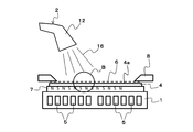
- FIG. 1 is a schematic configuration diagram showing an embodiment of a film forming apparatus according to the present invention.
- This film forming apparatus is for forming a thin film pattern by applying a liquid film forming material to a film forming surface of a substrate through a metal mask and then heating and baking the material. And a heating device 3 and firing means (not shown).
- the stage 1 is provided inside the apparatus body.
- This stage 1 holds, for example, a display panel 4 as a film formation substrate, is formed of a non-metallic material, and is a high frequency (hereinafter referred to as “RF (Radio Frequency)”) that constitutes a heating device 3 described later.
- RF Radio Frequency
- a metal mask 6 made of a magnetic metal material is attracted and displayed by a sheet-like magnet 7 disposed on the back surface opposite to the display surface 4a of the display panel 4. It is closely fixed to the surface 4a.
- the metal mask 6 is provided with a plurality of opening patterns 9 having the same shape and dimensions as the thin film pattern to be formed and formed, for example, with a thickness of 10 ⁇ m to 30 ⁇ m formed of nickel, nickel alloy, invar, or invar alloy
- a frame-shaped metal frame 8 made of invar or invar alloy or the like is joined to the peripheral edge of one surface of the mask sheet.
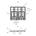
- the metal mask 6 includes a mask layer 10 provided with the plurality of opening patterns 9 and a plurality of openings provided across the opening pattern 9 on one surface of the mask layer 10. And a support layer 11 made of a thin line (hereinafter referred to as “support line 11a”).
- support line 11a a support layer 11 made of a thin line
- the mask layer 10 and the support layer 11 are formed by two-stage electroplating. As a result, even if the width of the partition wall (shadow part) 9a separating the adjacent opening patterns 9 is narrowed, the shape of the opening pattern 9 can be maintained by being held by the plurality of support lines 11a crossing the opening pattern 9. It becomes possible.
- a coating device 2 is provided above the stage 1.
- the coating apparatus 2 uses a liquid film forming material 16 in which, for example, carbon nanotube (CNT), indium tin oxide (ITO) nanoparticles, or metal nanoparticles are dispersed in a solution. It is applied on the display surface 4a and includes a spray nozzle 12 for spraying the film forming material 16.
- the spray nozzle 12 is configured to be movable in a plane parallel to the surface of the stage 1 by a moving mechanism (not shown) as indicated by an arrow in FIG.
- the coating apparatus 2 supplies high-speed air to the tip of the spray nozzle 12, for example, and uses the negative pressure generated at the nozzle tip due to the venturi effect to pass the film forming material 16 from the storage tank through the pipe. It is sucked up and sprayed in the form of a mist with the high-speed air.
- the heating device 3 is provided with the RF induction antenna coil 5 built in the stage 1.
- the heating device 3 is for heating the metal mask 6 that is tightly fixed to the display panel 4 held on the stage 1 at a temperature lower than the heating and baking temperature of the liquid film forming material 16.
- This is a high-frequency induction heating device configured to include an RF power source 13, an RF induction antenna coil 5, and an impedance matching circuit 14.
- the RF power source 13 generates a high frequency of 1.5 kHz to 400 kHz, for example.
- the RF induction antenna coil 5 generates an electromagnetic field around the coil by a high-frequency current flowing through the coil. Due to this induction electromagnetic field, an induced current is generated inside the metal mask 6, and the metal mask 6 self-heats due to Joule heat generated in the metal mask 6.
- the impedance matching circuit 14 is for efficiently transmitting the high-frequency power generated by the RF power source 13 to the RF induction antenna coil 5 and suppresses the reflected wave generated in the transmission line 15 so that the maximum output can be obtained. It is inserted into a transmission line 15 between the power supply 13 and the RF induction antenna coil 5.
- the impedance matching circuit 14 is a general matching device in which a coil L and a capacitor C are combined.
- This baking means is for heating and baking the liquid film-forming material 16 applied to the display panel 4 and is, for example, a resistance heating means.
- the baking means may be built in the stage 1 or may be built in a second stage provided separately from the stage 1.
- the display panel 4 coated with the film forming material 16 may be transferred from the stage 1 to the second stage by a transport mechanism (not shown).
- the metal mask 6 is attracted and fixed to the display surface 4 a of the display panel 4 by being attracted by a sheet-like magnet 7 disposed on the back surface of the display panel 4.
- the metal mask 6 is installed with a distance having a small influence.
- the alignment between the display panel 4 and the metal mask 6 is performed using the alignment reference set in advance for the display panel 4 and the alignment reference set in advance for the metal mask 6.
- the metal mask 6 is lowered and placed on the display panel 4.
- the magnetic force of the magnet 7 disposed on the back surface of the display panel 4 acts on the metal mask 6 and the metal mask 6 is attracted to the display panel 4 side.
- the metal mask 6 is tightly fixed to the display surface 4 a of the display panel 4.
- the display panel 4 to which the metal mask 6 is adhered is placed on the stage 1 in the apparatus main body. Note that the above series of operations may be performed on the stage 1.
- the RF power supply 13 of the heating device 3 is activated, and a high-frequency current is supplied to the RF induction antenna coil 5.
- the capacitance of the capacitor C of the impedance matching circuit 14 is adjusted, and the reflected wave of the transmission line 15 is minimized.
- the heat generated by the metal mask 6 is such that the temperature of the metal mask 6 is lower than the firing temperature (curing temperature: 130 ° C.) of the liquid film forming material 16 to be used, for example, carbon nanotubes. Is set. Since the display panel 4 is a non-metallic material, it is not heated by the high frequency electromagnetic field. Therefore, only the metal mask 6 is mainly heated by induction.
- a liquid film-forming material 16 is sprayed from the spray nozzle 12 toward the display panel 4 as shown in FIG.
- the film forming material 16 is set in advance on the display surface 4a of the display panel 4 corresponding to the opening pattern 9 provided in the mask layer 10 of the metal mask 6, for example, about several hundred nm to several ⁇ m. It is applied to the thickness of The spraying operation of the film forming material 16 by the spray nozzle 12 is performed while reciprocating or zigzag moving the spray nozzle 12 in a plane parallel to the display surface 4 a of the display panel 4.
- the metal mask 6 is attracted by the magnet 7 and is in close contact with the display surface 4 a of the display panel 4, there is a slight gap between the metal mask 6 and the display panel 4. Therefore, when the metal mask 6 is not heated and the flowability of the film forming material 16 to be used is high, the coating liquid of the film forming material 16 is applied to the opening pattern 9 adjacent to the metal mask 6 as shown in FIG. There is a problem that the shape accuracy of the formed thin film pattern is deteriorated by penetrating under the partition wall 9a. In particular, when the width of the partition wall 9a is narrow, there is a possibility that the film forming material 16 applied in the adjacent opening pattern 9 is connected via the bottom of the partition wall 9a.
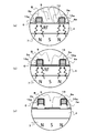
- FIG. 5 is a diagram for explaining the film forming method according to the present invention, and is an enlarged cross-sectional view of a portion B surrounded by a circle in FIG.
- FIG. 5A when the film forming material 16 is sprayed in a state where the metal mask 6 is induction-heated, the film forming material 16 is displayed within the opening pattern 9 of the metal mask 6. It adheres to the display surface 4 a of the panel 4 and to the metal mask 6.
- the film-forming material 16a which is partially cured or has a high viscosity, serves as a barrier, and the film-forming material 16 is prevented from entering under the partition wall 9a of the adjacent opening pattern 9 of the metal mask 6.
- the induction heating of the metal mask 6 is continued until the application of the film forming material 16 is completed as shown in FIG.
- the metal mask 6 is peeled from the display panel 4 as shown in FIG.
- the film forming material 16a attached to the metal mask 6 is partially cured or has a high viscosity, the uncured film forming material 16 and the metal mask attached to the display surface 4a of the display panel 4 are used. 6 is easily separated from the film forming material 16a adhering to 6.
- an application pattern of the film forming material 16 having the shape of the target thin film pattern, in which the shape of the opening pattern 9 of the metal mask 6 is accurately transferred remains on the display surface 4 a of the display panel 4.
- the film forming material 16 adhered to the display panel 4 is heated and fired by a baking means provided inside the apparatus main body. More specifically, when, for example, a resistance heating unit as a baking unit is provided in the stage 1, the resistance heating unit is energized when the metal mask 6 is peeled from the display surface 4a of the display panel 4. Then, the display panel 4 is heated, for example, to a carbon nanotube firing temperature of 130 ° C. Thereby, for example, the carbon nanotubes which are the film forming material 16 attached to the display panel 4 are cured, and a thin film pattern of the carbon nanotubes is formed.
- a baking means provided inside the apparatus main body. More specifically, when, for example, a resistance heating unit as a baking unit is provided in the stage 1, the resistance heating unit is energized when the metal mask 6 is peeled from the display surface 4a of the display panel 4. Then, the display panel 4 is heated, for example, to a carbon nanotube firing temperature of 130 ° C. Thereby, for example, the carbon nanotube
- the baking means is provided in a second stage provided separately from the stage 1, the display panel 4 coated with the film forming material 16 is moved from the stage 1 to the second stage. For example, it is transferred by a transport mechanism (not shown). Then, the display panel 4 is heated in the same manner as described above, and the film forming material 16 is heated and fired to be cured.
- the film forming material 16 is a liquid containing, for example, carbon nanotube (CNT), indium tin oxide (ITO) nanoparticles, or metal nanoparticles
- the formed thin film pattern is a transparent conductive film. . Therefore, according to the manufacturing method of the present invention, the touch panel provided with the transparent electrode on the display panel 4 can also be formed by a simple process.
- the metal mask 6 is formed of a magnetic metal material.
- the present invention is not limited to this, and the metal mask 6 may be formed of a nonmagnetic metal material. In this case, it is not necessary to arrange the magnet 7 on the back surface of the display panel 4.
- the present invention is not limited to this, and the liquid film forming material 16 is applied to the film forming surface of the substrate through the metal mask 6. Then, if it is heat-cured to form a thin film pattern, it can be applied to the formation of circuit wirings, for example.
Landscapes
- Engineering & Computer Science (AREA)
- Manufacturing & Machinery (AREA)
- Chemical & Material Sciences (AREA)
- Microelectronics & Electronic Packaging (AREA)
- Organic Chemistry (AREA)
- Materials Engineering (AREA)
- Mechanical Engineering (AREA)
- Metallurgy (AREA)
- Chemical Kinetics & Catalysis (AREA)
- Life Sciences & Earth Sciences (AREA)
- Wood Science & Technology (AREA)
- Application Of Or Painting With Fluid Materials (AREA)
- Manufacturing Of Printed Wiring (AREA)
- Details Or Accessories Of Spraying Plant Or Apparatus (AREA)
- Coating Apparatus (AREA)
- Chemically Coating (AREA)
- Physical Vapour Deposition (AREA)
Abstract
本発明の成膜方法は、表示パネル(4)の表示面(4a)にメタルマスク(6)を密着させた状態でメタルマスク(6)を加熱しながら、メタルマスク(6)側から表示パネル(4)の表示面(4a)に液体の成膜材料(16)を塗布するステップと、塗布された液体の成膜材料(16)を加熱焼成して薄膜パターンを形成するステップと、を行うものである。
Description
本発明は、基板の成膜面にメタルマスクを介して液体の成膜材料を塗布した後、これを加熱焼成して薄膜パターンを形成する成膜方法に関し、特に薄膜パターンの形成精度を向上しようとする成膜方法及び成膜装置に係るものである。
従来の成膜方法は、透明樹脂基板に対し、金属ナノ粒子含有組成物を所定のパターン状に印刷して金属細線パターンを形成する工程と、前記金属細線パターンに対し中赤外線を照射する工程と、前記金属細線パターンに対しフラッシュ光を照射して加熱焼成を行う工程と、を有するものとなっていた(例えば、特許文献1参照)。
しかし、このような従来の成膜方法においては、印刷用のマスクの少なくとも基板との接触面に撥液処理が施されていても、金属ナノ粒子含有組成物が流動性の高い液体であるときには、マスクのシャドー部と基板との間に上記金属ナノ粒子含有組成物が侵入して正常な薄膜パターンを形成することができない場合があった。
そこで、本発明は、このような問題点に対処し、薄膜パターンの形成精度を向上しようとする成膜方法及び成膜装置を提供することを目的とする。
上記目的を達成するために、本発明による成膜方法は、基板の成膜面にメタルマスクを密着させた状態で前記メタルマスクを加熱しながら、前記メタルマスク側から前記基板の成膜面に液体の成膜材料を塗布するステップと、前記塗布された液体の成膜材料を加熱焼成して薄膜パターンを形成するステップと、を行うものである。
また、本発明による成膜装置は、基板の成膜面にメタルマスクを介して液体の成膜材料を塗布した後、これを加熱焼成して薄膜パターンを形成する成膜装置であって、前記メタルマスクを加熱する加熱装置と、前記加熱装置による前記メタルマスクの加熱中に、前記メタルマスク側から前記基板の成膜面に前記成膜材料を塗布する塗布装置と、を備えたものである。
本発明によれば、メタルマスクを加熱した状態で液体の成膜材料を塗布しているので、メタルマスクに付着した成膜材料は、一部が直ちに硬化又は高粘度となるため、メタルマスクのシャドー部の下に液体の成膜材料が回り込んで付着するのを防止することができる。したがって、メタルマスクの開口パターンの形状を基板上にそのまま転写することができ、薄膜パターンの形成精度を向上することができる。
以下、本発明の実施形態を添付図面に基づいて詳細に説明する。図1は本発明による成膜装置の一実施形態を示す概略構成図である。この成膜装置は、基板の成膜面にメタルマスクを介して液体の成膜材料を塗布した後、これを加熱焼成して薄膜パターンを形成するためのもので、ステージ1と、塗布装置2と、加熱装置3と、図示省略の焼成手段と、を備えて構成されている。
装置本体内部には、ステージ1が設けられている。このステージ1は、被成膜基板としての例えば表示パネル4を保持するもので、非金属材料で形成されており、後述の加熱装置3を構成する高周波(以下「RF(Radio Frequency)」という)誘導アンテナコイル5が内蔵されている。
なお、表示パネル4の表示面4a上には、磁性金属材料からなるメタルマスク6が、表示パネル4の表示面4aとは反対側の裏面に配置されたシート状の磁石7に吸引されて表示面4aに密着固定されている。
上記メタルマスク6は、成膜形成しようとする薄膜パターンと形状寸法の同じ複数の開口パターン9を設けたもので、例えばニッケル、ニッケル合金、インバー又はインバー合金等で形成された厚みが10μm~30μm程度のマスクシートであり、マスクシートの一面の周縁部には、インバー又はインバー合金等から成る枠状の金属フレーム8が接合された構成となっている。
詳細には、上記メタルマスク6は、図2に示すように、上記複数の開口パターン9を設けたマスク層10と、マスク層10の一面に上記開口パターン9を横断して設けられた複数の細線(以下「サポートライン11a」という)からなるサポート層11とを備えた構成を有している。この場合、上記マスク層10とサポート層11とは、2段階電気めっきにより形成される。これにより、隣接する開口パターン9を隔てる隔壁(シャドー部)9aの幅が狭くなっても、上記開口パターン9を横断する複数のサポートライン11aにより保持されて開口パターン9の形状を維持することが可能となる。
上記ステージ1の上方には塗布装置2が設けられている。この塗布装置2は、例えばカーボンナノチューブ(CNT)、インジウムスズ酸化物(indium tin oxide:ITO)のナノ粒子、又は金属ナノ粒子を溶液中に分散させた液体の成膜材料16を表示パネル4の表示面4a上に塗布するもので、上記成膜材料16を噴霧するスプレーノズル12を含むものである。そして、このスプレーノズル12は、図1に矢印で示すように、上記ステージ1の面に平行な面内を図示省略の移動機構によって移動可能に構成されている。
詳細には、上記塗布装置2は、例えばスプレーノズル12の先端部に高速のエアを供給し、ベンチュリ効果によりノズル先端部に発生する負圧を利用して成膜材料16を貯蔵タンクから管を通して吸い上げ、上記高速エアで霧状にして噴射させるものである。
上記ステージ1にRF誘導アンテナコイル5を内蔵させて加熱装置3が設けられている。この加熱装置3は、ステージ1上に保持された表示パネル4に密着固定されているメタルマスク6を、上記液体の成膜材料16の加熱焼成温度よりも低い温度で加熱するためのものであり、RF電源13と、RF誘導アンテナコイル5と、インピーダンスマッチング回路14と、を備えて構成された高周波誘導加熱装置である。
詳細には、RF電源13は、例えば1.5kHz~400kHzの高周波を発生するものである。また、RF誘導アンテナコイル5は、コイルを流れる高周波電流によってコイルの周りに電磁界を発生させるものである。この誘導電磁界により上記メタルマスク6の内部に誘導電流が生じ、それによりメタルマスク6に発生するジュール熱でメタルマスク6が自己発熱する。さらに、インピーダンスマッチング回路14は、RF電源13で発生した高周波電力を効率よくRF誘導アンテナコイル5に伝達するためのもので、伝送路15に生ずる反射波を抑えて最大出力が得られるようにRF電源13とRF誘導アンテナコイル5との間の伝送路15に挿入されている。このインピーダンスマッチング回路14は、コイルLとコンデンサCを組み合わせた一般的な整合器である。
上記装置本体内部には、図示省略の焼成手段が設けられている。この焼成手段は、表示パネル4に塗布された液体の成膜材料16を加熱焼成して硬化させるためのものであり、例えば、抵抗加熱手段等である。この場合、上記焼成手段は、上記ステージ1に内蔵されてもよく、上記ステージ1とは別に設けた第2のステージに内蔵されてもよい。第2のステージに備えた場合には、成膜材料16が塗布された表示パネル4が上記ステージ1から第2のステージに図示省略の搬送機構によって移送されるように構成するとよい。
次に、このように構成された成膜装置の動作及び成膜方法について説明する。
先ず、図1に示すように、表示パネル4の裏面に配置されたシート状の磁石7により吸引されてメタルマスク6が表示パネル4の表示面4aに密着固定される。
先ず、図1に示すように、表示パネル4の裏面に配置されたシート状の磁石7により吸引されてメタルマスク6が表示パネル4の表示面4aに密着固定される。
詳細には、裏面にシート状の磁石7が配置された表示パネル4にマスク層10側を対面させた状態で、表示パネル4の上方に、上記磁石7の磁力の影響が及ばない又は磁力の影響が小さい距離を保ってメタルマスク6が設置される。この状態で、例えば表示パネル4に予め設定されたアライメント基準とメタルマスク6に予め設定されたアライメント基準を使用して表示パネル4とメタルマスク6のアライメントが実施される。そして、両者のアライメントが終了すると、メタルマスク6が下降して表示パネル4上に載置される。このとき、表示パネル4の裏面に配置された磁石7の磁力がメタルマスク6に作用してメタルマスク6が表示パネル4側に吸引される。これにより、メタルマスク6が表示パネル4の表示面4aに密着固定される。
メタルマスク6を密着させた表示パネル4は、装置本体内のステージ1上に載置される。なお、上記一連の動作は、ステージ1上で行ってもよい。
次に、加熱装置3のRF電源13が起動され、高周波の電流がRF誘導アンテナコイル5に供給される。このとき、インピーダンスマッチング回路14のコンデンサCの容量が調節され、伝送路15の反射波が最小にされる。
RF電源13から供給される高周波電流がRF誘導アンテナコイル5を流れることによりコイルの周囲には電磁界が発生する。この電磁界は、メタルマスク6に作用してメタルマスク6の内部に誘導電流を生じさせる。メタルマスク6の内部を誘導電流が流れることにより、メタルマスク6にはジュール熱が発生し、メタルマスク6が自己発熱する。メタルマスク6の発熱量は、RF電源13からRF誘導アンテナコイル5に供給される電力量によって調節することができる。本実施形態においては、メタルマスク6の発熱は、メタルマスク6の温度が、使用する液体の成膜材料16、例えばカーボンナノチューブの焼成温度(硬化温度:130℃)よりも低い温度となるように設定される。なお、表示パネル4は非金属材料であるため上記高周波の電磁界によって加熱されない。したがって、誘導加熱されるのは、主としてメタルマスク6のみである。
メタルマスク6の温度が設定温度に達すると、図3に示すように、スプレーノズル12から液体の成膜材料16が表示パネル4に向けて噴霧される。これにより、メタルマスク6のマスク層10に設けられた開口パターン9内に対応して位置する表示パネル4の表示面4aに、成膜材料16が予め設定された例えば数百nm~数μm程度の厚みに塗布される。このスプレーノズル12による成膜材料16の噴霧動作は、スプレーノズル12を表示パネル4の表示面4aに平行な面内を、例えば往復又はジグザグ移動させながら行われる。
ここで、メタルマスク6が磁石7により吸引されて表示パネル4の表示面4aに密着されてはいるものの、メタルマスク6と表示パネル4との間には僅かな隙間が存在する。したがって、メタルマスク6が加熱されていない場合に、使用する成膜材料16の流動性が高いときには、図4に示すように成膜材料16の塗布液がメタルマスク6の隣接する開口パターン9の隔壁9a下にまで侵入し、形成される薄膜パターンの形状精度が悪くなるという問題がある。特に、隔壁9aの幅が狭いときには、隣接して存在する開口パターン9内に塗布された成膜材料16が隔壁9aの下を介して繋がってしまうおそれがある。
そこで、本発明においては、メタルマスク6を加熱した状態で成膜材料16を塗布することにより、上記問題に対処している。これについて、以下に詳細に説明する。
図5は、本発明による成膜方法を説明する図であり、図3の円で囲ったBの部分を拡大して示す断面図である。
先ず、図5(a)に示すように、メタルマスク6が誘導加熱された状態で成膜材料16が噴霧されると、成膜材料16は、メタルマスク6の開口パターン9内に位置する表示パネル4の表示面4a上及びメタルマスク6に付着する。
図5は、本発明による成膜方法を説明する図であり、図3の円で囲ったBの部分を拡大して示す断面図である。
先ず、図5(a)に示すように、メタルマスク6が誘導加熱された状態で成膜材料16が噴霧されると、成膜材料16は、メタルマスク6の開口パターン9内に位置する表示パネル4の表示面4a上及びメタルマスク6に付着する。
この場合、メタルマスク6が加熱されているため、図5(a)に斜線を付して示すように、メタルマスク6に付着した成膜材料16aは、一部が硬化する又は高粘度となる。したがって、この一部が硬化した又は高粘度となった成膜材料16aが障壁となって、メタルマスク6の隣接する開口パターン9の隔壁9a下への成膜材料16の侵入が阻止される。
メタルマスク6の誘導加熱は、図5(b)に示すように、成膜材料16の塗布が終了するまで続けられる。成膜材料16の塗布が終了すると、同図(c)に示すように、メタルマスク6が表示パネル4から剥離される。ことのき、メタルマスク6に付着した成膜材料16aは、一部が硬化し又は高粘度となっているため、表示パネル4の表示面4aに付着した未硬化の成膜材料16とメタルマスク6に付着した成膜材料16aとは、容易に切り離される。これにより、表示パネル4の表示面4aには、メタルマスク6の開口パターン9の形状を正確に転写した、目的とする薄膜パターンの形状を有する成膜材料16の塗布パターンが残ることになる。
表示パネル4に付着した成膜材料16は、装置本体内部に設けられた焼成手段によって加熱焼成される。詳細には、焼成手段としての例えば抵抗加熱手段が上記ステージ1に内蔵して設けられている場合には、表示パネル4の表示面4aからメタルマスク6が剥離されると、抵抗加熱手段に通電されて表示パネル4が例えばカーボンナノチューブの焼成温度130℃に加熱される。これにより、表示パネル4に付着した成膜材料16である例えばカーボンナノチューブが硬化し、カーボンナノチューブの薄膜パターンが形成される。
又は、焼成手段が上記ステージ1とは別に設けた第2のステージに内蔵して備えられている場合には、成膜材料16が塗布された表示パネル4が上記ステージ1から第2のステージに、例えば図示省略の搬送機構によって移送される。そして、上記と同様にして表示パネル4が加熱され、成膜材料16が加熱焼成されて硬化される。
この場合、成膜材料16が例えばカーボンナノチューブ(CNT)、インジウムスズ酸化物(ITO)のナノ粒子、又は金属ナノ粒子を含有する液体であるときには、形成される薄膜パターンは、透明導電膜となる。したがって、本発明の製造方法によれば、表示パネル4に透明電極を備えたタッチパネルも簡単な工程で形成することができる。
なお、上記実施形態においては、メタルマスク6が磁性金属材料で形成されている場合について説明したが、本発明はこれに限られず、メタルマスク6は非磁性金属材料で形成されてもよい。この場合、表示パネル4の裏面に磁石7を配置する必要はない。
また、上記実施形態においては、タッチパネル用の透明電極を形成する場合について説明したが、本発明はこれに限られず、基板の成膜面にメタルマスク6を介して液体の成膜材料16を塗布した後、これを加熱硬化させて薄膜パターンを形成するものであれば、例えば回路の配線等の形成にも適用することができる。
1…ステージ
2…塗布装置
3…加熱装置
4…表示パネル(基板)
4a…表示面(成膜面)
5…高周波誘導アンテナコイル
6…メタルマスク
7…磁石
9…開口パターン
10…マスク層
11…サポート層
11a…サポートライン(細線)
16…成膜材料
2…塗布装置
3…加熱装置
4…表示パネル(基板)
4a…表示面(成膜面)
5…高周波誘導アンテナコイル
6…メタルマスク
7…磁石
9…開口パターン
10…マスク層
11…サポート層
11a…サポートライン(細線)
16…成膜材料
Claims (12)
- 基板の成膜面にメタルマスクを密着させた状態で前記メタルマスクを加熱しながら、前記メタルマスク側から前記基板の成膜面に液体の成膜材料を塗布するステップと、
前記塗布された液体の成膜材料を加熱焼成して薄膜パターンを形成するステップと、
を行うことを特徴とする成膜方法。 - 前記メタルマスクの加熱温度は、前記液体の成膜材料の加熱焼成温度よりも低く設定されていることを特徴とする請求項1記載の成膜方法。
- 前記メタルマスクの加熱は、高周波誘導加熱によるものであることを特徴とする請求項1又は2記載の成膜方法。
- 前記メタルマスクは、前記基板の成膜面とは反対側に配置された磁石により吸引されて前記成膜面に密着され得るように磁性金属材料で形成されていることを特徴とする請求項1又は2記載の成膜方法。
- 前記メタルマスクは、前記薄膜パターンと形状寸法の同じ開口パターンを設けたマスク層と、前記開口パターンを横断して前記マスク層の一面に設けられた複数の細線を有するサポート層と、を備え、前記マスク層を前記基板の成膜面に密着させて使用されることを特徴とする請求項1又は2記載の成膜方法。
- 前記液体の成膜材料は、カーボンナノチューブ、インジウムスズ酸化物のナノ粒子、又は金属ナノ粒子を溶液中に分散させたものであることを特徴とする請求項1又は2記載の成膜方法。
- 基板の成膜面にメタルマスクを介して液体の成膜材料を塗布した後、これを加熱焼成して薄膜パターンを形成する成膜装置であって、
前記メタルマスクを加熱する加熱装置と、
前記加熱装置による前記メタルマスクの加熱中に、前記メタルマスク側から前記基板の成膜面に前記成膜材料を塗布する塗布装置と、
を備えたことを特徴とする成膜装置。 - 前記加熱装置は、高周波誘導加熱装置であることを特徴とする請求項7記載の成膜装置。
- 前記高周波誘導加熱装置は、前記基板を保持するステージに内蔵された高周波誘導アンテナコイルを含むことを特徴とする請求項8記載の成膜装置。
- 前記メタルマスクは、前記基板の前記成膜面とは反対側に配置された磁石により吸引されて前記成膜面に密着され得るように磁性金属材料で形成されていることを特徴とする請求項7~9のいずれか1項に記載の成膜装置。
- 前記メタルマスクは、前記薄膜パターンと形状寸法の同じ開口パターンを設けたマスク層と、前記開口パターンを横断して前記マスク層の一面に設けられた複数の細線を有するサポート層と、を備え、前記マスク層を前記基板の成膜面に密着させて使用されることを特徴とする請求項7~9のいずれか1項に記載の成膜装置。
- 前記液体の成膜材料は、カーボンナノチューブ、インジウムスズ酸化物のナノ粒子、又は金属ナノ粒子を溶液中に分散させたものであることを特徴とする請求項7~9のいずれか1項に記載の成膜装置。
Priority Applications (3)
| Application Number | Priority Date | Filing Date | Title |
|---|---|---|---|
| KR1020167032627A KR20170032223A (ko) | 2014-07-14 | 2015-07-03 | 성막 방법 및 성막 장치 |
| CN201580038458.9A CN106536066A (zh) | 2014-07-14 | 2015-07-03 | 成膜方法和成膜装置 |
| US15/380,957 US20170099737A1 (en) | 2014-07-14 | 2016-12-15 | Deposition method and apparatus |
Applications Claiming Priority (2)
| Application Number | Priority Date | Filing Date | Title |
|---|---|---|---|
| JP2014143972A JP6446736B2 (ja) | 2014-07-14 | 2014-07-14 | 成膜方法及び成膜装置 |
| JP2014-143972 | 2014-07-14 |
Related Child Applications (1)
| Application Number | Title | Priority Date | Filing Date |
|---|---|---|---|
| US15/380,957 Continuation US20170099737A1 (en) | 2014-07-14 | 2016-12-15 | Deposition method and apparatus |
Publications (1)
| Publication Number | Publication Date |
|---|---|
| WO2016009857A1 true WO2016009857A1 (ja) | 2016-01-21 |
Family
ID=55078355
Family Applications (1)
| Application Number | Title | Priority Date | Filing Date |
|---|---|---|---|
| PCT/JP2015/069287 Ceased WO2016009857A1 (ja) | 2014-07-14 | 2015-07-03 | 成膜方法及び成膜装置 |
Country Status (6)
| Country | Link |
|---|---|
| US (1) | US20170099737A1 (ja) |
| JP (1) | JP6446736B2 (ja) |
| KR (1) | KR20170032223A (ja) |
| CN (1) | CN106536066A (ja) |
| TW (1) | TW201605719A (ja) |
| WO (1) | WO2016009857A1 (ja) |
Families Citing this family (5)
| Publication number | Priority date | Publication date | Assignee | Title |
|---|---|---|---|---|
| JP6341434B2 (ja) * | 2016-03-29 | 2018-06-13 | 株式会社ブイ・テクノロジー | 成膜マスク、その製造方法及び成膜マスクのリペア方法 |
| CN117505141A (zh) | 2019-05-16 | 2024-02-06 | 蜻蜓能源公司 | 用于电化学电池的干粉涂层的系统和方法 |
| CN115055403B (zh) * | 2022-06-20 | 2023-09-26 | 安徽九鲤智能设备有限公司 | 一种具备消毒功能的滑块分拣机的滑块机构 |
| CN115672602A (zh) * | 2022-09-21 | 2023-02-03 | 中芯热成科技(北京)有限责任公司 | 喷涂装置、方法、胶体量子点薄膜、器件及其制备方法 |
| KR102882307B1 (ko) * | 2022-10-21 | 2025-11-06 | 성균관대학교산학협력단 | 생체모방 자성 금 나노 성게 입자를 이용한 고감도 중금속 이온 검출 센서 |
Citations (12)
| Publication number | Priority date | Publication date | Assignee | Title |
|---|---|---|---|---|
| JPH09320758A (ja) * | 1996-06-03 | 1997-12-12 | Fuji Electric Co Ltd | 真空成膜用マスク |
| JPH10330910A (ja) * | 1997-06-04 | 1998-12-15 | Toray Ind Inc | シャドーマスクおよびその製造方法 |
| JP2001254169A (ja) * | 2000-03-13 | 2001-09-18 | Optonix Seimitsu:Kk | 蒸着用金属マスクおよび蒸着用金属マスク製造方法 |
| JP2005191416A (ja) * | 2003-12-26 | 2005-07-14 | Ricoh Co Ltd | 電子素子の製造方法 |
| JP2006218460A (ja) * | 2005-02-14 | 2006-08-24 | Pioneer Electronic Corp | 塗布物被塗布材の製造方法および製造装置 |
| JP2006310693A (ja) * | 2005-05-02 | 2006-11-09 | Sony Corp | 接着剤塗布装置および接着剤塗布方法 |
| JP2007175619A (ja) * | 2005-12-28 | 2007-07-12 | Mitsuboshi Belting Ltd | 金属薄膜の製造方法 |
| WO2007088945A1 (ja) * | 2006-02-02 | 2007-08-09 | Pioneer Corporation | 成膜用マスク、表示装置の製造方法、および表示装置 |
| JP2009056402A (ja) * | 2007-08-31 | 2009-03-19 | Sharp Corp | パターン膜の製造方法、パターン膜、有機薄膜トランジスタ、有機発光デバイス、溶液滴下装置、パターン膜製造用マスク |
| JP2009289474A (ja) * | 2008-05-27 | 2009-12-10 | Casio Comput Co Ltd | 発光装置及び発光装置の製造方法 |
| JP2011502034A (ja) * | 2007-10-12 | 2011-01-20 | トップ・ナノシス・インコーポレーテッド | スプレーコーティングを用いたカーボンナノチューブ導電膜およびその製造方法 |
| JP2013193407A (ja) * | 2012-03-22 | 2013-09-30 | Nec Corp | スクリーン印刷装置及びスクリーン印刷方法 |
Family Cites Families (3)
| Publication number | Priority date | Publication date | Assignee | Title |
|---|---|---|---|---|
| JPH07236842A (ja) * | 1994-02-28 | 1995-09-12 | Kanto Auto Works Ltd | 塗装用マスキング具及びその使用方法 |
| US6230619B1 (en) * | 1996-05-17 | 2001-05-15 | Matsushita Electric Industrial Co., Ltd. | Printing method and printing apparatus |
| JP5983173B2 (ja) | 2012-08-14 | 2016-08-31 | コニカミノルタ株式会社 | 透明電極の製造方法および有機電子素子の製造方法 |
-
2014
- 2014-07-14 JP JP2014143972A patent/JP6446736B2/ja not_active Expired - Fee Related
-
2015
- 2015-07-03 WO PCT/JP2015/069287 patent/WO2016009857A1/ja not_active Ceased
- 2015-07-03 CN CN201580038458.9A patent/CN106536066A/zh active Pending
- 2015-07-03 KR KR1020167032627A patent/KR20170032223A/ko not_active Withdrawn
- 2015-07-13 TW TW104122476A patent/TW201605719A/zh unknown
-
2016
- 2016-12-15 US US15/380,957 patent/US20170099737A1/en not_active Abandoned
Patent Citations (12)
| Publication number | Priority date | Publication date | Assignee | Title |
|---|---|---|---|---|
| JPH09320758A (ja) * | 1996-06-03 | 1997-12-12 | Fuji Electric Co Ltd | 真空成膜用マスク |
| JPH10330910A (ja) * | 1997-06-04 | 1998-12-15 | Toray Ind Inc | シャドーマスクおよびその製造方法 |
| JP2001254169A (ja) * | 2000-03-13 | 2001-09-18 | Optonix Seimitsu:Kk | 蒸着用金属マスクおよび蒸着用金属マスク製造方法 |
| JP2005191416A (ja) * | 2003-12-26 | 2005-07-14 | Ricoh Co Ltd | 電子素子の製造方法 |
| JP2006218460A (ja) * | 2005-02-14 | 2006-08-24 | Pioneer Electronic Corp | 塗布物被塗布材の製造方法および製造装置 |
| JP2006310693A (ja) * | 2005-05-02 | 2006-11-09 | Sony Corp | 接着剤塗布装置および接着剤塗布方法 |
| JP2007175619A (ja) * | 2005-12-28 | 2007-07-12 | Mitsuboshi Belting Ltd | 金属薄膜の製造方法 |
| WO2007088945A1 (ja) * | 2006-02-02 | 2007-08-09 | Pioneer Corporation | 成膜用マスク、表示装置の製造方法、および表示装置 |
| JP2009056402A (ja) * | 2007-08-31 | 2009-03-19 | Sharp Corp | パターン膜の製造方法、パターン膜、有機薄膜トランジスタ、有機発光デバイス、溶液滴下装置、パターン膜製造用マスク |
| JP2011502034A (ja) * | 2007-10-12 | 2011-01-20 | トップ・ナノシス・インコーポレーテッド | スプレーコーティングを用いたカーボンナノチューブ導電膜およびその製造方法 |
| JP2009289474A (ja) * | 2008-05-27 | 2009-12-10 | Casio Comput Co Ltd | 発光装置及び発光装置の製造方法 |
| JP2013193407A (ja) * | 2012-03-22 | 2013-09-30 | Nec Corp | スクリーン印刷装置及びスクリーン印刷方法 |
Also Published As
| Publication number | Publication date |
|---|---|
| JP6446736B2 (ja) | 2019-01-09 |
| TW201605719A (zh) | 2016-02-16 |
| KR20170032223A (ko) | 2017-03-22 |
| JP2016019937A (ja) | 2016-02-04 |
| US20170099737A1 (en) | 2017-04-06 |
| CN106536066A (zh) | 2017-03-22 |
Similar Documents
| Publication | Publication Date | Title |
|---|---|---|
| JP6446736B2 (ja) | 成膜方法及び成膜装置 | |
| JP5341966B2 (ja) | パターン転写方法及びパターン転写装置、これを適用したフレキシブルディスプレイパネル、フレキシブル太陽電池、電子本、薄膜トランジスター、電磁波遮蔽シート、フレキシブル印刷回路基板 | |
| CN105154830B (zh) | 一种固定方法和蒸镀方法 | |
| CN105121692B (zh) | 成膜掩模 | |
| CN109478580B (zh) | 微发光二极管转移方法、制造方法及器件 | |
| US20110209749A1 (en) | Pattern transfer method and apparatus, flexible display panel, flexible solar cell, electronic book, thin film transistor, electromagnetic-shielding sheet, and flexible printed circuit board applying thereof | |
| JP2013209710A (ja) | 蒸着マスク、蒸着マスクの製造方法及び有機el表示装置の製造方法 | |
| US20110203937A1 (en) | Additive manufacturing processes | |
| CN106605294B (zh) | 元件制造方法及转印基板 | |
| Liu et al. | Theoretical and experimental studies of electrostatic focusing for electrohydrodynamic jet printing | |
| CN104766931B (zh) | 一种显示基板的制造方法、显示基板和显示装置 | |
| WO2015163127A1 (ja) | 成膜マスク、成膜マスクの製造方法及びタッチパネルの製造方法 | |
| KR20120042022A (ko) | 패턴 제조 방법 및 패턴 전사 장치, 이를 적용한 플렉서블 디스플레이 패널, 플렉서블 태양전지, 전자책, 박막 트랜지스터, 전자파 차폐시트, 플렉서블 인쇄회로기판 | |
| US9955585B2 (en) | Conductive pattern production device | |
| CN108779549A (zh) | 蒸镀遮罩、蒸镀遮罩的制造方法及有机半导体元件的制造方法 | |
| CN109216926B (zh) | 辐射装置 | |
| KR101164061B1 (ko) | 패턴 제조 방법 및 패턴 전사 장치, 이를 적용한 플렉서블 디스플레이 패널, 플렉서블 태양전지, 전자책, 박막 트랜지스터, 전자파 차폐시트, 플렉서블 인쇄회로기판 | |
| WO2016065799A1 (zh) | 掩模板及其制造方法、利用掩模板构图的方法 | |
| CN105632652A (zh) | 一种高性能精细化透明导电电极的制备方法 | |
| JPWO2020012626A1 (ja) | 回路形成方法、および回路形成装置 | |
| TWI609610B (zh) | 顯示器修復裝置及方法 | |
| TW201230436A (en) | Organic EL elements for lighting and method for manufacturing same | |
| JP2013077541A (ja) | 薄膜パターン形成方法及び有機el表示装置の製造方法 | |
| WO2018010229A1 (zh) | 有机薄膜晶体管制备方法及设备 | |
| KR102195136B1 (ko) | 플라즈마 처리 장치 및 방법 |
Legal Events
| Date | Code | Title | Description |
|---|---|---|---|
| 121 | Ep: the epo has been informed by wipo that ep was designated in this application |
Ref document number: 15821950 Country of ref document: EP Kind code of ref document: A1 |
|
| ENP | Entry into the national phase |
Ref document number: 20167032627 Country of ref document: KR Kind code of ref document: A |
|
| NENP | Non-entry into the national phase |
Ref country code: DE |
|
| 122 | Ep: pct application non-entry in european phase |
Ref document number: 15821950 Country of ref document: EP Kind code of ref document: A1 |