WO2016009826A1 - 光学素子 - Google Patents
光学素子 Download PDFInfo
- Publication number
- WO2016009826A1 WO2016009826A1 PCT/JP2015/068814 JP2015068814W WO2016009826A1 WO 2016009826 A1 WO2016009826 A1 WO 2016009826A1 JP 2015068814 W JP2015068814 W JP 2015068814W WO 2016009826 A1 WO2016009826 A1 WO 2016009826A1
- Authority
- WO
- WIPO (PCT)
- Prior art keywords
- optical element
- depth
- recess
- recesses
- steps
- Prior art date
Links
Images


Classifications
-
- G—PHYSICS
- G02—OPTICS
- G02B—OPTICAL ELEMENTS, SYSTEMS OR APPARATUS
- G02B1/00—Optical elements characterised by the material of which they are made; Optical coatings for optical elements
- G02B1/10—Optical coatings produced by application to, or surface treatment of, optical elements
- G02B1/11—Anti-reflection coatings
- G02B1/111—Anti-reflection coatings using layers comprising organic materials
-
- G—PHYSICS
- G02—OPTICS
- G02B—OPTICAL ELEMENTS, SYSTEMS OR APPARATUS
- G02B1/00—Optical elements characterised by the material of which they are made; Optical coatings for optical elements
- G02B1/10—Optical coatings produced by application to, or surface treatment of, optical elements
- G02B1/11—Anti-reflection coatings
- G02B1/118—Anti-reflection coatings having sub-optical wavelength surface structures designed to provide an enhanced transmittance, e.g. moth-eye structures
-
- G—PHYSICS
- G02—OPTICS
- G02B—OPTICAL ELEMENTS, SYSTEMS OR APPARATUS
- G02B27/00—Optical systems or apparatus not provided for by any of the groups G02B1/00 - G02B26/00, G02B30/00
- G02B27/0018—Optical systems or apparatus not provided for by any of the groups G02B1/00 - G02B26/00, G02B30/00 with means for preventing ghost images
-
- G—PHYSICS
- G02—OPTICS
- G02B—OPTICAL ELEMENTS, SYSTEMS OR APPARATUS
- G02B5/00—Optical elements other than lenses
- G02B5/02—Diffusing elements; Afocal elements
- G02B5/0205—Diffusing elements; Afocal elements characterised by the diffusing properties
- G02B5/021—Diffusing elements; Afocal elements characterised by the diffusing properties the diffusion taking place at the element's surface, e.g. by means of surface roughening or microprismatic structures
- G02B5/0231—Diffusing elements; Afocal elements characterised by the diffusing properties the diffusion taking place at the element's surface, e.g. by means of surface roughening or microprismatic structures the surface having microprismatic or micropyramidal shape
Definitions
- the present invention relates to an optical element.
- This application claims priority based on Japanese Patent Application No. 2014-144899 filed in Japan on July 15, 2014 and Japanese Patent Application No. 2015-078526 filed in Japan on April 7, 2015 And the contents thereof are incorporated herein.
- a film-like antireflection structure for improving visibility is often provided on the surface of a display such as a personal computer.
- This method uses the principle of a so-called moth eye structure.
- the moth-eye structure is intended to prevent reflection by continuously changing the refractive index with respect to incident light in the thickness direction of the substrate, thereby eliminating the discontinuous interface of the refractive index.
- the antireflection structure is not limited to a minute convex portion, and may be a minute concave portion. It is preferable that the ratio of the height or depth (hereinafter referred to as aspect ratio) to the width of the structure of the fine convex portion or concave portion is large. This is because when the aspect ratio is large, the refractive index change becomes more gradual, and high antireflection performance can be obtained. On the other hand, when the aspect ratio is increased, the stability of the antireflection structure having a convex or concave structure is lost, and it is difficult to maintain the shape of the structure.
- Patent Document 1 describes that the antireflection performance of an optical element is improved by providing two or more steps on a convex portion or a concave portion.
- a discontinuous interface is generated in the interface in which the refractive index due to the moth-eye structure continuously changes. This discontinuous interface reflects a portion of the incident light.
- Patent Document 1 proposes that reflected light is reduced by causing the lights reflected at the discontinuous interface to interfere with each other.
- Patent Document 1 has insufficient antireflection performance.
- it is necessary to increase the frequency with which reflected light interferes, and it is necessary to form more steps in the convex portion or the concave portion.
- Such a convex portion or concave portion having a large number of steps needs to be manufactured through a complicated process and is difficult to manufacture.
- the present invention has been made in view of the above circumstances, and an object thereof is to provide an optical element that has high antireflection performance and is easy to manufacture.
- the present inventors have conducted extensive research focusing on the step width and step position of the recess formed in the antireflection layer. As a result, it has been found that the width and position of the step of the recess may be provided within a predetermined range.
- the present invention includes the following inventions.
- An antireflection layer having a plurality of minute recesses having a most frequent pitch equal to or less than the wavelength of light under the environment of use on a substrate, wherein 80% or more of the recesses include one or more steps.
- An optical element having the following condition: (where d is the diameter of the concave portion, h is the depth of the concave portion, and w s is a step of each step at an arbitrary cutting plane) The sum of the widths, z s is the average depth of each of these steps.)
- An antireflective layer having a plurality of minute recesses having a most frequent pitch equal to or less than the wavelength of light in a use environment is provided on a substrate, and 80% or more of the recesses include two or less steps.
- An antireflection layer having a plurality of minute recesses having a most frequent pitch equal to or less than the wavelength of light under the usage environment is provided on a substrate, and 80% or more of the recesses have one step.
- the optical element of the present invention has a high antireflection performance because it has an antireflection layer in which minute recesses are formed on a substrate, and the recesses have steps at predetermined widths and predetermined positions. Since the steps are provided at a predetermined width and a predetermined position, the number of steps can be reduced, and manufacturing can be performed more easily.
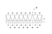
- FIG. 1 is a cross-sectional view schematically showing an optical element of the present invention.
- FIG. 2 is a perspective view schematically showing the optical element of the present invention
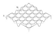
- FIG. 3 is a plan view schematically showing the optical element of the present invention.
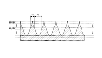
- the optical element 10 includes an antireflection layer 2 on a substrate 1 in which a plurality of minute concave portions c1 to cn having a most frequent pitch P equal to or less than the wavelength of light under the usage environment is formed.
- the optical element 10 may have a flat portion f between the concave portions c1 to cn.
- t1 to tn are the center points of the recesses c1 to cn.
- a plurality of contour lines are drawn for each recess in parallel with the reference plane every 20 nm, and the center of gravity (point determined by the x coordinate and y coordinate) of each contour line is obtained.
- the average position of these centroid points is the center point of the recess.
- m1 to mn are the midpoints of adjacent center points obtained by AFM.
- the flat surface f is based on the AFM measurement result, and the inclination of the straight line connecting the position coordinates at the midpoint in the area and the position coordinates of any point in the area with respect to the reference plane of the AFM is ⁇ 10 ° or less. It is an area.
- the reference plane was a plane parallel to the substrate surface in the measurement region, and was a plane passing through a reference point described later.
- the most frequent pitch P is a distance between adjacent recesses, and can be specifically obtained as follows. First, an AFM image is obtained for a region selected at random on the substrate 1 and having a square region whose side is 30 to 40 times the most frequent pitch P. For example, when the most frequent pitch is about 300 nm, an image of an area of 9 ⁇ m ⁇ 9 ⁇ m to 12 ⁇ m ⁇ 12 ⁇ m is obtained. Then, this image is waveform-separated by Fourier transform to obtain an FFT image (fast Fourier transform image). Next, the distance from the zero-order peak to the primary peak in the profile of the FFT image is obtained. The reciprocal of the distance thus obtained is the most frequent pitch P in this region.
- each region is preferably selected at least 1 mm apart, more preferably 5 mm to 1 cm apart.
- the recesses c1 to cn may be divided into a plurality of areas C 1 to C n as shown in FIG.
- Each of the areas C 1 to C n is an area in which the center points of the seven adjacent recesses are continuously aligned in a positional relationship where the six vertexes of the regular hexagon and the intersections of the diagonal lines.
- the position of the center point of each recess is indicated by a circle u centered on the center point.
- the positional relationship in which the center points of the adjacent seven concave portions are the intersections of the six vertexes of the regular hexagon and the diagonal line specifically refers to a relationship satisfying the following conditions.
- a line segment L1 having a length equal to the most frequent pitch P is drawn in the direction from one central point t1 to the adjacent central point t2.
- line segments L2 to L6 having a length equal to the most frequent pitch P are drawn from the center point t1 in directions of 60 °, 120 °, 180 °, 240 °, and 300 ° with respect to the line segment L1. If the six center points adjacent to the center point t1 are within 15% of the most frequent pitch P from the end points of the line segments L1 to L6 on the side opposite to the center point t1, these seven center points are It is in a positional relationship that is the intersection of six vertices of a regular hexagon and a diagonal line.
- the mode Q of each area C 1 to C n (the mode value of each area) is preferably in the following range.
- the modal area Q is in the AFM image measurement range of 10 [mu] m ⁇ 10 [mu] m, is preferably 0.026 ⁇ m 2 ⁇ 6.5 ⁇ m 2.
- the modal area Q is in the AFM image measurement range of 10 [mu] m ⁇ 10 [mu] m, is preferably 0.65 ⁇ m 2 ⁇ 26 ⁇ m 2.
- most frequent pitch P is not less than 1 [mu] m
- most frequent area Q is in the AFM image measuring range of 50 [mu] m ⁇ 50 [mu] m, is preferably 2.6 ⁇ m 2 ⁇ 650 ⁇ m 2. If the most frequent area Q is within a preferable range, it is easy to prevent the problem that the viewing angle dependency of the antireflection performance is increased.
- the areas C 1 to C n have random areas, shapes, and lattice orientations. Specifically, the degree of randomness of the area preferably satisfies the following conditions. First, an ellipse having the maximum area that circumscribes the border of one area is drawn, and the ellipse is expressed by the following equation (7). When the most frequent pitch P is less than 500 nm, the standard deviation of ⁇ ab in the 10 ⁇ m ⁇ 10 ⁇ m AFM image measurement range is preferably 0.08 ⁇ m 2 or more.
- the standard deviation of ⁇ ab in the AFM image measurement range of 10 ⁇ m ⁇ 10 ⁇ m is preferably 1.95 ⁇ m 2 or more.
- the standard deviation of ⁇ ab in the AFM image measurement range of 50 ⁇ m ⁇ 50 ⁇ m is preferably 8.58 ⁇ m 2 or more. If the standard deviation of ⁇ ab is within a preferable range, the effect of averaging the reflected light is excellent, and the problem that the viewing angle dependency of the antireflection performance is high can be easily prevented.
- the degree of randomness of the shapes of the areas C 1 to C n is preferably such that the ratio of a to b and the standard deviation of a / b in the formula (7) are 0.1 or more.
- the randomness of the lattice orientation of each area C 1 to C n preferably satisfies the following conditions. First, a straight line K0 connecting the center points of any two adjacent recesses in any area (I) is drawn. Next, one area (II) adjacent to the area (I) is selected, and six straight lines K1 connecting an arbitrary recess in the area (II) and the center points of the six recesses adjacent to the recess. Draw ⁇ K6.
- the straight lines K1 to K6 are all at an angle different from the straight line K0 by 3 degrees or more, it is defined that the lattice orientations of the area (I) and the area (II) are different.
- the areas adjacent to the area (I) there are preferably two or more areas having a lattice orientation different from the lattice orientation of the area (I), preferably 3 or more, and more preferably 5 or more.
- the recesses c1 to cn are polycrystalline structures whose lattice orientations are aligned within each of the areas C 1 to C n but are not aligned macroscopically.
- the randomness of the macroscopic lattice orientation can be evaluated by the ratio between the maximum value and the minimum value of the FFT (Fast Fourier Transform) fundamental wave.
- the ratio between the maximum value and the minimum value of the FFT fundamental wave is obtained by acquiring an AFM image, obtaining a two-dimensional Fourier transform image thereof, and drawing a circle away from the origin by the wave number of the fundamental wave.
- the point having the largest amplitude and the point having the smallest amplitude are extracted and obtained as a ratio of the amplitudes.
- the method for acquiring the AFM image at this time is the same as the method for acquiring the AFM image when obtaining the most frequent pitch P.
- the ratio of the maximum value and the minimum value of the FFT fundamental wave is large, the lattice orientation of the recesses is uniform, and when the recess is regarded as a two-dimensional crystal, it can be said that the structure has high single crystallinity.
- the ratio between the maximum value and the minimum value of the FFT fundamental wave is small, the lattice orientations of the recesses are not aligned, and when the recess is regarded as a two-dimensional crystal, it can be said that it has a polycrystalline structure.
- the concave portions c1 to cn have a ratio between the maximum value and the minimum value of the FFT fundamental wave in the preferable range, the reflected light reflected by the step surface is not reflected in a specific in-plane direction, and is reflected evenly. Is done. Therefore, the in-plane reflection intensity does not vary depending on the viewing angle. In other words, antireflection performance with low viewing angle dependency can be obtained.
- More than 80% of the recesses c1 to cn have one or more steps and satisfy the following conditions.
- d is the diameter of the recess
- h is the depth of the recess
- w s is the sum of the widths of each step in an arbitrary cut plane
- z s is the average value of the depth of each step. is there.
- the width and depth of the step are within the above range, high antireflection performance is exhibited for an optical element having no step. If the step width and depth are within the above ranges, high antireflection performance can be obtained even with three or less steps, and a desired optical element can be more easily produced.
- the ratio of the recessed part which has a step is judged as follows. From the AFM image, a cross section as shown in FIG. 1 is obtained along a line having a length of 5 ⁇ m in an arbitrary direction and position.
- the cross section as shown in FIG. 1 may be obtained as a microscopic image obtained by observing a cross section of a cut sample obtained by cutting the optical element with a microscope.
- the cross section measured with the AFM image is given priority. This is because the cross section measured with the AFM image is easier to obtain the measurement surface of the cut surface passing through the deepest part of each recess, and the relationship between the step width and depth is easier to confirm.
- the cross section is an arbitrary plane perpendicular to the arrangement plane in which the concave portions are arranged. When the recesses are regularly arranged, it is preferable that the cutting direction for obtaining the cross section is a direction along the arrangement direction of the recesses.
- the shape (including depth and step position) of the concave portion may be confirmed by confirming the shape of the convex portion of the transfer product that is reversely transferred using the optical element as a mold.
- the cross section of the transferred product may be measured with an AFM image, or the cut surface may be directly observed with a microscope. From the viewpoint of obtaining a cut surface passing through the top of the transferred product, the cut surface is preferably measured by an AFM image.
- An arbitrary portion including 30 to 40 or more recesses in the cross section is extracted, and the ratio of the recesses having steps is measured for each recess included therein.
- the diameter d can be obtained as the maximum diameter in the recess when a cross section perpendicular to the array surface of the recess is observed.
- Depth h is the height of the deepest point and the highest part of the recess when the cross section perpendicular to the arrangement surface of the recesses is observed (the portion farthest from the deepest point on the cut surface: hereinafter referred to as “reference point”). Obtained by calculating the difference.
- the step, step width, and step depth are defined as follows.
- the concave portions c1 to cn may have fine irregularities that are negligible in terms of function and effect in the shape of the envelope surface, and such fine irregularities are set after being ignored. Specifically, a change of 3% or less of the depth h of the recesses c1 to cn is ignored with respect to the fitting curve of the recess.
- B Draw a tangent line at each inflection point.
- C The point closest to the intersection of tangents is taken as the changing point.
- D Connect each change point with a straight line.
- the inflection point means a point at which a curve on a plane changes from convex upward to convex downward or convex downward to convex upward.
- Impossible points are also inflection points in a broad sense.
- the two inflection points are a point that is close to infinity from the reference point side with respect to the point at which the curve is bent, and a point that is close to infinity from the deepest point side with respect to the point at which the curve is bent.
- FIG. 4A The method of obtaining this inflection point in a broad sense is specifically shown using FIG. 4A.
- the reference point when checking in order from the reference point of the recess, the reference point first becomes the first inflection point.
- the points where the direction of the unevenness of the curve changes become the second inflection point and the third inflection point in order from the point close to the reference point.
- the points at which the curve bends are the fourth and fifth inflection points.
- the points where the direction of the unevenness of the curve changes become the sixth inflection point and the seventh inflection point in order from the point close to the reference point.
- the inflection point is set to two points: a point that is close to infinity from the reference point side with respect to the point where the curve bends, and a point that is close to infinity from the deepest point side with respect to the point where the curve is bent.
- the tangent lines drawn from these two points are a straight line having an inclination just before bending from the reference point side to the deepest point side and a straight line having an immediately following inclination, so that two tangent lines can be drawn as shown in FIG. 4B.
- Other inflection points can be mathematically tangent as shown in FIG. 4B.
- the closest point on the curve with respect to the intersection of the tangent lines drawn in this way is set as a change point as shown in FIG. 4C (procedure (c)).
- the non-differentiable point is drawn with two tangent lines as described above, the intersection point between them becomes a non-differentiable point. Therefore, the non-differentiable point is one of the changing points. Since the reference point is the starting point of the recess, this is also a change point.
- numbers are assigned in order from the side closer to the reference point for convenience.
- the section of this n-th straight line is Define as "step" (procedure (e)).
- step the slope of the second straight line is equal to or smaller than the absolute values of the slopes of the first straight line and the third straight line. The same applies to the fourth straight line and the sixth straight line.
- the step width means a width obtained by projecting the step defined as described above onto the reference plane of the recess. That is, in FIG. 5, the width of the first step is w 1.
- the sum of the step widths is the sum of the widths of these steps, and the total step width w s is twice the value of w 1 + w 2 + w 3 .
- the reason for the double value is that the steps are formed equally in the circumferential direction of the recess at the same depth. That is, FIG. 5 shows only a step between one reference point and the deepest point, but when cutting at an arbitrary cross section passing through the deepest point of the recess, the step is from one reference point to the deepest point.
- the step depth means the depth from the reference plane including the reference point to the midpoint of the step. That is, for example, the depth of the first step defined in FIG. 4D is a z 1.
- “Average step height z s ” means (z 1 + z 2 + z 3 ) / 3 in FIG. At this time, the reason why z s is an average value is not doubled unlike the step width.
- 80% or more of the recesses c1 to cn have two or less steps and satisfy the following conditions.
- the antireflection performance can be obtained even with two or fewer steps.
- the antireflection performance is higher in the case of having two or less steps than in the case of having three or more steps. That is, the number of steps can be reduced, and the optical element can be manufactured more easily.
- 80% or more of the recesses c1 to cn have one step and satisfy the following conditions.
- the highest antireflection performance can be obtained when one step is provided, compared with the case where a plurality of steps are provided. That is, the optical element can be more easily produced.
- the most frequent depth of the recesses c1 to cn is preferably in the range of 45 to 55% of the median value in the light wavelength range under the usage environment.
- the mode depth means an average value of the depth of each recess in 30 to 40 or more recesses in a cross section as shown in FIG. 1 obtained using an AFM or a microscope.
- Light in use environment means any one of ultraviolet light, visible light, and infrared light.
- the median value in the wavelength range of light under the usage environment is, for example, the median value of 580 nm when visible light of 380 nm to 780 nm is used.
- the envelope surfaces of the recesses c1 to cn have a weight shape.
- the envelope surfaces of the recesses c1 to cn are of a pyramidal shape, the continuous change in refractive index becomes gentle at the interface with a higher refractive index and becomes sharper at the interface with a lower refractive index. Can be obtained.
- the optical element 10 does not have the flat portion f between the concave portions in order to enhance the antireflection effect.
- the optical element 10 preferably has a protrusion in a region surrounded by the three concave portions formed in the triangular lattice shape.
- the protruding portion indicates a portion protruding from the average reference plane on the side opposite to the base.
- the average reference plane is the height of the reference point in each recess in the 30 to 40 or more recesses in the cross section as shown in FIG. 1 obtained by using an AFM or a microscope (height in the direction perpendicular to the base).
- the optical element 10 preferably has a protrusion in a region surrounded by four concave portions.
- the height of the protrusion relative to the average reference plane is preferably 3 to 30% of the average depth of the recess.
- the antireflection effect can be further enhanced by setting the height of the protrusions with respect to the average reference surface and the average depth of the recesses to 3% or more. By setting the height of the protrusions with respect to the average reference surface to 30% or less of the average depth of the recesses, the wear resistance of the optical element surface can be maintained.
- the material of the antireflection layer 2 is not particularly limited.
- An organic substance or an inorganic substance may be used.
- an organic substance for example, a commonly used UV curable resin, thermoplastic resin, thermosetting resin, or the like can be used.
- an inorganic material Si, SiO 2 , SiON, Ni, spin-on glass, or the like can be used.
- the substrate 1 is not particularly limited. Synthetic resins such as polyethylene terephthalate (PET) and triacetyl cellulose (TAC), and inorganic films such as glass and semiconductor can be used. A flat layer made of the same material as that of the antireflection layer 2 may be used as the substrate 1.
- the substrate 1 can be, for example, a film shape, a sheet shape, a plate shape, a block shape, or the like. These shapes are not particularly limited, and can be changed depending on the intended use.
- the optical element 10 having such recesses c1 to cn is used for various displays (for example, liquid crystal displays, plasma displays, rear projectors, FEDs such as FEDs and OLEDs) in personal computers, mobile phones, digital cameras, etc., windows for show windows, etc.
- displays for example, liquid crystal displays, plasma displays, rear projectors, FEDs such as FEDs and OLEDs
- FEDs such as FEDs and OLEDs
- optical element manufacturing method Below, the manufacturing method of an optical element is demonstrated.
- the optical element of the present invention can be obtained by transferring a mold having a predetermined shape an odd number of times. This mold can be manufactured by using an etching mask in which a large number of particles M are two-dimensionally arranged.
- 6A to 6D are diagrams schematically showing a method for manufacturing an optical element of the present invention.
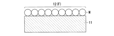
- a single particle film etching mask 12 made of a large number of particles M is formed on a mold base 11 (FIG. 6A).
- a method of forming the single particle film etching mask 12 on the mold base 11 it can be formed on the substrate by a method using a so-called LB method (Langmuir-Blodget method).
- LB method Liuir-Blodget method
- a dropping step of dropping a dispersion in which particles are dispersed in a solvent onto a liquid surface in a water tank a single particle film forming step of forming a single particle film F made of particles by volatilizing the solvent, It can be manufactured by a method having a transfer step of transferring the single particle film F onto the substrate.
- LB method Liangmuir-Blodget method
- a dispersion liquid is prepared by adding particles having a hydrophobic surface to a hydrophobic organic solvent composed of one or more of volatile solvents such as chloroform, methanol, ethanol, and methyl ethyl ketone. Further, as shown in FIG. 7A, a water tank (trough) V is prepared, and water W is added thereto as a liquid for developing particles on the liquid surface (hereinafter, also referred to as lower layer water). And a dispersion liquid is dripped at the liquid level of lower layer water (drip process). Then, the solvent as the dispersion medium is volatilized, and the particles are developed as a single layer on the liquid surface of the lower layer water, so that a two-dimensional close packed single particle film F can be formed (single particle film formation). Process).
- hydrophobic particle when a hydrophobic particle is selected as the particle, it is necessary to select a hydrophobic particle as the solvent.
- the lower layer water needs to be hydrophilic, and water is usually used as described above. By combining in this way, as will be described later, self-organization of particles proceeds, and a two-dimensional closest packed single particle film F is formed.
- hydrophilic particles and solvents may be selected. In that case, a hydrophobic liquid is selected as the lower layer water.
- the single particle film F formed on the liquid surface by the single particle film forming step is transferred onto the mold substrate 11 which is an object to be etched while being in a single layer state (transfer step).
- the mold base 11 may be planar or may include a part or all of a non-planar shape such as a curved surface, an inclination, or a step.
- the single particle film F can cover the surface of the substrate while maintaining the two-dimensional close-packed state even if the mold substrate 11 is not flat.
- a specific method for transferring the single particle film F onto the mold base 11 is not particularly limited.
- the mold base 11 Before the film F is formed, the mold base 11 is arranged in a substantially horizontal direction in the lower layer water of the water tank in advance, and after the single particle film F is formed on the liquid level, the liquid level is gradually lowered.
- the so-called LB trough method is preferably employed because even a single-particle film F having a larger area can be easily transferred onto the mold base 11 while maintaining its secondary close-packed state (Journal of Materials and Chemistry, Vol. 11, 3333 (2001), Journal of Materials and Chemistry, Vol. 12, 3268 (2002)).
- the plurality of particles M are arranged in a substantially single layer on the flat surface 11a, which is one surface of the mold base 11. That is, a single particle film F of particles M is formed on the flat surface 11a.
- the particle arranging step it is preferable to arrange a plurality of particles M on the mold base 11 in a single layer so that the deviation D (%) of the arrangement defined by the following formula (8) is 10% or less.
- A is the average particle diameter of the particle
- B is the most frequent pitch between the particle
- indicates the absolute value of the difference between A and B.
- the deviation D is more preferably 1.0 to 3.0%.
- the average particle diameter A of the particles M is the average primary particle diameter of the particles M constituting the single particle film F, and the particle size distribution obtained by the particle dynamic light scattering method is fitted to a Gaussian curve. It can obtain
- the pitch between the particles M is the distance between the vertices of two adjacent particles M in the sheet surface direction, and the most frequent pitch B is an average of these. If the particle M is spherical, the distance between the vertices of the adjacent particles M is equal to the distance between the centers of the adjacent particles M.
- the mode pitch B between the particles M is specifically obtained as follows, similarly to the mode pitch P of the recesses c1 to cn.
- an atomic force microscope image is obtained for a randomly selected region in the single particle film F and a square region whose one side is parallel to the sheet surface 30 to 40 times the most frequent pitch B between the particles M.
- an image of a region of 9 ⁇ m ⁇ 9 ⁇ m to 12 ⁇ m ⁇ 12 ⁇ m is obtained.
- this image is waveform-separated by Fourier transform to obtain an FFT image (fast Fourier transform image).
- each region is preferably selected at least 1 mm apart, more preferably 5 mm to 1 cm apart.
- the variation in pitch between the particles M in each image can be evaluated from the area of the primary peak in the profile of the FFT image.
- This misalignment D is an index indicating the degree of closest packing of the particles M. That is, a small deviation D of the arrangement of particles means that the degree of close-packing is high, the interval between the particles is controlled, and the accuracy of the arrangement is high.
- the variation coefficient of the particle diameter of the particles M is preferably 20% or less, and preferably 10% or less. More preferably, it is 5% or less.
- the pitch of the convex portions provided on the mold base 11 is equivalent to the most frequent pitch B between the particles M. If the deviation D (%) of the arrangement is small, the pitch of the convex portions is almost equal to the average particle diameter A of the particles M. Therefore, by appropriately selecting the average particle diameter A of the particles M, convex portions having a desired pitch can be accurately formed.
- the particles M can be easily arranged so that the deviation D is 10% or less by the particle arranging step. That is, an etching mask in which particles M are closely packed with a single layer can be arranged on the mold base 11 with very high accuracy.
- the single particle film F thus formed functions as the single particle etching mask 12.
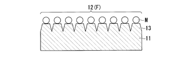
- the mold base 11 provided with the single particle etching mask 12 on one side is subjected to gas phase etching and surface processing (etching process) to form a convex portion on one side of the mold substrate.
- etching process gas phase etching and surface processing
- a convex part can be formed by continuing an etching. By changing the etching conditions halfway, a step shape can be formed on the convex portion (FIG. 6C).
- the rate at which the particles M are etched changes, and accordingly, the rate at which the mold base 11 is etched also changes.
- the particles M constituting the single particle film etching mask 12 are not particularly limited, and for example, gold particles, colloidal silica particles, and the like can be used.
- a generally used etching gas can be used.
- These particles M and etching gas can be changed according to the mold base 11 to be etched.
- a glass substrate is selected as the mold base, and these are combined, the etching gas is reactive with glass such as CF 4 or CHF 3 Is used, the etching rate of the gold particles becomes relatively slow, and the glass substrate is selectively etched.
- colloidal silica particles are selected as the particles M constituting the single particle film etching mask 12, and a PET substrate is selected as a substrate and these are combined, the etching gas is relatively soft by using an inert gas such as Ar.
- the PET substrate can be selectively physically etched.
- a step shape can be formed on the convex portion of the mold base.
- the composition is ⁇ 75: 25, it is possible to change the etching rate and form the convex portion.
- the antenna power is 1500 W
- the bias power is 50 to 300 W
- the gas flow rate is 30 to 50 sccm.
- the etching rate cannot be controlled by setting the bias power, but can be controlled by the concentration (flow rate) of the etching gas in the chamber. Therefore, by changing the concentration (flow rate) of the etching gas in the chamber, the ratio between the vertical etching and the isotropic etching can be controlled, and the step shape can be formed on the convex portion.
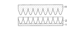
- the optical element can be transferred (odd number of times) from the mold to obtain an optical element in which a concave portion is formed in the antireflection layer 2. Since the transferred transfer object (antireflection layer having recesses) is formed on a one-to-one basis with respect to the mold, the pitch of the projections of the mold base 11 and the pitch of the recesses formed in the antireflection layer Are equal to each other, and the misalignment of the recesses formed in the antireflection layer is the same as that of the mold.
- die is not restricted to the said method.
- a photoresist mask in which a pattern is formed by interference exposure may be used instead of the single particle etching mask.
- a mold having a corresponding concave shape can be produced by changing the treatment voltage in anodizing of aluminum.
- an antireflection layer having a concave portion can be produced by transferring an even number of times from the mold.
- a flowable material is poured into a mold, and then the material is solidified to transfer the surface shape of the mold surface. The mold is pressed against a resin or glass material to transfer the surface shape.
- nanoimprinting is exemplified.
- the mold obtained by the above method has any one of the following features [1] to [3].
- [1] A plurality of minute protrusions having a most frequent pitch equal to or less than the wavelength of light in a use environment are provided on a substrate, and 80% or more of the protrusions have one or more steps, and Mold that satisfies the conditions of (However, d m is the diameter of the convex portion, w t is the sum of the width of each step in any cutting plane.).
- a plurality of minute convex portions having a most frequent pitch equal to or less than the wavelength of light under the usage environment are provided on the substrate, and 80% or more of the convex portions have two or less steps, and Mold that satisfies the conditions of (However, d m is the diameter of the convex portion, w t is the sum of the width of each step in any cutting plane.).
- the substrate is provided with a plurality of minute convex portions having a mode pitch equal to or less than the wavelength of light under the use environment, and 80% or more of the convex portions have one step, and the following conditions A mold that meets the requirements. (However, d m is the diameter of the convex portion, w t is the sum of the width of each step in any cutting plane.).
- FIG. 12 is a diagram schematically showing a cross section of this mold.
- the mold 100 includes a base 101 and a plurality of convex portions c1 ′ to cn ′.
- the mold 100 may have a flat portion f ′ corresponding to the flat portion f in FIG.
- the ratio of the convex part which has a step is judged as follows. From the AFM image of the mold 100 or the microscopic image obtained by actually cutting the mold, a cross section as shown in FIG. 12 along a line having a length of 5 ⁇ m in an arbitrary direction and position is obtained.
- the cross section is a plane perpendicular to the arrangement surface where the convex portions are arranged.
- the cutting direction for obtaining a cross section is a direction along the arrangement direction of the convex portions.
- an arbitrary portion including 30 to 40 or more convex portions is extracted, and the ratio of convex portions having steps is measured for each convex portion included therein.
- the diameter d m passes the top t1 ' ⁇ tn' of the projections can be determined as the maximum diameter of the convex portion in the cross section perpendicular to the array surface of the projection.
- the procedure described in the definition of the step width in the optical element 10 can be applied to the definition of the step width w t in the mold 100.
- the height at which the step is provided on the surface of the convex portion of the mold 100 is adjusted so that the concave portion of the optical element of the present invention has a step at a predetermined position.
- the depth at which the step on the concave surface of the optical element is formed varies depending on the transfer conditions and the material. Therefore, the optical element of the present invention can be accurately manufactured by performing a transfer test using a plurality of prototype molds with different step positions and optimizing the mold and transfer conditions.
- the antireflection performance of the optical element in the present invention was confirmed by simulation.
- a simulation method will be described (see Applied Optics, Vol. 26, No. 6, 1142-1146 (1987), Applied Optics, Vol. 32, No. 7, 1154-1167 (1993), etc.).
- the refractive index n s has a recess shape, as shown in Figure 8.
- the antireflection layer having a recess is sliced into N layers from the reference point side, and is regarded as a layer structure having the first layer,.
- the jth layer is composed of an air region having a width q and an antireflection layer region having a width 1-q.
- the width at this time is the width of the interface with the (j ⁇ 1) th layer.
- the j-th effective refractive index in the layer n j, the thickness of this layer was d j.
- n j can be obtained from the refractive indexes n 0 , n s and the width q. d j can be determined by dividing the modal depth of the recess in the number of layers N.
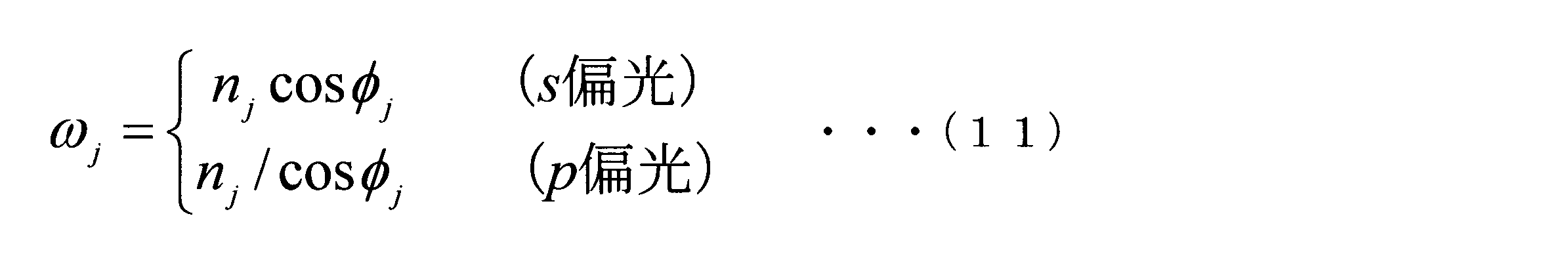
- ⁇ j and ⁇ j are the following expressions (10) and (11).
- Example 1 Assuming that the concave portion has one step, the average reflectance was obtained while changing the total step width w s and the average step depth z s . At this time, the depth h of the recesses was 295 nm (average value), the most frequent pitch P was 120 nm, and the diameter d was 120 nm (average value). Light was incident from an air with a refractive index of 1.0 to an interface with a refractive index of 1.5 at an incident angle of 5 °, and the refractive index of the material of the antireflection layer was also set to 1.5. The results are shown in Table 1. The average reflectance was determined as follows.
- Equation (13) the reflectance of light when light having a wavelength of 380 nm is incident at an incident angle of 5 ° is calculated from Equation (13). Thereafter, the reflectance when light of each wavelength is incident up to 780 nm in increments of 20 nm is similarly calculated from equation (13). The average value of the reflectance of light of each wavelength was determined and used as the average reflectance.
- Example 2 Even in the case of two steps, the average reflectance was obtained while changing the total step width w s and the average step depth z s in the same manner as in Example 1.
- the horizontal width of each step was w s / 4, and the vertical width was 0.1 h / 2.
- Table 2 The results are shown in Table 2. At this time, the calculation conditions of the depth of the concave portion, the mode pitch, the diameter, and the reflectance were the same as those in Example 1.
- Example 3 Even in the case of three steps, the average reflectance was obtained while changing the total step width w s and the average step depth z s in the same manner as in Example 1.
- the horizontal width of each step was w s / 6 and the vertical width was 0.1 h / 3.
- Table 3 The results are shown in Table 3. At this time, the calculation conditions of the depth of the concave portion, the mode pitch, the diameter, and the reflectance were the same as those in Example 1.
- the average reflectance at the same w s and z s is compared.
- the average reflectance in Table 2 is lower than the average reflectance in Table 3. That is, in this range, the average reflectance is lower in the case of two steps (Table 2) than in the case of three steps (Table 3). That is, in the range of 0.10d ⁇ w s ⁇ 0.20d and 0.44h ⁇ z s ⁇ 0.56h, the case of two steps is superior in terms of average reflectance than the case of three steps. And the number of steps can be two or less.
- Tables 1 and 2 average reflectances at the same w s and z s are compared.
- the average reflectance in Table 1 is lower than the average reflectance in Table 2. That is, in this range, the average reflectance is lower when the number of steps is one (Table 1) than when the number of steps is two (Table 2). That is, in the range of 0.09d ⁇ w s ⁇ 0.15d and 0.44h ⁇ z s ⁇ 0.56h, the case of one step is superior in terms of average reflectance than the case of two steps.
- the number of steps can be one.
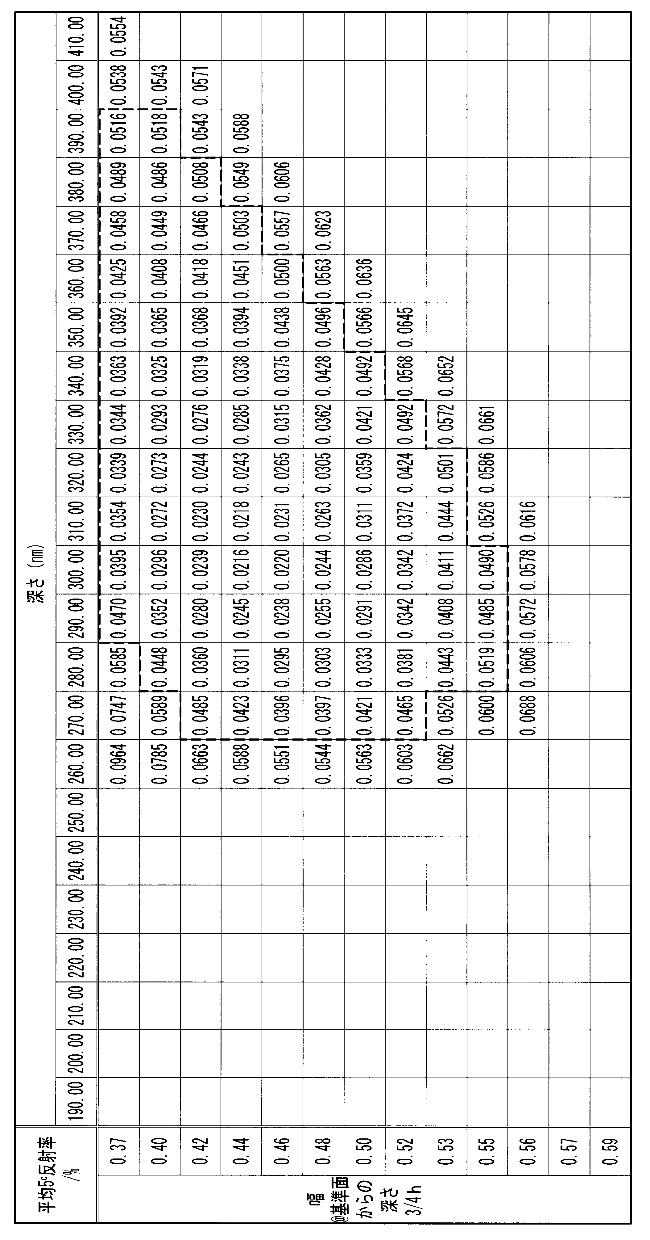
- Example 4 the shape of the envelope surface of the recess was changed to obtain the average reflectance.
- the shape of the envelope surface was changed by changing the depth of the recess and the width d 3/4 of the recess at a depth of 3/4 h from the reference plane including the reference point.
- Recess has one step, to fix the total w s of the width of the step a mean value z s depth position of 0.14d and steps 0.48H.
- the most frequent pitch P of the recesses was 90 nm, and the diameter d was 90 nm (average value).
- Table 4 The row in Table 4 is the ratio of the width d 3/4 of the recess at a depth of 3/4 h from the reference plane including the reference point with respect to the diameter d of the recess, and the column is the mode depth h of the recess.
- Example 5 The average reflectance was determined in the same manner as in Example 4 except that the most frequent pitch of the recesses was 120 nm and the diameter was 120 nm (average value). The results are shown in Table 5.
- the row in Table 5 is the ratio of the width d 3/4 of the recess at the depth of the reference surface 3 / 4h to the diameter d of the recess, and the column is the mode depth h of the recess.
- Example 6 The average reflectance was determined in the same manner as in Example 4 except that the most frequent pitch of the recesses was 200 nm and the diameter was 200 nm (average value). The results are shown in Table 6.
- the row in Table 6 is the ratio of the width d 3/4 of the recess at the depth of the reference plane 3 / 4h to the diameter d of the recess, and the column is the mode depth h of the recess.
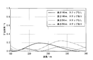
- the area surrounded by the dotted line shows an average reflectance that is not more than half of the average reflectance (0.1047) when there is no step, and has high antireflection performance.
- the shape of the envelope surface in this range is a weight shape from the relationship between the depth of the recess and the width d 3/4 of the recess at a depth of 3/4 h from the reference surface.
- Example 7 The change in average reflectance according to the wavelength of incident light was determined. Recess has one step, to fix the total w s of the width of the step a mean value z s depth of 0.14d and steps 0.48H. The most frequent pitch P of the recesses was 120 nm, and the diameter d was 120 nm.
- Light was incident from an air with a refractive index of 1.0 to an interface with a refractive index of 1.5 at an incident angle of 5 °, and the refractive index of the material of the antireflection layer was also set to 1.5.
- FIG. 9 shows the result when the wavelength in the visible light region is incident
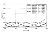
- FIG. 10 shows the result when the light having the wavelength in the near infrared region is incident
- FIG. 11 shows the result when the wavelength in the near ultraviolet region is incident. .
- the concave portion has no step and the most frequent depth of the concave portion is 140 nm and 295 nm was also obtained. From FIG. 11, it can be seen that even when near ultraviolet light is incident, particularly high antireflection performance is exhibited when the mode depth is 45 to 55% of the median value in the wavelength range of the incident light.
Abstract
Description
本願は、2014年7月15日に、日本に出願された特願2014-144989号と、2015年4月7日に、日本に出願された特願2015-078526号とに基づき優先権を主張し、その内容をここに援用する。
例えば特許文献1では、凸部又は凹部に二つ以上のステップを設けることにより、光学素子の反射防止性能を向上させることが記載されている。凸部又は凹部に二つ以上のステップを設けると、モスアイ構造による屈折率が連続的に変化する界面の中に、不連続界面が生じる。この不連続界面は、入射した光の一部を反射する。この不連続界面で反射した光同士を干渉させることで、反射光を低減することが特許文献1では提案されている。
その結果、所定の範囲に凹部のステップの幅や位置を設ければよいことを見出した。
〔1〕基体上に、使用環境下の光の波長以下の最頻ピッチを有する複数の微小な凹部が形成された反射防止層を備え、前記凹部の80%以上が、1つ以上のステップを有し、かつ以下の条件を満たすことを特徴とする光学素子;(ただし、dは前記凹部の直径であり、hは前記凹部の深さであり、wsは任意の切断面における各ステップの幅の合計であり、zsはこれら各ステップの深さの平均値である。)。


〔5〕前記ステップを有する凹部の包絡面が、錘形状であることを特徴とする〔1〕~〔4〕のいずれか一項に記載の光学素子。
〔6〕隣接する7つの前記凹部の中心点が正六角形の6つの頂点と対角線の交点となる位置関係で連続して整列しているエリアを複数備え、該複数のエリアの面積、形状および格子方位がランダムであることを特徴とする〔1〕~〔5〕のいずれか一項に記載の光学素子。
図1におけるt1~tnは各凹部c1~cnの中心点である。AFM(原子間力顕微鏡)の測定結果に基づき、基準面と平行に各凹部について20nm毎に複数の等高線を引き、各等高線の重心点(x座標とy座標で決定される点)を求める。これらの各重心点の平均位置(各x座標の平均とy座標の平均で決定される位点)が、該凹部の中心点である。
図1におけるm1~mnは、AFMで求めた隣接する中心点の中点である。平坦面fは、AFMの測定結果に基づき、その領域内の中点における位置座標と、その領域内における任意の点の位置座標とを結ぶ直線の、AFMの基準面に対する傾きが±10゜以下である領域である。基準面は測定領域における基体面と平行な面で、後述する基準点を通る面とした。
まず、基体1上における無作為に選択された領域で、一辺が最頻ピッチPの30~40倍の正方形の領域について、AFMイメージを得る。例えば、最頻ピッチが300nm程度の場合、9μm×9μm~12μm×12μmの領域のイメージを得る。そして、このイメージをフーリエ変換により波形分離し、FFT像(高速フーリエ変換像)を得る。ついで、FFT像のプロファイルにおける0次ピークから1次ピークまでの距離を求める。
こうして求められた距離の逆数がこの領域における最頻ピッチPである。このような処理を無作為に選択された合計25カ所以上の同面積の領域について同様に行い、各領域における最頻ピッチを求める。こうして得られた25カ所以上の領域における最頻ピッチP1~P25の平均値が最頻ピッチPである。この際、各領域同士は、少なくとも1mm離れて選択されることが好ましく、より好ましくは5mm~1cm離れて選択される。
各エリアC1~Cnは、隣接する7つの凹部の中心点が正六角形の6つの頂点と対角線の交点となる位置関係で連続して整列している領域である。図3では、各凹部の中心点の位置を、便宜上、その中心点を中心とする円uで示している。
本発明において、隣接する7つの凹部の中心点が正六角形の6つの頂点と対角線の交点となる位置関係とは、具体的には、以下の条件を満たす関係をいう。
まず、1つの中心点t1から隣接する中心点t2の方向に、長さが最頻ピッチPと等しい長さの線分L1を引く。次いで中心点t1から、線分L1に対して、60゜、120゜、180゜、240゜、300゜の各方向に、最頻ピッチPと等しい長さの線分L2~L6を引く。中心点t1に隣接する6つの中心点が、中心点t1と反対側における各線分L1~L6の終点から、各々最頻ピッチPの15%以内の範囲にあれば、これら7つの中心点は、正六角形の6つの頂点と対角線の交点となる位置関係にある。
最頻ピッチPが500nm未満の時、10μm×10μmのAFMイメージ測定範囲内における最頻面積Qは、0.026μm2~6.5μm2であることが好ましい。
最頻ピッチPが500nm以上1μm未満の時、10μm×10μmのAFMイメージ測定範囲内における最頻面積Qは、0.65μm2~26μm2であることが好ましい。
最頻ピッチPが1μm以上の時、50μm×50μmのAFMイメージ測定範囲内における最頻面積Qは、2.6μm2~650μm2であることが好ましい。
最頻面積Qが好ましい範囲内であれば、反射防止性能の視野角依存性が高くなる問題を防止しやすい。
面積のランダム性の度合いは、具体的には、以下の条件を満たすことが好ましい。
まず、ひとつのエリアの境界線が外接する最大面積の楕円を描き、その楕円を下記式(7)で表す。

最頻ピッチPが500nm以上1μm未満の時、10μm×10μmのAFMイメージ測定範囲内におけるπabの標準偏差は、1.95μm2以上であることが好ましい。
最頻ピッチPが1μm以上の時、50μm×50μmのAFMイメージ測定範囲内におけるπabの標準偏差は、8.58μm2以上であることが好ましい。
πabの標準偏差が好ましい範囲内であれば、反射光の平均化の効果に優れ、反射防止性能の視野角依存性が高くなる問題を防止しやすい。
各エリアC1~Cnの格子方位のランダム性は、具体的には、以下の条件を満たすことが好ましい。
まず、任意のエリア(I)における任意の隣接する2つの凹部の中心点を結ぶ直線K0を画く。次に、該エリア(I)に隣接する1つのエリア(II)を選択し、そのエリア(II)における任意の凹部と、その凹部に隣接する6つの凹部の中心点を結ぶ6本の直線K1~K6を画く。直線K1~K6が、直線K0に対して、いずれも3度以上異なる角度である場合、エリア(I)とエリア(II)との格子方位が異なる、と定義する。
エリア(I)に隣接するエリアの内、格子方位がエリア(I)の格子方位と異なるエリアが2以上存在することが好ましく、3以上存在することが好ましく、5以上存在することがさらに好ましい。
FFT基本波の最大値と最小値の比が大きい場合は、凹部の格子方位が揃っており、凹部を2次元結晶とみなした場合、単結晶性が高い構造と言える。反対に、FFT基本波の最大値と最小値の比が小さい場合は、凹部の格子方位が揃っておらず、凹部を2次元結晶とみなした場合は多結晶構造であると言える。


凹部の形状が確認しにくい場合は、光学素子をモールドとして反転転写した転写品の凸部の形状を確認することにより、凹部の形状(深さ、ステップ位置を含む)を確認してもよい。この際、転写品の断面は、AFMイメージを測定してもよいし、切断面を顕微鏡で直接観察してもよい。転写品の頂部を通る切断面を得る点から、切断面はAFMイメージにより測定することが好ましい。
この断面の凹部が30個~40個以上含まれる任意の部分を抽出し、その中に含まれる各凹部について、ステップを有する凹部の割合を測定する。
直径dは、凹部の配列面に垂直な断面を観測した際の凹部における最大径として求めることができる。
深さhは、凹部の配列面に垂直な断面を観測した際の凹部における最深点と最も高い部位(切断面において最深点から最も離れた部分:以下「基準点」という)との高さの差を求めることで得られる。
まずステップは、以下の手順で設定する。凹部c1~cnは、包絡面の形状において、作用効果上無視できる程度の微細な凹凸を有する場合があり、そのような微細な凹凸は無視した上で設定するものとする。具体的には、凹部のフィッティング曲線に対して、凹部c1~cnの深さhの3%以下の変化は無視する。
(ア)広義の変曲点を求める。
(イ)変曲点のそれぞれに接線を引く。
(ウ)接線の交点に最も近い点を変化点とする。
(エ)各変化点同士を直線で結ぶ。最も最深点に近い変化点は、次の変化点がないため、変化点における接線を引く。こうして得られた直線を基準点(凹部断面の最も高い部位)に近いものから第1直線、第2直線、・・・とする。
(オ)これらの直線のうち第n直線の傾きの絶対値が、第n-1直線の傾きおよび第n+1直線の傾きの絶対値以下である場合、この第n直線の区間を「ステップ」と定義する。
上記(ア)~(オ)の手順を、図4A~図4Dを用いて説明する。図4A~図4Dはステップの定義を説明するための模式図である。
ステップの幅は、図5で示すように、前述のように定義されたステップを凹部の基準面への射影した幅を意味する。すなわち、図5において、第1ステップの幅はw1である。ステップの幅の合計は、これら各ステップの幅の合計であり、ステップの幅の合計wsは、w1+w2+w3の2倍の値となる。2倍の値となるのは、ステップは同じ深さにおいて、凹部の周方向に同等に形成されるためである。すなわち、図5では1つの基準点から最深点までの間にあるステップのみを示しているが、凹部の最深点を通る任意の断面で切断した際に、ステップは1つの基準点から最深点までの間と、最深点からもう一つの基準点までの間にも存在するため2倍となる。
ステップの深さは、基準点を含む基準面からステップの中点までの深さを意味する。すなわち、例えば図4Dで定義された第1ステップの深さはz1となる。「ステップの高さの平均値zs」は、図5において(z1+z2+z3)/3を意味する。このとき、ステップの幅と異なり2倍の値とならないのは、zsは平均値であるためである。


光学素子10は、三角格子状に凹部が配列する場合、その三角格子状に形成された3個の凹部に囲まれた領域に、突起部を有することが好ましい。ここで、突起部とは、基体と反対側に、平均基準面よりも突出している部分を示す。平均基準面とは、AFMまたは顕微鏡を用いて得られた図1のような断面における30個~40個以上の凹部における各凹部における基準点の高さ(基体に対して鉛直方向の高さ)を平均した平均点を通り、基体と平行な面を意味する。同様に、光学素子10は、正方格子状に凹部が配列する場合、凹部4個に囲まれた領域に突起部を有することが好ましい。
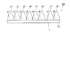
以下に、光学素子の製造方法について説明する。本発明の光学素子は、所定の形状を有する金型を奇数回転写することで得ることができる。この金型は、多数の粒子Mを2次元的に配列させたエッチングマスクを用いることで作製することができる。図6A~Dは、本発明の光学素子の製造方法を模式的に示した図である。
以下に各工程について具体的に説明する。
まず、クロロホルム、メタノール、エタノール、メチルエチルケトンなどの揮発性の高い溶剤のうちの1種以上からなる疎水性の有機溶剤中に、表面が疎水性の粒子を加えて分散液を調製する。また、図7Aに示すように水槽(トラフ)Vを用意し、これに、その液面上で粒子を展開させるための液体(以下、下層水という場合もある。)として水Wを入れる。
そして、分散液を下層水の液面に滴下する(滴下工程)。すると、分散媒である溶剤が揮発するとともに、粒子が下層水の液面上に単層で展開し、2次元的に最密充填した単粒子膜Fを形成することができる(単粒子膜形成工程)。
図7Bで示すように、単粒子膜形成工程により液面上に形成された単粒子膜Fを、単層状態のままエッチング対象物である金型基体11上に移し取る(移行工程)。金型基体11は平面状でもよく、曲面、傾斜、段差等の非平面形状を一部もしくは全部に含んでいても良い。単粒子膜Fは、金型基体11が平面でなくても2次元的な最密充填状態を維持しつつ基体表面を被覆することが可能である。単粒子膜Fを金型基体11上に移し取る具体的な方法には特に制限はなく、例えば、疎水性の金型基体11を単粒子膜Fに対して略平行な状態に保ちつつ、上方から降下させて単粒子膜Fに接触させ、ともに疎水性である単粒子膜Fと金型基体11との親和力により、単粒子膜Fを金型基体11に移行させ、移し取る方法;単粒子膜Fを形成する前にあらかじめ水槽の下層水内に金型基体11を略水平方向に配置しておき、単粒子膜Fを液面上に形成した後に液面を徐々に降下させることにより、金型基体11上に単粒子膜Fを移し取る方法などがある。これらの方法によれば、特別な装置を使用せずに単粒子膜Fを金型基体11上に移し取ることができる。より大面積の単粒子膜Fであっても、その2次的な最密充填状態を維持したまま金型基体11上に移し取りやすい点で、いわゆるLBトラフ法を採用することが好ましい(Journal of Materials and Chemistry, Vol.11, 3333 (2001)、Journal of Materials and Chemistry, Vol.12, 3268 (2002)など参照。)。
粒子配列工程では、下記式(8)で定義される配列のずれD(%)が10%以下となるように、金型基体11に複数の粒子Mを単一層で配列させることが好ましい。
ずれDは、1.0~3.0%であることがより好ましい。
一方、粒子M間のピッチとは、シート面方向における隣り合う2つの粒子Mの頂点と頂点の距離であり、最頻ピッチBとはこれらを平均したものである。粒子Mが球形であれば、隣り合う粒子Mの頂点と頂点との距離は、隣り合う粒子Mの中心と中心の距離と等しい。
まず、単粒子膜Fにおける無作為に選択された領域で、一辺が粒子M間の最頻ピッチBの30~40倍のシート面と平行な正方形の領域について、原子間力顕微鏡イメージを得る。例えば粒径300nmの粒子Mを用いた単粒子膜Fの場合、9μm×9μm~12μm×12μmの領域のイメージを得る。そして、このイメージをフーリエ変換により波形分離し、FFT像(高速フーリエ変換像)を得る。ついで、FFT像のプロファイルにおける0次ピークから1次ピークまでの距離を求める。こうして求められた距離の逆数がこの領域における最頻ピッチB1である。このような処理を無作為に選択された合計25カ所以上の同面積の領域について同様に行い、各領域における最頻ピッチB1~B25を求める。こうして得られた25カ所以上の領域における最頻ピッチB1~B25の平均値が式(8)における最頻ピッチBである。この際、各領域同士は、少なくとも1mm離れて選択されることが好ましく、より好ましくは5mm~1cm離れて選択される。
この際、FFT像のプロファイルにおける1次ピークの面積から、各イメージについて、その中の粒子M間のピッチのばらつきを評価することもできる。
配列のずれD(%)を10%以下とするため、粒子Mの粒径の変動係数(標準偏差を平均値で除した値)は、20%以下であることが好ましく、10%以下であることがより好ましく、5%以下であることがさらに好ましい。
金型基体11に設けられる凸部のピッチは、粒子M間の最頻ピッチBと同等となる。配列のずれD(%)が小さければ、凸部のピッチは、粒子Mの平均粒径Aとほぼ同等となる。そのため、粒子Mの平均粒径Aを適切に選択することにより、所望のピッチの凸部を精度良く形成することができる。
このように形成された単粒子膜Fが単粒子エッチングマスク12として機能する。単粒子エッチングマスク12が片面に設けられた金型基体11を、気相エッチングして表面加工する(エッチング工程)ことにより、金型基板の片面に凸部を形成する。具体的には、気相エッチングを開始すると、まず図6Bに示すように、エッチングマスク12を構成している粒子Mの隙間をエッチングガスが通り抜けて金型基体11の表面に到達し、その部分に溝が形成され、各粒子Mに対応する位置にそれぞれ円柱13が現れる。このとき、気相エッチングにより各円柱13上の粒子Mも徐々にエッチングされて小さくなる。さらにエッチングを続けることにより、凸部を形成することができる。エッチングの条件を途中で変更することで、凸部にステップ形状を形成することができる(図6C)。エッチング条件を変更すると、粒子Mがエッチングされる速度が変化し、それに伴い金型基体11をエッチングする速度も変化する。
これらの粒子Mおよびエッチングガスは、エッチングされる金型基体11に合わせて変更することができる。例えば単粒子膜エッチングマスクを構成する粒子として金粒子を選択し、金型基体としてガラス基板を選択してこれらを組み合わせた場合、エッチングガスにCF4、CHF3などのガラスと反応性のあるものを用いると、金粒子のエッチング速度が相対的に遅くなり、ガラス基板のほうが選択的にエッチングされる。
単粒子膜エッチングマスク12を構成する粒子Mとしてコロイダルシリカ粒子を選択し、基体としてPET基板を選択してこれらを組み合わせた場合、エッチングガスにArなどの不活性ガスを用いることで、比較的柔らかいPET基板を選択的に物理エッチングすることができる。
一方で、基板の材質とエッチングガスの種類の組み合わせによるが、気相エッチングでは、プラズマによって生成したラジカルによる等方性エッチングも並行して起こる。ラジカルによるエッチングは化学エッチングであり、エッチング対象物のどの方向にも等方的なエッチングが生じる。
ラジカルは電荷を持たないためバイアスパワーの設定でエッチング速度をコントロールすることはできないが、エッチングガスのチャンバー内濃度(流量)で操作することができる。そのため、エッチングガスのチャンバー内濃度(流量)を変化させることでも垂直エッチングと等方エッチングの割合を制御することができ、凸部にステップ形状を形成することができる。
金型の作製方法は、当該方法に限られない。例えば、単粒子エッチングマスクの代わりに、干渉露光によりパターンが形成されたフォトレジストマスクを用いても良い。アルミの陽極酸化において処理電圧を変更することで、対応する凹形状を有するモールドを作製することもできる。この場合、当該モールドから偶数回転写することにより凹部を有する反射防止層を作製することができる。
上述の転写方法としては、成形型に流動性の材料を流し込んだ後、材料を固化して成形型表面の表面形状を転写する射出成形、金型を樹脂やガラス材料に押し付けて表面形状を転写する所謂ナノインプリントなどが挙げられる。
[1] 基体上に、使用環境下の光の波長以下の最頻ピッチを有する複数の微小な凸部を備え、前記凸部の80%以上が、1つ以上のステップを有し、かつ以下の条件を満たすものである金型。
(ただし、dmは前記凸部の直径であり、wtは任意の切断面における各ステップの幅の合計である。)。
(ただし、dmは前記凸部の直径であり、wtは任意の切断面における各ステップの幅の合計である。)。

(ただし、dmは前記凸部の直径であり、wtは任意の切断面における各ステップの幅の合計である。)。

ステップを有する凸部の割合は以下のように判断する。金型100のAFMイメージまたは実際に金型を切断した顕微鏡画像から、任意の方向と位置における長さ5μmの線に沿った図12のような断面を得る。断面は、凸部が配列する配列面に垂直な面である。凸部が規則的に配列している場合は、断面を得るための切断方向を凸部の配列方向に沿った方向とすることが好ましい。
直径dmは、凸部の頂部t1’~tn’を通り、凸部の配列面に垂直な断面における凸部の最大径として求めることができる。
金型100の凸部表面においてステップを設ける高さは、本発明の光学素子の凹部が所定の位置にステップを有するように調整される。
金型を用いた射出成形またはインプリントにおいて、光学素子の凹部表面のステップが形成される深さは、転写条件および材料によって変化する。そのため、ステップの位置を変えた複数の試作金型を用いて転写テストを行い、金型および転写条件の最適化を行うことにより、本発明の光学素子を精度よく製造することができる。
屈折率n0の物質と、屈折率nsの物質の界面への光が入射した際の反射について考える。このとき屈折率nsの物体は、図8で示すように凹部形状を有する。
まず図8に示すように、凹部を有する反射防止層を基準点側からN層に分けてスライスし、基準点側から第1層、・・・第N層までを有する層構造とみなす。第j番目の層は、幅qの空気の領域と幅1-qの反射防止層の領域が繰り返してなる。このときの幅は第j-1層との界面の幅とする。この第j番目の層における実効屈折率をnj、この層の厚さをdjとした。このとき、njは屈折率n0、nsおよび幅qから求めることができる。djは、凹部の最頻深さを層数Nで割ることで求めることができる。


凹部が一つのステップを有するとして、ステップの幅の合計wsおよびステップの深さの平均値zsを変更しながら平均反射率を求めた。このとき凹部の深さhは295nm(平均値)、最頻ピッチPは120nm、直径dは120nm(平均値)とした。光は屈折率1.0の空気から、屈折率1.5の界面に入射角5°で入射するものとし、反射防止層の材料の屈折率も1.5とした。その結果を表1に示す。
平均反射率は以下のように求めた。まず、波長380nmの光を入射角5°で入射した際の光の反射率を、式(13)から計算する。その後、20nm刻みで780nmまで各波長の光を入射した際の反射率を、同様に式(13)から計算する。これら各波長の光の反射率の平均値を求め、平均反射率とした。

0.12d≦ws≦0.17dおよび0.42h≦zs≦0.52hを満たす領域は、ステップを有さない場合の平均反射率(0.1047)と比べても、半分以下の平均反射率となり非常に優れた反射防止性能を有することが分かる。
ステップが2つの場合においても、実施例1と同様にステップの幅の合計wsおよびステップの深さの平均値zsを変更しながら平均反射率を求めた。このとき、2つのステップは、典型的な例としてzs=aとしたときに0.75aおよび1.25aの位置に存在するものとした。すなわち、例えばzs=0.40hとしたときは、2つのステップは0.30hおよび0.50hの位置に存在するものとした。また各ステップの横幅はws/4、縦幅は0.1h/2とした。その結果を表2に示す。このとき凹部の深さ、最頻ピッチ、直径および反射率の計算条件は実施例1と同じとした。
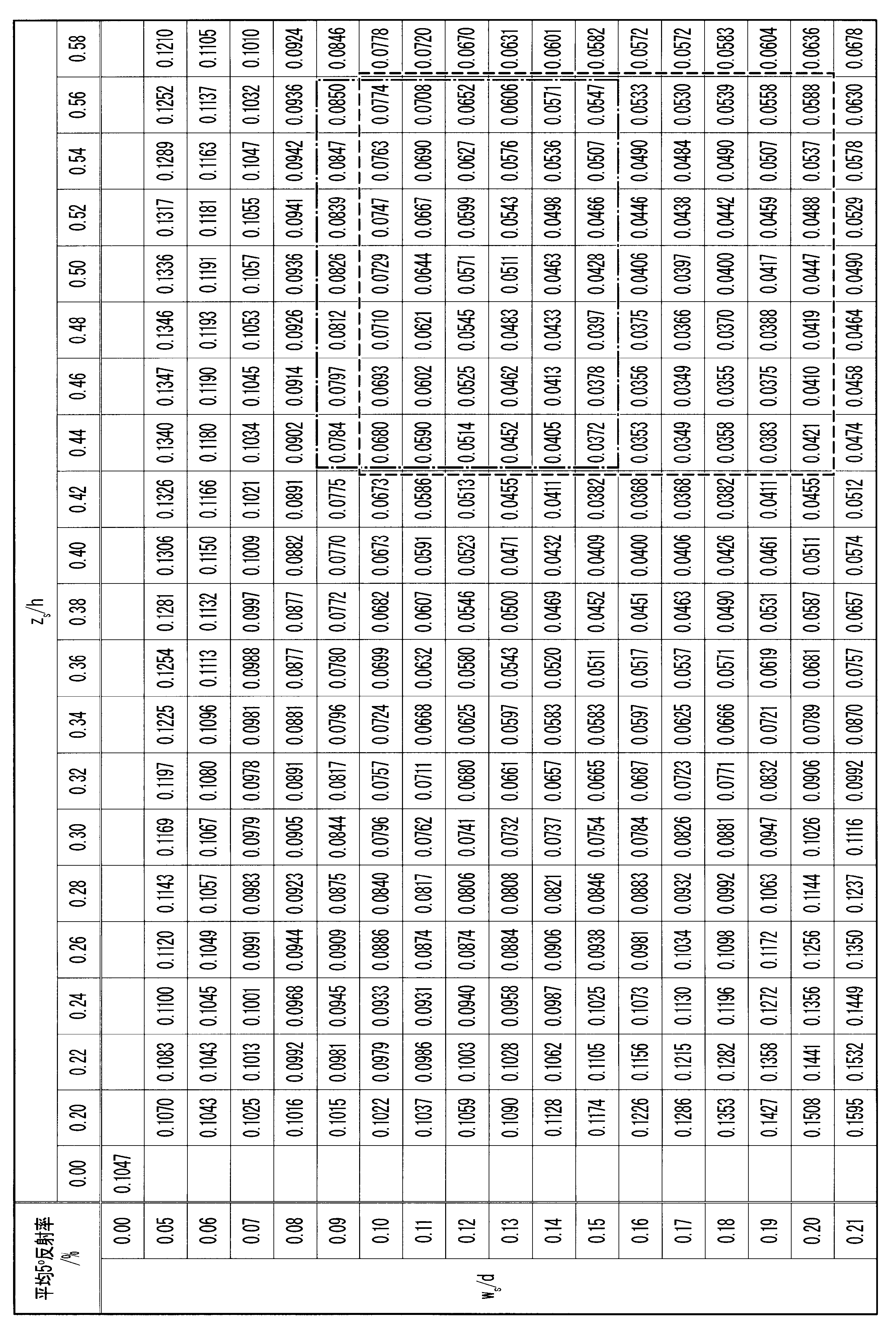
ステップが3つの場合においても、実施例1と同様にステップの幅の合計wsおよびステップの深さの平均値zsを変更しながら平均反射率を求めた。このとき、3つのステップは、典型的な例としてzs=aとしたときに0.5a、1.0a、1.5aの位置に存在するものとした。すなわち、例えばzs=0.40hとしたときは、3つのステップは0.20h、0.40h、0.60hの位置に存在するものとした。また各ステップの横幅はws/6、縦幅は0.1h/3とした。その結果を表3に示す。このとき凹部の深さ、最頻ピッチ、直径および反射率の計算条件は実施例1と同じとした。

つまり、0.10d≦ws≦0.20d、かつ0.44h≦zs≦0.56hの範囲では、ステップが2つの場合の方が、ステップが3つの場合より平均反射率の面で優れており、ステップの数を2つ以下とすることができる。
つまり、0.09d≦ws≦0.15d、かつ0.44h≦zs≦0.56hの範囲では、ステップが1つの場合の方が、ステップが2つの場合より平均反射率の面で優れており、ステップの数を1つとすることができる。
次に凹部の包絡面の形状を変更して平均反射率を求めた。凹部の深さと、基準点を含む基準面から3/4hの深さでの凹部の幅d3/4を変更することで、包絡面の形状を変更した。
凹部は、一つのステップを有し、ステップの幅の合計wsを0.14dおよびステップの深さ位置の平均値zsを0.48hで固定した。また凹部の最頻ピッチPは90nm、直径dは90nm(平均値)とした。光は屈折率1.0の空気から、屈折率1.5の界面に入射角5°で入射するものとし、反射防止層の材料の屈折率も1.5とした。その結果を表4に示す。表4における行は凹部の直径dに対する基準点を含む基準面から3/4hの深さでの凹部の幅d3/4の割合であり、列は凹部の最頻深さhである。

凹部の最頻ピッチを120nm、直径を120nm(平均値)としたこと以外は、実施例4と同様にして、平均反射率を求めた。その結果を表5に示す。表5における行は凹部の直径dに対する基準面3/4hの深さでの凹部の幅d3/4の割合であり、列は凹部の最頻深さhである。

凹部の最頻ピッチを200nm、直径を200nm(平均値)としたこと以外は、実施例4と同様にして、平均反射率を求めた。その結果を表6に示す。表6における行は凹部の直径dに対する基準面3/4hの深さでの凹部の幅d3/4の割合であり、列は凹部の最頻深さhである。
入射する光の波長による平均反射率の変化を求めた。
凹部は、1つのステップを有し、ステップの幅の合計wsを0.14dおよびステップの深さの平均値zsを0.48hで固定した。凹部の最頻ピッチPは120nm、直径dは120nmとした。光は屈折率1.0の空気から、屈折率1.5の界面に入射角5°で入射するものとし、反射防止層の材料の屈折率も1.5とした。
可視光領域の波長を入射した際の結果を図9に、近赤外領域の波長の光を入射した際の結果を図10に、近紫外の波長を入射した際の結果を図11に示す。
図10では、凹部の最頻深さが、295nm、650nmの場合を求めた。比較のため、凹部がステップを有さない場合で、凹部の最頻深さが295nm、650nmの場合も求めた。この図10から、近赤外光を入射しても、最頻深さが入射した光の波長範囲における中央値の45~55%の際に、特に高い反射防止性能を示していることが分かる。
図11では、凹部の最頻深さが、140nm、295nmの場合を求めた。また比較のため、凹部がステップを有さない場合で、凹部の最頻深さが140nm、295nmの場合も求めた。この図11から、近紫外光を入射しても、最頻深さが入射した光の波長範囲における中央値の45~55%の際に、特に高い反射防止性能を示していることが分かる。
Claims (12)
- 基体上に、使用環境下の光の波長以下の最頻ピッチを有する複数の微小な凹部が形成された反射防止層を備え、
前記凹部の80%以上が、1つ以上のステップを有し、かつ以下の条件を満たす光学素子;
(ただし、dは前記凹部の直径であり、hは前記凹部の深さであり、wsは任意の切断面における各ステップの幅の合計であり、zsはこれら各ステップの深さの平均値である。)。


- 基体上に、使用環境下の光の波長以下の最頻ピッチを有する複数の微小な凹部が形成された反射防止層を備え、
前記凹部の80%以上が、2つ以下のステップを有し、かつ以下の条件を満たす光学素子;
(ただし、dは前記凹部の直径であり、hは前記凹部の深さであり、wsは任意の切断面における各ステップの幅の合計であり、zsはこれら各ステップの深さの平均値である。)。


- 基体上に、使用環境下の光の波長以下の最頻ピッチを有する複数の微小な凹部が形成された反射防止層を備え、
前記凹部の80%以上が、1つのステップを有し、かつ以下の条件を満たす光学素子;
(ただし、dは前記凹部の直径であり、hは前記凹部の深さであり、wsは任意の切断面における各ステップの幅の合計であり、zsはこれら各ステップの深さの平均値である。)。


- 前記凹部の最頻深さが、使用環境下の光の波長範囲における中央値の45~55%の範囲内にある請求項1に記載の光学素子。
- 前記ステップを有する凹部の包絡面が、錘形状である請求項1に記載の光学素子。
- 隣接する7つの前記凹部の中心点が正六角形の6つの頂点と対角線の交点となる位置関係で連続して整列しているエリアを複数備え、
該複数のエリアの面積、形状および格子方位がランダムである請求項1に記載の光学素子。 - 前記凹部の最頻深さが、使用環境下の光の波長範囲における中央値の45~55%の範囲内にある請求項2に記載の光学素子。
- 前記ステップを有する凹部の包絡面が、錘形状である請求項2に記載の光学素子。
- 隣接する7つの前記凹部の中心点が正六角形の6つの頂点と対角線の交点となる位置関係で連続して整列しているエリアを複数備え、
該複数のエリアの面積、形状および格子方位がランダムである請求項2に記載の光学素子。 - 前記凹部の最頻深さが、使用環境下の光の波長範囲における中央値の45~55%の範囲内にある請求項3に記載の光学素子。
- 前記ステップを有する凹部の包絡面が、錘形状である請求項3に記載の光学素子。
- 隣接する7つの前記凹部の中心点が正六角形の6つの頂点と対角線の交点となる位置関係で連続して整列しているエリアを複数備え、
該複数のエリアの面積、形状および格子方位がランダムである請求項3に記載の光学素子。
Priority Applications (5)
| Application Number | Priority Date | Filing Date | Title |
|---|---|---|---|
| KR1020167037036A KR20170013358A (ko) | 2014-07-15 | 2015-06-30 | 광학 소자 |
| EP15822124.2A EP3182178B1 (en) | 2014-07-15 | 2015-06-30 | Optical element |
| CN201580037275.5A CN106662674B (zh) | 2014-07-15 | 2015-06-30 | 光学元件 |
| US15/322,982 US10073193B2 (en) | 2014-07-15 | 2015-06-30 | Optical element |
| JP2016534355A JP6418240B2 (ja) | 2014-07-15 | 2015-06-30 | 光学素子 |
Applications Claiming Priority (4)
| Application Number | Priority Date | Filing Date | Title |
|---|---|---|---|
| JP2014-144989 | 2014-07-15 | ||
| JP2014144989 | 2014-07-15 | ||
| JP2015-078526 | 2015-04-07 | ||
| JP2015078526 | 2015-04-07 |
Publications (1)
| Publication Number | Publication Date |
|---|---|
| WO2016009826A1 true WO2016009826A1 (ja) | 2016-01-21 |
Family
ID=55078324
Family Applications (1)
| Application Number | Title | Priority Date | Filing Date |
|---|---|---|---|
| PCT/JP2015/068814 WO2016009826A1 (ja) | 2014-07-15 | 2015-06-30 | 光学素子 |
Country Status (7)
| Country | Link |
|---|---|
| US (1) | US10073193B2 (ja) |
| EP (1) | EP3182178B1 (ja) |
| JP (1) | JP6418240B2 (ja) |
| KR (1) | KR20170013358A (ja) |
| CN (1) | CN106662674B (ja) |
| TW (1) | TWI660192B (ja) |
| WO (1) | WO2016009826A1 (ja) |
Cited By (1)
| Publication number | Priority date | Publication date | Assignee | Title |
|---|---|---|---|---|
| JP2021162728A (ja) * | 2020-03-31 | 2021-10-11 | デクセリアルズ株式会社 | 光学体、光学体の製造方法及び光学デバイス |
Families Citing this family (5)
| Publication number | Priority date | Publication date | Assignee | Title |
|---|---|---|---|---|
| CN104827191A (zh) * | 2015-05-12 | 2015-08-12 | 大族激光科技产业集团股份有限公司 | 蓝宝石的激光切割方法 |
| JP6784487B2 (ja) | 2015-10-30 | 2020-11-11 | デクセリアルズ株式会社 | 光学体、および表示装置 |
| DE112018003564T5 (de) * | 2017-07-11 | 2020-03-26 | Ngk Insulators, Ltd. | Transparentes einkapselungselement |
| US11485052B2 (en) * | 2018-07-30 | 2022-11-01 | Canon Kabushiki Kaisha | Resin product, method of making resin product, interchangeable lens, and optical device |
| CN116931134A (zh) * | 2022-03-31 | 2023-10-24 | 荣耀终端有限公司 | 减反射玻璃、其制备方法、电子设备的显示屏及电子设备 |
Citations (4)
| Publication number | Priority date | Publication date | Assignee | Title |
|---|---|---|---|---|
| JP2005173120A (ja) * | 2003-12-10 | 2005-06-30 | Fuji Photo Film Co Ltd | 低反射構造体および低反射構造体の作製方法 |
| JP2005331868A (ja) * | 2004-05-21 | 2005-12-02 | Canon Inc | 反射防止構造を有する光学素子およびその製造方法 |
| JP2010156844A (ja) * | 2008-12-26 | 2010-07-15 | Sony Corp | 光学素子、表示装置、反射防止機能付き光学部品、および原盤 |
| JP2011107195A (ja) * | 2009-11-12 | 2011-06-02 | Olympus Corp | 光学素子および光学素子の製造方法ならびに微細凹凸構造および成形型 |
Family Cites Families (6)
| Publication number | Priority date | Publication date | Assignee | Title |
|---|---|---|---|---|
| CN101088030B (zh) | 2004-12-03 | 2013-11-06 | 夏普株式会社 | 抗反射材料、光学元件、显示器件及压模的制造方法和使用了压模的抗反射材料的制造方法 |
| US20070116934A1 (en) | 2005-11-22 | 2007-05-24 | Miller Scott M | Antireflective surfaces, methods of manufacture thereof and articles comprising the same |
| KR20090047495A (ko) * | 2006-08-30 | 2009-05-12 | 히다치 막셀 가부시키가이샤 | 백라이트 장치에 사용되는 마이크로렌즈 어레이 시트 및 마이크로렌즈 어레이 시트를 제조하기 위한 롤판 |
| JP5439783B2 (ja) * | 2008-09-29 | 2014-03-12 | ソニー株式会社 | 光学素子、反射防止機能付き光学部品、および原盤 |
| EP2424300A4 (en) * | 2009-04-20 | 2015-05-13 | Nec Corp | GATEWAY APPARATUS, COMMUNICATION CONTROL METHOD, COMPUTER-READABLE NON-TRANSITORY MEDIUM IN WHICH A COMMUNICATION CONTROL PROGRAM IS STORED IS STORED |
| CN108389944B (zh) * | 2012-08-21 | 2021-04-02 | 王子控股株式会社 | 半导体发光元件用基板及半导体发光元件 |
-
2015
- 2015-06-30 WO PCT/JP2015/068814 patent/WO2016009826A1/ja active Application Filing
- 2015-06-30 KR KR1020167037036A patent/KR20170013358A/ko not_active Application Discontinuation
- 2015-06-30 CN CN201580037275.5A patent/CN106662674B/zh active Active
- 2015-06-30 EP EP15822124.2A patent/EP3182178B1/en active Active
- 2015-06-30 US US15/322,982 patent/US10073193B2/en active Active
- 2015-06-30 JP JP2016534355A patent/JP6418240B2/ja active Active
- 2015-07-09 TW TW104122399A patent/TWI660192B/zh active
Patent Citations (4)
| Publication number | Priority date | Publication date | Assignee | Title |
|---|---|---|---|---|
| JP2005173120A (ja) * | 2003-12-10 | 2005-06-30 | Fuji Photo Film Co Ltd | 低反射構造体および低反射構造体の作製方法 |
| JP2005331868A (ja) * | 2004-05-21 | 2005-12-02 | Canon Inc | 反射防止構造を有する光学素子およびその製造方法 |
| JP2010156844A (ja) * | 2008-12-26 | 2010-07-15 | Sony Corp | 光学素子、表示装置、反射防止機能付き光学部品、および原盤 |
| JP2011107195A (ja) * | 2009-11-12 | 2011-06-02 | Olympus Corp | 光学素子および光学素子の製造方法ならびに微細凹凸構造および成形型 |
Cited By (1)
| Publication number | Priority date | Publication date | Assignee | Title |
|---|---|---|---|---|
| JP2021162728A (ja) * | 2020-03-31 | 2021-10-11 | デクセリアルズ株式会社 | 光学体、光学体の製造方法及び光学デバイス |
Also Published As
| Publication number | Publication date |
|---|---|
| US20170146696A1 (en) | 2017-05-25 |
| TW201606340A (zh) | 2016-02-16 |
| TWI660192B (zh) | 2019-05-21 |
| US10073193B2 (en) | 2018-09-11 |
| EP3182178A1 (en) | 2017-06-21 |
| EP3182178B1 (en) | 2020-01-01 |
| JPWO2016009826A1 (ja) | 2017-04-27 |
| KR20170013358A (ko) | 2017-02-06 |
| CN106662674B (zh) | 2019-03-29 |
| CN106662674A (zh) | 2017-05-10 |
| EP3182178A4 (en) | 2018-03-07 |
| JP6418240B2 (ja) | 2018-11-07 |
Similar Documents
| Publication | Publication Date | Title |
|---|---|---|
| JP6418240B2 (ja) | 光学素子 | |
| US8758589B2 (en) | Antireflection film, optical element comprising antireflection film, stamper, process for producing stamper, and process for producing antireflection film | |
| US8262382B2 (en) | Antireflective member, optical element, display device, method of making stamper and method of making antireflective member using the stamper | |
| Tan et al. | Fabrication of a two-dimensional periodic non-close-packed array of polystyrene particles | |
| JP5380803B2 (ja) | 非平面上単粒子膜の製造方法、該単粒子膜エッチングマスクを用いた微細構造体の製造方法および該製造方法で得られた微細構造体。 | |
| US20150241613A1 (en) | Optical grating | |
| US10444407B2 (en) | Optical element including a plurality of concavities | |
| CN111033325B (zh) | 经高度调制的衍射母板及其制造方法 | |
| JP6458051B2 (ja) | 型および型の製造方法ならびに反射防止膜 | |
| JP2022186895A (ja) | 凹凸構造体、光学部材及び電子機器 | |
| JP6330711B2 (ja) | 光学素子 | |
| TW201605600A (zh) | 用複製來製造光學元件的方法及相關的複製工具和光學裝置 | |
| JP5915696B2 (ja) | 単粒子膜エッチングマスク付基板の製造方法 | |
| WO2019044598A1 (ja) | 反射防止構造体 | |
| EP3130946A1 (en) | Optical member and method for manufacturing same | |
| Ng et al. | Three-dimensional columnar optical nanostructures fabricated by using lithography-free templating approach | |
| JP6263905B2 (ja) | 透過率異方性部材、透過率異方性部材の製造方法及び表示装置 | |
| JP2013210678A (ja) | 非平面上単粒子膜の製造方法、該単粒子膜エッチングマスクを用いた微細構造体の製造方法および該製造方法で得られた微細構造体。 |
Legal Events
| Date | Code | Title | Description |
|---|---|---|---|
| 121 | Ep: the epo has been informed by wipo that ep was designated in this application |
Ref document number: 15822124 Country of ref document: EP Kind code of ref document: A1 |
|
| ENP | Entry into the national phase |
Ref document number: 2016534355 Country of ref document: JP Kind code of ref document: A |
|
| WWE | Wipo information: entry into national phase |
Ref document number: 15322982 Country of ref document: US |
|
| WWE | Wipo information: entry into national phase |
Ref document number: 1020167037036 Country of ref document: KR |
|
| REEP | Request for entry into the european phase |
Ref document number: 2015822124 Country of ref document: EP |
|
| WWE | Wipo information: entry into national phase |
Ref document number: 2015822124 Country of ref document: EP |
|
| NENP | Non-entry into the national phase |
Ref country code: DE |