WO2016002027A1 - 表示装置 - Google Patents
表示装置 Download PDFInfo
- Publication number
- WO2016002027A1 WO2016002027A1 PCT/JP2014/067671 JP2014067671W WO2016002027A1 WO 2016002027 A1 WO2016002027 A1 WO 2016002027A1 JP 2014067671 W JP2014067671 W JP 2014067671W WO 2016002027 A1 WO2016002027 A1 WO 2016002027A1
- Authority
- WO
- WIPO (PCT)
- Prior art keywords
- optical sheet
- display panel
- light source
- sheet group
- display device
- Prior art date
- Legal status (The legal status is an assumption and is not a legal conclusion. Google has not performed a legal analysis and makes no representation as to the accuracy of the status listed.)
- Ceased
Links
Images



Classifications
-
- G—PHYSICS
- G02—OPTICS
- G02B—OPTICAL ELEMENTS, SYSTEMS OR APPARATUS
- G02B6/00—Light guides; Structural details of arrangements comprising light guides and other optical elements, e.g. couplings
- G02B6/0001—Light guides; Structural details of arrangements comprising light guides and other optical elements, e.g. couplings specially adapted for lighting devices or systems
- G02B6/0011—Light guides; Structural details of arrangements comprising light guides and other optical elements, e.g. couplings specially adapted for lighting devices or systems the light guides being planar or of plate-like form
- G02B6/0081—Mechanical or electrical aspects of the light guide and light source in the lighting device peculiar to the adaptation to planar light guides, e.g. concerning packaging
- G02B6/0086—Positioning aspects
- G02B6/0088—Positioning aspects of the light guide or other optical sheets in the package
-
- G—PHYSICS
- G02—OPTICS
- G02F—OPTICAL DEVICES OR ARRANGEMENTS FOR THE CONTROL OF LIGHT BY MODIFICATION OF THE OPTICAL PROPERTIES OF THE MEDIA OF THE ELEMENTS INVOLVED THEREIN; NON-LINEAR OPTICS; FREQUENCY-CHANGING OF LIGHT; OPTICAL LOGIC ELEMENTS; OPTICAL ANALOGUE/DIGITAL CONVERTERS
- G02F1/00—Devices or arrangements for the control of the intensity, colour, phase, polarisation or direction of light arriving from an independent light source, e.g. switching, gating or modulating; Non-linear optics
- G02F1/01—Devices or arrangements for the control of the intensity, colour, phase, polarisation or direction of light arriving from an independent light source, e.g. switching, gating or modulating; Non-linear optics for the control of the intensity, phase, polarisation or colour
- G02F1/13—Devices or arrangements for the control of the intensity, colour, phase, polarisation or direction of light arriving from an independent light source, e.g. switching, gating or modulating; Non-linear optics for the control of the intensity, phase, polarisation or colour based on liquid crystals, e.g. single liquid crystal display cells
- G02F1/133—Constructional arrangements; Operation of liquid crystal cells; Circuit arrangements
- G02F1/1333—Constructional arrangements; Manufacturing methods
- G02F1/133308—Support structures for LCD panels, e.g. frames or bezels
-
- G—PHYSICS
- G02—OPTICS
- G02F—OPTICAL DEVICES OR ARRANGEMENTS FOR THE CONTROL OF LIGHT BY MODIFICATION OF THE OPTICAL PROPERTIES OF THE MEDIA OF THE ELEMENTS INVOLVED THEREIN; NON-LINEAR OPTICS; FREQUENCY-CHANGING OF LIGHT; OPTICAL LOGIC ELEMENTS; OPTICAL ANALOGUE/DIGITAL CONVERTERS
- G02F1/00—Devices or arrangements for the control of the intensity, colour, phase, polarisation or direction of light arriving from an independent light source, e.g. switching, gating or modulating; Non-linear optics
- G02F1/01—Devices or arrangements for the control of the intensity, colour, phase, polarisation or direction of light arriving from an independent light source, e.g. switching, gating or modulating; Non-linear optics for the control of the intensity, phase, polarisation or colour
- G02F1/13—Devices or arrangements for the control of the intensity, colour, phase, polarisation or direction of light arriving from an independent light source, e.g. switching, gating or modulating; Non-linear optics for the control of the intensity, phase, polarisation or colour based on liquid crystals, e.g. single liquid crystal display cells
- G02F1/133—Constructional arrangements; Operation of liquid crystal cells; Circuit arrangements
- G02F1/1333—Constructional arrangements; Manufacturing methods
- G02F1/1335—Structural association of cells with optical devices, e.g. polarisers or reflectors
-
- G—PHYSICS
- G02—OPTICS
- G02F—OPTICAL DEVICES OR ARRANGEMENTS FOR THE CONTROL OF LIGHT BY MODIFICATION OF THE OPTICAL PROPERTIES OF THE MEDIA OF THE ELEMENTS INVOLVED THEREIN; NON-LINEAR OPTICS; FREQUENCY-CHANGING OF LIGHT; OPTICAL LOGIC ELEMENTS; OPTICAL ANALOGUE/DIGITAL CONVERTERS
- G02F1/00—Devices or arrangements for the control of the intensity, colour, phase, polarisation or direction of light arriving from an independent light source, e.g. switching, gating or modulating; Non-linear optics
- G02F1/01—Devices or arrangements for the control of the intensity, colour, phase, polarisation or direction of light arriving from an independent light source, e.g. switching, gating or modulating; Non-linear optics for the control of the intensity, phase, polarisation or colour
- G02F1/13—Devices or arrangements for the control of the intensity, colour, phase, polarisation or direction of light arriving from an independent light source, e.g. switching, gating or modulating; Non-linear optics for the control of the intensity, phase, polarisation or colour based on liquid crystals, e.g. single liquid crystal display cells
- G02F1/133—Constructional arrangements; Operation of liquid crystal cells; Circuit arrangements
- G02F1/1333—Constructional arrangements; Manufacturing methods
- G02F1/133308—Support structures for LCD panels, e.g. frames or bezels
- G02F1/133317—Intermediate frames, e.g. between backlight housing and front frame
-
- G—PHYSICS
- G02—OPTICS
- G02F—OPTICAL DEVICES OR ARRANGEMENTS FOR THE CONTROL OF LIGHT BY MODIFICATION OF THE OPTICAL PROPERTIES OF THE MEDIA OF THE ELEMENTS INVOLVED THEREIN; NON-LINEAR OPTICS; FREQUENCY-CHANGING OF LIGHT; OPTICAL LOGIC ELEMENTS; OPTICAL ANALOGUE/DIGITAL CONVERTERS
- G02F2201/00—Constructional arrangements not provided for in groups G02F1/00 - G02F7/00
- G02F2201/48—Flattening arrangements
-
- G—PHYSICS
- G02—OPTICS
- G02F—OPTICAL DEVICES OR ARRANGEMENTS FOR THE CONTROL OF LIGHT BY MODIFICATION OF THE OPTICAL PROPERTIES OF THE MEDIA OF THE ELEMENTS INVOLVED THEREIN; NON-LINEAR OPTICS; FREQUENCY-CHANGING OF LIGHT; OPTICAL LOGIC ELEMENTS; OPTICAL ANALOGUE/DIGITAL CONVERTERS
- G02F2201/00—Constructional arrangements not provided for in groups G02F1/00 - G02F7/00
- G02F2201/54—Arrangements for reducing warping-twist
Definitions
- the present invention relates to a display device in which an optical sheet is disposed between a display panel and a light source device.
- the liquid crystal display device includes a liquid crystal display panel that displays an image and a light source device that illuminates the liquid crystal display panel from the back side of the liquid crystal display panel.
- An optical sheet group is disposed between the liquid crystal display panel and the light source device. The light emitted from the front surface of the light source device is incident on the liquid crystal display panel after being diffused and condensed by the optical sheet group.
- the liquid crystal display panel is sandwiched between a front frame-shaped support member (for example, a bezel) and a rear frame-shaped support member (for example, a P chassis).
- the light source device contains a light source using a fluorescent tube or an LED, a light guide member such as a light guide plate or a diffusion plate that guides light emitted from the light source to the back side of the display panel, and a light source and a light guide member.
- a backlight chassis hereinafter referred to as a BL chassis.
- the peripheral portion of the optical sheet group is disposed between the liquid crystal display panel and the P chassis, or between the P chassis and the BL chassis. Each optical sheet constituting the optical sheet group is generally parallel to the liquid crystal display panel.
- the optical sheet expands due to heat generated by the light source device. Therefore, when the periphery of the optical sheet group is completely fixed over the entire circumference (for example, sandwiched between the liquid crystal display panel and the P chassis), the thermal expansion of the optical sheet is hindered. There is a risk of deformation such as bending or wrinkling.
- the peripheral portion of the optical sheet group is not fixed at all (for example, loosely inserted in a groove formed between the P chassis and the BL chassis), the optical sheet slides on the liquid crystal display panel.
- the liquid crystal display panel may be damaged due to movement or collision.
- the sliding or collision of the optical sheet is caused by, for example, unnecessary vibration of the optical sheet (so-called fluttering of the optical sheet) that occurs when an external force is applied to the liquid crystal display device.
- Patent Document 1 a liquid crystal display device that suppresses buckling of an optical sheet due to its own weight has been proposed (see Patent Document 1).
- the optical sheet described in Patent Document 1 is curved so that the central portion in the horizontal direction is separated from the liquid crystal display panel. Since the curved optical sheet has a larger buckling load than the flat optical sheet, buckling of the optical sheet due to its own weight is suppressed.
- the peripheral portion of the optical sheet described in Patent Document 1 is loosely inserted into the groove. Accordingly, the optical sheet is hardly deformed due to the thermal expansion of the optical sheet. Moreover, since the optical sheet is curved so as to be separated from the liquid crystal display panel, it is difficult to slide and collide with the liquid crystal display panel. That is, the liquid crystal display panel is hardly damaged due to the flapping of the optical sheet.
- the curved arrangement of the optical sheet is more difficult than arranging the optical sheet flat. Furthermore, since the optical sheet is curved, it is necessary to devise so that the light transmitted through the optical sheet is uniformly incident on the liquid crystal display panel. That is, it is more advantageous to arrange the optical sheet flat in terms of improving the assemblability and display quality of the liquid crystal display device.
- the present invention has been made in view of such circumstances, and a main object thereof is to suppress unnecessary vibration and unnecessary deformation caused by thermal expansion with respect to a flatly arranged optical sheet.
- An object of the present invention is to provide a display device capable of achieving both of the above.
- a display device includes a display panel, a light source device that illuminates the display panel from the back side, an optical sheet disposed between the display panel and the light source device, and a support for the optical sheet.
- the display device including the support portion a part of the peripheral portion of the optical sheet is sandwiched between the display panel and the support portion, and the remaining portion of the peripheral portion of the optical sheet is the display panel and the support portion. It is characterized by not being pinched by.
- the display device is characterized in that the optical sheet has a rectangular shape, and opposing portions of two opposing sides of the optical sheet are sandwiched.
- the optical sheet is arranged in a vertical posture, the one opposing two sides are two vertical sides, and at least the lower side of the optical sheet is the display panel and the It is characterized by not being pinched by the support part.
- the light source device includes a light source and a light guide member that guides light emitted from the light source to a back side of the display panel, and a portion of the peripheral portion far from the light source. At least a part is clamped, and a portion near the light source of the peripheral edge is not clamped.
- a part of the peripheral edge portion of the optical sheet is fixed by being sandwiched between the display panel and the support portion. Therefore, unnecessary vibration of the optical sheet is suppressed.
- the remaining part of the peripheral part of the optical sheet is not fixed by clamping the display panel and the support part. Therefore, the thermal expansion of the optical sheet is not inhibited. That is, unnecessary deformation of the optical sheet due to thermal expansion is suppressed.
- the peripheral direction of the optical sheet unnecessary vibration of the optical sheet is easily suppressed as the range in which the fixing by clamping is longer.
- the longer the range that is not fixed by clamping the easier it is to suppress unnecessary deformation of the optical sheet due to thermal expansion. Therefore, it is sufficient that the clamping range is designed in accordance with the balance between suppression of vibration and suppression of deformation. Further, if an appropriate portion in the peripheral edge of the optical sheet is sandwiched, it is not necessary to arrange the optical sheet in a curved manner.
- the opposing portions of the two opposing sides of the rectangular optical sheet are fixed by being sandwiched between the display panel and the support portion.
- tension is applied to the optical sheet in a direction opposite to the sandwiched portion, the posture of the optical sheet is easily maintained flat.
- all of the two opposing sides are sandwiched, at least a part of the other two opposing sides in the rectangular optical sheet is not sandwiched.
- the opposing portions of the two vertical side portions in the rectangular optical sheet arranged in the vertical posture are fixed by being sandwiched between the display panel and the support portion. At least the lower side portion of the other two opposite side portions of the optical sheet is not fixed by sandwiching the display panel and the support portion. Therefore, the thermal expansion of the optical sheet and the elongation of the optical sheet due to its own weight are not hindered. That is, unnecessary deformation of the optical sheet due to thermal expansion and its own weight is suppressed.
- the portion of the optical sheet that is far from the light source is fixed by being sandwiched between the display panel and the support.
- the portion near the light source in the peripheral portion of the optical sheet is not fixed by clamping the display panel and the support portion.
- the heat generated by the light source is easily transferred to the portion near the light source. Therefore, the portion near the light source of the optical sheet is more likely to thermally expand than the portion far from the light source. That is, since the portion of the optical sheet that is likely to thermally expand is not fixed, unnecessary deformation of the optical sheet due to thermal expansion is further suppressed.
- the display device of the present invention a part of the peripheral edge of the optical sheet is fixed and the remaining part is not fixed, so that both unnecessary vibration and unnecessary deformation of the optical sheet can be suppressed.
- FIG. 1 It is a front view which shows schematically the clamping / non-clamping range of the optical sheet group with which a display apparatus is provided. It is a front view which shows schematically the clamping / non-clamping range of the optical sheet group with which the display apparatus which concerns on Embodiment 3 of this invention is provided.
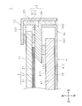
- FIG. 1 is a cross-sectional view schematically showing a configuration in the vicinity of the upper side portion of the optical sheet group 2 in the display device 1 according to Embodiment 1 of the present invention.
- 2 and 3 are cross-sectional views schematically showing configurations near the lower side and the left side of the optical sheet group 2 in the display device 1.
- FIG. 4 is a front view schematically showing a clamping / non-clamping range of the optical sheet group 2 included in the display device 1.
- a hatched portion in FIG. 4 indicates a range where the optical sheet group 2 is sandwiched.
- the display device 1 according to the present embodiment is configured as, for example, a television receiver, an electronic signboard, or a monitor for a personal computer.
- the display device 1 includes a display panel 11, a bezel 12, an optical sheet group 2, a P chassis (support portion) 3, a light source device 4, heat sinks and cabinets (not shown), and the like.
- the heat sink is for releasing heat generated in the display device 1 to the outside.
- the cabinet accommodates the display panel 11, the bezel 12, the optical sheet group 2, the P chassis 3, the light source device 4, the heat sink, and the like with the display area of the display panel 11 exposed.
- the display panel 11 is a liquid crystal display panel.
- the display panel 11 has a rectangular shape and is arranged in a vertical posture.
- the display panel 11 includes a rectangular display area and a rectangular frame-shaped frame area surrounding the display area.
- the display panel 11 uses a front glass substrate and a back glass substrate. Liquid crystal is sealed between the two glass substrates. The transmittance of the display panel 11 changes according to the voltage applied to the liquid crystal of the display panel 11.
- the bezel 12 is a frame-shaped support member for supporting the display panel 11 from the front side.
- the bezel 12 includes a rectangular frame-shaped front surface portion 121 in a vertical posture, and a front and rear rectangular tube-shaped side surface portion 122 protruding rearward from the outer peripheral edge portion of the front surface portion 121.
- the front part 121 covers the frame area of the display panel 11 from the front side.
- a rectangular frame-shaped buffer member 131 is disposed between the front surface portion 121 and the frame region of the display panel 11. The display area of the display panel 11 is exposed through the opening of the front surface part 121.
- the optical sheet group 2 forms a rectangular laminated body in which a plurality of rectangular optical sheets 21, 21,.
- the optical sheet group 2 is arranged in a vertical posture parallel to the rear surface of the display panel 11 and covers the display area of the display panel 11 from the back side.
- Each optical sheet 21 constituting the optical sheet group 2 has a light diffusing function or a light collecting function.
- the P chassis 3 is a frame-like support member for supporting the display panel 11 and the optical sheet group 2 from the back side, and has a non-light-transmitting property (such as a light shielding property or a light reflecting property).
- the P chassis 3 is disposed on the back side of the front surface portion 121 of the bezel 12 and on the inner side of the side surface portion 122.
- the P chassis 3 has a rectangular cylindrical base 31 in the front-rear direction, horizontal support pieces 32 and 32 and vertical support pieces 33 and 33 in each vertical posture.
- the base portion 31 is covered with the side surface portion 122 of the bezel 12.
- the lateral support pieces 32, 32 and the vertical support pieces 33, 33 protrude inward. More specifically, lateral support pieces 32 and 32 protrude downward (and upward) on the upper surface portion 311 (and the lower surface portion 312) of the base portion 31, and the side surface portions 313 and 313 (see FIG. 3) of the base portion 31.
- Vertical support pieces 33, 33 are provided so as to project sideways on the left side 313. The front side of the projecting position of the horizontal support pieces 32 and 32 and the vertical support pieces 33 and 33 in the base 31 covers the peripheral edge of the display panel 11.
- the horizontal support pieces 32 and 32 are for supporting the upper side and the lower side, which are the horizontal sides of the display panel 11. Between the horizontal support pieces 32 and 32 and the frame regions of the upper side and the lower side of the display panel 11, horizontal bar-shaped buffer members 132 and 132 are arranged. The upper side and the lower side of the display panel 11 are sandwiched between the front surface part 121 of the bezel 12 and the lateral support pieces 32, 32 of the P chassis 3 via buffer members 131, 132, 132.
- each buffer member 132 is longer than the thickness of the optical sheet group 2 even when compressed by clamping.
- the upper side and lower side of the optical sheet group 2 are loosely inserted into the gaps S1 and S1.
- the upper and lower ends of the optical sheet group 2 and the buffer members 132 and 132 are spaced apart by an appropriate length.
- the vertical support pieces 33 and 33 support the left side and right side which are the vertical sides of the display panel 11, and support the left side and right side of the optical sheet group 2.
- the left and right sides of the display panel 11 are interposed between the front surface 121 of the bezel 12 and the vertical support pieces 33 and 33 of the P chassis 3 via the buffer member 131 and the left and right sides of the optical sheet group 2. It is pinched. In other words, the left and right sides of the optical sheet group 2 are sandwiched between the left and right sides of the display panel 11 and the vertical support pieces 33 and 33 of the P chassis 3.
- a part of the peripheral edge (left side and right side) of the optical sheet group 2 is fixed by sandwiching the display panel 11 and the P chassis 3.
- the remaining part (upper side part and lower side part) of the peripheral part of the optical sheet group 2 is not fixed by clamping the display panel 11 and the P chassis 3.
- the opposing portions of the two opposing sides of the optical sheet group 2 are sandwiched, and the other two opposing sides (at least the lower side) are not sandwiched.
- One opposed two sides sandwiched are two vertical sides.
- the light source device 4 of the present embodiment includes a light guide plate 41, a reflection sheet 42, light sources 43 and 43, and a BL chassis 44.
- the light guide plate 41 has a rectangular plate shape.
- the light guide plate 41 is made of, for example, acrylic resin.
- the light incident on the inside of the light guide plate 41 is emitted from the front surface 411 of the light guide plate 41 (that is, the light guide plate 41 emits surface light).
- the rear surface 412 of the light guide plate 41 is provided with a plurality of reflecting portions (not shown).
- the light incident on the reflecting portion is reflected toward the front surface 411 side.
- the peripheral edge of the light guide plate 41 is disposed opposite to the horizontal support pieces 32 and 32 and the vertical support pieces 33 and 33 of the P chassis 3.
- a rectangular frame-shaped buffer member 133 having a light shielding property is disposed.
- the reflection sheet 42 has a rectangular shape.
- the reflection sheet 42 covers the rear surface 412 of the light guide plate 41.
- Each light source 43 includes a plurality of LEDs 431, 431,... And an LED substrate 432.
- the LED substrate 432 has a rectangular shape with a horizontal posture that is long in the left-right direction.
- the LEDs 431, 431,... Provided in the upper (or lower) light source 43 are equally mounted in a line in the left-right direction on the lower surface (or upper surface) of the LED substrate 432.
- the upper (or lower) light source 43 and the upper end surface (or lower end surface) of the light guide plate 41 are disposed to face each other with an appropriate distance therebetween.
- the light emitted from the light sources 43 and 43 does not enter the display panel 11 and the optical sheet group 2 as long as the light does not pass through the light guide plate 41.
- the BL chassis 44 has a rear surface portion 441 and a side surface portion 442.
- the BL chassis 44 supports each light source 43 via a heat sink (not shown).
- a light guide plate 41 and a reflection sheet 42 are sandwiched via a buffer member 133.
- the side surface portion 442 of the BL chassis 44 supports the rear side from the projecting position of the horizontal support pieces 32 and 32 and the vertical support pieces 33 and 33 in the base portion 31 of the P chassis 3 from the inside of the base portion 31.
- the light source device 4 may include a light source (for example, a fluorescent tube) supported by the BL chassis 44 so as to be positioned on the back side of the reflection sheet 42 instead of the light sources 43 and 43.
- the light source device 4 may include a diffusion plate instead of the light guide plate 41.
- the light emitted from the LEDs 431, 431,... Of the light sources 43, 43 is transmitted through the upper end surface or the lower end surface of the light guide plate 41 and enters the light guide plate 41.
- the light incident on the inside of the light guide plate 41 is reflected by the front surface 411, the rear surface 412, or the reflecting portion of the light guide plate 41, and eventually passes through the front surface 411 and is emitted to the outside of the light guide plate 41.
- a part of the light incident on the inside of the light guide plate 41 is transmitted through the rear surface 412 (that is, light leakage occurs). Light leakage from the rear surface 412 of the light guide plate 41 is reflected by the reflection sheet 42 and enters the light guide plate 41 again.
- the light transmitted through the front surface 411 of the light guide plate 41 and emitted to the outside passes through the optical sheet group 2 and then passes through the rear surface of the display panel 11 and enters the display panel 11. That is, the light emitted from the light source device 4 illuminates the display panel 11 from the back side through diffusion and condensing by the optical sheet group 2.
- the light incident on the display panel 11 passes through the display panel 11 or is blocked from passing through the display panel 11. As a result, an image is displayed in the display area of the display panel 11.
- the light guide plate 41 and the reflection sheet 42 of the present embodiment function as a light guide member that guides light emitted from the light sources 43 and 43 to the back side of the display panel 11.
- the assembly procedure of the display device 1 will be described.
- the worker arranges the reflection sheet 42, the light guide plate 41, and the buffer member 133 in this order on the front side of the rear surface portion 441 of the BL chassis 44. Further, the light sources 43 and 43 are attached to the BL chassis 44 together with the heat sink. Next, the worker attaches the P chassis 3 to the BL chassis 44. At this time, the rear end side of the base 31 of the P chassis 3 is supported on the side surface 442 of the BL chassis 44.
- the operator arranges the optical sheet group 2 on the front side of the horizontal support pieces 32 and 32 and the vertical support pieces 33 and 33 of the P chassis 3, and the buffer members 132 and 132 on the front side of the vertical support pieces 33 and 33. Place.
- the operator sandwiches the buffer members 132, 132 between the upper and lower sides of the display panel 11 and the lateral support pieces 32, 32 of the P chassis 3, and the left and right sides of the display panel 11 and the P
- the optical sheet group 2 is sandwiched between the vertical support pieces 33 and 33 of the chassis 3.
- the left and right sides of the optical sheet group 2 are sandwiched between the display panel 11 and the P chassis 3, and the upper and lower sides of the optical sheet group 2 are interposed between the display panel 11 and the P chassis 3.
- the gaps S1 and S1 formed are inserted with play.
- the operator places the buffer member 131 on the front side of the display panel 11 and then attaches the bezel 12 to the P chassis 3. At this time, the operator puts the buffer member 131 between the front surface portion 121 of the bezel 12 and the display panel 11 and attaches the side surface portion 122 of the bezel 12 to the base portion 31 of the P chassis 3.
- the optical sheet group 2 since the optical sheet group 2 does not need to be curvedly arranged unlike the optical sheet described in Patent Document 1, it is arranged flat so as to be parallel to the display panel 11. . This is because the left side portion and the right side portion of the optical sheet group 2 are sandwiched, and by applying appropriate tension between the left side portion and the right side portion of the optical sheet group 2, the posture of the optical sheet group 2 is flattened. This is because it can be maintained. That is, the optical sheet group 2 is unlikely to buckle.
- Arranging the optical sheet group 2 in parallel to the display panel 11 means that the light transmitted through the optical sheet group 2 easily enters the display panel 11 evenly. That is, since the display panel 11 is illuminated uniformly, the display quality of the display device 1 can be improved.
- the upper and lower sides of the optical sheet group 2 are not fixed by clamping. This means that the upward and downward elongation of the optical sheet group 2 is not inhibited during the thermal expansion of the optical sheet group 2. Moreover, since the upper side and the lower side of the optical sheet group 2 are closer to the light sources 43 and 43 than the left and right sides, heat generated by the light sources 43 and 43 is easily transmitted. That is, the upper side portion and the lower side portion of the optical sheet group 2 are more likely to thermally expand than the left side portion and the right side portion. In particular, the lower side portion of the optical sheet group 2 causes not only elongation due to thermal expansion but also elongation due to its own weight. From the above, the fact that the upper side portion and the lower side portion of the optical sheet group 2 are not clamped suitably suppresses unnecessary deformation of the optical sheet group 2 due to inhibition of the elongation of the optical sheet group 2. be able to.
- the light sources 43, 43 may be configured to be opposed to the left and right end faces of the light guide plate 41.
- the upper side part and the lower side part of the optical sheet group 2 may be fixed by clamping, and the left side part and the right side part of the optical sheet group 2 may not be fixed by clamping.
- the structure provided with only one of the light sources 43 and 43 may be sufficient.
- the far side from the light source 43, that is, the lower side (or upper side) of the optical sheet group 2 may be fixed by clamping.
- FIG. 5 and 6 are cross-sectional views schematically showing configurations near the upper right side and lower right side of the optical sheet group 2 in the display device 1 according to Embodiment 2 of the present invention.
- 5 and 6 correspond to FIG. 3 of the first embodiment.
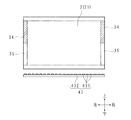
- FIG. 7 is a front view schematically showing a clamping / non-clamping range of the optical sheet group 2 included in the display device 1.
- FIG. 7 corresponds to FIG. 4 of the first embodiment, and a hatched portion in the figure indicates a range where the optical sheet group 2 is sandwiched.
- the display device 1 of the present embodiment has substantially the same configuration as the display device 1 of the first embodiment.
- differences from the first embodiment will be described, and other parts corresponding to those of the first embodiment are denoted by the same reference numerals and description thereof will be omitted.
- the display device 1 according to the present embodiment includes the lower light source 43 and does not include the upper light source 43.
- the P chassis 3 provided in the display device 1 of the present embodiment has vertical support pieces 34 and 34 instead of the vertical support pieces 33 and 33 of the first embodiment.
- the configuration of the vertical support pieces 34 and 34 is substantially the same as that of the vertical support pieces 33 and 33. However, an L-shaped notch-shaped recess 35 is provided on the front side of the tip portion of the lower half of each vertical support piece 34. That is, the configuration of the upper half of the vertical support pieces 34, 34 is the same as that of the vertical support pieces 33, 33, but the configuration of the lower half of the vertical support pieces 34, 34 is provided in the vertical support pieces 33, 33 in the recess 35, 35 is provided. Gaps S2 and S2 are formed between the inner surfaces of the recesses 35 and 35 and the display panel 11. The length in the front-rear direction of each gap S ⁇ b> 2 (the length from the rear surface of the display panel 11 to the rear inner surface of the recess 35) is longer than the thickness of the optical sheet group 2.
- the upper half of the left and right sides of the optical sheet group 2 is sandwiched between the left and right sides of the display panel 11 and the vertical support pieces 34 and 34 of the P chassis 3.
- the lower half part of the left side part and right side part of the optical sheet group 2 are loosely inserted into the gaps S2 and S2.
- the left end (and right end) of the optical sheet group 2 and the left inner surface (and right inner surface) of the gap S2 on the left side (and right side) are spaced apart by an appropriate length.
- the optical sheet group 2 is interposed between the display panel 11 and the vertical support pieces 33, 33, no buffer member is provided between them.
- the vertical bar-shaped buffer members 134 and 134 are disposed between the display panel 11 and the vertical support pieces 34 and 34 other than the tip portions. The thicknesses of the buffer members 134 and 134 that are sandwiched between the display panel 11 and the vertical support pieces 34 and 34 and are compressed are approximately the same as the thickness of the optical sheet group 2.
- the left side portion and the right side portion of the optical sheet group 2 are fixed by clamping the portions far from the light source 43 (that is, the upper half).
- the portion close to the light source 43 that is, the lower half
- the heat generated by the light source 43 is easily transmitted, and the portion where the expansion due to the thermal expansion and the own weight is likely to occur is not fixed. Therefore, useless deformation of the optical sheet group 2 due to inhibition of the elongation of the optical sheet group 2 can be suitably suppressed.
- the heat generated by the light source 43 is difficult to be transmitted and at least a part of the optical sheet group 2 that is difficult to stretch due to thermal expansion and its own weight is fixed, unnecessary vibration of the optical sheet group 2 is fixed. Is suppressed, and damage to the display panel 11 due to unnecessary vibration of the optical sheet group 2 is suppressed.
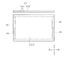
- FIG. FIG. 8 is a front view schematically showing a clamping / non-clamping range of the optical sheet group 2 provided in the display device 1 according to Embodiment 3 of the present invention.
- FIG. 8 corresponds to FIG. 7 of the second embodiment, and a hatched portion in the figure indicates a range where the optical sheet group 2 is sandwiched.
- the display device 1 of the present embodiment has substantially the same configuration as the display device 1 of the first and second embodiments.
- differences from the first and second embodiments will be described, and other parts corresponding to those of the second embodiment are denoted by the same reference numerals and description thereof will be omitted.
- the display device 1 of the present embodiment includes the upper light source 43 in the first embodiment, and does not include the lower light source 43.
- the P chassis 3 provided in the display device 1 of the present embodiment has vertical support pieces 34 and 34 that are substantially the same as the vertical support pieces 34 and 34 of the second embodiment.
- the vertical support pieces 34, 34 of the present embodiment are provided with recesses 36, 36 instead of the recesses 35, 35 of the second embodiment.
- Each recess 36 is provided in an L-shaped notch on the front side of the tip portion of the upper half of the vertical support piece 34. That is, the configuration of the lower half of the vertical support pieces 34, 34 is the same as that of the vertical support pieces 33, 33 of the first embodiment, but the configuration of the upper half of the vertical support pieces 34, 34 is the vertical support piece 33, 34.
- the configuration is such that recesses 36 and 36 similar to the recesses 35 and 35 of 33 are provided.
- a space similar to the gaps S2 and S2 of the second embodiment is formed between the inner surfaces of the recesses 36 and 36 and the display panel 11.
- the lower half of the left and right sides of the optical sheet group 2 are sandwiched between the left and right sides of the display panel 11 and the vertical support pieces 34 and 34 of the P chassis 3.
- the upper half part of the left side part and the right side part of the optical sheet group 2 is loosely inserted into the gap between the inner surface of the recesses 36 and 36 and the display panel 11.
- the left side portion and the right side portion of the optical sheet group 2 are fixed by clamping the portions far from the light source 43 (that is, the lower half).
- the portions near the light source 43 (that is, the upper half) on the left side and the right side of the optical sheet group 2 are not fixed by clamping.
- the heat generated by the light source 43 is easily transmitted, and the portion where the elongation due to thermal expansion is likely to occur is not fixed. Unnecessary deformation of the group 2 can be preferably suppressed.
- the heat generated by the light source 43 is difficult to transmit and at least part of the portion where elongation due to thermal expansion is difficult to occur is fixed, unnecessary vibration of the optical sheet group 2 is suppressed, Damage to the display panel 11 caused by unnecessary vibration of the optical sheet group 2 is suppressed.
- the display device 1 may include components that are not disclosed in the first to third embodiments.
- the constituent elements (technical features) disclosed in each embodiment can be combined with each other, and a new technical feature can be formed by the combination.
Landscapes
- Physics & Mathematics (AREA)
- Nonlinear Science (AREA)
- General Physics & Mathematics (AREA)
- Optics & Photonics (AREA)
- Mathematical Physics (AREA)
- Chemical & Material Sciences (AREA)
- Crystallography & Structural Chemistry (AREA)
- Liquid Crystal (AREA)
- Planar Illumination Modules (AREA)
Abstract
Description
以下では、液晶表示パネルが縦姿勢で配されている場合について説明する。
光源装置は、蛍光管又はLED等を用いてなる光源と、光源が発した光を表示パネルの背面側へ導く導光板又は拡散板等の導光部材と、光源及び導光部材を収容しているバックライトシャーシ(以下、BLシャーシという)とを有している。
光学シート群の周縁部は、液晶表示パネルとPシャーシとの間、又はPシャーシとBLシャーシとの間に配されている。光学シート群を構成する各光学シートは、一般に、液晶表示パネルに平行である。
特許文献1に記載の光学シートは、横方向中央部が液晶表示パネルから離隔するよう湾曲している。湾曲した光学シートは平坦な光学シートよりも座屈荷重が大きいので、自重による光学シートの座屈が抑制される。
一方、光学シートの周縁部の残部には、表示パネルと支持部との挟持による固定が為されていない。故に、光学シートの熱膨張は阻害されない。つまり、熱膨張に起因する光学シートの無用な変形が抑制される。
また、光学シートの周縁部における適宜の部分を挟持すれば、光学シートを湾曲配置する必要はない。
光学シートに対し、挟持されている部分の対向方向に張力を与えた場合、光学シートの姿勢を平坦状に保ち易い。
一の対向2辺部の全部が挟持されている場合、矩形状の光学シートにおける他の対向2辺部の少なくとも一部は挟持されていない。
光学シートの他の対向2辺部における少なくとも下辺部には、表示パネルと支持部との挟持による固定が為されていない。従って、光学シートの熱膨張及び自重による光学シートの伸びは阻害されない。つまり、熱膨張及び自重に起因する光学シートの無用な変形が抑制される。
光源から遠い部分に比べて、光源に近い部分には、光源が発した熱が伝達し易い。故に、光学シートの光源に近い部分は、光源から遠い部分に比べて熱膨張し易い。つまり、光学シートの熱膨張し易い部分が固定されていないので、熱膨張に起因する光学シートの無用な変形が更に抑制される。
しかも、このために光学シートを湾曲配置する必要がないので、光学シートを平坦に配置することができる。故に、液晶表示装置の組立性及び表示品位を向上させることができる。
図1は、本発明の実施の形態1に係る表示装置1における光学シート群2の上辺部近傍の構成を略示する断面図である。
図2及び図3は、表示装置1における光学シート群2の下辺部近傍及び左辺部近傍の構成を略示する断面図である。
図4は、表示装置1が備える光学シート群2の挟持/非挟持範囲を略示する正面図である。図4中のハッチング部分は光学シート群2が挟持されている範囲を示している。
本実施の形態の表示装置1は、例えばテレビジョン受信機、電子看板、又は、パーソナルコンピュータ用のモニタ等として構成されている。
表示装置1は、表示パネル11、ベゼル12、光学シート群2、Pシャーシ(支持部)3、及び光源装置4と、各不図示のヒートシンク及びキャビネット等とを備えている。
ヒートシンクは、表示装置1にて発生した熱を外部へ放出するためのものである。
キャビネットは、表示パネル11、ベゼル12、光学シート群2、Pシャーシ3、光源装置4、及びヒートシンク等を、表示パネル11の表示領域を露出させた状態で収容する。
前面部121は、表示パネル11の額縁領域を正面側から覆っている。前面部121と表示パネル11の額縁領域との間には、矩形枠状の緩衝部材131が配されている。前面部121の開口を通して表示パネル11の表示領域が露出している。
Pシャーシ3は、前後方向の矩形筒状の基部31と、各縦姿勢の横支持片32,32及び縦支持片33,33とを有する。
光学シート群2の上辺部及び下辺部は、空隙S1,S1に遊挿されている。光学シート群2の上端及び下端と緩衝部材132,132とは適長離隔配置されている。
換言すれば、光学シート群2の左辺部及び右辺部は、表示パネル11の左辺部及び右辺部とPシャーシ3の縦支持片33,33との間に挟持されている。
このように、本実施の形態では、光学シート群2の一の対向2辺部の対向する部分が挟持されており、他の対向2辺部(少なくとも下辺部)が挟持されていない。挟持されている一の対向2辺部は2個の縦辺部である。
導光板41の内部に入射した光は、導光板41の前面411から出射する(即ち、導光板41は面発光する)。このために、導光板41の後面412には、図示しない複数の反射部が設けられている。反射部に入射した光は、前面411側へ反射する。
導光板41の周縁部は、Pシャーシ3の横支持片32,32及び縦支持片33,33に対向配置されている。導光板41の周縁部とPシャーシ3の横支持片32,32及び縦支持片33,33との間には、遮光性を有する矩形枠状の緩衝部材133が配されている。
各光源43は、複数個のLED431,431,…とLED基板432とを備えている。
LED基板432は、左右方向に長い横姿勢の矩形状になしてある。
上方(又は下方)の光源43が備えるLED431,431,…は、LED基板432の下面(又は上面)にて左右方向に一列に等配実装してある。上方(又は下方)の光源43が備えるLED431,431,…と導光板41の上端面(又は下端面)とは、適長離隔して対向配置されている。
光源43,43が発した光は、導光板41を透過しない限り、表示パネル11及び光学シート群2に入射することはない。
BLシャーシ44は、図示しないヒートシンクを介して各光源43を支持している。BLシャーシ44の後面部441とPシャーシ3の横支持片32,32及び縦支持片33,33との間には、緩衝部材133を介して導光板41及び反射シート42が挟持されている。BLシャーシ44の側面部442は、Pシャーシ3の基部31における横支持片32,32及び縦支持片33,33の突設位置よりも後ろ側を基部31の内側から支持している。
表示パネル11の内部に入射した光は、表示パネル11を透過するか、又は、表示パネル11の通過を遮断される。この結果、表示パネル11の表示領域に映像が表示される。
本実施の形態の導光板41及び反射シート42は、光源43,43が発した光を表示パネル11の背面側へ導く導光部材として機能する。
作業者は、BLシャーシ44の後面部441の正面側に、反射シート42、導光板41、及び緩衝部材133をこの順に配置する。また、BLシャーシ44に、ヒートシンクと共に光源43,43を取り付ける。
次に、作業者は、BLシャーシ44にPシャーシ3を取り付ける。このとき、BLシャーシ44の側面部442にPシャーシ3の基部31の後端部側を支持させる。
次に、作業者は、表示パネル11の上辺部及び下辺部とPシャーシ3の横支持片32,32との間に緩衝部材132,132を挟み、表示パネル11の左辺部及び右辺部とPシャーシ3の縦支持片33,33との間に光学シート群2を挟む。
この結果、光学シート群2の左辺部及び右辺部は表示パネル11とPシャーシ3との間に挟持され、光学シート群2の上辺部及び下辺部は表示パネル11とPシャーシ3との間に形成されている空隙S1,S1に遊びを有して挿入される。
光学シート群2を表示パネル11に平行に配置することは、光学シート群2を透過した光が表示パネル11に均等に入射し易いことを意味する。つまり、表示パネル11が均等に照明されるので、表示装置1の表示品位を向上させることができる。
以上のことから、光学シート群2の上辺部及び下辺部が挟持されていないことは、光学シート群2の伸びが阻害されることに起因する光学シート群2の無用な変形を好適に抑制することができる。
また、光源43,43の一方のみが備えられている構成でもよい。上側(又は下側)の光源43のみが備えられている場合、光源43から遠い方、即ち、光学シート群2の下辺部(又は上辺部)は、挟持によって固定されていてもよい。
図5及び図6は、本発明の実施の形態2に係る表示装置1における光学シート群2の右辺上部近傍及び右辺下部近傍の構成を略示する断面図である。図5及び図6は実施の形態1の図3に対応する。
図7は、表示装置1が備える光学シート群2の挟持/非挟持範囲を略示する正面図である。図7は実施の形態1の図4に対応し、図中のハッチング部分は光学シート群2が挟持されている範囲を示している。
本実施の形態の表示装置1は、実施の形態1の表示装置1と略同様の構成である。以下では、実施の形態1との差異について説明し、その他、実施の形態1に対応する部分には同一符号を付してそれらの説明を省略する。
本実施の形態の表示装置1が備えるPシャーシ3は、実施の形態1の縦支持片33,33に替えて、縦支持片34,34を有している。
つまり、縦支持片34,34の上半分の構成は縦支持片33,33と同様の構成であるが、縦支持片34,34の下半分の構成は縦支持片33,33に凹部35,35が設けられたような構成である。
凹部35,35の内面と表示パネル11との間には、空隙S2,S2が形成される。各空隙S2の前後方向の長さ(表示パネル11の後面から凹部35の後内面までの長さ)は、光学シート群2の厚みよりも長い。
一方、光学シート群2の左辺部及び右辺部の下半部は、空隙S2,S2に遊挿されている。光学シート群2の左端(及び右端)と左側(及び右側)の空隙S2の左内面(及び右内面)とは適長離隔配置されている。
本実施の形態では、表示パネル11と縦支持片34,34の先端部分以外との間に、各縦棒状の緩衝部材134,134が配されている。表示パネル11と縦支持片34,34との間に挟持されて圧縮を受けている緩衝部材134,134夫々の厚みは、光学シート群2の厚みと同程度である。
一方、光学シート群2において、光源43が発した熱が伝達し難く、熱膨張及び自重に起因する伸びが生じ難い部分の少なくとも一部は固定されているので、光学シート群2の無用な振動が抑制され、光学シート群2の無用な振動に起因する表示パネル11の損傷が抑制される。
図8は、本発明の実施の形態3に係る表示装置1が備える光学シート群2の挟持/非挟持範囲を略示する正面図である。図8は実施の形態2の図7に対応し、図中のハッチング部分は光学シート群2が挟持されている範囲を示している。
本実施の形態の表示装置1は、実施の形態1,2の表示装置1と略同様の構成である。以下では、実施の形態1,2との差異について説明し、その他、実施の形態2に対応する部分には同一符号を付してそれらの説明を省略する。
本実施の形態の表示装置1が備えるPシャーシ3は実施の形態2の縦支持片34,34とほぼ同様の縦支持片34,34を有している。ただし、本実施の形態の縦支持片34,34には、実施の形態2の凹部35,35に替えて、凹部36,36が設けられている。
つまり、縦支持片34,34の下半分の構成は実施の形態1の縦支持片33,33と同様の構成であるが、縦支持片34,34の上半分の構成は縦支持片33,33の凹部35,35と同様の凹部36,36が設けられたような構成である。
凹部36,36の内面と表示パネル11との間には、実施の形態2の空隙S2,S2と同様の空間が形成される。
一方、光学シート群2の左辺部及び右辺部の上半部は、凹部36,36の内面と表示パネル11との間の空隙に遊挿されている。
一方、光学シート群2において、光源43が発した熱が伝達し難く、熱膨張による伸びが生じ難い部分の少なくとも一部は固定されているので、光学シート群2の無用な振動が抑制され、光学シート群2の無用な振動に起因する表示パネル11の損傷が抑制される。
また、本発明の効果がある限りにおいて、表示装置1に、実施の形態1~3に開示されていない構成要素が含まれていてもよい。
各実施の形態に開示されている構成要件(技術的特徴)はお互いに組み合わせ可能であり、組み合わせによって新しい技術的特徴を形成することができる。
11 表示パネル
2 光学シート群
21 光学シート
3 Pシャーシ(支持部)
4 光源装置
41 導光板(導光部材)
42 反射シート(導光部材)
43 光源
Claims (4)
- 表示パネルと、
該表示パネルを背面側から照明する光源装置と、
前記表示パネル及び光源装置の間に配されている光学シートと、
該光学シートを支持するための支持部と
を備える表示装置において、
前記光学シートの周縁部の一部は前記表示パネルと前記支持部とに挟持されており、
前記光学シートの周縁部の残部は前記表示パネルと前記支持部とに挟持されていないことを特徴とする表示装置。 - 前記光学シートは矩形状をなし、
前記光学シートの一の対向2辺部の対向する部分が挟持されていることを特徴とする請求項1に記載の表示装置。 - 前記光学シートは縦姿勢に配されており、
前記一の対向2辺部は2個の縦辺部であり、
前記光学シートの少なくとも下辺部が前記表示パネルと前記支持部とに挟持されていないことを特徴とする請求項2に記載の表示装置。 - 前記光源装置は、光源と該光源が発した光を前記表示パネルの背面側へ導く導光部材とを有しており、
前記周縁部の前記光源から遠い部分の少なくとも一部は挟持されており、
前記周縁部の前記光源に近い部分は挟持されていないことを特徴とする請求項1乃至3の何れか一項に記載の表示装置。
Priority Applications (4)
| Application Number | Priority Date | Filing Date | Title |
|---|---|---|---|
| PCT/JP2014/067671 WO2016002027A1 (ja) | 2014-07-02 | 2014-07-02 | 表示装置 |
| CN201480078471.2A CN106461999B (zh) | 2014-07-02 | 2014-07-02 | 显示装置 |
| JP2016530745A JP6212215B2 (ja) | 2014-07-02 | 2014-07-02 | 表示装置 |
| US15/305,574 US9874682B2 (en) | 2014-07-02 | 2014-07-02 | Display apparatus |
Applications Claiming Priority (1)
| Application Number | Priority Date | Filing Date | Title |
|---|---|---|---|
| PCT/JP2014/067671 WO2016002027A1 (ja) | 2014-07-02 | 2014-07-02 | 表示装置 |
Publications (1)
| Publication Number | Publication Date |
|---|---|
| WO2016002027A1 true WO2016002027A1 (ja) | 2016-01-07 |
Family
ID=55018625
Family Applications (1)
| Application Number | Title | Priority Date | Filing Date |
|---|---|---|---|
| PCT/JP2014/067671 Ceased WO2016002027A1 (ja) | 2014-07-02 | 2014-07-02 | 表示装置 |
Country Status (4)
| Country | Link |
|---|---|
| US (1) | US9874682B2 (ja) |
| JP (1) | JP6212215B2 (ja) |
| CN (1) | CN106461999B (ja) |
| WO (1) | WO2016002027A1 (ja) |
Families Citing this family (4)
| Publication number | Priority date | Publication date | Assignee | Title |
|---|---|---|---|---|
| JP2018049192A (ja) * | 2016-09-23 | 2018-03-29 | 株式会社デンソー | 表示装置 |
| US10454607B2 (en) * | 2017-02-23 | 2019-10-22 | Corning Incorporated | Mode division multiplexing systems and methods using a rectangular-core optical fiber |
| KR102380884B1 (ko) * | 2017-09-11 | 2022-03-31 | 삼성전자주식회사 | 디스플레이 모듈 및 이를 갖는 디스플레이 장치 |
| CN110174800B (zh) * | 2019-05-27 | 2024-07-26 | 武汉华星光电技术有限公司 | 背光模组和液晶模组 |
Citations (2)
| Publication number | Priority date | Publication date | Assignee | Title |
|---|---|---|---|---|
| JP2007025484A (ja) * | 2005-07-20 | 2007-02-01 | Hitachi Displays Ltd | 液晶表示装置 |
| JP2014092699A (ja) * | 2012-11-05 | 2014-05-19 | Sharp Corp | 液晶表示装置 |
Family Cites Families (6)
| Publication number | Priority date | Publication date | Assignee | Title |
|---|---|---|---|---|
| CN1324366C (zh) * | 2003-05-07 | 2007-07-04 | 瀚宇彩晶股份有限公司 | 一种液晶显示器及其背光模块 |
| JP4707517B2 (ja) | 2005-09-26 | 2011-06-22 | シャープ株式会社 | 液晶表示装置 |
| ATE549658T1 (de) * | 2007-05-31 | 2012-03-15 | Sharp Kk | Anzeigevorrichtung und fernsehempfänger |
| KR101960373B1 (ko) * | 2012-03-29 | 2019-03-20 | 엘지디스플레이 주식회사 | 백라이트 어셈블리와 이를 이용한 액정 표시 장치 |
| WO2014069572A1 (ja) * | 2012-11-05 | 2014-05-08 | シャープ株式会社 | 液晶表示装置 |
| CN103759227B (zh) * | 2014-01-22 | 2016-03-30 | 深圳市华星光电技术有限公司 | 一种光学膜片的定位装置 |
-
2014
- 2014-07-02 US US15/305,574 patent/US9874682B2/en not_active Expired - Fee Related
- 2014-07-02 WO PCT/JP2014/067671 patent/WO2016002027A1/ja not_active Ceased
- 2014-07-02 JP JP2016530745A patent/JP6212215B2/ja not_active Expired - Fee Related
- 2014-07-02 CN CN201480078471.2A patent/CN106461999B/zh not_active Expired - Fee Related
Patent Citations (2)
| Publication number | Priority date | Publication date | Assignee | Title |
|---|---|---|---|---|
| JP2007025484A (ja) * | 2005-07-20 | 2007-02-01 | Hitachi Displays Ltd | 液晶表示装置 |
| JP2014092699A (ja) * | 2012-11-05 | 2014-05-19 | Sharp Corp | 液晶表示装置 |
Also Published As
| Publication number | Publication date |
|---|---|
| CN106461999A (zh) | 2017-02-22 |
| US9874682B2 (en) | 2018-01-23 |
| JP6212215B2 (ja) | 2017-10-11 |
| US20170045679A1 (en) | 2017-02-16 |
| JPWO2016002027A1 (ja) | 2017-04-27 |
| CN106461999B (zh) | 2019-07-23 |
Similar Documents
| Publication | Publication Date | Title |
|---|---|---|
| CN106233194B (zh) | 显示装置 | |
| JP6212215B2 (ja) | 表示装置 | |
| JP6441488B2 (ja) | 表示装置 | |
| JP6284641B2 (ja) | 光源装置及び表示装置 | |
| US9507078B2 (en) | Black light module with mount and displaying apparatus therewith | |
| US20150277182A1 (en) | Display device | |
| US10359669B2 (en) | Display apparatus with spacer and method of manufacture of display apparatus with spacer | |
| CN107003560B (zh) | 背光源装置和液晶显示装置 | |
| CN105593594A (zh) | 照明装置和显示装置 | |
| WO2015037404A1 (ja) | 表示装置 | |
| US10132989B2 (en) | Backlight module and display device | |
| WO2015079485A1 (ja) | バックライト装置及び表示装置 | |
| WO2014208384A1 (ja) | 表示装置及びテレビ受像機 | |
| WO2010004822A1 (ja) | 照明装置、表示装置、テレビ受信装置 | |
| WO2014069572A1 (ja) | 液晶表示装置 | |
| US9829736B2 (en) | Display device | |
| US20190113675A1 (en) | Light source device and display device | |
| US9588283B2 (en) | Light source device and display apparatus | |
| JP6505121B2 (ja) | 光源装置及び表示装置 | |
| US9798188B2 (en) | Detecting accessories of a liquid crystal panel | |
| JP6329955B2 (ja) | 照明装置及び表示装置 | |
| US10031278B2 (en) | Light source device and display device | |
| JP2014021295A (ja) | 液晶表示装置 | |
| CN100462813C (zh) | 背光模块及其液晶显示器装置 | |
| KR101234463B1 (ko) | 백라이트 어셈블리 및 이를 구비한 액정표시장치 |
Legal Events
| Date | Code | Title | Description |
|---|---|---|---|
| 121 | Ep: the epo has been informed by wipo that ep was designated in this application |
Ref document number: 14896371 Country of ref document: EP Kind code of ref document: A1 |
|
| ENP | Entry into the national phase |
Ref document number: 2016530745 Country of ref document: JP Kind code of ref document: A |
|
| WWE | Wipo information: entry into national phase |
Ref document number: 15305574 Country of ref document: US |
|
| NENP | Non-entry into the national phase |
Ref country code: DE |
|
| 122 | Ep: pct application non-entry in european phase |
Ref document number: 14896371 Country of ref document: EP Kind code of ref document: A1 |