WO2015198533A1 - 樹脂付リードフレーム基板及びその製造方法 - Google Patents
樹脂付リードフレーム基板及びその製造方法 Download PDFInfo
- Publication number
- WO2015198533A1 WO2015198533A1 PCT/JP2015/002757 JP2015002757W WO2015198533A1 WO 2015198533 A1 WO2015198533 A1 WO 2015198533A1 JP 2015002757 W JP2015002757 W JP 2015002757W WO 2015198533 A1 WO2015198533 A1 WO 2015198533A1
- Authority
- WO
- WIPO (PCT)
- Prior art keywords
- resin
- lead frame
- metal
- insulating resin
- substrate
- Prior art date
- Legal status (The legal status is an assumption and is not a legal conclusion. Google has not performed a legal analysis and makes no representation as to the accuracy of the status listed.)
- Ceased
Links
Images


Classifications
-
- H—ELECTRICITY
- H10—SEMICONDUCTOR DEVICES; ELECTRIC SOLID-STATE DEVICES NOT OTHERWISE PROVIDED FOR
- H10W—GENERIC PACKAGES, INTERCONNECTIONS, CONNECTORS OR OTHER CONSTRUCTIONAL DETAILS OF DEVICES COVERED BY CLASS H10
- H10W72/00—Interconnections or connectors in packages
-
- H—ELECTRICITY
- H10—SEMICONDUCTOR DEVICES; ELECTRIC SOLID-STATE DEVICES NOT OTHERWISE PROVIDED FOR
- H10W—GENERIC PACKAGES, INTERCONNECTIONS, CONNECTORS OR OTHER CONSTRUCTIONAL DETAILS OF DEVICES COVERED BY CLASS H10
- H10W72/00—Interconnections or connectors in packages
- H10W72/50—Bond wires
- H10W72/551—Materials of bond wires
- H10W72/552—Materials of bond wires comprising metals or metalloids, e.g. silver
- H10W72/5522—Materials of bond wires comprising metals or metalloids, e.g. silver comprising gold [Au]
-
- H—ELECTRICITY
- H10—SEMICONDUCTOR DEVICES; ELECTRIC SOLID-STATE DEVICES NOT OTHERWISE PROVIDED FOR
- H10W—GENERIC PACKAGES, INTERCONNECTIONS, CONNECTORS OR OTHER CONSTRUCTIONAL DETAILS OF DEVICES COVERED BY CLASS H10
- H10W74/00—Encapsulations, e.g. protective coatings
-
- H—ELECTRICITY
- H10—SEMICONDUCTOR DEVICES; ELECTRIC SOLID-STATE DEVICES NOT OTHERWISE PROVIDED FOR
- H10W—GENERIC PACKAGES, INTERCONNECTIONS, CONNECTORS OR OTHER CONSTRUCTIONAL DETAILS OF DEVICES COVERED BY CLASS H10
- H10W90/00—Package configurations
- H10W90/701—Package configurations characterised by the relative positions of pads or connectors relative to package parts
- H10W90/751—Package configurations characterised by the relative positions of pads or connectors relative to package parts of bond wires
- H10W90/756—Package configurations characterised by the relative positions of pads or connectors relative to package parts of bond wires between a chip and a stacked lead frame, conducting package substrate or heat sink
Definitions
- the present invention relates to a lead frame substrate with resin and a method for manufacturing the same.
- an intermediary board called an interposer (semiconductor element mounting board) may be used.
- the interposer includes, for example, a lead frame type substrate formed by molding an insulating resin, that is, a lead frame substrate with resin (see Patent Document 1).
- solder balls may be disposed on the connection pads provided on the back surface of the lead frame substrate with resin, and solder bumps may be formed through a reflow process.
- the connection pad and the resin around it are on the same plane, the solder ball is likely to drop off, and the possibility of impairing connection reliability may increase.
- the resin-equipped lead frame substrate according to the related art has a problem that connection reliability between the resin-equipped lead frame substrate and the solder ball may be lowered.
- the present invention is intended to solve the above-described problems, and is capable of improving the connection reliability between a resin-equipped leadframe substrate and solder (solder balls), and a method for manufacturing the same. The purpose is to provide.
- a wiring pattern portion formed by removing a metal from a part of at least one surface of a metal base so that the plate thickness of the metal base is reduced.
- an insulating resin portion formed by substituting the insulating resin for the portion from which the metal is removed, and the height of the insulating resin portion is 3 ⁇ m or more higher than the height of the wiring pattern portion This is a resin-attached lead frame substrate.
- the height of the connection pad part which is a part of the wiring pattern part is made lower than the surrounding insulating resin part, or The height of the connection pad portion can be adjusted to be higher than that of the surrounding insulating resin portion by plating. Therefore, according to one embodiment of the present invention, it is possible to provide a resin-attached lead frame substrate and a method for manufacturing the same that can improve the connection reliability with solder.
- FIG. 1 It is sectional drawing which shows the structure of the lead frame board
- FIG. 3 is a cross-sectional view showing a positional relationship of plating layers provided in the resin-attached lead frame substrate according to Example 1. It is sectional drawing which shows the structure of a solder bump vicinity. 6 is a cross-sectional view showing a positional relationship of plating layers provided in a lead frame substrate with resin according to Comparative Example 1.
- the lead frame substrate with resin RFB includes a metal substrate 1, leads 4, electrode pads 5, a front surface die pad 7, a back surface die pad 8, an insulating resin portion 9, and a plating layer 10.
- FIG. 1 is a cross-sectional view of the resin-attached lead frame substrate RFB according to this embodiment.
- the metal substrate 1 is formed using copper etc., for example.
- the lead 4 is formed on one surface (main surface) of the metal base 1 using, for example, a photosensitive resist or a dry film.
- the main surface is also simply referred to as “surface”.
- the electrode pad 5 is formed on the other surface (the surface opposite to the main surface) of the metal substrate 1 by using, for example, a photosensitive resist or a dry film.
- the surface opposite to the main surface is also simply referred to as “back surface”.
- the surface die pad 7 is formed on the surface of the metal substrate 1 using, for example, a photosensitive resist or a dry film.
- the back surface die pad 8 is formed on the back surface of the metal substrate 1 using, for example, a photosensitive resist or a dry film.
- the insulating resin portion 9 is formed using, for example, a transfer mold method described later.
- the plating layer 10 is formed on the surface of the lead 4, the electrode pad 5, the front surface die pad 7 and the back surface die pad 8 (surface opposite to the surface facing the metal substrate 1).
- the resin-attached lead frame substrate RFB is formed to include a plurality of pieces (9 pieces in the example shown in the drawings).
- FIG. 2 is a plan view showing the surface of nine adjacent pieces of the resin-attached lead frame substrate RFB according to this embodiment.
- FIG. 3 is a plan view showing the back surface of nine adjacent pieces of the resin-attached lead frame substrate RFB according to this embodiment.
- a pattern of the tie bar 20 is formed between adjacent pieces using, for example, a photosensitive resist or a dry film.
- FIG. 4 is a plan view showing one piece constituting the surface of the resin-attached lead frame substrate RFB according to the present embodiment.
- the pattern of the back surface die pad 8 and the pattern of the electrode pad 5 are formed on one piece constituting the back surface of the resin-attached lead frame substrate RFB using, for example, a photosensitive resist or a dry film.
- FIG. 5 is a plan view showing one piece constituting the back surface of the resin-attached lead frame substrate RFB according to the present embodiment.
- the pattern position of the back surface die pad 8 formed on the back surface of the lead frame substrate with resin RFB is a part of the back side of the position of the lead 4 on the surface of the lead frame substrate with resin RFB, and in many cases, the position of one end of the lead The back side.
- the pattern of the surface die pad 7 is located at the center of the metal base 1, and the pattern of the leads 4 extends radially outward from the vicinity thereof.
- the pattern of the back surface die pad 8 is formed on the back side of the outermost position of the pattern of the leads 4.
- the method of manufacturing a lead frame substrate with resin includes a wiring pattern forming step and an insulating resin portion forming step, and the insulating resin portion forming step includes an insulating resin filling step, a molten insulating resin solidifying step, and a pattern removing step. Including.
- the wiring pattern forming step first, a part of the metal plate is removed by etching or the like. Specifically, with respect to the metal substrate 1 shown in FIG. 7 (a), as shown in FIG.
- the photosensitive resist 2 is applied to both surfaces of the metal substrate 1 by, for example, a roll coater. After coating, pre-bake. Next, pattern exposure is performed from both sides via a pattern exposure photomask having a desired pattern, which will be described later, and then development processing is performed. Finally, washing with water and post baking are performed to form a resist pattern 3 as shown in FIG.
- FIG. 7 is a cross-sectional view showing a wiring pattern forming step.
- etching is performed from both surfaces of the metal base 1 using, for example, a ferric chloride solution or the like, as shown in FIG.
- the resist removal after the etching process is not performed, and the process proceeds to the insulating resin portion forming process which is the next process while leaving the resist pattern 3 left.
- a surface die pad 7, leads 4, suspension leads 19 (not shown), and tie bars 20 are formed on the surface of the metal substrate 1.
- a back surface die pad 8 and an electrode pad 5 are formed on the back surface.
- the wiring pattern portion is also referred to as a “wiring pattern portion”.
- the metal removal portion of the metal plate (metal substrate 1) formed in the wiring pattern forming step is filled with insulating resin to form the insulating resin portion 9.
- the most suitable method for forming the insulating resin portion 9 is a so-called transfer molding method. The steps of this transfer mold method will be briefly described below. First, as shown in FIG. 8, the metal plate (metal substrate 1) formed in the wiring pattern forming step is sandwiched between the upper mold 21 and the lower mold 22 and clamped. Thereafter, the solid resin is poured into the mold in a state of being melted by heating (melted insulating resin 23), and the metal removal portion of the metal plate (metal substrate 1) and the inner walls of the upper mold 21 and the lower mold 22 are formed. Fill the cavity to make (insulating resin filling process). Finally, the resin poured into the mold is solidified (molten insulating resin solidification step).
- the transfer mold method when the metal mold (upper metal mold 21 and lower metal mold 22) and the metal plate (metal base material 1) are in close contact with each other, a resin (molten insulating resin 23) is interposed therebetween. Ideally it should not penetrate. In practice, however, the insulating resin 23 melted only slightly from a slight gap between the mold and the metal plate usually enters a burr. In general, the molten insulating resin 23 is filled and solidified and then removed by a physical or chemical method. As a result, the surface of the lead frame substrate with resin and the back surface of the resin-made lead frame substrate have the same height as the surface of the metal plate (metal substrate 1) and the surface of the insulating resin, thereby forming the same plane.
- a metal plate (metal plate formed in the wiring pattern forming step: lead frame) after removing a predetermined portion of metal is molded from the thickness direction.
- a molten insulating resin is injected into a cavity formed between the upper mold 21 and the lower mold 22 to be clamped and formed in the above-described mold clamping state, and then solidified.
- the insulating resin portion 9 is formed on the portion of the metal substrate 1 where the metal is removed while leaving the resist pattern 3. Is replaced by In the pattern removing step, after the molten insulating resin injected into the cavity is solidified with the resist pattern 3 left, the resist pattern 3 is removed as shown in FIG.
- the lead frame with resin according to the present embodiment is formed.
- Example 1 As a manufacturing method of the leadframe substrate with resin according to the first embodiment, a manufacturing method of an LGA (Land Grid Array) type leadframe substrate will be described as an example.
- LGA Large Grid Array
- Each LGA produced in Example 1 has a size of 10 mm square, and has 64 pins of external connection terminals in an array shape in plan view.
- the substrate was multifaceted and cut and cut after the following manufacturing steps to obtain individual LGA type lead frames with resin (for example, see FIG. 7). In the figure, the number of pins is omitted and the numbers are reduced.
- a metal substrate 1 having a long strip shape having a width of 90 mm and a thickness of 200 ⁇ m was prepared (see FIG. 7A).
- a photosensitive resist 2 manufactured by Tokyo Ohka Co., Ltd., OFPR4000 was coated on both surfaces of the metal substrate 1 so as to have a thickness of 10 ⁇ m with a roll coater, and then prebaked at 90 ° C. (Refer FIG.7 (b)).
- pattern exposure was performed from both sides of the metal substrate 1 through a photomask for pattern exposure having a desired pattern (described later), and then development processing was performed with a 1% sodium hydroxide solution.
- a resist pattern 3 for forming a surface die pad 7 for mounting a semiconductor element and a wiring pattern are formed on one surface side of the metal substrate 1 (that is, the surface on which the semiconductor element is mounted).
- a resist pattern 3 was formed.
- the resist pattern 3 for forming the electrode pad 5 and the semiconductor to be mounted are formed on the other surface of the metal substrate 1 (that is, the back surface that is the surface opposite to the surface on which the semiconductor element is mounted).
- a resist pattern 3 for forming a backside die pad 8 for releasing heat from the element was formed.
- the resist pattern 3 will be described in detail with reference to FIGS.
- a pattern of a surface die pad 7 for mounting a semiconductor element was disposed.
- the surface die pad 7 since the surface die pad 7 also plays a role of releasing heat generated by the semiconductor element to the outside, the surface die pad 7 basically passes through the metal substrate 1 and reaches the back surface.
- the size of the outer periphery is slightly changed to taper the cross section of the surface die pad 7 and increase the contact area with the insulating resin portion 9 to improve adhesion.
- the resist pattern 3 is formed as the back die pad 8 without changing the center position.
- the patterns of the suspension leads 19 extending radially are arranged in the directions of the nearest four corners of one piece of the substrate.
- the resist pattern 3 is not formed at a position corresponding to the suspension lead 19 on the back surface.
- the pattern of the suspension leads 19 is connected to the tie bar 20 at a position on the outer periphery of one piece of the substrate.
- the tie bar 20 has the same position as the outer periphery of one piece of the substrate.
- the thickness of the tie bar 20 is halfway in the thickness direction of the metal substrate 1, and the resist pattern 3 corresponding to the back surface is not formed.
- the resist pattern 3 of the leads 4 was arranged on the surface in a reverse radial manner in the direction of the surface die pad 7 in a state of being connected from the tie bar 20.
- the lead 4 extends in the direction of the surface die pad 7 but is not connected to the surface die pad 7.
- the thickness of the lead 4 was set smaller than the thickness of the metal substrate 1, and the resist pattern 3 of the lead 4 was not formed at the corresponding position on the back surface.
- the lead 4 arrange
- the resist pattern 3 of the electrode pad 5 is disposed at the end connected to the tie bar 20 among both ends of the lead 4.
- the thickness of the electrode pad 5 was the same as the thickness of the metal substrate 1.
- the resist pattern 3 of the lead 4 also serves as the electrode pad 5 (the back surface thereof).
- the resist pattern 3 was arranged in a rectangular shape with rounded corners. After the formation of the resist pattern 3, etching was performed from both surfaces of the metal substrate 1 using a ferric chloride solution (see FIG. 7D).
- the depth to be etched when etching was performed from one side of the metal substrate 1, conditions were set so that the thickness of the metal substrate 1 was 200 ⁇ m to 90 ⁇ m, and then both surfaces were etched simultaneously. At that time, the specific gravity of the ferric chloride solution was 1.38, and the temperature was 50 ° C. Further, the resist peeling after the etching was not performed, and the process proceeded to the insulating resin portion forming step by the next transfer molding method while leaving the resist pattern 3 left. By the etching process, the surface die pad 7, the lead 4, the suspension lead 19, and the tie bar 20 are formed on the surface of the metal substrate 1, and the back die pad 8 and the electrode pad 5 are formed on the back surface of the metal substrate 1. It was done.
- the metal substrate 1 was cut so as to fit in a predetermined position of the mold for filling the insulating resin by the transfer mold method. As a result of the cutting, the metal substrate 1 became a strip-shaped frame (lead frame) having a width of 90 mm and a length of 300 mm.
- the lead frame metal substrate 1
- the lead frame metal base 1
- the lower mold 22 is formed with a recess having the same depth as the thickness of the lead frame and substantially the same (slightly larger) in plan view, and a groove for introducing a resin connected to the recess.
- the upper mold 21 having a polished horizontal surface as a surface in contact with the lead frame is put on and the mold is clamped.
- a solid epoxy resin insulating resin
- the upper mold 21 was opened after the insulating resin was solidified, and the lead frame filled with the insulating resin was taken out from the lower mold 22. Since the insulating resin remaining in the flow path for guiding the insulating resin from the outside of the mold to the inside of the mold and the recess in the mold is solidified and adhered to the lead frame, Removed manually. Subsequently, post-baking was performed to completely solidify the insulating resin filled in the lead frame. As a post-bake condition, heating was performed in an oven at 150 ° C. for 2 hours. In the lead frame in this state, the insulating resin fills the metal removal portion of the lead frame in a substantially flush state, but slight exudation to the substrate surface in the mold is almost inevitable.
- the melted insulating resin 23 that has oozed out in the mold becomes a resin burr 24 and is very thin and adheres to each part of the resist pattern 3 on the lead frame.
- This resin burr 24 must be removed because it causes a defect in the connection after the subsequent plating process or the lead frame substrate with resin is completed and the semiconductor element is mounted. In Example 1, the removal was performed by peeling off the resist pattern 3.
- the pattern removal process was performed following the insulating resin filling process and post-baking.
- an alkaline solution 400 g of NaOH / 1 L as a main component
- a stripping solution heated to 95 ° C.
- the conveying speed is set so that the residence time is 3 minutes. Adjusted.
- the stripping solution not only strips the resist pattern 3 but also has an effect of promoting swelling of the epoxy resin on the resist pattern 3 as the resin burr 24.
- continuous high-pressure water washing with a water pressure of 10 MPa was performed for 1 minute on the inline device, and the resist pattern 3 was washed away together with the resin burr 24.
- each lead frame (lead frame with resin) according to Example 1 was formed.
- Example 1 an electroless nickel / palladium / gold plating forming method that does not require a supply electrode is employed.
- the exposed metal surface is subjected to acidic degreasing, soft etching, acid cleaning, palladium catalyst activation treatment, pre-dip, electroless nickel plating, electroless palladium plating, and electroless gold plating to form a plating layer 10 did.
- the thickness of each layer included in the plating layer 10 is 3 ⁇ m for nickel, 0.2 ⁇ m for palladium, and 0.03 ⁇ m for gold.
- the thickness of the plating layer 10 is the sum of the above layers. It was.
- the plating solution used is Enplate NI (made by Meltex), palladium is Paulobond EP (made by Rohm and Haas), and gold is Paulobond IG (made by Rohm and Haas).
- the metal portion of the lead frame with resin is lower than the surrounding insulating resin portion 9 by the thickness of the resist film. In this stage, it is in a state of being recessed from the surrounding insulating resin portion 9 by about 7 ⁇ m.
- a desired resin-attached lead frame substrate RFB was obtained by the procedure described above.
- FIG. 12 sectional drawing showing the positional relationship of the plating layer 10 with which the lead frame board
- Example 1 as a means for removing a predetermined metal portion of the lead frame with resin, a step of forming an insulating resin portion 9 using etching by forming a resist pattern in addition to the portion to be removed is further provided. This was performed with the resist pattern 3 left. With this manufacturing method, as shown in FIG. 11, the resin burr 24 generated in the transfer molding method runs on the resist film on the metal part, but the pattern is formed after filling and curing the insulating resin. In the removing step, the resist pattern 3 is removed.
- the insulating resin portion 9 is molded to have the same height as the surface of the resist film on the metal portion. For this reason, in the insulating resin part 9, after the resist is stripped, the height of the metal part is lower than that of the insulating resin part 9 by the thickness of the resist film.
- the thickness of the resist pattern 3 was 3 ⁇ m or more. This is because if the thickness of the resist pattern 3 is less than 3 ⁇ m, the resist pattern 3 does not play a role during etching.
- the generated resin burr 24 runs on the resist film.
- the resin-attached lead frame substrate RFB according to the first embodiment prevents plating defects due to burrs remaining. That is, with the method for manufacturing the leadframe substrate RFB with resin according to the first embodiment, it is possible to provide a simple and reliable method for removing the resin burr 24 in the manufacturing process of the leadframe substrate with resin RFB.
- Example 2 In Example 2, the metal portion exposed on the front surface and the reverse surface, which is the opposite surface, was plated on the sample of Example 1.
- the metal part was made higher than the upper surface of the insulating resin part 9.
- the connection area of the solder ball 6 and the connection pad is widened, and the connection strength and the shear strength are improved.
- the height relationship between the metal part and the insulating resin part 9 is opposite to the structure of the first embodiment, but the structural features required to obtain connection reliability are the pattern of the substrate and the substrate. It depends on the structure of the entire package, the mounting conditions of the elements, the usage environment of the package, and the like. For this reason, as described above, the metal part is made lower than the insulating resin part 9, and then the height of the metal part can be adjusted by the thickness of the plating layer 10 as necessary. Is effective.
- Comparative Example 1 In Comparative Example 1, the thickness of the resist film was set to 5 ⁇ m in forming the resist pattern 3 on the metal substrate 1. Further, the thickness of each layer included in the plating layer 10 is 5 ⁇ m for nickel, 0.2 ⁇ m for palladium, and 0.03 ⁇ m for gold. The total value was used. As a result, on the surface of the lead frame with resin, the upper surface of the metal part and the upper surface of the insulating resin part 9 were almost the same height. Otherwise, the resin-attached lead frame substrate RFB was obtained using the same method as in Example 1. In addition, in FIG. 14, sectional drawing showing the positional relationship of the plating layer 10 with which the lead frame board
- Comparative Example 2 In Comparative Example 2, the thickness of the resist film was set to 5 ⁇ m in forming the resist pattern 3 on the metal substrate 1. Further, the thickness of each layer included in the plating 10 is 8 ⁇ m for nickel, 0.2 ⁇ m for palladium, and 0.03 ⁇ m for gold, and the thickness of the plating layer 10 is the sum of the above layers. Value. As a result, the upper surface of the metal part slightly protruded from the upper surface of the insulating resin part 9 on the surface of the lead frame with resin. Otherwise, the resin-attached lead frame substrate RFB was obtained using the same method as in Example 1. In addition, in FIG. 15, sectional drawing showing the positional relationship of the plating layer 10 with which the lead frame board
- Comparative Example 3 In Comparative Example 3, the resist was peeled after the etching process of the metal substrate 1. The peeling conditions are the same as in Example 1. Then, resin filling by a transfer mold method was performed, and the subsequent resist peeling process was not performed. Otherwise, the resin-attached lead frame substrate RFB was obtained using the same method as in Example 1. In addition, in FIG. 16, sectional drawing showing the positional relationship of the plating layer 10 with which the lead frame board
- an evaluation element was mounted on the lead frame substrate with resin RFB of each example and each comparative example.
- the evaluation in this case relates to the connection between the lead frame substrate with resin RFB and the mother board by solder balls.
- the evaluation element mounted on the lead frame substrate with resin RFB has the same external shape and material as that of a normal element, and the internal wiring only connects terminals.
- the element for evaluation is mounted on the die pad of the lead frame substrate with resin RFB using a die attach film, and is further electrically connected to the substrate by wire bonding using a gold wire with a diameter of 25 ⁇ m. It was.
- the evaluation element was resin-sealed by a transfer mold method to obtain a semiconductor package.
- solder balls having a radius of 300 ⁇ m were placed thereon, and solder bumps were formed through a reflow furnace.
- the test for continuity after the secondary mounting was performed by examining between two points on the terminals of the motherboard, and by selecting these two points, the design was made so that continuity and breakage for any solder bump could be seen.
- initial evaluation it was confirmed that all the solder bumps were electrically connected, and only the samples judged to have no initial failure were put into TCT (temperature cycle test).
- TCT temperature cycle test
- the TCT conditions were 1000 cycles by switching between ⁇ 55 ° C. and 125 ° C. for 10 minutes each.
- the conduction of each bump was examined again.
- the sample was hardened with an epoxy resin, the cross section was polished, and the destruction and peeling of the solder were observed.
- Example 1 in which the metal part including the plating layer is lower than the surrounding insulating resin part 9, the solder balls can be reliably arranged. Moreover, in the evaluation of the samples that have been performed up to the secondary mounting, it is more reliable that the metal part including the plating layer protrudes from the surrounding insulating resin part 9 as in Comparative Example 2 or Comparative Example 3. Is high. This is because, as shown in FIG. 13, when the solder bumps are formed, they are in close contact with the side surfaces of the protruding metal part to increase the bonding area.
- Example 1 Even in Example 1, the number of defects is zero, but this is different from the above reason.
- the presence of the insulating resin wall around the electrode is based on the connection reliability in the current material configuration and substrate structure. This is because it worked to improve sex. If the material structure and the substrate structure are different, the relationship between the height of the metal part and the connection reliability may be different from this time, and the height of the metal part may be changed from the insulating resin part 9 before plating. It is preferable that the height be adjusted so that the height can be adjusted in the subsequent plating step depending on the situation.
- the resin-attached lead frame substrate and the manufacturing method thereof according to one aspect of the present invention can solve the problems to be solved by the present invention.
- Various kinds of memories, semiconductors such as CMOS, CPU, and FPGA manufactured by the wafer process have terminals for electrical connection.
- the pitch of the electrical connection terminals and the pitch of the connection parts on the printed circuit board side where the semiconductor elements are mounted differ by about 1 to 2 digits due to the difference in the construction method. Therefore, an intermediary substrate (semiconductor element mounting substrate) for pitch conversion called an interposer is used.
- FIG. 17 is a diagram schematically showing the structure of a QFN (Quad Flat Non-leaded) type lead frame as an example of an interposer.
- the semiconductor element 11 is fixed to a predetermined portion of the lead frame affixed to the holding material 14 made of polyimide tape with the fixing resin 16 or the fixing tape. .
- wire bonding is performed, and a plurality of chips (semiconductor elements 11) are collectively resin-molded by a transfer molding method.
- exterior processing is performed, and individual products are cut and cut into finished products.
- the QFN type lead frame is provided with a flat portion 12 on which the semiconductor element 11 is mounted at the center portion of a lead frame made of metal such as copper or aluminum, and has a pitch on the outer peripheral portion.
- a wide lead 4 (not shown) is provided.
- a bonding method using a metal wire 13 such as a gold wire is used for connection between the lead 4 and the electrical connection terminal of the semiconductor element 11.
- the holding member 14 shown in FIGS. 17A and 17B holds the lead frame, and as shown in FIG. 17C, an insulating resin (molding resin 17) is used. It is removed after molding.
- the interposer shown in FIG. 17 can be electrically connected only between the outer periphery of the semiconductor element and the outer periphery of the lead frame.
- the connection between the printed board and the interposer is performed by attaching a metal pin to the take-out electrode 15 of the extension part of the interposer.
- solder balls are arranged in an array (Ball Grid Array) on the external connection terminals on the outer peripheral portion. Since the connection pitch on the printed circuit board side is as wide as about 500 ⁇ m and the amount of solder is large, the Ball Grid Array is capable of stable and reliable connection. For semiconductor devices with a small area and a large number of terminals, it is difficult to change the pitch with an interposer with a single electrical path, so layers with electrical paths are laminated in two or three layers. ing.
- connection terminals of the semiconductor element are often formed in an array on the bottom surface of the semiconductor element.
- the external connection terminals on the interposer side are also arranged in the same array, and a flip chip connection method using minute solder balls is adopted for the connection between the interposer and the printed circuit board.
- the wiring in the interposer is drilled or drilled in the vertical direction from the upper part, and metal plating is performed in the hole, so that electrical conduction is made up and down.
- the pitch of the external connection terminals can be miniaturized to a range of 150 ⁇ m or more and 200 ⁇ m or less, so that the number of connection terminals can be increased, but the reliability and stability of bonding are lowered. For this reason, this type of interposer is not suitable for in-vehicle use or the like where high reliability is required.
- such an interposer has a ceramic base material for holding the lead frame part, or a P-BGA (Plastic Ball Grid Array), CSP (Chip Size Package), LGA (Land).
- P-BGA Physical Ball Grid Array
- CSP Chip Size Package
- LGA Land
- base materials such as organic ones such as (Grid Array) and the like, and they are properly used according to the purpose.
- the pitch of the terminal portion needs to be in the range of 80 ⁇ m to 100 ⁇ m.
- the lead frame which is also a conductive portion and supporting member, is formed by a so-called photoetching method, which is manufactured by etching a thin metal plate.
- the metal plate has a thickness of about 200 ⁇ m.
- the required minimum thickness of the metal plate is about 200 ⁇ m. In that case, it is preferable to perform etching from both sides of the metal plate.
- the holding material 14 made of polyimide tape that covers the back surface 18 of the lead frame (the surface opposite to the surface on which the semiconductor element 11 is mounted) is used when the back surface 18 of the lead frame serves as a connection surface with the printed circuit board. In order to prevent the molding resin 17 from wrapping around and adhering to the connection terminal surface on the back surface of the lead during molding, it is indispensable.
- the holding material 14 made of polyimide tape is unnecessary in the end, it is removed and discarded after molding. Therefore, the method of manufacturing the interposer by attaching the lead frame to the holding material 14 has a problem that it is costly.
- a lead frame type substrate that is formed by forming irregularities or through holes on both sides of a metal plate using pattern etching, half etching, etc., and molding an insulating resin on the formed portion.
- the substrate having this structure since the insulating resin has a function of supporting the wiring pattern, it is not necessary to attach a polyimide tape, and it is possible to realize cost reduction.
- connection reliability when mounting an element on an electronic board formed as described above, if the height of the metal part (wiring pattern) and the insulating resin part are aligned as in the prior art, from the viewpoint of connection reliability and the like. , Often undesired.
- solder balls are formed on the connection pads on the back surface of the lead frame substrate with resin and solder bumps are formed through a reflow process, if the connection pads and the insulating resin portion around them are on the same plane, the solder The ball is likely to fall off, and the possibility of impairing connection reliability increases.
- the lead frame substrate with resin according to the prior art has a problem that the connection reliability between the lead frame substrate with resin and the solder ball may be lowered.
- the resin-equipped lead frame substrate FRB has Insulation between the lead frame 25 including the wiring pattern portion (for example, the lead 4, the electrode pad 5, the front surface die pad 7, and the back surface die pad 8) formed by removing the metal so that the plate thickness is reduced, and the portion from which the metal is removed And an insulating resin portion 9 formed by substitution with resin.
- the height of the insulating resin portion 9 is 3 ⁇ m or more higher than the height of the wiring pattern portion.
- connection pad portion for example, the electrode pad 5, the front surface die pad 7, the back surface die pad 8 which is a part of the wiring pattern portion on the surface of the lead frame substrate with resin FRB is set to be around. It becomes possible to make it lower than the insulating resin part 9. For this reason, the resin-attached lead frame substrate FRB according to the present embodiment can improve the connection reliability with the solder.
- the manufacturing method of the lead frame substrate with resin removes the metal from a part of at least one surface of the metal base 1 so that the plate thickness of the metal base 1 decreases.
- a wiring pattern forming step for forming a predetermined wiring pattern, and an insulating resin portion 9 that is higher than the height of the wiring pattern portion on which the wiring pattern of the metal substrate 1 is formed is replaced with an insulating resin in the portion where the metal is removed.
- Insulating resin filling step for filling 23, and a molten insulating resin solidifying step for solidifying the insulating resin 23 filled in the insulating resin filling step With such a configuration, the height of the connection pad portion described above can be made lower than that of the surrounding insulating resin portion 9 on the surface of the lead frame substrate with resin FRB. For this reason, if it is the manufacturing method of the lead frame board
- the insulating resin portion forming step may include a pattern removing step of removing the resist pattern 3 after solidifying the insulating resin 23 filled in the cavity with the resist pattern 3 left.
- the resin burr 24 generated during the insulating resin portion forming step can be reliably removed together with the resist pattern 3 in the pattern removing step. For this reason, it is possible to prevent plating defects due to burrs remaining. Therefore, the method for manufacturing the resin-attached lead frame substrate RFB according to the present embodiment can provide a simple and reliable method for removing the resin burr 24 in the process of manufacturing the resin-attached lead frame substrate RFB.
- the thickness (film thickness) of the resist pattern 3 may be 3 ⁇ m or more.
- the resist pattern 3 can serve as a mask (function) in etching. If the thickness of the resist pattern 3 is less than 3 ⁇ m, it may not serve as a mask for the resist pattern 3 during etching.
- the height of the connection pad portion, which is a part of the wiring pattern portion can be made 3 ⁇ m or more lower than the surrounding insulating resin portion 9 on the surface of the lead frame substrate with resin FRB. It becomes. For this reason, if it is the manufacturing method of the lead frame board
- the manufacturing method of the lead frame substrate with resin according to the present embodiment may include a plating layer forming step of forming the plating layer 10 on the wiring pattern portion after the insulating resin portion forming step.
- a plating layer forming step of forming the plating layer 10 on the wiring pattern portion after the insulating resin portion forming step it is possible to adjust the height of the connection pad portion, which is a part of the wiring pattern portion, to be higher than that of the surrounding insulating resin portion 9 by plating.
- Even with such a method of manufacturing a resin-attached lead frame substrate FRB it is possible to provide a resin-attached lead frame substrate with improved connection reliability with solder.
- the present invention relates to a semiconductor substrate for mounting a semiconductor element, and can be used particularly for a lead frame type substrate and a manufacturing method thereof.
- SYMBOLS 1 Metal base material, 2 ... Photosensitive resist, 3 ... Resist pattern, 4 ... Lead, 5 ... Electrode pad, 6 ... Solder ball, 7 ... Front surface die pad, 8 ... Back surface die pad, 9 ... Insulating resin part, 10 ... Plating Layer 11, semiconductor element 12, flat portion 13, metal wire 14, holding material 15, take-out electrode 16, fixing resin, 17 resin for molding, 18 back surface of lead frame, 19, suspended lead 20 ... Tie bar, 21 ... Upper mold, 22 ... Lower mold, 23 ... Molten insulating resin, 24 ... Resin burr, 25 ... Lead frame, RFB ... Lead frame substrate with resin
Landscapes
- Lead Frames For Integrated Circuits (AREA)
- Encapsulation Of And Coatings For Semiconductor Or Solid State Devices (AREA)
Abstract
半田との接続信頼性を向上させることが可能な、樹脂付リードフレーム基板及びその製造方法を提供する。本発明に係る樹脂付リードフレーム基板(FRB)は、金属基材(1)の少なくとも一方の面の一部から金属基材(1)の板厚が減少するように金属を除去して形成した配線パターン部を備えるリードフレーム(25)と、その金属を除去した部分の絶縁樹脂による代替で形成された絶縁樹脂部(9)と、を備え、絶縁樹脂部(9)の高さは、配線パターン部の高さよりも3μm以上高い。
Description
本発明は、樹脂付リードフレーム基板及びその製造方法に関する。
例えば、半導体素子をプリント基板に実装する際、インターポーザーと称される仲介用基板(半導体素子実装用基板)が使用されることがある。また、このインターポーザーには、例えば、絶縁樹脂を成型して作成したリードフレーム型基板、即ち樹脂付リードフレーム基板がある(特許文献1を参照)。
上記樹脂付リードフレーム基板を使用する際、その樹脂付リードフレーム基板の裏面に備わる接続パッド上に、半田ボールを配置し、リフロー工程を経て半田バンプを形成する場合がある。この場合には、接続パッドとその周りの樹脂が同一平面にあると、半田ボールの脱落が起こりやすく、接続信頼性を損なう可能性が高くなることがある。このように、従来技術に係る樹脂付リードフレーム基板には、樹脂付リードフレーム基板と半田ボールとの接続信頼性が低くなることがあるといった課題がある。
本発明は、上述した課題点を解決しようとするものであり、樹脂付リードフレーム基板と半田(半田ボール)との接続信頼性を向上させることが可能な、樹脂付リードフレーム基板及びその製造方法を提供することを目的とする。
本発明は、上述した課題点を解決しようとするものであり、樹脂付リードフレーム基板と半田(半田ボール)との接続信頼性を向上させることが可能な、樹脂付リードフレーム基板及びその製造方法を提供することを目的とする。
上記の目的を達成するために、本発明の一態様は、金属基材の少なくとも一方の面の一部から前記金属基材の板厚が減少するように金属を除去して形成した配線パターン部を備えたリードフレームと、前記金属を除去した部分の絶縁樹脂による代替で形成された絶縁樹脂部と、を備え、前記絶縁樹脂部の高さは、前記配線パターン部の高さよりも3μm以上高いことを特徴とする樹脂付リードフレーム基板である。
本発明の一態様であれば、樹脂付リードフレーム基板の少なくとも一方の面である表面において、配線パターン部の一部である接続パッド部の高さを周りの絶縁樹脂部よりも低くする、または、接続パッド部の高さをめっきによって周りの絶縁樹脂部よりも高くするという調節が可能である。このため、本発明の一態様であれば、半田との接続信頼性を向上させることが可能な、樹脂付リードフレーム基板及びその製造方法を提供することが可能となる。
以下、本発明の実施形態について、図面を参照しつつ説明する。なお、以下の詳細な説明では、本発明の実施形態の完全な理解を提供するように多くの特定の細部について記載される。しかしながら、かかる特定の細部がなくても1つ以上の実施形態が実施できることは明らかであろう。他にも、図面を簡潔にするために、周知の構造及び装置が略図で示されている。また、各図において、同様又は類似した機能を発揮する構成要素には同一の参照符号を付し、重複する説明は省略する。
(第一実施形態)
以下、本発明の第一実施形態(以下、本実施形態と記載する)について、図面を参照しつつ説明する。
(樹脂付リードフレーム基板の構成)
以下、図1から図5を用いて、樹脂付リードフレーム基板の構成について説明する。
図1中に示すように、樹脂付リードフレーム基板RFBは、金属基材1と、リード4と、電極パッド5と、表面ダイパッド7と、裏面ダイパッド8と、絶縁樹脂部9と、めっき層10とを備えている。なお、図1は、本実施形態に係る樹脂付リードフレーム基板RFBの断面図である。
以下、本発明の第一実施形態(以下、本実施形態と記載する)について、図面を参照しつつ説明する。
(樹脂付リードフレーム基板の構成)
以下、図1から図5を用いて、樹脂付リードフレーム基板の構成について説明する。
図1中に示すように、樹脂付リードフレーム基板RFBは、金属基材1と、リード4と、電極パッド5と、表面ダイパッド7と、裏面ダイパッド8と、絶縁樹脂部9と、めっき層10とを備えている。なお、図1は、本実施形態に係る樹脂付リードフレーム基板RFBの断面図である。
金属基材1は、例えば、銅等を用いて形成されている。
リード4は、金属基材1の一方の面(主面)に、例えば、感光性レジストやドライフィルム等を用いて形成されている。なお、上記主面については、以下、単に「表面」とも記載する。
電極パッド5は、金属基材1の他方の面(主面と反対の面)に、例えば、感光性レジストやドライフィルム等を用いて形成されている。なお、上記主面と反対の面については、以下、単に「裏面」とも記載する。
表面ダイパッド7は、金属基材1の表面に、例えば、感光性レジストやドライフィルム等を用いて形成されている。
リード4は、金属基材1の一方の面(主面)に、例えば、感光性レジストやドライフィルム等を用いて形成されている。なお、上記主面については、以下、単に「表面」とも記載する。
電極パッド5は、金属基材1の他方の面(主面と反対の面)に、例えば、感光性レジストやドライフィルム等を用いて形成されている。なお、上記主面と反対の面については、以下、単に「裏面」とも記載する。
表面ダイパッド7は、金属基材1の表面に、例えば、感光性レジストやドライフィルム等を用いて形成されている。
裏面ダイパッド8は、金属基材1の裏面に、例えば、感光性レジストやドライフィルム等を用いて形成されている。
絶縁樹脂部9は、例えば、後述するトランスファーモールド工法を用いて形成されている。
めっき層10は、リード4、電極パッド5、表面ダイパッド7及び裏面ダイパッド8の表面(金属基材1と対向する面と反対側の面)に形成されている。
また、図2及び図3中に示すように、樹脂付リードフレーム基板RFBは、複数のピース(図中に示す例では、9ピース)を備えて形成されている。なお、図2は、本実施形態に係る樹脂付リードフレーム基板RFBの、隣り合う9ピース分について、表面を示す平面図である。また、図3は、本実施形態に係る樹脂付リードフレーム基板RFBの、隣り合う9ピース分について、裏面を示す平面図である。
隣り合う各ピース間には、例えば、感光性レジストやドライフィルム等を用いて、タイバー20のパターンが形成されている。
絶縁樹脂部9は、例えば、後述するトランスファーモールド工法を用いて形成されている。
めっき層10は、リード4、電極パッド5、表面ダイパッド7及び裏面ダイパッド8の表面(金属基材1と対向する面と反対側の面)に形成されている。
また、図2及び図3中に示すように、樹脂付リードフレーム基板RFBは、複数のピース(図中に示す例では、9ピース)を備えて形成されている。なお、図2は、本実施形態に係る樹脂付リードフレーム基板RFBの、隣り合う9ピース分について、表面を示す平面図である。また、図3は、本実施形態に係る樹脂付リードフレーム基板RFBの、隣り合う9ピース分について、裏面を示す平面図である。
隣り合う各ピース間には、例えば、感光性レジストやドライフィルム等を用いて、タイバー20のパターンが形成されている。
図4中に示すように、樹脂付リードフレーム基板RFBの表面を構成する1ピースには、例えば、感光性レジストやドライフィルム等を用いて、表面ダイパッド7のパターン、吊りリード19のパターン、リード4のパターンが形成されている。なお、図4は、本実施形態に係る樹脂付リードフレーム基板RFBの表面を構成する1ピースを示す平面図である。
図5中に示すように、樹脂付リードフレーム基板RFBの裏面を構成する1ピースには、例えば、感光性レジストやドライフィルム等を用いて、裏面ダイパッド8のパターン、電極パッド5のパターンが形成されている。なお、図5は、本実施形態に係る樹脂付リードフレーム基板RFBの裏面を構成する1ピースを示す平面図である。
樹脂付リードフレーム基板RFBの裏面に形成された裏面ダイパッド8のパターンの位置は、樹脂付リードフレーム基板RFBの表面のリード4の位置の裏側の一部、多くの場合は、リード4の一端の裏側とする。
図5中に示すように、樹脂付リードフレーム基板RFBの裏面を構成する1ピースには、例えば、感光性レジストやドライフィルム等を用いて、裏面ダイパッド8のパターン、電極パッド5のパターンが形成されている。なお、図5は、本実施形態に係る樹脂付リードフレーム基板RFBの裏面を構成する1ピースを示す平面図である。
樹脂付リードフレーム基板RFBの裏面に形成された裏面ダイパッド8のパターンの位置は、樹脂付リードフレーム基板RFBの表面のリード4の位置の裏側の一部、多くの場合は、リード4の一端の裏側とする。
なお、図3及び4中に示す樹脂付リードフレーム基板RFBのように、表面ダイパッド7のパターンが金属基材1の中央に位置し、リード4のパターンがその付近から放射状に外側にのびる構造の場合、裏面ダイパッド8のパターンは、リード4のパターンの最も外側の位置の裏側に形成される場合が多い。
本実施形態に係る樹脂付リードフレーム基板RFBであれば、図6に示すように、基板裏面の接続パッドに半田ボール6を搭載する際に、その接続パッド上から半田ボール6が脱落することを防ぎ、半田との接続信頼性を向上させることが可能となる。
本実施形態に係る樹脂付リードフレーム基板RFBであれば、図6に示すように、基板裏面の接続パッドに半田ボール6を搭載する際に、その接続パッド上から半田ボール6が脱落することを防ぎ、半田との接続信頼性を向上させることが可能となる。
(樹脂付リードフレーム基板の製造方法)
以下、図1から図6を参照しつつ、図7から図10を用いて、樹脂付リードフレーム基板の製造方法について説明する。
樹脂付リードフレーム基板の製造方法は、配線パターン形成工程と、絶縁樹脂部形成工程とを含み、絶縁樹脂部形成工程は、絶縁樹脂充填工程と、溶融絶縁樹脂固化工程と、パターン除去工程とを含む。
配線パターン形成工程では、まず、エッチング等により、金属板の一部を除去する。具体的には、図7(a)中に示す金属基材1に対し、図7(b)中に示すように、金属基材1の両面に、例えば、ロールコーターにて感光性レジスト2をコーティングした後、プリベークをする。次に、後述する所望のパターンを有するパターン露光用フォトマスクを介して両面からパターン露光を行い、その後、現像処理を行う。最後に、水洗及びポストベークを行い、図7(c)中に示すように、レジストパターン3を形成する。なお、図7は、配線パターン形成工程を示す断面図である。
以下、図1から図6を参照しつつ、図7から図10を用いて、樹脂付リードフレーム基板の製造方法について説明する。
樹脂付リードフレーム基板の製造方法は、配線パターン形成工程と、絶縁樹脂部形成工程とを含み、絶縁樹脂部形成工程は、絶縁樹脂充填工程と、溶融絶縁樹脂固化工程と、パターン除去工程とを含む。
配線パターン形成工程では、まず、エッチング等により、金属板の一部を除去する。具体的には、図7(a)中に示す金属基材1に対し、図7(b)中に示すように、金属基材1の両面に、例えば、ロールコーターにて感光性レジスト2をコーティングした後、プリベークをする。次に、後述する所望のパターンを有するパターン露光用フォトマスクを介して両面からパターン露光を行い、その後、現像処理を行う。最後に、水洗及びポストベークを行い、図7(c)中に示すように、レジストパターン3を形成する。なお、図7は、配線パターン形成工程を示す断面図である。
レジストパターン3を形成した後は、例えば、塩化第二鉄溶液等を用いて、図7(d)中に示すように、金属基材1の両面からエッチング加工を施す。なお、エッチング加工後のレジスト剥離は行わず、レジストパターン3を残したままで、次工程である絶縁樹脂部形成工程に進む。このエッチング処理によって、金属基材1の表面には、表面ダイパッド7と、リード4と、吊りリード19(図示せず)と、タイバー20(図示せず)とが形成され、金属基材1の裏面には、裏面ダイパッド8と、電極パッド5とが形成される。
なお、配線パターン形成工程では、エッチング強度やエッチング時間等を適正に設定することが重要である。これは、配線パターン形成工程において、リード4、吊りリード19、タイバー20等、片面にのみレジストパターン3があり、反対面にはレジストパターン3がない部分に関しては、エッチングによって金属がすべて除去されて貫通をしないように、ハーフエッチングにとどめるためである。
このようにして、金属基材1の少なくとも一方の面に配線パターンが形成された部分(領域)を形成する。なお、この配線パターンが形成された部分を、以降、「配線パターン部」とも記載する。
なお、配線パターン形成工程では、エッチング強度やエッチング時間等を適正に設定することが重要である。これは、配線パターン形成工程において、リード4、吊りリード19、タイバー20等、片面にのみレジストパターン3があり、反対面にはレジストパターン3がない部分に関しては、エッチングによって金属がすべて除去されて貫通をしないように、ハーフエッチングにとどめるためである。
このようにして、金属基材1の少なくとも一方の面に配線パターンが形成された部分(領域)を形成する。なお、この配線パターンが形成された部分を、以降、「配線パターン部」とも記載する。
絶縁樹脂部形成工程では、配線パターン形成工程で形成した金属板(金属基材1)の金属除去部を、絶縁樹脂にて埋め、絶縁樹脂部9を形成する。
絶縁樹脂部9を形成する方法として最も好適なものは、いわゆる、トランスファーモールド工法である。このトランスファーモールド工法の工程について、以下、簡単に説明する。まず、図8中に示すように、配線パターン形成工程で形成した金属板(金属基材1)を、上金型21と下金型22とで挟み、型締めする。その後、固形樹脂を過熱溶融させた状態(溶融させた絶縁樹脂23)で金型内に流し込み、金属板(金属基材1)の金属除去部と上金型21及び下金型22の内壁が作るキャビティ部を満たす(絶縁樹脂充填工程)。最後に、金型内に流し込んだ樹脂を固化させる(溶融絶縁樹脂固化工程)。
絶縁樹脂部9を形成する方法として最も好適なものは、いわゆる、トランスファーモールド工法である。このトランスファーモールド工法の工程について、以下、簡単に説明する。まず、図8中に示すように、配線パターン形成工程で形成した金属板(金属基材1)を、上金型21と下金型22とで挟み、型締めする。その後、固形樹脂を過熱溶融させた状態(溶融させた絶縁樹脂23)で金型内に流し込み、金属板(金属基材1)の金属除去部と上金型21及び下金型22の内壁が作るキャビティ部を満たす(絶縁樹脂充填工程)。最後に、金型内に流し込んだ樹脂を固化させる(溶融絶縁樹脂固化工程)。
ここで、トランスファーモールド工法においては、金型(上金型21と下金型22)と金属板(金属基材1)が密着している場合、その間には樹脂(溶融させた絶縁樹脂23)が浸入しないのが理想である。しかしながら、実際には、上記金型と上記金属板との僅かな隙間から、ごく僅かに溶融させた絶縁樹脂23が浸入し、バリとなるのが通常である。それについては、溶融させた絶縁樹脂23を充填、固化した後に、物理的あるいは化学的方法によって除去するのが通常である。その結果として得られた樹脂付リードフレーム基板の表面と裏面とにおいて、金属板(金属基材1)の表面と絶縁樹脂の表面とは同じ高さとなり、同一の平面を形成する。
すなわち、本実施形態においては、絶縁樹脂部9の形成において、所定の部分の金属を除去した後の金属板(配線パターン形成工程で形成した金属板:リードフレーム)を、その厚さ方向から型締めする上金型21と下金型22との間に備え、上述した型締めの状態において形成されるキャビティ内に、溶融した絶縁樹脂を注入した後に固化させる。
上記樹脂付リードフレーム基板の製造方法を用いることにより、金属フレーム(金属基材1)の金属除去部に対する絶縁樹脂の置き換えを、高い確実性と品質で実現することが可能となる。
上記樹脂付リードフレーム基板の製造方法を用いることにより、金属フレーム(金属基材1)の金属除去部に対する絶縁樹脂の置き換えを、高い確実性と品質で実現することが可能となる。
上述した絶縁樹脂充填工程と、溶融絶縁樹脂固化工程を行うと、図9中に示すように、レジストパターン3を残した状態で、金属基材1のうち金属を除去した部分に絶縁樹脂部9で置き換えられる。
パターン除去工程では、レジストパターン3を残した状態でキャビティ内に注入した溶融絶縁樹脂を固化させた後に、図10中に示すように、レジストパターン3を除去する。
こうして、図10中に示すように、本実施形態に係る樹脂付リードフレームを形成する。この樹脂付リードフレームに、図1で示しためっき層10を形成することで、本実施形態に係る樹脂付リードフレーム基板RFBが完成する。
パターン除去工程では、レジストパターン3を残した状態でキャビティ内に注入した溶融絶縁樹脂を固化させた後に、図10中に示すように、レジストパターン3を除去する。
こうして、図10中に示すように、本実施形態に係る樹脂付リードフレームを形成する。この樹脂付リードフレームに、図1で示しためっき層10を形成することで、本実施形態に係る樹脂付リードフレーム基板RFBが完成する。
以下、図1から図10を参照しつつ、図11から図16を用いて、本発明を実施例によりさらに詳しく説明する。なお、本発明は、以下で説明する実施例により限定されるものではない。
(実施例1)
実施例1に係る樹脂付リードフレーム基板の製造方法として、LGA(Land Grid Array)タイプのリードフレーム基板の製造方法を例に挙げて説明する。
実施例1で作製した個々のLGAは、その大きさが10mm角であり、64ピンの、平面視でアレイ状の外部接続端子を持つものである。基板に多面付けし、以下の製造工程を経た後に切断、断裁を行い、個々のLGAタイプの樹脂付リードフレーム基板を得た(例えば、図7参照)。なお、図中においては、ピン数を省略して少なく表記している。
(実施例1)
実施例1に係る樹脂付リードフレーム基板の製造方法として、LGA(Land Grid Array)タイプのリードフレーム基板の製造方法を例に挙げて説明する。
実施例1で作製した個々のLGAは、その大きさが10mm角であり、64ピンの、平面視でアレイ状の外部接続端子を持つものである。基板に多面付けし、以下の製造工程を経た後に切断、断裁を行い、個々のLGAタイプの樹脂付リードフレーム基板を得た(例えば、図7参照)。なお、図中においては、ピン数を省略して少なく表記している。
まず、幅が90mmであり、厚さが200μmの長尺帯状である金属基材1を用意した(図7(a)参照)。次に、金属基材1の両面に、感光性レジスト2(東京応化(株)製、OFPR4000)を、ロールコーターにて10μmの厚さになるようにコーティングした後、90℃にてプリベークをした(図7(b)参照)。
次に、所望のパターン(後述)を有するパターン露光用フォトマスクを介して、金属基材1の両面からパターン露光を行い、その後、1%水酸化ナトリウム溶液で現像処理を行った。最後に、水洗及びポストベークを行って、実施例1に係るレジストパターン3を得た(図7(c)参照)。なお、金属基材1の一方の面側(つまり、半導体素子が搭載される面である表面)には、半導体素子搭載用の表面ダイパッド7を形成するためのレジストパターン3と、配線パターンを形成するためのレジストパターン3を形成した。一方、金属基材1の他方の面(つまり、半導体素子が搭載される面の反対側に位置する面である裏面)には、電極パッド5を形成するためのレジストパターン3と、実装する半導体素子からの熱を逃がすための裏面ダイパッド8を形成するためのレジストパターン3を形成した。
次に、所望のパターン(後述)を有するパターン露光用フォトマスクを介して、金属基材1の両面からパターン露光を行い、その後、1%水酸化ナトリウム溶液で現像処理を行った。最後に、水洗及びポストベークを行って、実施例1に係るレジストパターン3を得た(図7(c)参照)。なお、金属基材1の一方の面側(つまり、半導体素子が搭載される面である表面)には、半導体素子搭載用の表面ダイパッド7を形成するためのレジストパターン3と、配線パターンを形成するためのレジストパターン3を形成した。一方、金属基材1の他方の面(つまり、半導体素子が搭載される面の反対側に位置する面である裏面)には、電極パッド5を形成するためのレジストパターン3と、実装する半導体素子からの熱を逃がすための裏面ダイパッド8を形成するためのレジストパターン3を形成した。
ここで、上記のレジストパターン3について、図2から図5を参照して詳述する。
表面の中央付近には、半導体素子搭載用の表面ダイパッド7のパターンを配置した。また、表面ダイパッド7は、半導体素子が発する熱を外部に放出する役割も担うため、基本的に、金属基材1を貫通して裏面に到達している。ただし、外周のサイズを僅かに変えて、表面ダイパッド7の断面にテーパーをつけ、絶縁樹脂部9との接触面積を増加させて密着性を高めるため、裏面において表面よりも僅かに寸法を小さくし、中央の位置を変えないで、裏面ダイパッド8としてレジストパターン3を形成している。表面ダイパッド7の四隅には、それぞれ、基板1ピースの最寄りの四隅の方向に、放射状に延びている吊りリード19のパターンを配置した。
表面の中央付近には、半導体素子搭載用の表面ダイパッド7のパターンを配置した。また、表面ダイパッド7は、半導体素子が発する熱を外部に放出する役割も担うため、基本的に、金属基材1を貫通して裏面に到達している。ただし、外周のサイズを僅かに変えて、表面ダイパッド7の断面にテーパーをつけ、絶縁樹脂部9との接触面積を増加させて密着性を高めるため、裏面において表面よりも僅かに寸法を小さくし、中央の位置を変えないで、裏面ダイパッド8としてレジストパターン3を形成している。表面ダイパッド7の四隅には、それぞれ、基板1ピースの最寄りの四隅の方向に、放射状に延びている吊りリード19のパターンを配置した。
吊りリード19については、その厚さを金属基材1の厚さ方向途中までの厚さとするため、裏面のうち、吊りリード19と対応する位置には、レジストパターン3が形成されていない。また、吊りリード19のパターンは、基板1ピースの外周の位置にて、タイバー20に接続している。
タイバー20は、基板1ピースの外周とその位置を同一としている。また、樹脂充填時の流路を確保するため、タイバー20の厚さは、金属基材1の厚さ方向途中までの厚さとなっており、裏面に対応するレジストパターン3は形成されていない。また、表面には、タイバー20からつながった状態で、表面ダイパッド7の方向に逆放射状にリード4のレジストパターン3を配置した。
タイバー20は、基板1ピースの外周とその位置を同一としている。また、樹脂充填時の流路を確保するため、タイバー20の厚さは、金属基材1の厚さ方向途中までの厚さとなっており、裏面に対応するレジストパターン3は形成されていない。また、表面には、タイバー20からつながった状態で、表面ダイパッド7の方向に逆放射状にリード4のレジストパターン3を配置した。
リード4は、表面ダイパッド7の方向には延びるが、表面ダイパッド7とは接続しない。リード4の厚さは、金属基材1の厚さよりも小さく設定され、裏面の対応する位置には、リード4のレジストパターン3は形成しなかった。また、リード4は、基板1ピースの4辺のそれぞれに対して、各16本の計64本を配置した。また、リード4の両端のうち、タイバー20に接続している端部に、電極パッド5のレジストパターン3を配置した。
電極パッド5の厚さは、金属基材1の厚さと同一とした。また、表面側においては、リード4のレジストパターン3は電極パッド5(の裏面)も兼ねている。また、裏面においては、角を丸くした長方形の形状にてレジストパターン3を配置した。
レジストパターン3の形成後は、塩化第二鉄溶液を用いて、金属基材1の両面からエッチング加工を施した(図7(d)参照)。
電極パッド5の厚さは、金属基材1の厚さと同一とした。また、表面側においては、リード4のレジストパターン3は電極パッド5(の裏面)も兼ねている。また、裏面においては、角を丸くした長方形の形状にてレジストパターン3を配置した。
レジストパターン3の形成後は、塩化第二鉄溶液を用いて、金属基材1の両面からエッチング加工を施した(図7(d)参照)。
エッチングする深さとしては、金属基材1の片面からエッチングした場合、金属基材1の厚さが200μmから90μmとなるように条件設定したうえで、両面を同時にエッチングした。その際、塩化第二鉄溶液の比重は1.38とし、温度は50℃とした。また、エッチング後のレジスト剥離は行わず、レジストパターン3を残したままで、次のトランスファーモールド工法による絶縁樹脂部形成工程に進んだ。
上記のエッチング処理によって、金属基材1の表面には、表面ダイパッド7、リード4、吊りリード19、タイバー20が形成され、金属基材1の裏面には、裏面ダイパッド8と電極パッド5が形成された。
次に、トランスファーモールド工法による絶縁樹脂充填のため、金型の所定の位置に収まるように、金属基材1の断裁を行った。断裁の結果、金属基材1は、幅90mm、長さ300mmの短冊状のフレーム(リードフレーム)となった。
上記のエッチング処理によって、金属基材1の表面には、表面ダイパッド7、リード4、吊りリード19、タイバー20が形成され、金属基材1の裏面には、裏面ダイパッド8と電極パッド5が形成された。
次に、トランスファーモールド工法による絶縁樹脂充填のため、金型の所定の位置に収まるように、金属基材1の断裁を行った。断裁の結果、金属基材1は、幅90mm、長さ300mmの短冊状のフレーム(リードフレーム)となった。
次に、上記のリードフレーム(金属基材1)に対して、以下に示す手順でトランスファーモールド加工を行った(図8参照)。
まず、リードフレーム(金属基材1)を、リードフレームの表面を下にした状態で、下金型22にセットする。下金型22には、リードフレームの厚さと同じ深さで、平面視での大きさもほぼ同じ(若干大きい)凹部と、この凹部に連結する、樹脂導入のための溝部が形成されている。
そして、研磨した水平面をリードフレームに接触した面として持つ、蓋上の構造の上金型21を被せて、型締めをする。
次に、金型外部のプランジャー部に、固形のエポキシ樹脂(絶縁樹脂)をセットし、加圧加温しながら、金型内部に充填した。金型内の空隙の大きさ、厚さは、リードフレームとほぼ同一であるので、溶融させた絶縁樹脂23は、リードフレームのうち、前工程のエッチングにて金属が除去された部分を埋めるように充填される。
まず、リードフレーム(金属基材1)を、リードフレームの表面を下にした状態で、下金型22にセットする。下金型22には、リードフレームの厚さと同じ深さで、平面視での大きさもほぼ同じ(若干大きい)凹部と、この凹部に連結する、樹脂導入のための溝部が形成されている。
そして、研磨した水平面をリードフレームに接触した面として持つ、蓋上の構造の上金型21を被せて、型締めをする。
次に、金型外部のプランジャー部に、固形のエポキシ樹脂(絶縁樹脂)をセットし、加圧加温しながら、金型内部に充填した。金型内の空隙の大きさ、厚さは、リードフレームとほぼ同一であるので、溶融させた絶縁樹脂23は、リードフレームのうち、前工程のエッチングにて金属が除去された部分を埋めるように充填される。
次いで、絶縁樹脂の固化を待って上金型21を開け、絶縁樹脂が充填されたリードフレームを、下金型22から取り出した。リードフレームには、絶縁樹脂を、金型の外から金型内部、金型内の凹部へと誘導するための流路へ残った絶縁樹脂が固化して付着しているので、その部分は、手作業にて取り除いた。
続いて、リードフレームに充填された絶縁樹脂を完全に固化させるために、ポストベークを行った。ポストベークの条件としては、150℃のオーブン内で、2時間加熱した。
この状態のリードフレームにおいては、絶縁樹脂は、ほぼ面一の状態でリードフレームの金属除去部を埋めているが、金型内での基板表面への僅かな染み出しは、ほぼ不可避のものであり、図11中に示すように、金型内で染み出した溶融させた絶縁樹脂23が樹脂バリ24となって、ごく薄く、リードフレーム上のレジストパターン3の各部に付着している。この樹脂バリ24は、後のめっき工程や、樹脂付リードフレーム基板が完成し、半導体素子を実装してからの接続において、不良の発生原因となるため、除去しなければならない。実施例1において、その除去は、レジストパターン3の剥離によって行った。
続いて、リードフレームに充填された絶縁樹脂を完全に固化させるために、ポストベークを行った。ポストベークの条件としては、150℃のオーブン内で、2時間加熱した。
この状態のリードフレームにおいては、絶縁樹脂は、ほぼ面一の状態でリードフレームの金属除去部を埋めているが、金型内での基板表面への僅かな染み出しは、ほぼ不可避のものであり、図11中に示すように、金型内で染み出した溶融させた絶縁樹脂23が樹脂バリ24となって、ごく薄く、リードフレーム上のレジストパターン3の各部に付着している。この樹脂バリ24は、後のめっき工程や、樹脂付リードフレーム基板が完成し、半導体素子を実装してからの接続において、不良の発生原因となるため、除去しなければならない。実施例1において、その除去は、レジストパターン3の剥離によって行った。
そこで、絶縁樹脂充填工程、ポストベークに続いて、パターン除去工程を行った。
パターン除去工程の工法としては、まず、アルカリ溶液(400gのNaOH/1Lを主成分とする)を95℃に加温した剥離液中を搬送し、その滞留時間が3分となるように搬送速度を調整した。剥離液は、レジストパターン3の剥離だけでなく、樹脂バリ24として、レジストパターン3上にあるエポキシ樹脂の膨潤を促す効果もある。そして、インライン装置上で、連続した水圧10MPaの高圧水洗を1分間に亘って行い、レジストパターン3を、樹脂バリ24とともに洗い流した。
こうして、実施例1に係る各リードフレーム(樹脂付リードフレーム)を形成した。
パターン除去工程の工法としては、まず、アルカリ溶液(400gのNaOH/1Lを主成分とする)を95℃に加温した剥離液中を搬送し、その滞留時間が3分となるように搬送速度を調整した。剥離液は、レジストパターン3の剥離だけでなく、樹脂バリ24として、レジストパターン3上にあるエポキシ樹脂の膨潤を促す効果もある。そして、インライン装置上で、連続した水圧10MPaの高圧水洗を1分間に亘って行い、レジストパターン3を、樹脂バリ24とともに洗い流した。
こうして、実施例1に係る各リードフレーム(樹脂付リードフレーム)を形成した。
そして、各リードフレームの露出した金属面に、無電解ニッケル/パラジウム/金めっき形成法による表面処理を施して、めっき層10を形成した。
リードフレームへのめっき層10の形成は、電解めっき法が適用可能である。しかしながら、電解めっき法では、めっき電流を供給するためのめっき電極の形成が必要になり、めっき電極を形成する分、配線領域が狭くなり、配線の引き回しが困難になる。そのため、実施例1では、供給用電極が不要な、無電解ニッケル/パラジウム/金めっき形成法を採用した。
リードフレームへのめっき層10の形成は、電解めっき法が適用可能である。しかしながら、電解めっき法では、めっき電流を供給するためのめっき電極の形成が必要になり、めっき電極を形成する分、配線領域が狭くなり、配線の引き回しが困難になる。そのため、実施例1では、供給用電極が不要な、無電解ニッケル/パラジウム/金めっき形成法を採用した。
すなわち、露出した金属面に対し、酸性脱脂、ソフトエッチング、酸洗浄、パラジウム触媒活性処理、プレディップ、無電解ニッケルめっき、無電解パラジウムめっき、無電解金めっきを実施して、めっき層10を形成した。
めっき層10に含まれる各層の厚さは、ニッケルの厚さが3μm、パラジウムの厚さが0.2μm、金の厚さが0.03μmとし、めっき層10の厚さは上記各層の合算値とした。また、使用しためっき液は、ニッケルがエンプレートNI(メルテックス社製)、パラジウムがパウロボンドEP(ロームアンドハース社製)、金がパウロボンドIG(ロームアンドハース社製)である。
めっき層10に含まれる各層の厚さは、ニッケルの厚さが3μm、パラジウムの厚さが0.2μm、金の厚さが0.03μmとし、めっき層10の厚さは上記各層の合算値とした。また、使用しためっき液は、ニッケルがエンプレートNI(メルテックス社製)、パラジウムがパウロボンドEP(ロームアンドハース社製)、金がパウロボンドIG(ロームアンドハース社製)である。
また、レジストパターン3を剥離させた後の段階で、樹脂付リードフレームの金属部は、レジスト膜の膜厚分だけ、周囲の絶縁樹脂部9よりも低くなるため、めっき層10を形成した後の段階においては、約7μmほど、周囲の絶縁樹脂部9から凹んだ状態となっている。
以上説明した手順により、所望の樹脂付リードフレーム基板RFBを得た。なお、図12中には、実施例1の樹脂付リードフレーム基板RFBが備えるめっき層10の位置関係を表す断面図を示す。
また、実施例1においては、樹脂付リードフレームの所定の金属部を除去する手段として、除去する部分以外にレジストパターンを形成してのエッチングを用い、さらに、絶縁樹脂部9を形成する工程を、レジストパターン3を残した状態で行った。
この製造方法によって、図11に示すように、トランスファーモールド工法で発生する樹脂バリ24は、上記金属部上のレジスト膜の上に乗り上げることになるが、絶縁樹脂を充填、硬化させた後に行うパターン除去工程において、レジストパターン3とともに除去される。
以上説明した手順により、所望の樹脂付リードフレーム基板RFBを得た。なお、図12中には、実施例1の樹脂付リードフレーム基板RFBが備えるめっき層10の位置関係を表す断面図を示す。
また、実施例1においては、樹脂付リードフレームの所定の金属部を除去する手段として、除去する部分以外にレジストパターンを形成してのエッチングを用い、さらに、絶縁樹脂部9を形成する工程を、レジストパターン3を残した状態で行った。
この製造方法によって、図11に示すように、トランスファーモールド工法で発生する樹脂バリ24は、上記金属部上のレジスト膜の上に乗り上げることになるが、絶縁樹脂を充填、硬化させた後に行うパターン除去工程において、レジストパターン3とともに除去される。
また、絶縁樹脂充填工程において、絶縁樹脂部9は、上記金属部上のレジスト膜の表面と、その高さを同じに成型される。このため、絶縁樹脂部9は、レジスト剥離後は、そのレジスト膜の厚さ分だけ、上記金属部の高さは絶縁樹脂部9よりも低くなる。
実施例1では、レジストパターン3の厚さは、3μm以上とした。これは、レジストパターン3の厚さが3μm未満であると、エッチングの際に、レジストパターン3の役割を果たさないためである。
また、実施例1によれば、金属基材1のエッチング加工時のレジストパターン3を残したまま、トランスファーモールド工法による絶縁樹脂充填加工を行うため、発生する樹脂バリ24がレジスト膜上に乗り上がった場合であっても、後のパターン除去工程において、レジストパターン3とともに確実に除去される。このため、実施例1に係る樹脂付リードフレーム基板RFBであれば、バリ残りによるめっき不良等が防止される。すなわち、実施例1に係る樹脂付リードフレーム基板RFBの製造方法であれば、樹脂付リードフレーム基板RFBの製造過程における樹脂バリ24の、簡便かつ確実な除去方法を提供することが可能となる。
実施例1では、レジストパターン3の厚さは、3μm以上とした。これは、レジストパターン3の厚さが3μm未満であると、エッチングの際に、レジストパターン3の役割を果たさないためである。
また、実施例1によれば、金属基材1のエッチング加工時のレジストパターン3を残したまま、トランスファーモールド工法による絶縁樹脂充填加工を行うため、発生する樹脂バリ24がレジスト膜上に乗り上がった場合であっても、後のパターン除去工程において、レジストパターン3とともに確実に除去される。このため、実施例1に係る樹脂付リードフレーム基板RFBであれば、バリ残りによるめっき不良等が防止される。すなわち、実施例1に係る樹脂付リードフレーム基板RFBの製造方法であれば、樹脂付リードフレーム基板RFBの製造過程における樹脂バリ24の、簡便かつ確実な除去方法を提供することが可能となる。
(実施例2)
実施例2では、実施例1のサンプルに対して、表面及びその反対面である裏面において露出した金属部分にめっき処理を施した。その結果、実施例2に係る樹脂付リードフレーム基板RFBでは、金属部が、絶縁樹脂部9の上面に対して、高くなっているようにした。
これにより、図13中に示すように、半田ボール6と接続パッドの接続面積が広くなり、接続強度、シェア強度が向上する。これは、実施例1の構造とは、金属部と絶縁樹脂部9の高さの関係が逆になるが、接続信頼性を得るために要求される構造的特徴は、基板のパターン、基板を含むパッケージ全体の構造、素子の実装条件、パッケージの使用環境等によって異なる。このため、上述したように、金属部を絶縁樹脂部9よりも低く作っておいて、その後に必要に応じて、めっき層10の厚さによって、金属部の高さを調節できるようにしておくのが有効である。
実施例2では、実施例1のサンプルに対して、表面及びその反対面である裏面において露出した金属部分にめっき処理を施した。その結果、実施例2に係る樹脂付リードフレーム基板RFBでは、金属部が、絶縁樹脂部9の上面に対して、高くなっているようにした。
これにより、図13中に示すように、半田ボール6と接続パッドの接続面積が広くなり、接続強度、シェア強度が向上する。これは、実施例1の構造とは、金属部と絶縁樹脂部9の高さの関係が逆になるが、接続信頼性を得るために要求される構造的特徴は、基板のパターン、基板を含むパッケージ全体の構造、素子の実装条件、パッケージの使用環境等によって異なる。このため、上述したように、金属部を絶縁樹脂部9よりも低く作っておいて、その後に必要に応じて、めっき層10の厚さによって、金属部の高さを調節できるようにしておくのが有効である。
(比較例1)
比較例1では、金属基材1へのレジストパターン3の形成において、レジスト膜の厚さを5μmに設定した。さらに、めっき層10に含まれる各層の厚さは、ニッケルの厚さが5μm、パラジウムの厚さが0.2μm、金の厚さが0.03μmとし、めっき層10の厚さは上記各層の合算値とした。その結果、樹脂付リードフレームの表面において、金属部の上面と絶縁樹脂部9の上面とは、ほぼ同じ高さとなった。それ以外は、実施例1と全く同じ方法を用いて、樹脂付リードフレーム基板RFBを得た。なお、図14中には、比較例1に係る樹脂付リードフレーム基板RFBが備えるめっき層10の位置関係を表す断面図を示す。
比較例1では、金属基材1へのレジストパターン3の形成において、レジスト膜の厚さを5μmに設定した。さらに、めっき層10に含まれる各層の厚さは、ニッケルの厚さが5μm、パラジウムの厚さが0.2μm、金の厚さが0.03μmとし、めっき層10の厚さは上記各層の合算値とした。その結果、樹脂付リードフレームの表面において、金属部の上面と絶縁樹脂部9の上面とは、ほぼ同じ高さとなった。それ以外は、実施例1と全く同じ方法を用いて、樹脂付リードフレーム基板RFBを得た。なお、図14中には、比較例1に係る樹脂付リードフレーム基板RFBが備えるめっき層10の位置関係を表す断面図を示す。
(比較例2)
比較例2では、金属基材1へのレジストパターン3の形成において、レジスト膜の厚さを5μmに設定した。さらに、めっき10に含まれる各層の厚さは、ニッケルの厚さが8μm、パラジウムの厚さが0.2μm、金の厚さが0.03μmとし、めっき層10の厚さは上記各層の合算値とした。その結果、樹脂付リードフレーム表面において、金属部の上面は絶縁樹脂部9の上面から、僅かに突出した構造となった。それ以外は、実施例1と全く同じ方法を用いて、樹脂付リードフレーム基板RFBを得た。なお、図15中には、比較例2に係る樹脂付リードフレーム基板RFBが備えるめっき層10の位置関係を表す断面図を示す。
比較例2では、金属基材1へのレジストパターン3の形成において、レジスト膜の厚さを5μmに設定した。さらに、めっき10に含まれる各層の厚さは、ニッケルの厚さが8μm、パラジウムの厚さが0.2μm、金の厚さが0.03μmとし、めっき層10の厚さは上記各層の合算値とした。その結果、樹脂付リードフレーム表面において、金属部の上面は絶縁樹脂部9の上面から、僅かに突出した構造となった。それ以外は、実施例1と全く同じ方法を用いて、樹脂付リードフレーム基板RFBを得た。なお、図15中には、比較例2に係る樹脂付リードフレーム基板RFBが備えるめっき層10の位置関係を表す断面図を示す。
(比較例3)
比較例3では、金属基材1のエッチング工程後に、レジスト剥離を行った。剥離の条件は、実施例1と同様である。その後、トランスファーモールド工法による樹脂充填を行い、その後のレジスト剥離工程は行わなかった。それ以外は、実施例1と全く同じ方法を用いて、樹脂付リードフレーム基板RFBを得た。なお、図16中には、比較例3に係る樹脂付リードフレーム基板RFBが備えるめっき層10の位置関係を表す断面図を示す。
比較例3では、金属基材1のエッチング工程後に、レジスト剥離を行った。剥離の条件は、実施例1と同様である。その後、トランスファーモールド工法による樹脂充填を行い、その後のレジスト剥離工程は行わなかった。それ以外は、実施例1と全く同じ方法を用いて、樹脂付リードフレーム基板RFBを得た。なお、図16中には、比較例3に係る樹脂付リードフレーム基板RFBが備えるめっき層10の位置関係を表す断面図を示す。
(評価)
<バリ除去の確実性>
ごく薄い樹脂バリ24の残留については、めっき阻害の状況によって見分けるのがより簡便かつ確実であるため、各実施例及び各比較例ともに、めっき層10を形成する工程の後に、光学顕微鏡にて観察を行った。倍率は100倍として、1フレームの中で、バリ残りが原因と考えられるめっき不良部の数をカウントした。結果として、実施例1、実施例2、比較例1、比較例2においては、めっき不良は認められなかったが、比較例3において、15箇所のめっき不良部が観察された。
<バリ除去の確実性>
ごく薄い樹脂バリ24の残留については、めっき阻害の状況によって見分けるのがより簡便かつ確実であるため、各実施例及び各比較例ともに、めっき層10を形成する工程の後に、光学顕微鏡にて観察を行った。倍率は100倍として、1フレームの中で、バリ残りが原因と考えられるめっき不良部の数をカウントした。結果として、実施例1、実施例2、比較例1、比較例2においては、めっき不良は認められなかったが、比較例3において、15箇所のめっき不良部が観察された。
<素子との接続信頼性>
素子との接続信頼性を調べるため、各実施例及び各比較例の樹脂付リードフレーム基板RFBに、評価用素子を実装した。この場合の評価は、樹脂付リードフレーム基板RFBとマザーボードの間の半田ボールによる接続に関するものである。このため、樹脂付リードフレーム基板RFBに搭載する評価用素子は、外形や材質のみを通常の素子と同一にして、内部の配線は、端子間をつなぐだけのものとした。
評価用素子は、ダイアタッチフィルムを使用して、樹脂付リードフレーム基板RFBのダイパッド上に搭載され、さらに、直径25μmの金線を用いたワイヤーボンディングにて、基板との電気的接続がとられた。
これに加え、トランスファーモールド工法にて、評価用素子を樹脂封止し、半導体パッケージを得た。
素子との接続信頼性を調べるため、各実施例及び各比較例の樹脂付リードフレーム基板RFBに、評価用素子を実装した。この場合の評価は、樹脂付リードフレーム基板RFBとマザーボードの間の半田ボールによる接続に関するものである。このため、樹脂付リードフレーム基板RFBに搭載する評価用素子は、外形や材質のみを通常の素子と同一にして、内部の配線は、端子間をつなぐだけのものとした。
評価用素子は、ダイアタッチフィルムを使用して、樹脂付リードフレーム基板RFBのダイパッド上に搭載され、さらに、直径25μmの金線を用いたワイヤーボンディングにて、基板との電気的接続がとられた。
これに加え、トランスファーモールド工法にて、評価用素子を樹脂封止し、半導体パッケージを得た。
さらに、半導体パッケージの裏面、すなわち、樹脂付リードフレーム基板RFBの裏面に露出した接続パッド上にフラックスを塗布し、そこに半径300μmの半田ボールを乗せ、リフロー炉を通して、半田バンプを形成した。
この段階で、第一の評価として、半田バンプがきちんと接続パッド上に形成されているかどうかを調べた。各実施例及び各比較例ともに、100サンプルの観察を行い、脱落したパッドの数を調べた。その結果を、表1に示す。
この段階で、第一の評価として、半田バンプがきちんと接続パッド上に形成されているかどうかを調べた。各実施例及び各比較例ともに、100サンプルの観察を行い、脱落したパッドの数を調べた。その結果を、表1に示す。

そして、第一の評価について、半田バンプの脱落なしと判断した基板に対してのみ、マザーボードへの二次実装を行った。
マザーボードにも、樹脂付リードフレーム基板RFBと同様の半田バンプを同ピッチにて形成し、半田バンプ同士を接触させた状態で、再度リフロー炉を通し、半田バンプを溶融して、電気的導通をとった。
その後、マザーボードと半導体パッケージの、半田バンプの点在する空隙に、液状エポキシ樹脂を流しこみ、高温にて硬化させ、接続を補強した。
以上をもって、評価用サンプルを得た。各実施例及び各比較例ともに、10サンプルを用意し、評価を行った。
マザーボードにも、樹脂付リードフレーム基板RFBと同様の半田バンプを同ピッチにて形成し、半田バンプ同士を接触させた状態で、再度リフロー炉を通し、半田バンプを溶融して、電気的導通をとった。
その後、マザーボードと半導体パッケージの、半田バンプの点在する空隙に、液状エポキシ樹脂を流しこみ、高温にて硬化させ、接続を補強した。
以上をもって、評価用サンプルを得た。各実施例及び各比較例ともに、10サンプルを用意し、評価を行った。
二次実装後の導通に関するテストは、マザーボードの端子の2点の間を調べることによって行い、その2点を選ぶことによって、任意の半田バンプに関する導通と破断が分かるように設計した。
サンプルの評価については、まず、初期評価として、すべての半田バンプについて、導通がとれていることを確認し、初期不良なしと判断されたサンプルのみを、TCT(温度サイクル試験)に投入した。
TCTの条件としては、-55℃と125℃を10分ずつ切り替えて1000サイクルとした。TCT終了後に、再び、各バンプの導通を調べ、断線していた部位に関しては、サンプルをエポキシ樹脂で固めたうえで、断面の研磨加工を行い、半田の破壊と剥離等を観察した。
評価すべき半田バンプは、1サンプルにつき64個あり、そのうちの不良数を表2に示す。
サンプルの評価については、まず、初期評価として、すべての半田バンプについて、導通がとれていることを確認し、初期不良なしと判断されたサンプルのみを、TCT(温度サイクル試験)に投入した。
TCTの条件としては、-55℃と125℃を10分ずつ切り替えて1000サイクルとした。TCT終了後に、再び、各バンプの導通を調べ、断線していた部位に関しては、サンプルをエポキシ樹脂で固めたうえで、断面の研磨加工を行い、半田の破壊と剥離等を観察した。
評価すべき半田バンプは、1サンプルにつき64個あり、そのうちの不良数を表2に示す。
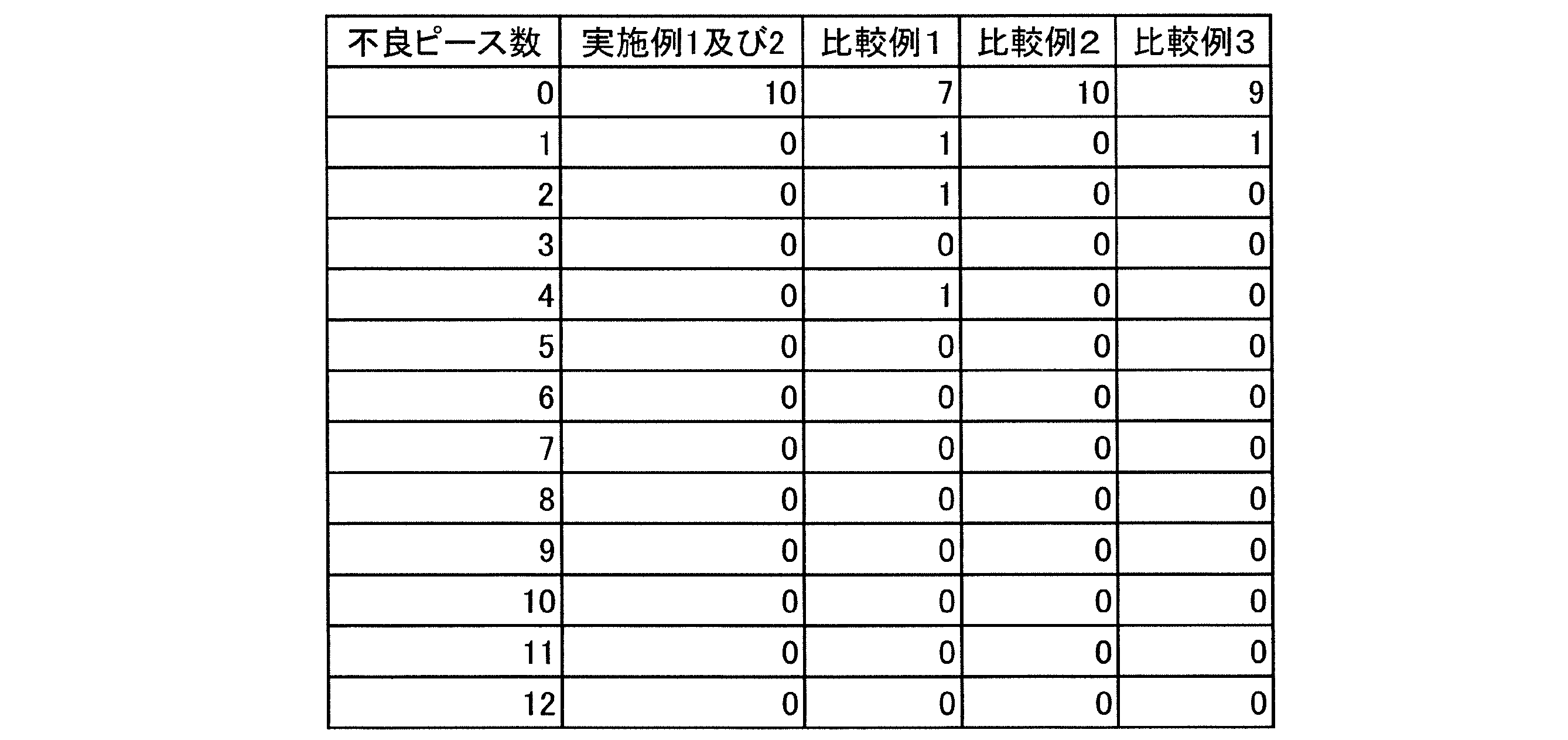
表中に示すとおり、一次実装において、めっき層を含む金属部が、周りの絶縁樹脂部9より低くなっている実施例1は、半田ボールの確実な配置ができている。
また、二次実装まで行ったサンプルの評価においては、比較例2、または、比較例3のように、めっき層を含む金属部が、周りの絶縁樹脂部9から突出しているほうが、接続信頼性が高くなっている。これは、図13中に示すように、半田バンプを形成する際に、突出した金属部の側面にも密着して、接着面積を上げるためである。
また、二次実装まで行ったサンプルの評価においては、比較例2、または、比較例3のように、めっき層を含む金属部が、周りの絶縁樹脂部9から突出しているほうが、接続信頼性が高くなっている。これは、図13中に示すように、半田バンプを形成する際に、突出した金属部の側面にも密着して、接着面積を上げるためである。
実施例1においても、不良数はゼロであるが、これは上記の理由とは別であり、電極の周りにある絶縁樹脂の壁の存在が、今回の材料構成、基板構造においては、接続信頼性を高めるほうに働いたためである。
別の材料構成、基板構造であれば、金属部の高さと接続信頼性の関係は、今回とは変わる可能性があり、めっき前の段階で、金属部の高さを、絶縁樹脂部9よりも低くしておき、状況によって、後のめっき工程にて高さを調節できるようにするのが好ましい。
以上で、特定の実施形態を参照して本発明を説明したが、これら説明によって発明を限定することを意図するものではない。本発明の説明を参照することにより、当業者には、開示された実施形態とともに本発明の別の実施形態も明らかである。従って、請求の範囲は、本発明の範囲及び要旨に含まれるこれらの変形例または実施形態も網羅すると解すべきである。
別の材料構成、基板構造であれば、金属部の高さと接続信頼性の関係は、今回とは変わる可能性があり、めっき前の段階で、金属部の高さを、絶縁樹脂部9よりも低くしておき、状況によって、後のめっき工程にて高さを調節できるようにするのが好ましい。
以上で、特定の実施形態を参照して本発明を説明したが、これら説明によって発明を限定することを意図するものではない。本発明の説明を参照することにより、当業者には、開示された実施形態とともに本発明の別の実施形態も明らかである。従って、請求の範囲は、本発明の範囲及び要旨に含まれるこれらの変形例または実施形態も網羅すると解すべきである。
上記実施形態及び上記実施例で説明したように、本発明の一態様に係る樹脂付リードフレーム基板及びその製造方法であれば、本発明が解決しようとする課題を解決し得る。以下、本発明の一態様に係る樹脂付リードフレーム基板及びその製造方法が解決した課題の詳細について、説明する。
ウェハープロセスで製造される各種のメモリー、CMOS、CPU、FPGA等の半導体素子は、電気的接続用端子を有する。
電気的接続用端子のピッチと、半導体素子が装着されるプリント基板側の接続部のピッチとは、工法の違いから、そのスケールが1~2桁ほど異なる。そのため、インターポーザーと称される、ピッチ変換のための仲介用基板(半導体素子実装用基板)が使用される。
ウェハープロセスで製造される各種のメモリー、CMOS、CPU、FPGA等の半導体素子は、電気的接続用端子を有する。
電気的接続用端子のピッチと、半導体素子が装着されるプリント基板側の接続部のピッチとは、工法の違いから、そのスケールが1~2桁ほど異なる。そのため、インターポーザーと称される、ピッチ変換のための仲介用基板(半導体素子実装用基板)が使用される。
インターポーザーの一方の面には、半導体素子を実装し、インターポーザーの他方の面、または、基板の周辺部で、プリント基板との接続がとられる。
また、インターポーザーは、内部または表面に金属製のリードフレームを有している。そして、このリードフレームにより電気的経路を引き回して、プリント基板との接続を行うことにより、外部接続端子のピッチを拡張している。
図17は、インターポーザーの一例として、QFN(Quad Flat Non-leaded)式リードフレームの構造を模式的に示す図である。
図17中に示すQFN式リードフレームは、まず、ポリイミドテープからなる保持材14に貼り付けられたリードフレームの所定箇所に、半導体素子11を、固定用樹脂16、または、固定用テープで固定する。その後、ワイヤーボンディングを行い、トランスファーモールド工法で複数のチップ(半導体素子11)を、一括で樹脂モールドする。最後に、外装加工を施し、個々に切断、断裁して完成品となる。
また、インターポーザーは、内部または表面に金属製のリードフレームを有している。そして、このリードフレームにより電気的経路を引き回して、プリント基板との接続を行うことにより、外部接続端子のピッチを拡張している。
図17は、インターポーザーの一例として、QFN(Quad Flat Non-leaded)式リードフレームの構造を模式的に示す図である。
図17中に示すQFN式リードフレームは、まず、ポリイミドテープからなる保持材14に貼り付けられたリードフレームの所定箇所に、半導体素子11を、固定用樹脂16、または、固定用テープで固定する。その後、ワイヤーボンディングを行い、トランスファーモールド工法で複数のチップ(半導体素子11)を、一括で樹脂モールドする。最後に、外装加工を施し、個々に切断、断裁して完成品となる。
すなわち、図17(a)に示すように、QFN式リードフレームは、銅、アルミニウム等の金属からなるリードフレームの中央部に、半導体素子11を搭載する平坦部12を設け、外周部にピッチの広いリード4(図示せず)を配設したものである。そして、リード4と半導体素子11の電気的接続用端子との接続には、金線等のメタルワイヤー13によるボンディング法を使用する。
なお、図17(a)及び図17(b)中に示す保持材14は、リードフレームを保持するものであり、図17(c)中に示すように、絶縁樹脂(モールド用樹脂17)によるモールド後に除去される。しかし、図17中に示すインターポーザーでは、電気的接続が半導体素子の外周部とリードフレームの外周部でしか行えないので、端子数が多い半導体基板には不向きといえる。
なお、図17(a)及び図17(b)中に示す保持材14は、リードフレームを保持するものであり、図17(c)中に示すように、絶縁樹脂(モールド用樹脂17)によるモールド後に除去される。しかし、図17中に示すインターポーザーでは、電気的接続が半導体素子の外周部とリードフレームの外周部でしか行えないので、端子数が多い半導体基板には不向きといえる。
プリント基板とインターポーザーの接続は、端子数が少ない場合には、インターポーザーの外延部の取り出し電極15に、金属ピンを装着して行われる。また、端子数が多い場合には、外周部分の外部接続端子に、半田ボールをアレイ状に配置(Ball Grid Array)する。プリント基板側の接続ピッチは500μm程度と広く、半田量も多いので、Ball Grid Arrayは、安定した高信頼性の接続が可能である。
面積が狭く端子数が多い半導体素子に対しては、電気的経路が一層のインターポーザーでは、ピッチの変換が困難なので、電気的経路を有する層を、2層、3層と、多層で積層化している。
一方、面積が狭く端子数が多い半導体素子の場合、半導体素子の接続端子は、半導体素子の底面にアレイ状に配置して形成されることが多い。そのため、インターポーザー側の外部接続端子も、同一なアレイ状の配置として、インターポーザーとプリント基板との接続には、微小な半田ボールを用いるフリップチップ接続方式が採用される。
面積が狭く端子数が多い半導体素子に対しては、電気的経路が一層のインターポーザーでは、ピッチの変換が困難なので、電気的経路を有する層を、2層、3層と、多層で積層化している。
一方、面積が狭く端子数が多い半導体素子の場合、半導体素子の接続端子は、半導体素子の底面にアレイ状に配置して形成されることが多い。そのため、インターポーザー側の外部接続端子も、同一なアレイ状の配置として、インターポーザーとプリント基板との接続には、微小な半田ボールを用いるフリップチップ接続方式が採用される。
インターポーザー内の配線は、上部から垂直方向にドリルまたはレーザーで窄孔し、孔内に金属めっきを行うことによって、上下の電気的導通がなされる。この方式のインターポーザーでは、外部接続端子のピッチは150μm以上200μm以下の範囲内程度まで微細化できるため、接続端子数は稼げるが、接合の信頼性や安定性は低下する。このため、この方式のインターポーザーは、高い信頼性が要求される車載用等には向いていない。
このようなインターポーザーは、使用する材料や構造により、リードフレーム部分が保持される基材がセラミックのもの、あるいは、P-BGA(Plastic Ball Grid Array)、CSP(Chip Size Package)、LGA(Land Grid Array)等のように、基材が有機物のもの等、数種類あり、目的に応じて使い分けられている。
このようなインターポーザーは、使用する材料や構造により、リードフレーム部分が保持される基材がセラミックのもの、あるいは、P-BGA(Plastic Ball Grid Array)、CSP(Chip Size Package)、LGA(Land Grid Array)等のように、基材が有機物のもの等、数種類あり、目的に応じて使い分けられている。
いずれの場合であっても、半導体素子の小型化、多ピン化、高速化に対応して、インターポーザーの半導体素子との接続部のファインピッチ化及び高速信号対応が進んでいる。微細化の進展を考慮すると、端子部分のピッチは、80μm以上100μm以下の範囲内が必要である。
導通部兼支持部材でもあるリードフレームは、薄い金属板をエッチングして製造する、いわゆるフォトエッチング法で形成される。ここで、安定したエッチング処理と、その後の加工での基材のハンドリングを容易にするには、上述の金属板は、200μm程度の厚さを有することが望ましい。
導通部兼支持部材でもあるリードフレームは、薄い金属板をエッチングして製造する、いわゆるフォトエッチング法で形成される。ここで、安定したエッチング処理と、その後の加工での基材のハンドリングを容易にするには、上述の金属板は、200μm程度の厚さを有することが望ましい。
また、ワイヤーボンディングの際に十分な接合強度を得るには、一定程度の金属層の厚みと、ランド面積が必要となる。これら双方の点を考慮すると、金属板の厚みとしては、200μm程度が必要最低といえる。その場合、金属板の両側から、エッチングを行うことが好適である。
また、リードフレームの裏面18(半導体素子11が搭載される面とは反対側の面)を被覆するポリイミドテープからなる保持材14は、リードフレームの裏面18がプリント基板との接続面となる場合、モールド時にモールド用樹脂17がリード裏面の接続端子面に回りこみ付着しないようにするため、不可欠である。
また、リードフレームの裏面18(半導体素子11が搭載される面とは反対側の面)を被覆するポリイミドテープからなる保持材14は、リードフレームの裏面18がプリント基板との接続面となる場合、モールド時にモールド用樹脂17がリード裏面の接続端子面に回りこみ付着しないようにするため、不可欠である。
しかしながら、最終的には、ポリイミドテープからなる保持材14は不要であるので、モールド加工をした後は、取り外して捨てることになる。そのため、リードフレームを保持材14に貼り付けてインターポーザーを製造する方法は、コストがかかるという問題を抱えていた。
上記の問題を解決する技術として、パターンエッチング、ハーフエッチング等を用いて、金属板の両面に凹凸、または、貫通孔を形成し、形成した部分に絶縁樹脂を成型して作るリードフレーム型基板が挙げられる(例えば、特許文献1を参照)。
この構造の基板であれば、絶縁樹脂が、配線パターンを支持する機能を有するため、ポリイミドテープを貼付する必要がなく、コストダウンを実現することが可能となる。
上記の問題を解決する技術として、パターンエッチング、ハーフエッチング等を用いて、金属板の両面に凹凸、または、貫通孔を形成し、形成した部分に絶縁樹脂を成型して作るリードフレーム型基板が挙げられる(例えば、特許文献1を参照)。
この構造の基板であれば、絶縁樹脂が、配線パターンを支持する機能を有するため、ポリイミドテープを貼付する必要がなく、コストダウンを実現することが可能となる。
ところで、上記のように形成した電子基板に素子を実装する場合、従来技術のように、金属部(配線パターン)と絶縁樹脂部との高さが揃っていると、接続信頼性等の観点から、望ましくない場合が多い。例えば、樹脂付リードフレーム基板の裏面の接続パッド上に、半田ボールを配置し、リフロー工程を経て半田バンプを形成する場合、接続パッドとその周りの絶縁樹脂部とが同一平面にあると、半田ボールの脱落が起こりやすく、接続信頼性を損なう可能性が高くなる。
また、基板やそれを部品とする半導体パッケージの構造や要求品質によっては、半田ボールと接続パッドの接続強度や横方向からの応力に対するシェア強度を得るために、接続パッドと周囲の絶縁樹脂部とが同一平面にあるのが適切でない場合もある。
また、この構造の樹脂付リードフレーム基板を得る場合に最も困難かつ重要なのは、金属除去部を確実に絶縁樹脂で代替することであり、そのための手段としてトランスファーモールド工法を使用した場合、その際に生じた樹脂バリをいかにして除去するかが問題となる。このため、簡便で安価で、かつ確実なバリ除去方法が必要である。
以上のように、従来技術に係る樹脂付リードフレーム基板には、樹脂付リードフレーム基板と半田ボールとの接続信頼性が低くなることがあるといった課題がある。
また、基板やそれを部品とする半導体パッケージの構造や要求品質によっては、半田ボールと接続パッドの接続強度や横方向からの応力に対するシェア強度を得るために、接続パッドと周囲の絶縁樹脂部とが同一平面にあるのが適切でない場合もある。
また、この構造の樹脂付リードフレーム基板を得る場合に最も困難かつ重要なのは、金属除去部を確実に絶縁樹脂で代替することであり、そのための手段としてトランスファーモールド工法を使用した場合、その際に生じた樹脂バリをいかにして除去するかが問題となる。このため、簡便で安価で、かつ確実なバリ除去方法が必要である。
以上のように、従来技術に係る樹脂付リードフレーム基板には、樹脂付リードフレーム基板と半田ボールとの接続信頼性が低くなることがあるといった課題がある。
(本実施形態の効果)
(1)上記課題を有する従来技術に係る樹脂付リードフレーム基板に対し、本実施形態に係る樹脂付リードフレーム基板FRBは、金属基材1の少なくとも一方の面の一部から金属基材1の板厚が減少するように金属を除去して形成した配線パターン部(例えば、リード4、電極パッド5、表面ダイパッド7、裏面ダイパッド8)を備えるリードフレーム25と、その金属を除去した部分の絶縁樹脂による代替で形成された絶縁樹脂部9と、を備えている。そして、絶縁樹脂部9の高さは、配線パターン部の高さよりも3μm以上高くなっている。
このような構成であれば、樹脂付リードフレーム基板FRBの表面において、配線パターン部の一部である接続パッド部(例えば、電極パッド5、表面ダイパッド7、裏面ダイパッド8)の高さを周りの絶縁樹脂部9よりも低くすることが可能となる。このため、本実施形態に係る樹脂付リードフレーム基板FRBであれば、半田との接続信頼性を向上させることが可能となる。
(1)上記課題を有する従来技術に係る樹脂付リードフレーム基板に対し、本実施形態に係る樹脂付リードフレーム基板FRBは、金属基材1の少なくとも一方の面の一部から金属基材1の板厚が減少するように金属を除去して形成した配線パターン部(例えば、リード4、電極パッド5、表面ダイパッド7、裏面ダイパッド8)を備えるリードフレーム25と、その金属を除去した部分の絶縁樹脂による代替で形成された絶縁樹脂部9と、を備えている。そして、絶縁樹脂部9の高さは、配線パターン部の高さよりも3μm以上高くなっている。
このような構成であれば、樹脂付リードフレーム基板FRBの表面において、配線パターン部の一部である接続パッド部(例えば、電極パッド5、表面ダイパッド7、裏面ダイパッド8)の高さを周りの絶縁樹脂部9よりも低くすることが可能となる。このため、本実施形態に係る樹脂付リードフレーム基板FRBであれば、半田との接続信頼性を向上させることが可能となる。
(2)また、本実施形態に係る配線パターン部上に形成されためっき層10を備えていてもよい。
このような構成であれば、接続パッド部の高さをめっきによって周りの絶縁樹脂部9よりも高くするという調節も可能となる。このような形態の樹脂付リードフレーム基板FRBであっても、半田との接続信頼性を向上させることが可能である。
このような構成であれば、接続パッド部の高さをめっきによって周りの絶縁樹脂部9よりも高くするという調節も可能となる。このような形態の樹脂付リードフレーム基板FRBであっても、半田との接続信頼性を向上させることが可能である。
(3)また、本実施形態に係る樹脂付リードフレーム基板の製造方法は、金属基材1の少なくとも一方の面の一部から金属基材1の板厚が減少するように金属を除去して所定の配線パターンを形成する配線パターン形成工程と、その金属を除去した部分を絶縁樹脂で代替し、金属基材1の配線パターンが形成された配線パターン部の高さよりも高い絶縁樹脂部9を形成する絶縁樹脂部形成工程と、を含んでいる。そして、絶縁樹脂部形成工程は、金属を除去した後の金属基材1を上金型21及び下金型22で厚さ方向から型締めした状態において形成されるキャビティ内に溶融させた絶縁樹脂23を充填する絶縁樹脂充填工程と、絶縁樹脂充填工程で充填した絶縁樹脂23を固化させる溶融絶縁樹脂固化工程と、を含んでいる。
このような構成であれば、樹脂付リードフレーム基板FRBの表面において、上述した接続パッド部の高さを周りの絶縁樹脂部9よりも低くすることが可能となる。このため、本実施形態に係る樹脂付リードフレーム基板FRBの製造方法であれば、半田との接続信頼性を向上させた樹脂付リードフレーム基板を提供することが可能となる。
このような構成であれば、樹脂付リードフレーム基板FRBの表面において、上述した接続パッド部の高さを周りの絶縁樹脂部9よりも低くすることが可能となる。このため、本実施形態に係る樹脂付リードフレーム基板FRBの製造方法であれば、半田との接続信頼性を向上させた樹脂付リードフレーム基板を提供することが可能となる。
(4)また、本実施形態に係る配線パターン形成工程では、金属を除去する部分以外にレジストパターン3を形成してエッチングすることで金属基材1の少なくとも一部を除去してもよい。また、絶縁樹脂部形成工程は、レジストパターン3を残した状態でキャビティ内に充填した絶縁樹脂23を固化させた後に、レジストパターン3を除去するパターン除去工程を含んでもよい。
このような構成であれば、絶縁樹脂部形成工程の際に発生した樹脂バリ24を、パターン除去工程において、レジストパターン3とともに確実に除去することが可能となる。このため、バリ残りによるめっき不良等を防止することが可能となる。
よって、本実施形態に係る樹脂付リードフレーム基板RFBの製造方法であれば、樹脂付リードフレーム基板RFBの製造過程における樹脂バリ24の、簡便かつ確実な除去方法を提供することが可能となる。
このような構成であれば、絶縁樹脂部形成工程の際に発生した樹脂バリ24を、パターン除去工程において、レジストパターン3とともに確実に除去することが可能となる。このため、バリ残りによるめっき不良等を防止することが可能となる。
よって、本実施形態に係る樹脂付リードフレーム基板RFBの製造方法であれば、樹脂付リードフレーム基板RFBの製造過程における樹脂バリ24の、簡便かつ確実な除去方法を提供することが可能となる。
(5)また、本実施形態に係るレジストパターン3の厚さ(膜厚)を、3μm以上としてもよい。
このような構成であれば、レジストパターン3は、エッチングにおけるマスクとしての役割(機能)を果たし得る。なお、レジストパターン3の厚さが3μm未満であると、エッチングの際に、レジストパターン3のマスクとしての役割を果たさないことがある。
また、このような構成であれば、樹脂付リードフレーム基板FRBの表面において、配線パターン部の一部である接続パッド部の高さを周りの絶縁樹脂部9よりも3μm以上低くすることが可能となる。このため、本実施形態に係る樹脂付リードフレーム基板FRBの製造方法であれば、半田との接続信頼性を向上させた樹脂付リードフレーム基板を提供することが可能となる。
このような構成であれば、レジストパターン3は、エッチングにおけるマスクとしての役割(機能)を果たし得る。なお、レジストパターン3の厚さが3μm未満であると、エッチングの際に、レジストパターン3のマスクとしての役割を果たさないことがある。
また、このような構成であれば、樹脂付リードフレーム基板FRBの表面において、配線パターン部の一部である接続パッド部の高さを周りの絶縁樹脂部9よりも3μm以上低くすることが可能となる。このため、本実施形態に係る樹脂付リードフレーム基板FRBの製造方法であれば、半田との接続信頼性を向上させた樹脂付リードフレーム基板を提供することが可能となる。
(6)また、本実施形態に係る樹脂付リードフレーム基板の製造方法は、絶縁樹脂部形成工程の後に、配線パターン部上にめっき層10を形成するめっき層形成工程を含んでもよい。
このような構成であれば、配線パターン部の一部である接続パッド部の高さをめっきによって周りの絶縁樹脂部9よりも高くするという調節も可能となる。このような形態の樹脂付リードフレーム基板FRBの製造方法であっても、半田との接続信頼性を向上させた樹脂付リードフレーム基板を提供することは可能である。
このような構成であれば、配線パターン部の一部である接続パッド部の高さをめっきによって周りの絶縁樹脂部9よりも高くするという調節も可能となる。このような形態の樹脂付リードフレーム基板FRBの製造方法であっても、半田との接続信頼性を向上させた樹脂付リードフレーム基板を提供することは可能である。
本発明は、半導体素子を実装するための半導体基板に関し、特に、リードフレーム型基板及びその製造方法に利用することが可能である。
1…金属基材、2…感光性レジスト、3…レジストパターン、4…リード、5…電極パッド、6…半田ボール、7…表面ダイパッド、8…裏面ダイパッド、9…絶縁樹脂部、10…めっき層、11…半導体素子、12…平坦部、13…メタルワイヤー、14…保持材、15…取り出し電極、16…固定用樹脂、17…モールド用樹脂、18…リードフレームの裏面、19…吊りリード、20…タイバー、21…上金型、22…下金型、23…溶融させた絶縁樹脂、24…樹脂バリ、25…リードフレーム、RFB…樹脂付リードフレーム基板
Claims (6)
- 金属基材の少なくとも一方の面の一部から前記金属基材の板厚が減少するように金属を除去して形成した配線パターン部を備えたリードフレームと、
前記金属を除去した部分の絶縁樹脂による代替で形成された絶縁樹脂部と、を備え、
前記絶縁樹脂部の高さは、前記配線パターン部の高さよりも3μm以上高いことを特徴とする樹脂付リードフレーム基板。 - 前記配線パターン部上に形成されためっき層を備えたことを特徴とする請求項1に記載した樹脂付リードフレーム基板。
- 金属基材の少なくとも一方の面の一部から前記金属基材の板厚が減少するように金属を除去して所定の配線パターンを形成する配線パターン形成工程と、
前記金属を除去した部分を絶縁樹脂で代替し、前記金属基材の前記配線パターンが形成された配線パターン部の高さよりも高い絶縁樹脂部を形成する絶縁樹脂部形成工程と、を含み、
前記絶縁樹脂部形成工程は、前記金属を除去した後の前記金属基材を上金型及び下金型で厚さ方向から型締めした状態において形成されるキャビティ内に溶融した前記絶縁樹脂を充填する絶縁樹脂充填工程と、前記絶縁樹脂充填工程で充填した前記絶縁樹脂を固化させる溶融絶縁樹脂固化工程と、を含むことを特徴とする樹脂付リードフレーム基板の製造方法。 - 前記配線パターン形成工程では、前記金属を除去する部分以外にレジストパターンを形成してエッチングすることで前記金属基材の少なくとも一部を除去し、
前記絶縁樹脂部形成工程は、前記レジストパターンを残した状態で前記キャビティ内に充填した前記絶縁樹脂を固化させた後に、前記レジストパターンを除去するパターン除去工程を含むことを特徴とする請求項3に記載した樹脂付リードフレーム基板の製造方法。 - 前記レジストパターンの厚さを、3μm以上とすることを特徴とする請求項4に記載した樹脂付リードフレーム基板の製造方法。
- 前記絶縁樹脂部形成工程の後に、前記配線パターン部上にめっき層を形成するめっき層形成工程を含むことを特徴とする請求項3から請求項5のいずれか1項に記載した樹脂付リードフレーム基板の製造方法。
Applications Claiming Priority (2)
| Application Number | Priority Date | Filing Date | Title |
|---|---|---|---|
| JP2014129109A JP2016009746A (ja) | 2014-06-24 | 2014-06-24 | 樹脂付リードフレーム基板及びその製造方法 |
| JP2014-129109 | 2014-06-24 |
Publications (1)
| Publication Number | Publication Date |
|---|---|
| WO2015198533A1 true WO2015198533A1 (ja) | 2015-12-30 |
Family
ID=54937645
Family Applications (1)
| Application Number | Title | Priority Date | Filing Date |
|---|---|---|---|
| PCT/JP2015/002757 Ceased WO2015198533A1 (ja) | 2014-06-24 | 2015-06-01 | 樹脂付リードフレーム基板及びその製造方法 |
Country Status (3)
| Country | Link |
|---|---|
| JP (1) | JP2016009746A (ja) |
| TW (1) | TW201606950A (ja) |
| WO (1) | WO2015198533A1 (ja) |
Cited By (1)
| Publication number | Priority date | Publication date | Assignee | Title |
|---|---|---|---|---|
| CN115985860A (zh) * | 2022-12-17 | 2023-04-18 | 西安微电子技术研究所 | 一种塑封器件外引线封装结构及返镀方法 |
Citations (2)
| Publication number | Priority date | Publication date | Assignee | Title |
|---|---|---|---|---|
| WO2010116622A1 (ja) * | 2009-03-30 | 2010-10-14 | 凸版印刷株式会社 | 半導体素子用基板の製造方法および半導体装置 |
| WO2010137899A2 (en) * | 2009-05-27 | 2010-12-02 | Lg Innotek Co., Ltd. | Leadframe and method for manufacturing the same |
-
2014
- 2014-06-24 JP JP2014129109A patent/JP2016009746A/ja active Pending
-
2015
- 2015-06-01 WO PCT/JP2015/002757 patent/WO2015198533A1/ja not_active Ceased
- 2015-06-23 TW TW104120082A patent/TW201606950A/zh unknown
Patent Citations (2)
| Publication number | Priority date | Publication date | Assignee | Title |
|---|---|---|---|---|
| WO2010116622A1 (ja) * | 2009-03-30 | 2010-10-14 | 凸版印刷株式会社 | 半導体素子用基板の製造方法および半導体装置 |
| WO2010137899A2 (en) * | 2009-05-27 | 2010-12-02 | Lg Innotek Co., Ltd. | Leadframe and method for manufacturing the same |
Cited By (2)
| Publication number | Priority date | Publication date | Assignee | Title |
|---|---|---|---|---|
| CN115985860A (zh) * | 2022-12-17 | 2023-04-18 | 西安微电子技术研究所 | 一种塑封器件外引线封装结构及返镀方法 |
| CN115985860B (zh) * | 2022-12-17 | 2026-04-10 | 西安微电子技术研究所 | 一种塑封器件外引线封装结构及返镀方法 |
Also Published As
| Publication number | Publication date |
|---|---|
| JP2016009746A (ja) | 2016-01-18 |
| TW201606950A (zh) | 2016-02-16 |
Similar Documents
| Publication | Publication Date | Title |
|---|---|---|
| CN102365737B (zh) | 半导体元件用基板的制造方法及半导体器件 | |
| KR101609016B1 (ko) | 반도체 소자용 기판의 제조 방법 및 반도체 장치 | |
| JP5629969B2 (ja) | リードフレーム型基板の製造方法と半導体装置の製造方法 | |
| US8390105B2 (en) | Lead frame substrate, manufacturing method thereof, and semiconductor apparatus | |
| CN102165585A (zh) | 引线框基板及其制造方法、半导体器件 | |
| JP5672652B2 (ja) | 半導体素子用基板の製造方法および半導体装置 | |
| KR20120010044A (ko) | 리드프레임 제조방법과 그에 따른 리드프레임 및 반도체 패키지 제조방법과 그에 따른 반도체 패키지 | |
| JP2009147117A (ja) | リードフレーム型基板の製造方法及び半導体基板 | |
| WO2015198533A1 (ja) | 樹脂付リードフレーム基板及びその製造方法 | |
| JP2015109295A (ja) | リードフレーム型基板およびリードフレーム型基板の製造方法 | |
| JP6589577B2 (ja) | 樹脂付リードフレーム基板の製造方法 | |
| JP2016122713A (ja) | リードフレーム基板およびその製造方法 | |
| JP2017130522A (ja) | 樹脂付リードフレーム基板 | |
| KR101025775B1 (ko) | 리드 프레임 및 이를 이용한 반도체 패키지의 제조 방법 | |
| JP4290259B2 (ja) | バンプグリッドアレイ半導体パッケージの製造方法 | |
| JP2004172647A (ja) | 半導体装置 | |
| KR20130084359A (ko) | 보드 레벨 신뢰성이 향상된 반도체 패키지용 인쇄회로기판 및 그 제조방법 |
Legal Events
| Date | Code | Title | Description |
|---|---|---|---|
| 121 | Ep: the epo has been informed by wipo that ep was designated in this application |
Ref document number: 15812384 Country of ref document: EP Kind code of ref document: A1 |
|
| NENP | Non-entry into the national phase |
Ref country code: DE |
|
| 122 | Ep: pct application non-entry in european phase |
Ref document number: 15812384 Country of ref document: EP Kind code of ref document: A1 |