WO2015190836A1 - 차동 전달 임피던스 증폭기 - Google Patents
차동 전달 임피던스 증폭기 Download PDFInfo
- Publication number
- WO2015190836A1 WO2015190836A1 PCT/KR2015/005859 KR2015005859W WO2015190836A1 WO 2015190836 A1 WO2015190836 A1 WO 2015190836A1 KR 2015005859 W KR2015005859 W KR 2015005859W WO 2015190836 A1 WO2015190836 A1 WO 2015190836A1
- Authority
- WO
- WIPO (PCT)
- Prior art keywords
- amplifier
- differential
- common
- source
- input node
- Prior art date
- Legal status (The legal status is an assumption and is not a legal conclusion. Google has not performed a legal analysis and makes no representation as to the accuracy of the status listed.)
- Ceased
Links
Images


Classifications
-
- H—ELECTRICITY
- H03—ELECTRONIC CIRCUITRY
- H03G—CONTROL OF AMPLIFICATION
- H03G1/00—Details of arrangements for controlling amplification
- H03G1/0005—Circuits characterised by the type of controlling devices operated by a controlling current or voltage signal
- H03G1/0035—Circuits characterised by the type of controlling devices operated by a controlling current or voltage signal using continuously variable impedance elements
-
- H—ELECTRICITY
- H03—ELECTRONIC CIRCUITRY
- H03F—AMPLIFIERS
- H03F3/00—Amplifiers with only discharge tubes or only semiconductor devices as amplifying elements
- H03F3/45—Differential amplifiers
-
- H—ELECTRICITY
- H03—ELECTRONIC CIRCUITRY
- H03F—AMPLIFIERS
- H03F1/00—Details of amplifiers with only discharge tubes, only semiconductor devices or only unspecified devices as amplifying elements
- H03F1/08—Modifications of amplifiers to reduce detrimental influences of internal impedances of amplifying elements
- H03F1/083—Modifications of amplifiers to reduce detrimental influences of internal impedances of amplifying elements in transistor amplifiers
- H03F1/086—Modifications of amplifiers to reduce detrimental influences of internal impedances of amplifying elements in transistor amplifiers with FET's
-
- H—ELECTRICITY
- H03—ELECTRONIC CIRCUITRY
- H03F—AMPLIFIERS
- H03F3/00—Amplifiers with only discharge tubes or only semiconductor devices as amplifying elements
- H03F3/26—Push-pull amplifiers; Phase-splitters therefor
- H03F3/265—Push-pull amplifiers; Phase-splitters therefor with field-effect transistors only
-
- H—ELECTRICITY
- H03—ELECTRONIC CIRCUITRY
- H03F—AMPLIFIERS
- H03F3/00—Amplifiers with only discharge tubes or only semiconductor devices as amplifying elements
- H03F3/45—Differential amplifiers
- H03F3/45071—Differential amplifiers with semiconductor devices only
-
- H—ELECTRICITY
- H03—ELECTRONIC CIRCUITRY
- H03F—AMPLIFIERS
- H03F3/00—Amplifiers with only discharge tubes or only semiconductor devices as amplifying elements
- H03F3/45—Differential amplifiers
- H03F3/45071—Differential amplifiers with semiconductor devices only
- H03F3/45076—Differential amplifiers with semiconductor devices only characterised by the way of implementation of the active amplifying circuit in the differential amplifier
-
- H—ELECTRICITY
- H03—ELECTRONIC CIRCUITRY
- H03F—AMPLIFIERS
- H03F3/00—Amplifiers with only discharge tubes or only semiconductor devices as amplifying elements
- H03F3/45—Differential amplifiers
- H03F3/45071—Differential amplifiers with semiconductor devices only
- H03F3/45076—Differential amplifiers with semiconductor devices only characterised by the way of implementation of the active amplifying circuit in the differential amplifier
- H03F3/45179—Differential amplifiers with semiconductor devices only characterised by the way of implementation of the active amplifying circuit in the differential amplifier using MOSFET transistors as the active amplifying circuit
-
- H—ELECTRICITY
- H03—ELECTRONIC CIRCUITRY
- H03F—AMPLIFIERS
- H03F3/00—Amplifiers with only discharge tubes or only semiconductor devices as amplifying elements
- H03F3/45—Differential amplifiers
- H03F3/45071—Differential amplifiers with semiconductor devices only
- H03F3/45479—Differential amplifiers with semiconductor devices only characterised by the way of common mode signal rejection
- H03F3/45632—Differential amplifiers with semiconductor devices only characterised by the way of common mode signal rejection in differential amplifiers with FET transistors as the active amplifying circuit
- H03F3/45636—Differential amplifiers with semiconductor devices only characterised by the way of common mode signal rejection in differential amplifiers with FET transistors as the active amplifying circuit by using feedback means
-
- H—ELECTRICITY
- H03—ELECTRONIC CIRCUITRY
- H03F—AMPLIFIERS
- H03F3/00—Amplifiers with only discharge tubes or only semiconductor devices as amplifying elements
- H03F3/45—Differential amplifiers
- H03F3/45071—Differential amplifiers with semiconductor devices only
- H03F3/45479—Differential amplifiers with semiconductor devices only characterised by the way of common mode signal rejection
- H03F3/45632—Differential amplifiers with semiconductor devices only characterised by the way of common mode signal rejection in differential amplifiers with FET transistors as the active amplifying circuit
- H03F3/45636—Differential amplifiers with semiconductor devices only characterised by the way of common mode signal rejection in differential amplifiers with FET transistors as the active amplifying circuit by using feedback means
- H03F3/45641—Measuring at the loading circuit of the differential amplifier
- H03F3/45659—Controlling the loading circuit of the differential amplifier
-
- H—ELECTRICITY
- H03—ELECTRONIC CIRCUITRY
- H03G—CONTROL OF AMPLIFICATION
- H03G1/00—Details of arrangements for controlling amplification
- H03G1/0005—Circuits characterised by the type of controlling devices operated by a controlling current or voltage signal
- H03G1/0017—Circuits characterised by the type of controlling devices operated by a controlling current or voltage signal the device being at least one of the amplifying solid-state elements
- H03G1/0029—Circuits characterised by the type of controlling devices operated by a controlling current or voltage signal the device being at least one of the amplifying solid-state elements using field-effect transistors [FET]
-
- H—ELECTRICITY
- H03—ELECTRONIC CIRCUITRY
- H03F—AMPLIFIERS
- H03F2200/00—Indexing scheme relating to amplifiers
- H03F2200/541—Transformer coupled at the output of an amplifier
-
- H—ELECTRICITY
- H03—ELECTRONIC CIRCUITRY
- H03F—AMPLIFIERS
- H03F2200/00—Indexing scheme relating to amplifiers
- H03F2200/72—Indexing scheme relating to amplifiers the amplifier stage being a common gate configuration MOSFET
-
- H—ELECTRICITY
- H03—ELECTRONIC CIRCUITRY
- H03F—AMPLIFIERS
- H03F2200/00—Indexing scheme relating to amplifiers
- H03F2200/75—Indexing scheme relating to amplifiers the amplifier stage being a common source configuration MOSFET
-
- H—ELECTRICITY
- H03—ELECTRONIC CIRCUITRY
- H03F—AMPLIFIERS
- H03F2203/00—Indexing scheme relating to amplifiers with only discharge tubes or only semiconductor devices as amplifying elements covered by H03F3/00
- H03F2203/45—Indexing scheme relating to differential amplifiers
- H03F2203/45288—Differential amplifier with circuit arrangements to enhance the transconductance
Definitions
- the present invention relates to a differential transfer impedance amplifier.
- the transfer impedance amplifier refers to an amplifier of a type that receives a current and outputs a voltage signal. Transfer impedance amplifiers are used in receivers for high-speed communications such as optical receivers for 100 Gb Ethernet, optical links or board to board interconnects. As a prior art document relating to such a transfer impedance amplifier, there is Korean Patent Application Publication No. 2010-0138057 filed by the present applicant.
- the conventional transfer impedance amplifier has a structure in which one output is obtained from one input signal in a single ended configuration. Therefore, when the transfer impedance amplifier is used in a receiver or the like where noise sensitivity is important, the influence of power supply noise and ground noise is severe.
- a single pass-to-differential conversion circuit is added, so a low pass filter must be implemented, thereby increasing die size.
- the use of a replica circuit eliminates the use of single-to-differential conversion circuits, but also has the disadvantage of increased die size and power consumption.
- the present invention has been made to solve the above-mentioned problems of the prior art, and to provide a differential transfer impedance amplifier capable of obtaining a differential output for an input signal without increasing die size and power consumption as compared with the prior art.
- a differential transfer impedance amplifier has a common gate amplifier and a feedback resistor that receive an electrical signal from an input node, and a common source amplifier that receives an electrical signal from the input node. And the output signal of the common gate amplifier and the output signal of the common source amplifier form a differential signal pair.
- the output signals of the common gate amplifier and the common source amplifier each form a differential signal
- differential pairs can be implemented without forming a single-to-differential conversion circuit or a replication circuit, thereby reducing die size and power consumption.
- the advantage is that it can be reduced.
- the feedback resistance can be adjusted to adjust the input resistance of the common gate amplifier and the gain of the common source amplifier, thereby providing a symmetrical differential output by adjusting the feedback resistance.
- FIG. 1 is a circuit diagram schematically showing a differential transfer impedance amplifier according to an embodiment of the present invention.
- FIG. 2 is a schematic circuit diagram of a differential transfer impedance amplifier according to another embodiment of the present invention.
- FIG. 3 is a diagram showing the simulation and measurement results of the input impedance and the transfer impedance gain of the differential transfer impedance amplifier according to an embodiment of the present invention.
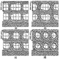
- FIG 4 is an eye diagram of the differential transimpedance amplifier according to the present embodiment.
- first and second are intended to distinguish one component from another component, and the scope of rights should not be limited by these terms.
- first component may be named a second component, and similarly, the second component may also be named a first component.
- each step may occur differently from the stated order unless the context clearly dictates the specific order. That is, each step may occur in the same order as specified, may be performed substantially simultaneously, or may be performed in the reverse order.
- a differential transfer impedance amplifier according to an embodiment of the present invention includes a common gate amplifier 100 and a common source amplifier 200 having a feedback resistor Rf.
- the common gate amplifier 100 is implemented with a metal oxide semiconductor transistor M1 and a load resistor R L , and an input current in1 is provided as a source of the common gate amplifier 100, and an output signal Vo1 is obtained from a drain. Is output.
- the gate of the common gate amplifier 100 is connected to an AC reference potential.
- the AC reference potential refers to a potential that does not change with time because there is no AC small signal component.
- the AC reference potential may be, for example, a ground potential.
- the AC reference potential may be a DC potential that provides a constant DC voltage without change with time.
- the input resistance Rin1 of the common gate amplifier 100 is the inverse of the transfer conductance gm1 of the transistor M1, and the voltage gain of the common gate amplifier 100 is gm 1 R L which is the product of the transfer conductance gm1 of M1 and the load resistance R L. Obtained. Accordingly, when the output voltage gain A1 for the input current is obtained by multiplying the voltage gain and the input resistance value, Equation 1 below.
- the transistor M1 serves as a current buffer, and the output current is applied to the load resistor R L to form the output voltage vo1.
- the current source Ibias provides the bias current. Since the operating point (Q point), the transfer conductance gm1, and the like of the transistor M1 included in the common gate amplifier are determined by the bias current by the current source, the input resistance Rin of the common gate amplifier is determined by the current applied by the current source.
- the common source amplifier 200 is provided between a gate and a transistor M2 having a gate provided with an input current in2 and a drain electrically connected to a source and a load electrically connected to a reference potential to provide an output signal vo2.
- the feedback resistor R F is connected.
- the output voltage gain A2 of the input current in2 of the common source amplifier having the feedback resistor is calculated as shown in Equation 2 below.
- gm2 is the transfer conductance of transistor M2, and R is the equivalent resistance of the load connected to transistor M2.
- Transistor M3, like transistor M1, has a gate connected to an AC reference power source and functions as an active load of M2. Therefore, R in Equation 2 is the equivalent resistance of M2 and load resistance R L seen from the drain of transistor M3.
- the output voltage gain with respect to the input current in2 of the common source amplifier 200 is negative, indicating that the phase of the input signal and the phase of the output signal are inverted with each other.
- the voltage gain with respect to the input current in the common gate amplifier 100 can be adjusted by adjusting the magnitude of the load resistance, and as can be seen in Equation 2, the common source amplifier 200 The gain of can be adjusted by adjusting the size of the feedback resistor (R F ).
- R F feedback resistor
- FIG. 2 is a schematic circuit diagram of a differential transfer impedance amplifier according to another embodiment of the present invention. Portions overlapping with the above-described embodiment may be omitted.
- the common gate amplifier 100 and the common source amplifier 200 provide output signals vo1 and vo2 through transformers XFM1 and XFM2. Transformers XFM1 and XFM2 reduce the effects of parasitic capacitance of the line. This improves bandwidth by allowing the transfer impedance amplifier to operate at higher speeds.
- the feedback resistor is divided into RF1 and RF2, respectively, and the voltage divided by the divided resistor is applied to the gate of the transistor M4 for control.
- the voltage applied to the gate of the transistor M4 to adjust the bias current of the transistor M1 included in the common gate amplifier, it is possible to adjust the input resistance of the common gate amplifier 100 accordingly.
- 3 is a simulation and measurement results of the trans impedance measurement result and the input stage input impedance of the differential transimpedance amplifier according to an embodiment of the present invention.
- a transimpedance amplifier receives a current formed by an optical receiving element such as a photodiode receiving an optical input and outputs it as a voltage signal. Accordingly, in order to receive a sufficient input of the current signal, unlike the voltage mode amplifier receiving the voltage signal, the input impedance is required to be low. It is also required to have an even gain over the entire frequency range over which the amplifier operates.
- the differential transimpedance amplifier according to the present embodiment has an even transimpedance gain (z21) of 50 to 55 db ⁇ up to 50 GHz as shown in FIG. 3, and has an input impedance (z11) of approximately 20 to 80 ⁇ in the same frequency band. Can be confirmed by simulation and measurement results.
- FIG. 4 is an eye diagram of the differential transimpedance amplifier according to the present embodiment.
- 4A shows 10Gb / s
- FIG. 4B shows 20Gb / s
- FIG. 4C shows 25Gb / s
- FIG. 4D shows eye diagram measurement results of a pseudo random binary sequence of 2 ⁇ 31 -1 of 32Gb / s. .
- the eyes are evenly opened in all frequency regions in which the differential transimpedance amplifier according to the embodiment of the present invention operates to provide high signal quality.
Landscapes
- Engineering & Computer Science (AREA)
- Power Engineering (AREA)
- Amplifiers (AREA)
Abstract
본 발명의 실시예에 의한 차동 전달 임피던스 증폭기는 입력 노드로부터 전기적 신호를 입력 받는 공통 게이트 증폭기(common gate amplifier) 및 피드백 저항을 가지고, 상기 입력 노드로부터 전기적 신호를 입력받는 공통 소스 증폭기(common source amplifier)를 포함하고, 공통 게이트 증폭기의 출력 신호와 상기 공통 소스 증폭기의 출력 신호는 차동 신호쌍(differential signal pair)을 이룬다.
Description
본 발명은 차동 전달 임피던스 증폭기에 관한 것이다.
전달 임피던스 증폭기는 전류를 입력받아 전압 신호를 출력하는 형태의 증폭기를 의미한다. 전달 임피던스 증폭기는 100Gb 이더넷용 광학 수신기, 광학 링크 또는 보드간 접속(board to board interconnect)등과 같이 고속 통신용 수신단에 활용된다. 이러한 전달 임피던스 증폭기에 관한 선행 문헌으로 본 출원인이 출원한 한국 공개특허 제2010-0138057가 있다.
종래의 전달 임피던스 증폭기는 단일단(single ended)구성으로 하나의 입력신호로부터 하나의 출력을 얻는 구조이다. 따라서 노이즈 민감도가 중요한 수신단 등에 전달 임피던스 증폭기를 활용하는 경우에 전원 노이즈 및 접지 노이즈에 의한 영향이 심하다.
노이즈에 의한 영향을 줄이기 위하여 단일단-차동단 변환 회로를 부가하는 경우에는 저역 통과 필터를 구현하여야 하므로 다이 사이즈가 커진다. 복제회로(replica circuit)를 이용하면 단일단-차동단 변환 회로를 사용하지 않으나, 마찬가지로 다이 사이즈 측면과 전력 소모가 증가한다는 단점이 있다.
본 발명은 상술한 종래 기술의 문제점을 해결하기 위한 것으로, 종래 기술에 비하여 다이 사이즈와 전력 소모를 증가시키지 않은 채로 입력 신호에 대하여 차동 출력을 얻을 수 있는 차동 전달 임피던스 증폭기를 제공하는 것이 본 발명의 목적 중 하나이다.
본 발명의 또다른 목적 중 하나는 피드백 저항값을 조절하여 회로의 입력 저항을 조절할 수 있는 차동 전달 임피던스 증폭기를 제공하는 것이다.
본 발명의 실시예에 의한 차동 전달 임피던스 증폭기는 입력 노드로부터 전기적 신호를 입력 받는 공통 게이트 증폭기(common gate amplifier) 및 피드백 저항을 가지고, 상기 입력 노드로부터 전기적 신호를 입력받는 공통 소스 증폭기(common source amplifier)를 포함하고, 공통 게이트 증폭기의 출력 신호와 상기 공통 소스 증폭기의 출력 신호는 차동 신호쌍(differential signal pair)을 이룬다.
본 발명의 실시예에 의하면 공통 게이트 증폭기와 공통 소스 증폭기의 출력 신호가 각각 차동 신호를 형성하므로, 단일단-차동단 변환 회로 또는 복제 회로를 형성하지 않고도 차동쌍을 구현할 수 있어서 다이 사이즈와 전력 소모을 줄일 수 있다는 장점이 제공된다.
또한, 피드백 저항을 조절하여 공통 게이트 증폭기의 입력 저항과 공통 소스 증폭기의 이득을 조절할 수 있어 피드백 저항을 조절하여 대칭적인 차동 출력을 얻을 수 있다는 장점도 또한 제공된다.
도 1은 본 발명의 실시예에 의한차동 전달 임피던스 증폭기를 개요적으로 도시한 회로도이다.
도 2는 본 발명의 다른 실시예에 따른 차동 전달 임피던스 증폭기에 대한 개요적 회로도이다.
도 3은 본 발명의 실시예에 의한 차동 전달 임피던스 증폭기의 입력 임피던스 및 전달 임피던스 이득의 모의시험 및 측정 결과를 도시한 도면이다.
도 4는 본 실시예에 의한 차동 트랜스 임피던스 증폭기의 아이 다이어그램(eye-diagram)이다.
본 발명에 관한 설명은 구조적 내지 기능적 설명을 위한 실시예에 불과하므로, 본 발명의 권리범위는 본문에 설명된 실시예에 의하여 제한되는 것으로 해석되어서는 아니 된다. 즉, 실시예는 다양한 변경이 가능하고 여러 가지 형태를 가질 수 있으므로 본 발명의 권리범위는 기술적 사상을 실현할 수 있는 균등물들을 포함하는 것으로 이해되어야 한다.
한편, 본 출원에서 서술되는 용어의 의미는 다음과 같이 이해되어야 할 것이다.
"제1", "제2" 등의 용어는 하나의 구성요소를 다른 구성요소로부터 구별하기 위한 것으로 이들 용어들에 의해 권리범위가 한정되어서는 아니 된다. 예를 들어, 제1 구성요소는 제2 구성요소로 명명될 수 있고, 유사하게 제2 구성요소도 제1 구성요소로 명명될 수 있다.
어떤 구성요소가 다른 구성요소에 "상부에" 또는 "위에"있다고 언급된 때에는, 그 다른 구성요소의 바로 위에 있을 수도 있지만, 중간에 다른 구성요소가 존재할 수도 있다고 이해되어야 할 것이다. 반면에, 어떤 구성요소가 다른 구성요소에 "접촉하여" 있다고 언급된 때에는, 중간에 다른 구성요소가 존재하지 않는 것으로 이해되어야 할 것이다. 한편, 구성요소들 간의 관계를 설명하는 다른 표현들, 즉 "개재하여"와 "바로 ~개재하여", "~사이에"와 "바로 ~ 사이에" 또는 "~에 이웃하는"과 "~에 직접 이웃하는" 등도 마찬가지로 해석되어야 한다.
단수의 표현은 문맥상 명백하게 다르게 뜻하지 않는 한 복수의 표현을 포함하는 것으로 이해되어야 하고, "포함하다" 또는 "가지다" 등의 용어는 설시된 특징, 숫자, 단계, 동작, 구성요소, 부분품 또는 이들을 조합한 것이 존재함을 지정하려는 것이지, 하나 또는 그 이상의 다른 특징들이나 숫자, 단계, 동작, 구성요소, 부분품 또는 이들을 조합한 것들의 존재 또는 부가 가능성을 미리 배제하지 않는 것으로 이해되어야 한다.
각 단계들은 문맥상 명백하게 특정 순서를 기재하지 않은 이상 명기된 순서와 다르게 일어날 수 있다. 즉, 각 단계들은 명기된 순서와 동일하게 일어날 수도 있고 실질적으로 동시에 수행될 수도 있으며 반대의 순서대로 수행될 수도 있다.
본 개시의 실시예들을 설명하기 위하여 참조되는 도면은 설명의 편의 및 이해의 용이를 위하여 의도적으로 크기, 높이, 두께 등이 과장되어 표현되어 있으며, 비율에 따라 확대 또는 축소된 것이 아니다. 또한, 도면에 도시된 어느 구성요소는 의도적으로 축소되어 표현하고, 다른 구성요소는 의도적으로 확대되어 표현될 수 있다.
여기서 사용되는 모든 용어들은 다르게 정의되지 않는 한, 본 발명이 속하는 분야에서 통상의 지식을 가진 자에 의해 일반적으로 이해되는 것과 동일한 의미를 가진다. 일반적으로 사용되는 사전에 정의되어 있는 것과 같은 용어들은 관련 기술의 문맥상 가지는 의미와 일치하는 것으로 해석되어야 하며, 본 출원에서 명백하게 정의하지 않는 한 이상적이거나 과도하게 형식적인 의미를 지니는 것으로 해석될 수 없다.
이하에서는 첨부된 도면을 참조하여 본 발명의 실시예에 따른 차동 전달 임피던스 증폭기를 설명한다. 도 1은 차동 전달 임피던스 증폭기를 개요적으로 도시한 회로도이다. 도 1을 참조하면, 본 발명에 따른 차동 전달 임피던스 증폭기는 공통 게이트 증폭기(common gate amplifier, 100)와 피드백 저항(Rf)을 가지는 공통 소스 증폭기(common source amplifier, 200)을 포함한다.
공통 게이트 증폭기(100)은 금속산화물반도체 트랜지스터 M1과 부하저항 RL로 구현되며, 공통 게이트 증폭기(100)의 소스(source)로 입력 전류(in1)가 제공되며, 출력 신호(Vo1)는 드레인으로부터 출력된다. 또한, 공통 게이트 증폭기(100)의 게이트(gate)는 교류 기준 전위에 연결된다. 교류 기준 전위는 교류 소신호 성분이 없어 교류적으로 보면 시간에 따른 변화가 없는 전위를 말한다. 교류 기준 전위는 일 예로, 접지 전위일 수 있으며, 다른 예로, 시간에 따라 변화 없는 일정한 직류 전압을 제공하는 직류 전위일 수 있다.
공통 게이트 증폭기(100)의 입력 저항(Rin1)은 트랜지스터 M1의 전달 컨덕턴스 gm1의 역수이며, 공통 게이트 증폭기(100)의 전압 이득은 M1의 전달 컨덕턴스 gm1과 부하저항 RL의 곱인 gm1RL로 얻어진다. 따라서, 전압 이득과 입력 저항값을 곱하여 입력 전류에 대한 출력 전압 이득(A1)을 구하면 아래의 수학식 1과 같다.

즉, 공통 게이트 증폭기에 있어서 트랜지스터 M1은 전류 버퍼(current buffer) 역할을 수행하며, 출력된 전류가 부하 저항(RL)에 인가되어 출력 전압 vo1을 형성하는 것을 알 수 있다.
전류원(Ibias)은 바이어스 전류를 제공한다. 공통 게이트 증폭기에 포함된 트랜지스터 M1의 동작점(Q point), 전달 컨덕턴스 gm1 등이 전류원에 의한 바이어스 전류에 의하여 결정되므로, 전류원이 인가하는 전류에 의하여 공통 게이트 증폭기의 입력 저항 Rin이 결정된다.
공통 소스 증폭기(200)는 입력 전류(in2)가 제공되는 게이트와 기준 전위에 전기적으로 연결된 소스 및 부하에 전기적으로 연결되어 출력 신호(vo2)를 제공하는 드레인을 가지는 트랜지스터 M2와 드레인과 게이트 사이에 연결되는 피드백 저항(RF)을 포함한다.
피드백 저항을 가지는 공통 소스 증폭기의 입력 전류(in2)에 대한 출력 전압 이득(A2)을 연산하면 아래의 수학식 2와 같다.

gm2는 트랜지스터 M2의 전달 컨덕턴스이며, R은 트랜지스터 M2에 연결된 부하의 등가저항을 의미한다. 트랜지스터 M3는 트랜지스터 M1과 마찬가지로 게이트가 교류 기준 전원에 연결되어 M2의 능동 부하(active load)로 기능한다. 따라서, 수학식 2의 R은 트랜지스터 M3의 드레인에서 바라보는 M2와 부하 저항 RL의 등가저항이다.
수학식 1과 달리 공통 소스 증폭기(200)의 입력 전류(in2)에 대한 출력 전압 이득은 -부호가 있어 입력 신호의 위상과 출력 신호의 위상은 서로 반전된 상태임을 알 수 있다. 수학식 1에서 알 수 있는 바와 같이 공통 게이트 증폭기(100)에 있어서 입력 전류에 대한 전압 이득은 부하 저항의 크기를 조절하여 조절할 수 있으며, 수학식 2에서 알 수 있는 바와 같이 공통 소스 증폭기(200)의 이득은 피드백 저항(RF)의 크기를 조절하여 조절할 수 있다. 따라서, 두 저항의 크기를 조절하면 하나의 입력 전류 신호(in)에 대하여 서로 상보적인 전압 신호 출력을 제공하는 차동 전달 임피던스 증폭기를 형성할 수 있다.
도 2는 본 발명의 다른 실시예에 따른 차동 전달 임피던스 증폭기에 대한 개요적 회로도이다. 위에서 설명된 실시예와 중복된 부분은 설명을 생략할 수 있다. 도 2를 참조하면, 공통 게이트 증폭기(100)과 공통 소스 증폭기(200)는 변압기(transformer, XFM1, XFM2)를 통하여 출력 신호(vo1, vo2)를 제공한다. 변압기(XFM1, XFM2)는 선로의 기생 커패시턴스(parasitic capacitance)에 의한 영향을 감소시킨다. 따라서 전달 임피던스 증폭기가 고속으로 동작할 수 있도록 하여 대역폭을 향상시킨다.
또한, 본 실시예에 있어서는 피드백 저항을 각각 RF1과 RF2로 분할하고, 분할된 저항에 의하여 분압된 전압을 트랜지스터 M4의 게이트에 인가하여 제어한다. 트랜지스터 M4의 게이트에 인가되는 전압을 제어하여 공통 게이트 증폭기에 포함된 트랜지스터 M1의 바이어스 전류를 조절할 수 있으며, 그에 따라 공통 게이트 증폭기(100)의 입력 저항을 조절할 수 있다.
모의 시험예
이하에서는 본 발명의 실시예에 따른 차동 트랜스 임피던스 증폭기의 모의 시험예를 첨부된 도면을 참조하여 설명한다. 도 3은 본 발명의 실시예에 따른 차동 트랜스 임피던스 증폭기의 트랜스 임피던스 측정결과와 입력단 입력 임피던스의 모의 시험 및 측정 결과이다.
트랜스 임피던스 증폭기는 일반적으로 광 다이오드(photo diode)와 같은 광 수신소자가 광 입력을 받아 형성한 전류를 수신하여 전압 신호로 출력한다. 따라서, 전류 신호를 충분하게 입력 받기 위하여는 전압 신호를 입력받는 전압 모드 증폭기와는 다르게 입력 임피던스가 낮을 것을 요구한다. 또한, 증폭기가 동작하는 전 주파수 영역 대에 있어서 고른 이득을 가질 것이 요청된다.
본 실시예에 의한 차동 트랜스 임피던스 증폭기는 도 3에 도시된 바와 같이 50GHz까지 50 내지 55 dbΩ의 고른 트랜스 임피던스 이득(z21)을 가지며, 동일한 주파수 대역에서 대략 20 내지 80Ω의 입력 임피던스(z11)를 가지는 것을 모의시험 및 측정 결과로 확인할 수 있다.
도 4는 본 실시예에 의한 차동 트랜스 임피던스 증폭기의 아이 다이어그램(eye-diagram)이다. 도 4a는 10Gb/s, 도 4b는 20Gb/s, 도 4c는 25Gb/s 그리고 도 4d는 32Gb/s의 2^31 -1의 의사 난수 이진 시퀀스(Pseudo Random Binary Sequence)의 아이 다이어그램 측정 결과이다. 각각의 도면에서 확인할 수 있는 바와 같이 본 발명의 실시예에 의한 차동 트랜스 임피던스 증폭기가 동작하는 전 주파수 영역에서 고르게 눈(eye)이 열려있어 높은 신호 품질을 제공하는 것을 확인할 수 있다.
본 발명에 대한 이해를 돕기 위하여 도면에 도시된 실시 예를 참고로 설명되었으나, 이는 실시를 위한 실시예로, 예시적인 것에 불과하며, 당해 분야에서 통상적 지식을 가진 자라면 이로부터 다양한 변형 및 균등한 타 실시 예가 가능하다는 점을 이해할 것이다. 따라서, 본 발명의 진정한 기술적 보호범위는 첨부된 특허청구범위에 의해 정해져야 할 것이다.
산업상 이용가능성은 상기에 기재되어 있음
Claims (7)
- 입력 노드로부터 전기적 신호를 입력 받는 공통 게이트 증폭기(common gate amplifier); 및피드백 저항을 가지고, 상기 입력 노드로부터 전기적 신호를 입력받는 공통 소스 증폭기(common source amplifier)를 포함하고,공통 게이트 증폭기의 출력 신호와 상기 공통 소스 증폭기의 출력 신호는 차동 신호쌍(differential signal pair)을 이루는 차동 전달 임피던스 증폭기(differential trans-impedance amplifier).
- 제1항에 있어서,상기 입력 노드에는 공통 게이트 증폭기의 입력 저항을 조절하는 차동 전류원이 전기적으로 연결된 전달 임피던스 증폭기.
- 제1항에 있어서,금속산화물반도체(Metal Oxide Silicon, MOS) 트랜지스터를 더 포함하되, 상기 MOS 트랜지스터는 입력 노드에 전기적으로 연결된 드레인과, 기준 전위에 전기적으로 연결된 소스 및 상기 피드백 저항에 의하여 조절되는 전압이 인가되는 게이트를 포함하는 차동 전달 임피던스 증폭기.
- 제1항에 있어서,상기 공통 게이트 증폭기는, 상기 입력 노드에 전기적으로 연결된 드레인과, 부하에 전기적으로 연결되어 출력 신호를 출력하는 소스 및 교류 기준 전위에 전기적으로 연결된 게이트를 가지는 MOS 트랜지스터를 포함하는 차동 전달 임피던스 증폭기.
- 제1항에 있어서,상기 공통 소스 증폭기는 기준 전위에 연결된 소스와, 상기 입력 노드에 전기적으로 연결된 게이트 및 부하에 전기적으로 연결되어 출력 신호를 출력하는 MOS 트랜지스터를 포함하는 차동 전달 임피던스 증폭기.
- 제1항에 있어서,상기 공통 게이트 증폭기와 상기 공통 소스 증폭기는 각각 기생 커패시턴스(parasitic capacitance)의 효과를 제거하는 트랜스포머(transformer)를 가지는 부하(load)를 포함하는 차동 전달 임피던스 증폭기.
- 제1항에 있어서,피드백 저항값을 조절하여 상기 공통 게이트 증폭기와 상기 공통 소스 증폭기의 이득(gain)을 매칭(matching)시키는 차동 전달 임피던스 증폭기(trans impedance amplifier).
Priority Applications (2)
| Application Number | Priority Date | Filing Date | Title |
|---|---|---|---|
| US15/311,122 US10348261B2 (en) | 2014-06-11 | 2015-06-11 | Differential transimpedance amplifier |
| US16/425,274 US10396734B1 (en) | 2014-06-11 | 2019-05-29 | Differential transimpedance amplifier |
Applications Claiming Priority (2)
| Application Number | Priority Date | Filing Date | Title |
|---|---|---|---|
| KR1020140070638A KR101715446B1 (ko) | 2014-06-11 | 2014-06-11 | 차동 전달 임피던스 증폭기 |
| KR10-2014-0070638 | 2014-06-11 |
Related Child Applications (2)
| Application Number | Title | Priority Date | Filing Date |
|---|---|---|---|
| US15/311,122 A-371-Of-International US10348261B2 (en) | 2014-06-11 | 2015-06-11 | Differential transimpedance amplifier |
| US16/425,274 Division US10396734B1 (en) | 2014-06-11 | 2019-05-29 | Differential transimpedance amplifier |
Publications (1)
| Publication Number | Publication Date |
|---|---|
| WO2015190836A1 true WO2015190836A1 (ko) | 2015-12-17 |
Family
ID=54833845
Family Applications (1)
| Application Number | Title | Priority Date | Filing Date |
|---|---|---|---|
| PCT/KR2015/005859 Ceased WO2015190836A1 (ko) | 2014-06-11 | 2015-06-11 | 차동 전달 임피던스 증폭기 |
Country Status (3)
| Country | Link |
|---|---|
| US (2) | US10348261B2 (ko) |
| KR (1) | KR101715446B1 (ko) |
| WO (1) | WO2015190836A1 (ko) |
Families Citing this family (1)
| Publication number | Priority date | Publication date | Assignee | Title |
|---|---|---|---|---|
| US10771280B1 (en) * | 2019-02-20 | 2020-09-08 | Texas Instruments Incorporated | Low-power wake-up circuit for controller area network (CAN) transceiver |
Citations (5)
| Publication number | Priority date | Publication date | Assignee | Title |
|---|---|---|---|---|
| US20020167357A1 (en) * | 2001-05-14 | 2002-11-14 | Stmicroelectronics S.A. | Differential amplifier comprising an unlocking device |
| US6566949B1 (en) * | 2000-08-31 | 2003-05-20 | International Business Machines Corporation | Highly linear high-speed transconductance amplifier for Gm-C filters |
| KR20080061480A (ko) * | 2006-12-28 | 2008-07-03 | 한국과학기술원 | Cmos 가변 이득 증폭기 |
| US20080290957A1 (en) * | 2006-01-30 | 2008-11-27 | University Of Washington | Receiver with colpitts differential oscillator, colpitts quadrature oscillator, and common-gate low noise amplifier |
| KR20100115843A (ko) * | 2009-04-21 | 2010-10-29 | 부산대학교 산학협력단 | 잡음과 왜곡 특성을 개선시키는 상보적 회로 |
Family Cites Families (6)
| Publication number | Priority date | Publication date | Assignee | Title |
|---|---|---|---|---|
| US6605993B2 (en) * | 2000-05-16 | 2003-08-12 | Fujitsu Limited | Operational amplifier circuit |
| JP3953009B2 (ja) * | 2003-09-12 | 2007-08-01 | ソニー株式会社 | トランスコンダクタンス調整回路 |
| US7760028B2 (en) * | 2004-11-26 | 2010-07-20 | St-Ericsson Sa | Transformer circuit |
| KR20100011584A (ko) | 2008-07-25 | 2010-02-03 | 삼성전기주식회사 | 경연성 인쇄회로기판 |
| KR101054388B1 (ko) | 2009-06-24 | 2011-08-04 | 이화여자대학교 산학협력단 | 광수신기용 트랜스임피던스 증폭기 |
| US9094634B2 (en) * | 2013-06-05 | 2015-07-28 | Silicon Laboratories Inc. | Amplifier for television tuner chip and method therefor |
-
2014
- 2014-06-11 KR KR1020140070638A patent/KR101715446B1/ko active Active
-
2015
- 2015-06-11 WO PCT/KR2015/005859 patent/WO2015190836A1/ko not_active Ceased
- 2015-06-11 US US15/311,122 patent/US10348261B2/en active Active
-
2019
- 2019-05-29 US US16/425,274 patent/US10396734B1/en active Active
Patent Citations (5)
| Publication number | Priority date | Publication date | Assignee | Title |
|---|---|---|---|---|
| US6566949B1 (en) * | 2000-08-31 | 2003-05-20 | International Business Machines Corporation | Highly linear high-speed transconductance amplifier for Gm-C filters |
| US20020167357A1 (en) * | 2001-05-14 | 2002-11-14 | Stmicroelectronics S.A. | Differential amplifier comprising an unlocking device |
| US20080290957A1 (en) * | 2006-01-30 | 2008-11-27 | University Of Washington | Receiver with colpitts differential oscillator, colpitts quadrature oscillator, and common-gate low noise amplifier |
| KR20080061480A (ko) * | 2006-12-28 | 2008-07-03 | 한국과학기술원 | Cmos 가변 이득 증폭기 |
| KR20100115843A (ko) * | 2009-04-21 | 2010-10-29 | 부산대학교 산학협력단 | 잡음과 왜곡 특성을 개선시키는 상보적 회로 |
Also Published As
| Publication number | Publication date |
|---|---|
| US20170077884A1 (en) | 2017-03-16 |
| US20190280662A1 (en) | 2019-09-12 |
| US10396734B1 (en) | 2019-08-27 |
| US10348261B2 (en) | 2019-07-09 |
| KR101715446B1 (ko) | 2017-03-14 |
| KR20150142234A (ko) | 2015-12-22 |
Similar Documents
| Publication | Publication Date | Title |
|---|---|---|
| WO2017071002A1 (en) | Combined low and high frequency continuous-time linear equalizers | |
| US20040239374A1 (en) | Differential signal receiving device and differential signal transmission system | |
| US10637695B1 (en) | High-speed low-voltage serial link receiver and method thereof | |
| EP3021482B1 (en) | Operational amplifier based circuit with compensation circuit block used for stability compensation | |
| WO2017082575A1 (ko) | 차동 전달 임피던스 증폭기 | |
| CN107005216A (zh) | 衰减器 | |
| US10797802B2 (en) | Optical receiver | |
| Chou et al. | A 40 Gbps optical receiver analog front-end in 65 nm CMOS | |
| WO2012068985A1 (zh) | 伪差分音频输入电路及其设置方法 | |
| GB2415339A (en) | A negative impedance receiver equaliser | |
| US6628168B2 (en) | Multiple input, fully differential, wide common-mode, folded-cascode amplifier | |
| US8582985B2 (en) | Input isolation of a transimpedance amplifier in optical receivers | |
| CN103379063A (zh) | 线性均衡器 | |
| JP2005167157A (ja) | 光・電気変換回路および電界検出光学装置 | |
| CN104348429B (zh) | 直流漂移消除电路 | |
| Ahmed | Transimpedance amplifier (TIA) design for 400 Gb/s optical fiber communications | |
| US20060097777A1 (en) | Architecture for transverse-form analog finite-impulse-response filter | |
| KR101715446B1 (ko) | 차동 전달 임피던스 증폭기 | |
| Ahmed et al. | A 100 Gb/s transimpedance amplifier in 65 nm CMOS technology for optical communications | |
| EP3404831B1 (en) | Photoreceiver with pre-equalizing differential transimpedance amplifier | |
| US11394376B2 (en) | Crosstalk cancellation circuit, transmitter, and transmission and reception system | |
| KR20090047619A (ko) | 광대역 증폭기 | |
| CN109891758B (zh) | 用于全双工传输的虚拟混合的电路和方法 | |
| JP2003258606A (ja) | 分散等化フィルタ回路 | |
| EP3272008A1 (en) | Negative feedback gain transimpedance amplifier (tia) systems |
Legal Events
| Date | Code | Title | Description |
|---|---|---|---|
| 121 | Ep: the epo has been informed by wipo that ep was designated in this application |
Ref document number: 15806830 Country of ref document: EP Kind code of ref document: A1 |
|
| WWE | Wipo information: entry into national phase |
Ref document number: 15311122 Country of ref document: US |
|
| NENP | Non-entry into the national phase |
Ref country code: DE |
|
| 122 | Ep: pct application non-entry in european phase |
Ref document number: 15806830 Country of ref document: EP Kind code of ref document: A1 |