WO2015190308A1 - 測距装置 - Google Patents
測距装置 Download PDFInfo
- Publication number
- WO2015190308A1 WO2015190308A1 PCT/JP2015/065458 JP2015065458W WO2015190308A1 WO 2015190308 A1 WO2015190308 A1 WO 2015190308A1 JP 2015065458 W JP2015065458 W JP 2015065458W WO 2015190308 A1 WO2015190308 A1 WO 2015190308A1
- Authority
- WO
- WIPO (PCT)
- Prior art keywords
- charge
- signal
- region
- transfer
- signal charge
- Prior art date
- Legal status (The legal status is an assumption and is not a legal conclusion. Google has not performed a legal analysis and makes no representation as to the accuracy of the status listed.)
- Ceased
Links
Images




Classifications
-
- G—PHYSICS
- G01—MEASURING; TESTING
- G01S—RADIO DIRECTION-FINDING; RADIO NAVIGATION; DETERMINING DISTANCE OR VELOCITY BY USE OF RADIO WAVES; LOCATING OR PRESENCE-DETECTING BY USE OF THE REFLECTION OR RERADIATION OF RADIO WAVES; ANALOGOUS ARRANGEMENTS USING OTHER WAVES
- G01S17/00—Systems using the reflection or reradiation of electromagnetic waves other than radio waves, e.g. lidar systems
- G01S17/02—Systems using the reflection of electromagnetic waves other than radio waves
- G01S17/06—Systems determining position data of a target
- G01S17/08—Systems determining position data of a target for measuring distance only
- G01S17/10—Systems determining position data of a target for measuring distance only using transmission of interrupted, pulse-modulated waves
-
- G—PHYSICS
- G01—MEASURING; TESTING
- G01S—RADIO DIRECTION-FINDING; RADIO NAVIGATION; DETERMINING DISTANCE OR VELOCITY BY USE OF RADIO WAVES; LOCATING OR PRESENCE-DETECTING BY USE OF THE REFLECTION OR RERADIATION OF RADIO WAVES; ANALOGOUS ARRANGEMENTS USING OTHER WAVES
- G01S17/00—Systems using the reflection or reradiation of electromagnetic waves other than radio waves, e.g. lidar systems
- G01S17/02—Systems using the reflection of electromagnetic waves other than radio waves
- G01S17/06—Systems determining position data of a target
- G01S17/42—Simultaneous measurement of distance and other co-ordinates
-
- G—PHYSICS
- G01—MEASURING; TESTING
- G01S—RADIO DIRECTION-FINDING; RADIO NAVIGATION; DETERMINING DISTANCE OR VELOCITY BY USE OF RADIO WAVES; LOCATING OR PRESENCE-DETECTING BY USE OF THE REFLECTION OR RERADIATION OF RADIO WAVES; ANALOGOUS ARRANGEMENTS USING OTHER WAVES
- G01S17/00—Systems using the reflection or reradiation of electromagnetic waves other than radio waves, e.g. lidar systems
- G01S17/88—Lidar systems specially adapted for specific applications
- G01S17/89—Lidar systems specially adapted for specific applications for mapping or imaging
-
- G—PHYSICS
- G01—MEASURING; TESTING
- G01S—RADIO DIRECTION-FINDING; RADIO NAVIGATION; DETERMINING DISTANCE OR VELOCITY BY USE OF RADIO WAVES; LOCATING OR PRESENCE-DETECTING BY USE OF THE REFLECTION OR RERADIATION OF RADIO WAVES; ANALOGOUS ARRANGEMENTS USING OTHER WAVES
- G01S7/00—Details of systems according to groups G01S13/00, G01S15/00, G01S17/00
- G01S7/48—Details of systems according to groups G01S13/00, G01S15/00, G01S17/00 of systems according to group G01S17/00
- G01S7/481—Constructional features, e.g. arrangements of optical elements
- G01S7/4816—Constructional features, e.g. arrangements of optical elements of receivers alone
-
- G—PHYSICS
- G01—MEASURING; TESTING
- G01S—RADIO DIRECTION-FINDING; RADIO NAVIGATION; DETERMINING DISTANCE OR VELOCITY BY USE OF RADIO WAVES; LOCATING OR PRESENCE-DETECTING BY USE OF THE REFLECTION OR RERADIATION OF RADIO WAVES; ANALOGOUS ARRANGEMENTS USING OTHER WAVES
- G01S7/00—Details of systems according to groups G01S13/00, G01S15/00, G01S17/00
- G01S7/48—Details of systems according to groups G01S13/00, G01S15/00, G01S17/00 of systems according to group G01S17/00
- G01S7/481—Constructional features, e.g. arrangements of optical elements
- G01S7/4817—Constructional features, e.g. arrangements of optical elements relating to scanning
-
- G—PHYSICS
- G01—MEASURING; TESTING
- G01S—RADIO DIRECTION-FINDING; RADIO NAVIGATION; DETERMINING DISTANCE OR VELOCITY BY USE OF RADIO WAVES; LOCATING OR PRESENCE-DETECTING BY USE OF THE REFLECTION OR RERADIATION OF RADIO WAVES; ANALOGOUS ARRANGEMENTS USING OTHER WAVES
- G01S7/00—Details of systems according to groups G01S13/00, G01S15/00, G01S17/00
- G01S7/48—Details of systems according to groups G01S13/00, G01S15/00, G01S17/00 of systems according to group G01S17/00
- G01S7/483—Details of pulse systems
- G01S7/486—Receivers
- G01S7/4861—Circuits for detection, sampling, integration or read-out
- G01S7/4863—Detector arrays, e.g. charge-transfer gates
-
- G—PHYSICS
- G01—MEASURING; TESTING
- G01S—RADIO DIRECTION-FINDING; RADIO NAVIGATION; DETERMINING DISTANCE OR VELOCITY BY USE OF RADIO WAVES; LOCATING OR PRESENCE-DETECTING BY USE OF THE REFLECTION OR RERADIATION OF RADIO WAVES; ANALOGOUS ARRANGEMENTS USING OTHER WAVES
- G01S7/00—Details of systems according to groups G01S13/00, G01S15/00, G01S17/00
- G01S7/48—Details of systems according to groups G01S13/00, G01S15/00, G01S17/00 of systems according to group G01S17/00
- G01S7/483—Details of pulse systems
- G01S7/486—Receivers
- G01S7/4865—Time delay measurement, e.g. time-of-flight measurement, time of arrival measurement or determining the exact position of a peak
-
- G—PHYSICS
- G01—MEASURING; TESTING
- G01S—RADIO DIRECTION-FINDING; RADIO NAVIGATION; DETERMINING DISTANCE OR VELOCITY BY USE OF RADIO WAVES; LOCATING OR PRESENCE-DETECTING BY USE OF THE REFLECTION OR RERADIATION OF RADIO WAVES; ANALOGOUS ARRANGEMENTS USING OTHER WAVES
- G01S7/00—Details of systems according to groups G01S13/00, G01S15/00, G01S17/00
- G01S7/48—Details of systems according to groups G01S13/00, G01S15/00, G01S17/00 of systems according to group G01S17/00
- G01S7/483—Details of pulse systems
- G01S7/486—Receivers
- G01S7/487—Extracting wanted echo signals, e.g. pulse detection
-
- H—ELECTRICITY
- H04—ELECTRIC COMMUNICATION TECHNIQUE
- H04N—PICTORIAL COMMUNICATION, e.g. TELEVISION
- H04N25/00—Circuitry of solid-state image sensors [SSIS]; Control thereof
- H04N25/70—SSIS architectures; Circuits associated therewith
-
- H—ELECTRICITY
- H10—SEMICONDUCTOR DEVICES; ELECTRIC SOLID-STATE DEVICES NOT OTHERWISE PROVIDED FOR
- H10F—INORGANIC SEMICONDUCTOR DEVICES SENSITIVE TO INFRARED RADIATION, LIGHT, ELECTROMAGNETIC RADIATION OF SHORTER WAVELENGTH OR CORPUSCULAR RADIATION
- H10F39/00—Integrated devices, or assemblies of multiple devices, comprising at least one element covered by group H10F30/00, e.g. radiation detectors comprising photodiode arrays
- H10F39/80—Constructional details of image sensors
- H10F39/802—Geometry or disposition of elements in pixels, e.g. address-lines or gate electrodes
-
- H—ELECTRICITY
- H10—SEMICONDUCTOR DEVICES; ELECTRIC SOLID-STATE DEVICES NOT OTHERWISE PROVIDED FOR
- H10F—INORGANIC SEMICONDUCTOR DEVICES SENSITIVE TO INFRARED RADIATION, LIGHT, ELECTROMAGNETIC RADIATION OF SHORTER WAVELENGTH OR CORPUSCULAR RADIATION
- H10F39/00—Integrated devices, or assemblies of multiple devices, comprising at least one element covered by group H10F30/00, e.g. radiation detectors comprising photodiode arrays
- H10F39/80—Constructional details of image sensors
- H10F39/803—Pixels having integrated switching, control, storage or amplification elements
- H10F39/8037—Pixels having integrated switching, control, storage or amplification elements the integrated elements comprising a transistor
Definitions
- the present invention relates to a distance measuring device.
- a scanning unit that scans the irradiation position of the pulsed light emitted from the light source onto the target, a plurality of pixels arranged in a one-dimensional direction, and a light receiving unit on which reflected light of the pulsed light from the target is incident;
- a distance measuring device including a calculation unit that reads out signals from a plurality of pixels and calculates a distance to an object (see, for example, Patent Document 1).
- the distance measuring device described in Patent Document 1 performs a time-of-flight (TOF) type distance measurement.
- the charge not emitted from the pulsed light corresponding to the pixel is distributed to the first signal charge collection region and the second signal charge collection region, Collected in the area to be.
- the amount of the signal charge collected in the first signal charge collection region reduced by the calculation unit at the timing when the pulse light is not emitted from the light source, and the pulse light from the light source.
- the distance to the object is calculated based on the ratio of the amount of signal charge collected in the second signal charge collection region, where the amount of charge collected in the second signal charge collection region is reduced at the timing when the signal is not emitted. Is done.
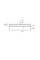
- FIG. 1 is an explanatory diagram showing a configuration of a distance measuring device according to an embodiment of the present invention.
- FIG. 2 is a diagram for explaining a cross-sectional configuration of the distance image sensor.
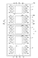
- FIG. 3 is a configuration diagram of the distance image sensor.
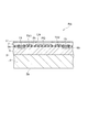
- FIG. 4 is a diagram showing a cross-sectional configuration along the line IV-IV shown in FIG.
- FIG. 5 is a diagram showing a cross-sectional configuration along the line VV shown in FIG.
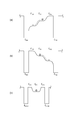
- FIG. 6 is a diagram showing a potential distribution in the vicinity of the second main surface of the semiconductor substrate.
- FIG. 7 is a diagram showing a potential distribution in the vicinity of the second main surface of the semiconductor substrate.
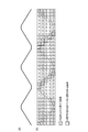
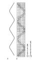
- FIG. 8 is a timing chart of various signals.
- FIG. 1 is an explanatory diagram showing a configuration of a distance measuring device according to an embodiment of the present invention.
- FIG. 2 is a diagram for explaining a cross-sectional configuration of the distance image sensor.
- FIG. 3 is a configuration diagram of
- the second transfer electrode TX2 is provided on the insulating layer 7 and between the photogate electrode PG and the second signal charge collection region 9b.
- the second transfer electrode TX2 is disposed separately from the second signal charge collection region 9b and the photogate electrode PG.
- the second transfer electrode TX2 causes the charge generated in the charge generation region in response to the second transfer signal STX2 to flow into the second signal charge collection region 9b as a signal charge.
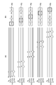
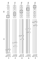
- FIGS. 6 and 7 are diagrams showing the potential distribution in the vicinity of the second main surface of the semiconductor substrate.
- FIG. 6 is a diagram for explaining a signal charge collecting operation (accumulating operation).
- FIG. 7 is a diagram for explaining the operation of discharging unnecessary charges.
- FIGS. 6A and 6B and FIG. 7A show potential distributions in the vicinity of the second main surface 2b of the semiconductor substrate 2 along the line IV-IV shown in FIG.
- FIGS. 6C and 7B show potential distributions in the vicinity of the second main surface 2b of the semiconductor substrate 2 along the line VV shown in FIG.
- the selection unit SEL corresponds to the corresponding distance sensor so as to perform the signal charge collecting operation and the charge collecting operation prior to the signal charge collecting operation for the channels 2ch to 5ch other than the channel 1ch.
- First to third transfer signals STX1, STX2, and STX3 are output to P.
- the charges collected by the collecting operation prior to the signal charge collecting operation are collected in the first signal charge collecting region 9a and the second signal charge collecting region 9b in the same manner as the signal charge.
- the timing at which the reflected light Lr does not enter the distance sensor P constituting the pixels corresponding to the channels 1ch to 5ch is different from the timing at which the signal charges flow into the first and second signal charge collection regions 9a and 9b.
- the calculation unit ART reads a signal from the pixel selected by the selection unit SEL, and calculates the distance to the object OJ for each pixel.
- the arithmetic unit ART has the charge amounts Q 1 and Q 2 based on the signal charge collecting operation and the signal charge collecting operation for each of the distance sensors P constituting the pixels corresponding to the channel channels 1ch to 5ch. The charge amount based on the charge collecting operation prior to the reading is read out.
- the selection unit SEL (control unit CONT) has a timing at which the pulsed light Lp is not emitted from the light source LS prior to the flow of the signal charges into the first and second signal charge collection regions 9a and 9b.
- the first and second transfer signals STX1 and STX2 are output so that charges flow into the first and second signal charge collection regions 9a and 9b, the present invention is not limited to this.
- the selection unit SEL (control unit CONT) performs the first and second signal charge inflows into the first and second signal charge collection regions 9a and 9b and at the timing when the pulsed light Lp is not emitted from the light source LS.
- the first and second transfer signals STX1 and STX2 may be output so that charges flow into the two-signal charge collection regions 9a and 9b.
- the charge generation region in which charge is generated in response to incident light may be configured by a photodiode (for example, a buried photodiode).
Landscapes
- Engineering & Computer Science (AREA)
- Physics & Mathematics (AREA)
- Computer Networks & Wireless Communication (AREA)
- General Physics & Mathematics (AREA)
- Radar, Positioning & Navigation (AREA)
- Remote Sensing (AREA)
- Electromagnetism (AREA)
- Multimedia (AREA)
- Signal Processing (AREA)
- Optical Radar Systems And Details Thereof (AREA)
- Measurement Of Optical Distance (AREA)
- Solid State Image Pick-Up Elements (AREA)
Abstract
Description
第一半導体領域4:厚さ10~1000μm/不純物濃度1×1012~1019cm-3
第二半導体領域5:厚さ1~50μm/不純物濃度1×1012~1015cm-3
第一及び第二信号電荷収集領域9a,9b:厚さ0.1~1μm/不純物濃度1×1018~1020cm-3
不要電荷排出領域11:厚さ0.1~1μm/不純物濃度1×1018~1020cm-3
距離d=(c/2)×(TP×QT2/(QT1+QT2)) ・・・ (1)
すなわち、演算部ARTは、第一及び第二信号電荷収集領域9a,9bに蓄積された信号電荷の電荷量Q1,Q2をそれぞれ読み出し、読み出した電荷量Q1,Q2に基づいて対象物OJまでの距離dを演算する。演算部ARTは、この際、時系列で連続して第一信号電荷収集領域9aと第二信号電荷収集領域9bとに蓄積された信号電荷の合計電荷量QT1,QT2に基づいて対象物OJまでの距離dを演算する。
Claims (2)
- 測距装置であって、
光源から出射されたパルス光の対象物への照射位置を走査する走査部と、
一次元方向に配置されている複数の画素を有し、前記対象物でのパルス光の反射光が入射する受光部と、
前記走査部によるパルス光の照射位置に応じて、信号を読み出す画素を前記複数の画素から選択する選択部と、
前記選択部により選択された画素から信号を読み出し、前記対象物までの距離を演算する演算部と、を備え、
前記複数の画素それぞれは、
入射光に応じて電荷が発生する電荷発生領域と、
前記電荷発生領域からそれぞれ離間して配置され、前記電荷発生領域にて発生した電荷を信号電荷として収集する第一及び第二信号電荷収集領域と、
前記電荷発生領域から離間して配置され、前記電荷発生領域にて発生した電荷を不要電荷として排出する不要電荷排出領域と、
前記第一信号電荷収集領域と前記電荷発生領域との間に配置され、第一転送信号に応じて前記電荷発生領域にて発生した電荷を信号電荷として前記第一信号電荷収集領域に流入させる第一転送電極と、
前記第二信号電荷収集領域と前記電荷発生領域との間に配置され、前記第一転送信号と位相が異なる第二転送信号に応じて前記電荷発生領域にて発生した電荷を信号電荷として前記第二信号電荷収集領域に流入させる第二転送電極と、
前記不要電荷排出領域と前記電荷発生領域との間に配置され、前記第一及び第二転送信号と位相が異なる第三転送信号に応じて前記電荷発生領域にて発生した電荷を不要電荷として前記不要電荷排出領域に流入させる第三転送電極と、を備えており、
前記選択部は、前記走査部によるパルス光の照射位置に応じて、前記複数の画素のうち前記照射位置に対応する画素の前記第一及び第二信号電荷収集領域に信号電荷を流入させるように前記第一転送電極に前記第一転送信号を出力すると共に前記第二転送電極に前記第二転送信号を出力し、前記複数の画素のうち前記照射位置に対応する画素以外の画素の前記不要電荷排出領域に不要電荷を流入させるように前記第三転送電極に前記第三転送信号を出力し、
前記演算部は、前記選択部により選択された画素の前記第一及び第二信号電荷収集領域それぞれに収集された信号電荷の量に対応する信号を読み出し、前記第一信号電荷収集領域に収集された信号電荷の量と前記第二信号電荷収集領域に収集された信号電荷の量との比率に基づいて前記対象物までの距離を演算する。 - 請求項1に記載の測距装置であって、
前記選択部は、選択した画素において、前記第一及び第二信号電荷収集領域へ信号電荷を流入させるタイミングと異なり、かつ、前記光源からパルス光が出射されないタイミングで、前記第一及び第二信号電荷収集領域に電荷を流入させるように前記第一転送電極に前記第一転送信号を出力すると共に前記第二転送電極に前記第二転送信号を出力し、
前記演算部は、前記光源からパルス光が出射されないタイミングで前記第一信号電荷収集領域に収集された電荷の量が減じられた前記第一信号電荷収集領域に収集された信号電荷の量と、前記光源からパルス光が出射されないタイミングで前記第二信号電荷収集領域に収集された電荷の量が減じられた前記第二信号電荷収集領域に収集された信号電荷の量と、の比率に基づいて前記対象物までの距離を演算する。
Priority Applications (5)
| Application Number | Priority Date | Filing Date | Title |
|---|---|---|---|
| KR1020167036922A KR102291769B1 (ko) | 2014-06-09 | 2015-05-28 | 측거 장치 |
| CH01575/16A CH711394B1 (de) | 2014-06-09 | 2015-05-28 | Abstandsmessungsvorrichtung. |
| CN201580030678.7A CN106461781B (zh) | 2014-06-09 | 2015-05-28 | 测距装置 |
| US15/316,935 US11054522B2 (en) | 2014-06-09 | 2015-05-28 | Distance measuring device |
| DE112015002711.4T DE112015002711T5 (de) | 2014-06-09 | 2015-05-28 | Abstandsmessungsvorrichtung |
Applications Claiming Priority (2)
| Application Number | Priority Date | Filing Date | Title |
|---|---|---|---|
| JP2014118623A JP6386798B2 (ja) | 2014-06-09 | 2014-06-09 | 測距装置 |
| JP2014-118623 | 2014-06-09 |
Publications (1)
| Publication Number | Publication Date |
|---|---|
| WO2015190308A1 true WO2015190308A1 (ja) | 2015-12-17 |
Family
ID=54833410
Family Applications (1)
| Application Number | Title | Priority Date | Filing Date |
|---|---|---|---|
| PCT/JP2015/065458 Ceased WO2015190308A1 (ja) | 2014-06-09 | 2015-05-28 | 測距装置 |
Country Status (7)
| Country | Link |
|---|---|
| US (1) | US11054522B2 (ja) |
| JP (1) | JP6386798B2 (ja) |
| KR (1) | KR102291769B1 (ja) |
| CN (1) | CN106461781B (ja) |
| CH (1) | CH711394B1 (ja) |
| DE (1) | DE112015002711T5 (ja) |
| WO (1) | WO2015190308A1 (ja) |
Cited By (1)
| Publication number | Priority date | Publication date | Assignee | Title |
|---|---|---|---|---|
| US10816667B2 (en) | 2016-02-16 | 2020-10-27 | Sony Corporation | Imaging apparatus and imaging control method |
Families Citing this family (8)
| Publication number | Priority date | Publication date | Assignee | Title |
|---|---|---|---|---|
| EP3232224B1 (de) * | 2016-04-12 | 2018-06-13 | Sick Ag | Entfernungsmessender optoelektronischer sensor und verfahren zur erfassung und abstandsbestimmung von objekten |
| JP6659447B2 (ja) | 2016-05-02 | 2020-03-04 | 浜松ホトニクス株式会社 | 距離センサ |
| JP6659448B2 (ja) | 2016-05-02 | 2020-03-04 | 浜松ホトニクス株式会社 | 距離センサ及び距離センサの駆動方法 |
| JP6950276B2 (ja) * | 2017-05-19 | 2021-10-13 | 株式会社デンソーウェーブ | 距離測定装置 |
| JP2020009883A (ja) * | 2018-07-06 | 2020-01-16 | ソニーセミコンダクタソリューションズ株式会社 | 受光素子、測距モジュール、および、電子機器 |
| EP3614174B1 (en) * | 2018-08-21 | 2021-06-23 | Omron Corporation | Distance measuring device and distance measuring method |
| EP4119891A4 (en) * | 2020-03-23 | 2024-05-22 | National University Corporation Shizuoka University | DEVICE FOR ACQUIRING IMAGES BY RANGES |
| JP7464260B2 (ja) * | 2020-03-23 | 2024-04-09 | 国立大学法人静岡大学 | 距離画像センサ |
Citations (6)
| Publication number | Priority date | Publication date | Assignee | Title |
|---|---|---|---|---|
| JP2001194458A (ja) * | 1999-11-05 | 2001-07-19 | Denso Corp | 受光素子、距離測定装置及び距離・画像測定装置 |
| JP2003247809A (ja) * | 2002-02-26 | 2003-09-05 | Olympus Optical Co Ltd | 距離情報入力装置 |
| WO2007026779A1 (ja) * | 2005-08-30 | 2007-03-08 | National University Corporation Shizuoka University | 半導体測距素子及び固体撮像装置 |
| JP2008122223A (ja) * | 2006-11-13 | 2008-05-29 | Suzuki Motor Corp | 距離計測装置 |
| JP2011112385A (ja) * | 2009-11-24 | 2011-06-09 | Hamamatsu Photonics Kk | 距離センサ及び距離画像センサ |
| JP2013050310A (ja) * | 2011-08-30 | 2013-03-14 | Stanley Electric Co Ltd | 距離画像生成装置 |
Family Cites Families (11)
| Publication number | Priority date | Publication date | Assignee | Title |
|---|---|---|---|---|
| US4843565A (en) * | 1987-07-30 | 1989-06-27 | American Electronics, Inc. | Range determination method and apparatus |
| US7352454B2 (en) * | 2000-11-09 | 2008-04-01 | Canesta, Inc. | Methods and devices for improved charge management for three-dimensional and color sensing |
| JP3956991B2 (ja) | 2006-01-20 | 2007-08-08 | ソニー株式会社 | 撮像装置 |
| JP4395150B2 (ja) * | 2006-06-28 | 2010-01-06 | 富士フイルム株式会社 | 距離画像センサ |
| DE102009037596B4 (de) * | 2009-08-14 | 2014-07-24 | Fraunhofer-Gesellschaft zur Förderung der angewandten Forschung e.V. | Pixelstruktur, System und Verfahren zur optischen Abstandsmessung sowie Steuerschaltung für die Pixelstruktur |
| JP5558999B2 (ja) * | 2009-11-24 | 2014-07-23 | 浜松ホトニクス株式会社 | 距離センサ及び距離画像センサ |
| JP5502694B2 (ja) * | 2010-10-12 | 2014-05-28 | 浜松ホトニクス株式会社 | 距離センサ及び距離画像センサ |
| JP5518667B2 (ja) * | 2010-10-12 | 2014-06-11 | 浜松ホトニクス株式会社 | 距離センサ及び距離画像センサ |
| JP6309459B2 (ja) | 2012-02-15 | 2018-04-11 | ヘプタゴン・マイクロ・オプティクス・ピーティーイー・エルティーディーHeptagon Micro Optics Pte.Ltd. | ストライプ照明の飛行時間型カメラ |
| EP2955539B1 (en) * | 2014-06-12 | 2018-08-08 | Delphi International Operations Luxembourg S.à r.l. | Distance measuring device |
| US10890649B2 (en) * | 2016-08-11 | 2021-01-12 | Qualcomm Incorporated | System and method for measuring reference and returned light beams in an optical system |
-
2014
- 2014-06-09 JP JP2014118623A patent/JP6386798B2/ja active Active
-
2015
- 2015-05-28 CH CH01575/16A patent/CH711394B1/de unknown
- 2015-05-28 CN CN201580030678.7A patent/CN106461781B/zh active Active
- 2015-05-28 US US15/316,935 patent/US11054522B2/en active Active
- 2015-05-28 KR KR1020167036922A patent/KR102291769B1/ko active Active
- 2015-05-28 WO PCT/JP2015/065458 patent/WO2015190308A1/ja not_active Ceased
- 2015-05-28 DE DE112015002711.4T patent/DE112015002711T5/de active Pending
Patent Citations (6)
| Publication number | Priority date | Publication date | Assignee | Title |
|---|---|---|---|---|
| JP2001194458A (ja) * | 1999-11-05 | 2001-07-19 | Denso Corp | 受光素子、距離測定装置及び距離・画像測定装置 |
| JP2003247809A (ja) * | 2002-02-26 | 2003-09-05 | Olympus Optical Co Ltd | 距離情報入力装置 |
| WO2007026779A1 (ja) * | 2005-08-30 | 2007-03-08 | National University Corporation Shizuoka University | 半導体測距素子及び固体撮像装置 |
| JP2008122223A (ja) * | 2006-11-13 | 2008-05-29 | Suzuki Motor Corp | 距離計測装置 |
| JP2011112385A (ja) * | 2009-11-24 | 2011-06-09 | Hamamatsu Photonics Kk | 距離センサ及び距離画像センサ |
| JP2013050310A (ja) * | 2011-08-30 | 2013-03-14 | Stanley Electric Co Ltd | 距離画像生成装置 |
Cited By (1)
| Publication number | Priority date | Publication date | Assignee | Title |
|---|---|---|---|---|
| US10816667B2 (en) | 2016-02-16 | 2020-10-27 | Sony Corporation | Imaging apparatus and imaging control method |
Also Published As
| Publication number | Publication date |
|---|---|
| KR102291769B1 (ko) | 2021-08-23 |
| CN106461781A (zh) | 2017-02-22 |
| JP2015232452A (ja) | 2015-12-24 |
| JP6386798B2 (ja) | 2018-09-05 |
| DE112015002711T5 (de) | 2017-02-23 |
| KR20170015941A (ko) | 2017-02-10 |
| US20170115392A1 (en) | 2017-04-27 |
| CH711394B1 (de) | 2018-03-15 |
| US11054522B2 (en) | 2021-07-06 |
| CN106461781B (zh) | 2020-04-14 |
Similar Documents
| Publication | Publication Date | Title |
|---|---|---|
| JP6386798B2 (ja) | 測距装置 | |
| JP6231940B2 (ja) | 測距装置及び測距装置の駆動方法 | |
| JP5518667B2 (ja) | 距離センサ及び距離画像センサ | |
| JP5558999B2 (ja) | 距離センサ及び距離画像センサ | |
| JP6386777B2 (ja) | 距離画像センサ | |
| WO2011065279A1 (ja) | 距離センサ及び距離画像センサ | |
| JP6010425B2 (ja) | 距離センサ及び距離画像センサ | |
| JP5502694B2 (ja) | 距離センサ及び距離画像センサ | |
| JP6315679B2 (ja) | 距離画像センサ | |
| JP2012083213A (ja) | 距離センサ及び距離画像センサ | |
| JP2012083214A (ja) | 距離センサ及び距離画像センサ | |
| JP2012083221A (ja) | 距離センサ及び距離画像センサ | |
| JP5932400B2 (ja) | 距離センサ及び距離画像センサ | |
| JP2012083220A (ja) | 距離センサ及び距離画像センサ | |
| JP2012083219A (ja) | 距離センサ及び距離画像センサ | |
| JP2012083222A (ja) | 距離センサ及び距離画像センサ |
Legal Events
| Date | Code | Title | Description |
|---|---|---|---|
| 121 | Ep: the epo has been informed by wipo that ep was designated in this application |
Ref document number: 15806849 Country of ref document: EP Kind code of ref document: A1 |
|
| WWE | Wipo information: entry into national phase |
Ref document number: 15316935 Country of ref document: US |
|
| WWE | Wipo information: entry into national phase |
Ref document number: 112015002711 Country of ref document: DE |
|
| ENP | Entry into the national phase |
Ref document number: 20167036922 Country of ref document: KR Kind code of ref document: A |
|
| 122 | Ep: pct application non-entry in european phase |
Ref document number: 15806849 Country of ref document: EP Kind code of ref document: A1 |