WO2015186254A1 - 点火装置 - Google Patents
点火装置 Download PDFInfo
- Publication number
- WO2015186254A1 WO2015186254A1 PCT/JP2014/065129 JP2014065129W WO2015186254A1 WO 2015186254 A1 WO2015186254 A1 WO 2015186254A1 JP 2014065129 W JP2014065129 W JP 2014065129W WO 2015186254 A1 WO2015186254 A1 WO 2015186254A1
- Authority
- WO
- WIPO (PCT)
- Prior art keywords
- voltage
- ignition
- switching element
- output
- power supply
- Prior art date
- Legal status (The legal status is an assumption and is not a legal conclusion. Google has not performed a legal analysis and makes no representation as to the accuracy of the status listed.)
- Ceased
Links
Images




Classifications
-
- F—MECHANICAL ENGINEERING; LIGHTING; HEATING; WEAPONS; BLASTING
- F02—COMBUSTION ENGINES; HOT-GAS OR COMBUSTION-PRODUCT ENGINE PLANTS
- F02P—IGNITION, OTHER THAN COMPRESSION IGNITION, FOR INTERNAL-COMBUSTION ENGINES; TESTING OF IGNITION TIMING IN COMPRESSION-IGNITION ENGINES
- F02P1/00—Installations having electric ignition energy generated by magneto- or dynamo- electric generators without subsequent storage
- F02P1/08—Layout of circuits
-
- F—MECHANICAL ENGINEERING; LIGHTING; HEATING; WEAPONS; BLASTING
- F02—COMBUSTION ENGINES; HOT-GAS OR COMBUSTION-PRODUCT ENGINE PLANTS
- F02P—IGNITION, OTHER THAN COMPRESSION IGNITION, FOR INTERNAL-COMBUSTION ENGINES; TESTING OF IGNITION TIMING IN COMPRESSION-IGNITION ENGINES
- F02P3/00—Other installations
- F02P3/06—Other installations having capacitive energy storage
- F02P3/08—Layout of circuits
Definitions
- the present invention relates to an ignition device for igniting an ignition plug of an internal combustion engine.
- an AC-CDI (hereinafter referred to as an ignition device) 10X using the AC output Vac from the exciter coil L0 of the AC generator ACG as a power supply uses a single-wire input type having an inexpensive configuration.
- an ignition device 10 ⁇ / b> X the positive half-wave of the AC output Vac is used to charge the ignition capacitive element (ignition capacitor) C ⁇ b> 0 and supply power to the ignition control circuit 11.
- the power supply to the ignition control circuit 11 is performed by the control power supply circuit 12Xa in FIG. That is, the capacitive element C1X is charged by the AC output Vac via the diode D2X and the resistor R1X, and power is supplied from the capacitive element C1X.
- the voltage Vout of the power supply is limited by the Zener diode ZD1X.
- the current limiting resistor R1X of the control power supply circuit 12Xa it is necessary to reduce the current limiting resistor R1X of the control power supply circuit 12Xa. However, this reduces the impedance of the control power supply circuit 12Xa, so that the charging voltage Vc of the ignition capacitive element C0 decreases.
- the control power supply circuit 12Xb including the bipolar transistor Q1X shown in FIG.
- the base voltage of the bipolar transistor Q1X is the Zener voltage of the Zener diode ZD1X. Therefore, when the power supply voltage Vout exceeds a certain value, the bipolar transistor Q1X is turned off and the bipolar transistor Q1X The current flowing through is interrupted. As a result, when the rotational speed of the internal combustion engine is low, a kickback voltage is generated by the exciter coil L0 and the AC output Vac is increased.
- the charging voltage Vc of the ignition capacitive element C0 may not be sufficient in the low speed region immediately after the start of the internal combustion engine.
- an object of the present invention is to provide an ignition device capable of increasing the charging voltage of the ignition capacitive element when the rotational speed of the internal combustion engine is low.
- An ignition device includes: A first rectifying element that rectifies an AC output from an AC generator driven by an internal combustion engine; An ignition capacitive element charged with an output voltage from the first rectifying element; An ignition switching element that ignites a spark plug provided in the internal combustion engine via an ignition coil by discharging the ignition capacitive element; An ignition control circuit that controls the ignition switching element to be turned on in accordance with the ignition timing of the internal combustion engine; A power supply circuit for supplying power to the ignition control circuit using the AC output, The power supply circuit is A second rectifying element for rectifying the AC output; The output voltage from the second rectifying element is supplied to one end, the output voltage from the second rectifying element is supplied to the control terminal via the first resistor, and the power is supplied from the other end.
- Switching elements of A first capacitive element connected to the other end of the first switching element And a switching element control circuit that reduces the voltage at the control terminal of the first switching element to a fixed voltage when the voltage of the power source becomes equal to or higher than the first voltage.
- the switching element control circuit includes: A second switching element having one end connected to the control terminal of the first switching element and the other end connected to the fixed voltage; A voltage limiting element that limits a voltage between the other end of the first switching element and a control terminal of the second switching element may be included.
- the second switching element is a bipolar transistor;
- the voltage limiting element limits a voltage between the other end of the first switching element and a base of the bipolar transistor to a second voltage;
- the first voltage may be a sum of a base-emitter voltage of the bipolar transistor and the second voltage.
- the voltage limiting element may be a Zener diode, and the second voltage may be a Zener voltage.
- the switching element control circuit may include a second resistor connected between a control terminal of the second switching element and the voltage limiting element.
- the switching element control circuit may include a second capacitor element connected between a control terminal of the second switching element and the fixed voltage.
- the resistance value of the first resistor may be not less than 10 times the impedance when the first switching element is on.
- An ignition device that rectifies an AC output from an AC generator driven by an internal combustion engine; An ignition capacitive element charged with an output voltage from the first rectifying element; An ignition switching element that ignites a spark plug provided in the internal combustion engine via an ignition coil by discharging the ignition capacitive element; An ignition control circuit that controls the ignition switching element to be turned on in accordance with the ignition timing of the internal combustion engine; A power supply circuit for supplying power to the ignition control circuit using the AC output, The power supply circuit is A second rectifying element for rectifying the AC output; A first resistor to which an output voltage from the second rectifying element is supplied to one end; An output voltage from the second rectifying element is supplied to a collector, the other end of the first resistor is connected to a base, and a first NPN bipolar transistor that supplies the power from an emitter; A first capacitive element connected between an emitter of the first NPN bipolar transistor and a fixed voltage; A second NPN bipolar transistor having a collector connected
- the voltage at the control terminal of the first switching element is reduced to a fixed voltage.
- the kickback voltage generated by turning off the first switching element does not affect the voltage at the control terminal of the first switching element.
- the first switching element can be turned off at a higher speed, so that the current flowing through the first switching element can be interrupted at a higher speed.
- the kickback voltage can be further increased. Accordingly, the charging voltage of the ignition capacitive element can be increased when the rotational speed of the internal combustion engine is low.
- FIG. 1 is a circuit diagram showing a schematic configuration of an ignition system according to a first embodiment. It is a circuit diagram which shows schematic structure of the control power supply circuit of FIG. It is a wave form diagram of each signal of the ignition device of FIG. In the control power supply circuit of FIG. 2, the control power supply circuit of FIG. 6B, or the ignition circuit using the control power supply circuit of FIG. 6C, the charging voltage Vc and the rotational speed Ne of the internal combustion engine It is a figure which shows a relationship. It is a circuit diagram which shows schematic structure of the control power supply circuit which concerns on 2nd Embodiment.
- (A) is a circuit diagram which shows schematic structure of the conventional ignition system
- (b) is a circuit diagram which shows schematic structure of the conventional control power supply circuit. It is a wave form chart of each signal of an ignition device using the conventional control power supply circuit of Drawing 6 (c).
- FIG. 1 is a circuit diagram showing a schematic configuration of the ignition system according to the first embodiment.
- This ignition system is used for igniting an internal combustion engine (not shown) for a vehicle such as a motorcycle.
- the ignition system includes an AC generator ACG, a pickup coil 1, an ignition device 10, an ignition coil T0, and a spark plug 2.
- the AC generator ACG is driven by an internal combustion engine to generate power.
- the AC generator ACG has an exciter coil L0 whose one end is grounded, and the generated AC output Vac is output from the other end of the exciter coil L0.
- the AC generator ACG can also generate power by kicking the kick pedal by the user when starting the internal combustion engine.
- the pickup coil 1 detects the rotational position of the crankshaft of the internal combustion engine and outputs a crank position signal representing the rotational position.
- the single-wire input type ignition device 10 uses the AC output Vac from the AC generator ACG (that is, the exciter coil L0) as a power source to ignite the spark plug 2 via the ignition coil T0.
- the ignition coil T0 is also called an ignition coil, and has a primary side coil T01 and a secondary side coil T02.
- the primary coil T01 has one end connected to the ignition device 10 and the other end grounded.
- the secondary coil T02 has one end connected to the spark plug 2 and the other end grounded.
- the spark plug 2 is connected between the secondary coil T02 of the ignition coil T0 and the ground.
- the spark plug 2 is provided in the internal combustion engine and ignites the internal combustion engine.
- the ignition device 10 includes a first rectifier element D1, a third rectifier element D3, an ignition control circuit 11, a control power supply circuit (power supply circuit) 12, an ignition switching element SCR1, and an ignition capacitor element. C0.
- the first rectifying element D1 is a diode and rectifies the AC output Vac from the AC generator ACG.
- an anode is connected to the other end of the exciter coil L0, and a cathode is connected to one end of the ignition capacitive element C0.
- the third rectifying element D3 is a diode, the anode is grounded, and the cathode is connected to the anode of the first rectifying element D1.
- the third rectifying element D3 prevents a negative half wave from the exciter coil L0 from being input to the ignition device 10 and provides a path for a counter electromotive force generated when the ignition capacitive element C0 is discharged.
- the ignition capacitive element C0 is charged with the output voltage from the first rectifying element D1.
- the other end of the ignition capacitive element C0 is connected to one end of the primary coil T01 of the ignition coil T0.
- the voltage at one end of the ignition capacitive element C0 is referred to as a charging voltage Vc.
- the ignition switching element SCR1 is a thyristor, and ignites the ignition plug 2 provided in the internal combustion engine via the ignition coil T0 by discharging the ignition capacitive element C0 when turned on.
- the ignition switching element SCR1 has an anode connected to the cathode of the first rectifying element D1, a cathode grounded, and a control terminal driven by the ignition control circuit 11.
- the ignition control circuit 11 controls the ignition switching element SCR1 to be turned on in accordance with the ignition timing of the internal combustion engine in accordance with the crank position signal supplied from the pickup coil 1.
- the ignition control circuit 11 since the ignition control circuit 11 is configured using a microcomputer, the power consumption is relatively large.
- the control power supply circuit 12 supplies DC power to the ignition control circuit 11 using the AC output Vac from the AC generator ACG (that is, the exciter coil L0). This will be described in more detail below.
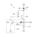
- FIG. 2 is a circuit diagram showing a schematic configuration of the control power supply circuit 12 of FIG.
- the control power supply circuit 12 includes a second rectifier element D2, a first switching element Q1, a first resistor R1, a first capacitor element C1, and a switching element control circuit 121. And having.
- the second rectifier element D2 is a diode and rectifies the AC output Vac supplied to the anode.
- the output voltage from the second rectifying element D2 is supplied to one end of the first resistor R1.
- the first switching element Q1 is a first NPN-type bipolar transistor, and an output voltage from the second rectifying element D2 is supplied to a collector (one end), and the other end of the first resistor R1 is a base (control terminal). ) And supply power to the ignition control circuit 11 from the emitter (the other end). That is, the output voltage from the second rectifier element D2 is also supplied to the base of the first switching element Q1 via the first resistor R1.
- the first capacitive element C1 is connected between the emitter of the first switching element Q1 and the ground voltage (fixed voltage).
- the switching element control circuit 121 reduces the base voltage of the first switching element Q1 to the ground voltage when the voltage Vout of the power supply becomes equal to or higher than the first voltage.
- the switching element control circuit 121 includes a second switching element Q2 and a voltage limiting element ZD1.
- the second switching element Q2 is a second NPN bipolar transistor, and has a collector (one end) connected to the base of the first switching element Q1 and an emitter (the other end) connected to the ground voltage.
- the voltage limiting element ZD1 is a Zener diode, the cathode is connected to the emitter of the first switching element Q1, and the anode is connected to the base (control terminal) of the second switching element Q2. That is, the voltage limiting element ZD1 limits the voltage between the emitter of the first switching element Q1 and the base of the second switching element Q2 to a Zener voltage (second voltage).
- the aforementioned first voltage is the sum of the base-emitter voltage of the second switching element Q2 and the Zener voltage.
- the resistance value of the first resistor R1 is higher than the impedance between the collector and the emitter when the first switching element Q1 is on.
- the resistance value of the first resistor R1 is preferably not less than 10 times the impedance between the collector and the emitter when the first switching element Q1 is on.
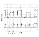
- FIG. 3 is a waveform diagram of each signal of the ignition device 10 of FIG. FIG. 3 shows the charging voltage Vc, the AC output Vac, the power supply voltage Vout, and the input current Iin when the rotational speed of the internal combustion engine is low (for example, 1000 r / min or less).
- the ignition switching element SCR1 is turned on, and the ignition capacitive element C0 is discharged. Therefore, the charging voltage Vc is about 0V.
- the impedance of the control power supply circuit 12 is increased by turning off the first switching element Q1. This is because the resistance value of the first resistor R1 is higher than the impedance when the first switching element Q1 is on. This also contributes to an increase in the AC voltage Vac.
- the voltage Vout of the power supply decreases.
- the second switching element Q2 is turned off.
- FIG. 7 is a waveform diagram of each signal of the ignition device 10X using the conventional control power supply circuit 12Xb of FIG. 6 (c). 7 and 3, the horizontal axis and the vertical axis have the same scale, and the rotational speed of the internal combustion engine is also the same.
- the present inventor has reached the configuration of the control power supply circuit 12 of the present embodiment described above based on such unique knowledge.
- the charging voltage Vc is higher than that of the prior art. This is because, in this embodiment, the AC output Vac is high due to a kickback voltage higher than that of the prior art.
- FIG. 4 shows the charging voltage Vc and the internal combustion in the ignition circuit using the control power supply circuit 12 in FIG. 2, the control power supply circuit 12Xa in FIG. 6B, or the control power supply circuit 12Xb in FIG. It is a figure which shows the relationship with the rotation speed Ne of an engine.
- the charging voltage Vc is higher than that of the control power supply circuits 12Xa and 12Xb of FIGS. 6B and 6C.
- the rotational speed Ne is, for example, 1000 r / min or less.
- the charging voltage Vc can be increased particularly in this range, so that the internal combustion engine can be ignited more reliably than in the prior art when the rotational speed at the start is low.
- the charging voltage Vc of the present embodiment approaches the charging voltage Vc of the control power supply circuits 12Xa and 12Xb in FIGS. However, even in this range, in the present embodiment, the charging voltage Vc is higher than the control power supply circuits 12Xa and 12Xb of FIGS. 6B and 6C.
- the first switching element Q1 when the voltage Vout of the power supply becomes equal to or higher than the first voltage, the voltage at the base of the first switching element Q1 is lowered to the ground voltage. . Therefore, when the rotational speed of the internal combustion engine is low, the kickback voltage generated by turning off the first switching element Q1 does not affect the base voltage of the first switching element Q1. Thus, even if a kickback voltage is generated, the first switching element Q1 can be turned off faster than the prior art of FIG. 6C, so that the current flowing through the first switching element Q1 is cut off at a higher speed. it can. As a result, the kickback voltage can be further increased.
- the charging voltage Vc of the ignition capacitive element C0 can be increased when the rotational speed of the internal combustion engine is low.
- the circuit configuration of the switching element control circuit 121a of the control power supply circuit 12a is different from that of the first embodiment.
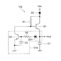
- FIG. 5 is a circuit diagram showing a schematic configuration of the control power supply circuit 12a according to the second embodiment.
- the same reference numerals are given to the components common to FIG. 2, and the differences will be mainly described below.
- the switching element control circuit 121a of the control power supply circuit 12a further includes a second resistor R2 and a second capacitor element C2 in addition to the configuration of the first embodiment of FIG. Prepare.
- the second resistor R2 is connected between the base of the second switching element Q2 and the anode of the voltage limiting element ZD1. Thereby, it can restrict
- the second capacitor element C2 is connected between the base of the second switching element Q2 and the ground voltage. As a result, the voltage at the base of the second switching element Q2 can be maintained, so that the second switching element Q2 once turned on can be more reliably turned on until the voltage Vout of the power source becomes less than the first voltage. Can be kept in. Therefore, since the first switching element Q1 once turned on can be more reliably kept off, the kickback voltage can be prevented from being lowered.
- the charging voltage Vc of the ignition capacitive element C0 can be increased more reliably when the rotational speed of the internal combustion engine is low.
- first to third rectifier elements D1 to D3 are diodes.
- the present invention is not limited to this, and other elements having a rectifier function may be used. .
- first and second switching elements Q1 and Q2 are NPN type bipolar transistors
- the present invention is not limited thereto, and other elements having a switching function may be used.
- the ignition switching element SCR1 is a thyristor
- the present invention is not limited thereto, and other elements such as a transistor having a switching function may be used.
Landscapes
- Engineering & Computer Science (AREA)
- Chemical & Material Sciences (AREA)
- Combustion & Propulsion (AREA)
- Mechanical Engineering (AREA)
- General Engineering & Computer Science (AREA)
- Ignition Installations For Internal Combustion Engines (AREA)
Abstract
点火装置(10)は、点火用スイッチング素子(SCR1)を制御する点火制御回路(11)と、内燃機関により駆動される交流発電機(ACG)からの交流出力(Vac)を用いて点火制御回路(11)に電源を供給する電源供給回路(12)と、を備える。電源供給回路(12)は、交流出力(Vac)を整流する第2の整流素子(D2)と、第2の整流素子(D2)からの出力電圧が一端に供給され、第2の整流素子(D2)からの出力電圧が第1の抵抗(R1)を介して制御端子に供給され、電源を他端から供給する第1のスイッチング素子(Q1)と、第1のスイッチング素子(Q1)の他端に接続された第1の容量素子(C1)と、電源の電圧が第1電圧以上になった場合に、第1のスイッチング素子(Q1)の制御端子の電圧を固定電圧に低下させるスイッチング素子制御回路(121)と、を有する。
Description
本発明は、内燃機関の点火プラグに点火する点火装置に関する。
図6(a)に示すように、交流発電機ACGのエキサイターコイルL0からの交流出力Vacを電源としたAC-CDI(以下、点火装置と称す)10Xにおいて、安価な構成の単線入力式が用いられている(例えば、特許文献1参照)。このような点火装置10Xでは、交流出力Vacの正側の半波を用いて、点火用容量素子(点火用コンデンサ)C0の充電と、点火制御回路11への電源供給とを行っている。
点火制御回路11への電源供給は、図6(b)の制御電源供給回路12Xaにより行われる。即ち、交流出力Vacにより、ダイオードD2X及び抵抗R1Xを介して容量素子C1Xが充電され、容量素子C1Xから電源が供給される。電源の電圧Voutは、ツェナーダイオードZD1Xにより制限される。ここで、点火制御回路11の消費電力が大きい場合に対応するには、制御電源供給回路12Xaの電流制限抵抗R1Xを小さくする必要がある。しかし、これにより制御電源供給回路12Xaのインピーダンスが低くなるため、点火用容量素子C0の充電電圧Vcが低下してしまう。
点火用容量素子C0の充電電圧Vcの低下を防止するためには、図6(c)に示すバイポーラトランジスタQ1Xを備える制御電源供給回路12Xbの使用が考えられる。この制御電源供給回路12Xbでは、バイポーラトランジスタQ1Xのベース電圧はツェナーダイオードZD1Xのツェナー電圧になっているので、電源の電圧Voutが一定値以上になった時、バイポーラトランジスタQ1Xはオフし、バイポーラトランジスタQ1Xに流れる電流が遮断される。これにより、内燃機関の回転数が低い時には、エキサイターコイルL0によるキックバック電圧が発生して交流出力Vacが高くなる。加えて、バイポーラトランジスタQ1Xがオフすると、制御電源供給回路12Xbのインピーダンスが高くなるので、充電電圧Vcを高くできる。従って、点火制御回路11の消費電力が大きい場合にも、点火用容量素子C0の充電電圧Vcの低下を防止できる。
しかしながら、図6(c)の制御電源供給回路12Xbを用いても、内燃機関の始動直後の低回転数領域において、点火用容量素子C0の充電電圧Vcが十分ではない場合がある。
そこで、本発明は、内燃機関の回転数が低い時に点火用容量素子の充電電圧を高くできる点火装置を提供することを目的とする。
本発明の一態様に係る点火装置は、
内燃機関により駆動される交流発電機からの交流出力を整流する第1の整流素子と、
前記第1の整流素子からの出力電圧で充電される点火用容量素子と、
前記点火用容量素子を放電させることにより、点火コイルを介して、前記内燃機関に設けられた点火プラグに点火する点火用スイッチング素子と、
前記内燃機関の点火タイミングに合わせて前記点火用スイッチング素子をオンに制御する点火制御回路と、
前記交流出力を用いて前記点火制御回路に電源を供給する電源供給回路と、を備え、
前記電源供給回路は、
前記交流出力を整流する第2の整流素子と、
前記第2の整流素子からの出力電圧が一端に供給され、前記第2の整流素子からの出力電圧が第1の抵抗を介して制御端子に供給され、前記電源を他端から供給する第1のスイッチング素子と、
前記第1のスイッチング素子の他端に接続された第1の容量素子と、
前記電源の電圧が第1電圧以上になった場合に、前記第1のスイッチング素子の制御端子の電圧を固定電圧に低下させるスイッチング素子制御回路と、を有する。
内燃機関により駆動される交流発電機からの交流出力を整流する第1の整流素子と、
前記第1の整流素子からの出力電圧で充電される点火用容量素子と、
前記点火用容量素子を放電させることにより、点火コイルを介して、前記内燃機関に設けられた点火プラグに点火する点火用スイッチング素子と、
前記内燃機関の点火タイミングに合わせて前記点火用スイッチング素子をオンに制御する点火制御回路と、
前記交流出力を用いて前記点火制御回路に電源を供給する電源供給回路と、を備え、
前記電源供給回路は、
前記交流出力を整流する第2の整流素子と、
前記第2の整流素子からの出力電圧が一端に供給され、前記第2の整流素子からの出力電圧が第1の抵抗を介して制御端子に供給され、前記電源を他端から供給する第1のスイッチング素子と、
前記第1のスイッチング素子の他端に接続された第1の容量素子と、
前記電源の電圧が第1電圧以上になった場合に、前記第1のスイッチング素子の制御端子の電圧を固定電圧に低下させるスイッチング素子制御回路と、を有する。
また、前記点火装置において、
前記スイッチング素子制御回路は、
一端が前記第1のスイッチング素子の制御端子に接続され、他端が前記固定電圧に接続された第2のスイッチング素子と、
前記第1のスイッチング素子の他端と前記第2のスイッチング素子の制御端子との間の電圧を制限する電圧制限素子と、を有してもよい。
前記スイッチング素子制御回路は、
一端が前記第1のスイッチング素子の制御端子に接続され、他端が前記固定電圧に接続された第2のスイッチング素子と、
前記第1のスイッチング素子の他端と前記第2のスイッチング素子の制御端子との間の電圧を制限する電圧制限素子と、を有してもよい。
また、前記点火装置において、
前記第2のスイッチング素子は、バイポーラトランジスタであり、
前記電圧制限素子は、前記第1のスイッチング素子の他端と前記バイポーラトランジスタのベースとの間の電圧を第2電圧に制限し、
前記第1電圧は、前記バイポーラトランジスタのベース・エミッタ間電圧と前記第2電圧との和であってもよい。
前記第2のスイッチング素子は、バイポーラトランジスタであり、
前記電圧制限素子は、前記第1のスイッチング素子の他端と前記バイポーラトランジスタのベースとの間の電圧を第2電圧に制限し、
前記第1電圧は、前記バイポーラトランジスタのベース・エミッタ間電圧と前記第2電圧との和であってもよい。
また、前記点火装置において、
前記電圧制限素子はツェナーダイオードであり、前記第2電圧はツェナー電圧であってもよい。
前記電圧制限素子はツェナーダイオードであり、前記第2電圧はツェナー電圧であってもよい。
また、前記点火装置において、
前記スイッチング素子制御回路は、前記第2のスイッチング素子の制御端子と前記電圧制限素子との間に接続された第2の抵抗を有してもよい。
前記スイッチング素子制御回路は、前記第2のスイッチング素子の制御端子と前記電圧制限素子との間に接続された第2の抵抗を有してもよい。
また、前記点火装置において、
前記スイッチング素子制御回路は、前記第2のスイッチング素子の制御端子と前記固定電圧との間に接続された第2の容量素子を有してもよい。
前記スイッチング素子制御回路は、前記第2のスイッチング素子の制御端子と前記固定電圧との間に接続された第2の容量素子を有してもよい。
また、前記点火装置において、
前記第1の抵抗の抵抗値は、前記第1のスイッチング素子のオン時のインピーダンスの10倍以上であってもよい。
前記第1の抵抗の抵抗値は、前記第1のスイッチング素子のオン時のインピーダンスの10倍以上であってもよい。
本発明の他の一態様に係る点火装置は、
内燃機関により駆動される交流発電機からの交流出力を整流する第1の整流素子と、
前記第1の整流素子からの出力電圧で充電される点火用容量素子と、
前記点火用容量素子を放電させることにより、点火コイルを介して、前記内燃機関に設けられた点火プラグに点火する点火用スイッチング素子と、
前記内燃機関の点火タイミングに合わせて前記点火用スイッチング素子をオンに制御する点火制御回路と、
前記交流出力を用いて前記点火制御回路に電源を供給する電源供給回路と、を備え、
前記電源供給回路は、
前記交流出力を整流する第2の整流素子と、
前記第2の整流素子からの出力電圧が一端に供給される第1の抵抗と、
前記第2の整流素子からの出力電圧がコレクタに供給され、前記第1の抵抗の他端がベースに接続され、前記電源をエミッタから供給する第1のNPN型バイポーラトランジスタと、
前記第1のNPN型バイポーラトランジスタのエミッタと固定電圧との間に接続された第1の容量素子と、
コレクタが前記第1のNPN型バイポーラトランジスタのベースに接続され、エミッタが前記固定電圧に接続された第2のNPN型バイポーラトランジスタと、
前記第1のNPN型バイポーラトランジスタのエミッタと前記第2のNPN型バイポーラトランジスタのベースとの間に接続されたツェナーダイオードと、を有する。
内燃機関により駆動される交流発電機からの交流出力を整流する第1の整流素子と、
前記第1の整流素子からの出力電圧で充電される点火用容量素子と、
前記点火用容量素子を放電させることにより、点火コイルを介して、前記内燃機関に設けられた点火プラグに点火する点火用スイッチング素子と、
前記内燃機関の点火タイミングに合わせて前記点火用スイッチング素子をオンに制御する点火制御回路と、
前記交流出力を用いて前記点火制御回路に電源を供給する電源供給回路と、を備え、
前記電源供給回路は、
前記交流出力を整流する第2の整流素子と、
前記第2の整流素子からの出力電圧が一端に供給される第1の抵抗と、
前記第2の整流素子からの出力電圧がコレクタに供給され、前記第1の抵抗の他端がベースに接続され、前記電源をエミッタから供給する第1のNPN型バイポーラトランジスタと、
前記第1のNPN型バイポーラトランジスタのエミッタと固定電圧との間に接続された第1の容量素子と、
コレクタが前記第1のNPN型バイポーラトランジスタのベースに接続され、エミッタが前記固定電圧に接続された第2のNPN型バイポーラトランジスタと、
前記第1のNPN型バイポーラトランジスタのエミッタと前記第2のNPN型バイポーラトランジスタのベースとの間に接続されたツェナーダイオードと、を有する。
本発明によれば、電源の電圧が第1電圧以上になった場合に第1のスイッチング素子の制御端子の電圧を固定電圧に低下させるようにしているので、内燃機関の回転数が低い時、第1のスイッチング素子がオフすることで発生したキックバック電圧は、第1のスイッチング素子の制御端子の電圧に影響を及ぼさない。これにより、キックバック電圧が発生しても第1のスイッチング素子をより高速にオフさせることができるため、第1のスイッチング素子に流れる電流をより高速に遮断できる。その結果、キックバック電圧をより高くできる。
従って、内燃機関の回転数が低い時に点火用容量素子の充電電圧を高くできる。
従って、内燃機関の回転数が低い時に点火用容量素子の充電電圧を高くできる。
以下に、図面を参照して本発明の実施形態について説明する。これらの実施形態は、本発明を限定するものではない。
(第1の実施形態)
図1は、第1の実施形態に係る点火システムの概略構成を示す回路図である。この点火システムは、例えば自動二輪車等の車両用の内燃機関(図示せず)に点火するために用いられる。図1に示すように、点火システムは、交流発電機ACGと、ピックアップコイル1と、点火装置10と、点火コイルT0と、点火プラグ2と、を備える。
図1は、第1の実施形態に係る点火システムの概略構成を示す回路図である。この点火システムは、例えば自動二輪車等の車両用の内燃機関(図示せず)に点火するために用いられる。図1に示すように、点火システムは、交流発電機ACGと、ピックアップコイル1と、点火装置10と、点火コイルT0と、点火プラグ2と、を備える。
交流発電機ACGは、内燃機関により駆動されて発電する。交流発電機ACGは、一端が接地されたエキサイターコイルL0を有しており、発電された交流出力VacがエキサイターコイルL0の他端から出力される。なお、交流発電機ACGは、内燃機関の始動時には、ユーザによるキックペダルのキックにより発電することもできる。
ピックアップコイル1は、内燃機関のクランク軸の回転位置を検出して、その回転位置を表すクランク位置信号を出力する。
単線入力式の点火装置10は、交流発電機ACG(即ち、エキサイターコイルL0)からの交流出力Vacを電源として、点火コイルT0を介して点火プラグ2に点火する。
点火コイルT0は、イグニッションコイルとも称され、一次側コイルT01と、二次側コイルT02と、を有する。一次側コイルT01は、一端が点火装置10に接続され、他端が接地されている。二次側コイルT02は、一端が点火プラグ2に接続され、他端が接地されている。
点火プラグ2は、点火コイルT0の二次側コイルT02と接地との間に接続されている。点火プラグ2は、内燃機関に設けられ、内燃機関に点火する。
点火装置10は、第1の整流素子D1と、第3の整流素子D3と、点火制御回路11と、制御電源供給回路(電源供給回路)12と、点火用スイッチング素子SCR1と、点火用容量素子C0と、を備える。
第1の整流素子D1は、ダイオードであり、交流発電機ACGからの交流出力Vacを整流する。第1の整流素子D1は、エキサイターコイルL0の他端にアノードが接続され、点火用容量素子C0の一端にカソードが接続されている。
第3の整流素子D3は、ダイオードであり、アノードが接地され、カソードが第1の整流素子D1のアノードに接続されている。第3の整流素子D3は、エキサイターコイルL0から負側の半波が点火装置10に入力されないようにすると共に、点火用容量素子C0の放電時に発生する逆起電力の経路となる。
点火用容量素子C0は、第1の整流素子D1からの出力電圧で充電される。点火用容量素子C0は、他端が点火コイルT0の一次側コイルT01の一端に接続されている。点火用容量素子C0の一端の電圧を充電電圧Vcと称す。
点火用スイッチング素子SCR1は、サイリスタであり、オン時に点火用容量素子C0を放電させることにより、点火コイルT0を介して、内燃機関に設けられた点火プラグ2に点火する。点火用スイッチング素子SCR1は、アノードが第1の整流素子D1のカソードに接続され、カソードが接地され、制御端子が点火制御回路11により駆動される。
点火制御回路11は、ピックアップコイル1から供給されたクランク位置信号に応じて、内燃機関の点火タイミングに合わせて点火用スイッチング素子SCR1をオンに制御する。本実施形態では、点火制御回路11はマイコンを用いて構成されているため、消費電力が比較的大きい。
制御電源供給回路12は、交流発電機ACG(即ち、エキサイターコイルL0)からの交流出力Vacを用いて点火制御回路11に直流電源を供給する。以下に、より詳しく説明する。
図2は、図1の制御電源供給回路12の概略構成を示す回路図である。図2に示すように、制御電源供給回路12は、第2の整流素子D2と、第1のスイッチング素子Q1と、第1の抵抗R1と、第1の容量素子C1と、スイッチング素子制御回路121と、を有する。
第2の整流素子D2は、ダイオードであり、アノードに供給された交流出力Vacを整流する。第1の抵抗R1は、第2の整流素子D2からの出力電圧が一端に供給される。
第1のスイッチング素子Q1は、第1のNPN型バイポーラトランジスタであり、第2の整流素子D2からの出力電圧がコレクタ(一端)に供給され、第1の抵抗R1の他端がベース(制御端子)に接続され、電源をエミッタ(他端)から点火制御回路11に供給する。つまり、第2の整流素子D2からの出力電圧は、第1の抵抗R1を介して第1のスイッチング素子Q1のベースにも供給される。
第1の容量素子C1は、第1のスイッチング素子Q1のエミッタと接地電圧(固定電圧)との間に接続されている。
スイッチング素子制御回路121は、電源の電圧Voutが第1電圧以上になった場合に、第1のスイッチング素子Q1のベースの電圧を接地電圧に低下させる。具体的には、スイッチング素子制御回路121は、第2のスイッチング素子Q2と、電圧制限素子ZD1と、を有する。
第2のスイッチング素子Q2は、第2のNPN型バイポーラトランジスタであり、コレクタ(一端)が第1のスイッチング素子Q1のベースに接続され、エミッタ(他端)が接地電圧に接続されている。
電圧制限素子ZD1は、ツェナーダイオードであり、カソードが第1のスイッチング素子Q1のエミッタに接続され、アノードが第2のスイッチング素子Q2のベース(制御端子)に接続されている。つまり、電圧制限素子ZD1は、第1のスイッチング素子Q1のエミッタと第2のスイッチング素子Q2のベースとの間の電圧をツェナー電圧(第2電圧)に制限する。
前述の第1電圧は、第2のスイッチング素子Q2のベース・エミッタ間電圧とツェナー電圧との和である。
第1の抵抗R1の抵抗値は、第1のスイッチング素子Q1のオン時のコレクタ・エミッタ間のインピーダンスより高い。第1の抵抗R1の抵抗値は、第1のスイッチング素子Q1のオン時のコレクタ・エミッタ間のインピーダンスの10倍以上であることが好ましい。
次に、図3を参照して点火装置10の動作を説明する。
図3は、図1の点火装置10の各信号の波形図である。図3は、内燃機関の回転数が低い場合(例えば、1000r/min以下)について、充電電圧Vc、交流出力Vac、電源の電圧Vout、及び、入力電流Iinを示している。
時刻t1において、点火用スイッチング素子SCR1がオンして、点火用容量素子C0は放電する。よって、充電電圧Vcは約0Vになる。
次に、時刻t2において、交流出力Vacが0Vから上昇すると、第1のスイッチング素子Q1がオンになり、入力電流Iinが第2の整流素子D2及び第1のスイッチング素子Q1を流れる。これにより、第1の容量素子C1が充電され、電源の電圧Voutが上昇する。
次に、時刻t3において、電源の電圧Voutが第1電圧以上になると、第2のスイッチング素子Q2がオンして、第1のスイッチング素子Q1のベースの電圧は接地電圧に低下する。これにより、第1のスイッチング素子Q1はオフになり、そのコレクタ電流が遮断される。
コレクタ電流が遮断されると、時刻t3以降、エキサイターコイルL0により誘導性のキックバック電圧が発生する。よって、交流出力Vacが上昇するため、充電電圧Vcも上昇する。
このとき、キックバック電圧により交流出力Vacが上昇しても、第2のスイッチング素子Q2がオンしているため、第1のスイッチング素子Q1のベースの電圧はほぼ接地電圧に保たれている。よって、キックバック電圧の発生は、第1のスイッチング素子Q1のオフには影響を与えない。
また、第1のスイッチング素子Q1がオフすることにより、制御電源供給回路12のインピーダンスが高くなる。第1の抵抗R1の抵抗値は、第1のスイッチング素子Q1のオン時のインピーダンスより高いためである。このことも、交流電圧Vacの上昇に寄与する。
この後、電源の電圧Voutは低下していく。電源の電圧Voutが第1電圧未満になると、第2のスイッチング素子Q2はオフになる。
次に、時刻t4において、交流出力Vacが再び上昇すると、第1のスイッチング素子Q1がオンになり、再び電源の電圧Voutが上昇する。
時刻t4以降の動作も、時刻t2から時刻t4までの動作と同様である。
時刻t4以降の動作も、時刻t2から時刻t4までの動作と同様である。
ここで、本発明者が独自に知得した、図6(c)の従来の制御電源供給回路12Xbを用いた点火装置10Xでは、キックバック電圧を十分に高くできないため、交流出力Vacを十分に高くできないことについて説明する。
図7は、図6(c)の従来の制御電源供給回路12Xbを用いた点火装置10Xの各信号の波形図である。図7と図3において、横軸及び縦軸のスケールは同一であり、内燃機関の回転数も同一である。
図7において、時刻t4X以降、電源の電圧Voutが上昇すると、時刻t5XにおいてバイポーラトランジスタQ1Xがオフするため、キックバック電圧が発生し、交流出力Vacが上昇する。交流出力Vacの上昇により、ツェナーダイオードZD1Xに流れる電流が増加する。これにより、ツェナーダイオードZD1Xのツェナー電圧が高くなるため、バイポーラトランジスタQ1Xが再び弱くオンしてしまう。よって、バイポーラトランジスタQ1Xに再び電流が流れて電源の電圧Voutが更に上昇するため、バイポーラトランジスタQ1Xは再度オフになる。このような動作を繰り返すため、バイポーラトランジスタQ1Xがオフする速さは遅くなる。即ち、入力電流Iinは緩やかに減少する。従って、バイポーラトランジスタQ1Xに流れる電流を高速に遮断できないので、誘導性のキックバック電圧を十分に高くできない。
本発明者は、このような独自の知得に基づいて、上述した本実施形態の制御電源供給回路12の構成に至った。
図3及び図7を比較すると、本実施形態では、充電電圧Vcが従来技術よりも高くなっていることが分かる。この理由は、本実施形態では、従来技術よりも高いキックバック電圧によって交流出力Vacが高くなっているためである。
図4は、図2の制御電源供給回路12、図6(b)の制御電源供給回路12Xa、又は、図6(c)の制御電源供給回路12Xbを用いた点火回路における、充電電圧Vcと内燃機関の回転数Neとの関係を示す図である。
図4において、回転数Neが2000r/min以下の範囲では、キックバック電圧による交流出力Vacの上昇と、第1のスイッチング素子Q1がオフしてインピーダンスが高くなることによる交流出力Vacの上昇との両方が生じている。従って、この範囲において、本実施形態では、図6(b),(c)の制御電源供給回路12Xa,12Xbよりも充電電圧Vcが高くなっている。
内燃機関のキックスタート時からアイドリング時の始動時においては、回転数Neは、例えば1000r/min以下である。本実施形態では、特にこの範囲において充電電圧Vcを高くできるため、始動時の回転数が低い時に、従来技術よりも確実に内燃機関に着火できる。
回転数Neが2000r/minより高い範囲では、回転数Neが高くなるほどエキサイターコイルL0の特性によりキックバック電圧が低くなる。そのため、キックバック電圧による交流出力Vacの上昇は小さくなり、インピーダンスが高くなることによる交流出力Vacの上昇が支配的になる。従って、回転数Neが高くなるほど、本実施形態の充電電圧Vcは、図6(b),(c)の制御電源供給回路12Xa,12Xbの充電電圧Vcに近づいていく。しかし、この範囲においても、本実施形態では、図6(b),(c)の制御電源供給回路12Xa,12Xbよりも充電電圧Vcが高くなっている。
以上で説明したように、第1の実施形態によれば、電源の電圧Voutが第1電圧以上になった場合に第1のスイッチング素子Q1のベースの電圧を接地電圧に低下させるようにしている。よって、内燃機関の回転数が低い時、第1のスイッチング素子Q1がオフすることで発生したキックバック電圧は、第1のスイッチング素子Q1のベースの電圧に影響を及ぼさない。これにより、キックバック電圧が発生しても第1のスイッチング素子Q1を図6(c)の従来技術より高速にオフさせることができるため、第1のスイッチング素子Q1に流れる電流をより高速に遮断できる。その結果、キックバック電圧をより高くできる。
従って、内燃機関の回転数が低い時に点火用容量素子C0の充電電圧Vcを高くできる。
(第2の実施形態)
第2の実施形態では、制御電源供給回路12aのスイッチング素子制御回路121aの回路構成が第1の実施形態と異なる。
第2の実施形態では、制御電源供給回路12aのスイッチング素子制御回路121aの回路構成が第1の実施形態と異なる。
図5は、第2の実施形態に係る制御電源供給回路12aの概略構成を示す回路図である。図5では、図2と共通する構成部分には同一の符号を付しており、以下では相違点を中心に説明する。
図5に示すように、制御電源供給回路12aのスイッチング素子制御回路121aは、図2の第1の実施形態の構成に加え、第2の抵抗R2と、第2の容量素子C2と、を更に備える。
第2の抵抗R2は、第2のスイッチング素子Q2のベースと電圧制限素子ZD1のアノードとの間に接続されている。これにより、第2のスイッチング素子Q2のベース電流が大きくなり過ぎないように制限でき、制御電源供給回路12aの信頼性を高めることができる。
第2の容量素子C2は、第2のスイッチング素子Q2のベースと接地電圧との間に接続されている。これにより、第2のスイッチング素子Q2のベースの電圧を保持できるため、一旦オンになった第2のスイッチング素子Q2を、電源の電圧Voutが第1電圧未満になるまでの間、より確実にオンに保つことができる。よって、一旦オンになった第1のスイッチング素子Q1を、より確実にオフに保つことができるので、キックバック電圧を低下させることがないようにできる。
従って、より確実に、内燃機関の回転数が低い時に点火用容量素子C0の充電電圧Vcを高くできる。
なお、第1及び第2の実施形態では、第1から第3の整流素子D1~D3はダイオードである一例について説明したが、これに限らず、整流機能を有している他の素子でもよい。
また、第1及び第2のスイッチング素子Q1,Q2はNPN型バイポーラトランジスタである一例について説明したが、これに限らず、スイッチング機能を有している他の素子でもよい。
また、点火用スイッチング素子SCR1はサイリスタである一例について説明したが、これに限らず、スイッチング機能を有しているトランジスタ等の他の素子でもよい。
本発明の態様は、上述した個々の実施形態に限定されるものではなく、当業者が想到しうる種々の変形も含むものであり、本発明の効果も上述した内容に限定されない。すなわち、特許請求の範囲に規定された内容およびその均等物から導き出される本発明の概念的な思想と趣旨を逸脱しない範囲で種々の追加、変更および部分的削除が可能である。
ACG 交流発電機
L0 エキサイターコイル
1 ピックアップコイル
2 点火プラグ
T0 点火コイル
10 点火装置
11 点火制御回路
12,12a 制御電源供給回路(電源供給回路)
121,121a スイッチング素子制御回路
C0 点火用容量素子
SCR1 点火用スイッチング素子
D1 第1の整流素子
D2 第2の整流素子
D3 第3の整流素子
Q1 第1のスイッチング素子
Q2 第2のスイッチング素子
R1 第1の抵抗
R2 第2の抵抗
C1 第1の容量素子
C2 第2の容量素子
ZD1 電圧制限素子
L0 エキサイターコイル
1 ピックアップコイル
2 点火プラグ
T0 点火コイル
10 点火装置
11 点火制御回路
12,12a 制御電源供給回路(電源供給回路)
121,121a スイッチング素子制御回路
C0 点火用容量素子
SCR1 点火用スイッチング素子
D1 第1の整流素子
D2 第2の整流素子
D3 第3の整流素子
Q1 第1のスイッチング素子
Q2 第2のスイッチング素子
R1 第1の抵抗
R2 第2の抵抗
C1 第1の容量素子
C2 第2の容量素子
ZD1 電圧制限素子
Claims (8)
- 内燃機関により駆動される交流発電機からの交流出力を整流する第1の整流素子と、
前記第1の整流素子からの出力電圧で充電される点火用容量素子と、
前記点火用容量素子を放電させることにより、点火コイルを介して、前記内燃機関に設けられた点火プラグに点火する点火用スイッチング素子と、
前記内燃機関の点火タイミングに合わせて前記点火用スイッチング素子をオンに制御する点火制御回路と、
前記交流出力を用いて前記点火制御回路に電源を供給する電源供給回路と、を備え、
前記電源供給回路は、
前記交流出力を整流する第2の整流素子と、
前記第2の整流素子からの出力電圧が一端に供給され、前記第2の整流素子からの出力電圧が第1の抵抗を介して制御端子に供給され、前記電源を他端から供給する第1のスイッチング素子と、
前記第1のスイッチング素子の他端に接続された第1の容量素子と、
前記電源の電圧が第1電圧以上になった場合に、前記第1のスイッチング素子の制御端子の電圧を固定電圧に低下させるスイッチング素子制御回路と、を有する、ことを特徴とする点火装置。 - 前記スイッチング素子制御回路は、
一端が前記第1のスイッチング素子の制御端子に接続され、他端が前記固定電圧に接続された第2のスイッチング素子と、
前記第1のスイッチング素子の他端と前記第2のスイッチング素子の制御端子との間の電圧を制限する電圧制限素子と、を有する、ことを特徴とする請求項1に記載の点火装置。 - 前記第2のスイッチング素子は、バイポーラトランジスタであり、
前記電圧制限素子は、前記第1のスイッチング素子の他端と前記バイポーラトランジスタのベースとの間の電圧を第2電圧に制限し、
前記第1電圧は、前記バイポーラトランジスタのベース・エミッタ間電圧と前記第2電圧との和である、ことを特徴とする請求項2に記載の点火装置。 - 前記電圧制限素子はツェナーダイオードであり、前記第2電圧はツェナー電圧である、ことを特徴とする請求項3に記載の点火装置。
- 前記スイッチング素子制御回路は、前記第2のスイッチング素子の制御端子と前記電圧制限素子との間に接続された第2の抵抗を有する、ことを特徴とする請求項2から請求項4の何れかに記載の点火装置。
- 前記スイッチング素子制御回路は、前記第2のスイッチング素子の制御端子と前記固定電圧との間に接続された第2の容量素子を有する、ことを特徴とする請求項2から請求項5の何れかに記載の点火装置。
- 前記第1の抵抗の抵抗値は、前記第1のスイッチング素子のオン時のインピーダンスの10倍以上である、ことを特徴とする請求項1から請求項6の何れかに記載の点火装置。
- 内燃機関により駆動される交流発電機からの交流出力を整流する第1の整流素子と、
前記第1の整流素子からの出力電圧で充電される点火用容量素子と、
前記点火用容量素子を放電させることにより、点火コイルを介して、前記内燃機関に設けられた点火プラグに点火する点火用スイッチング素子と、
前記内燃機関の点火タイミングに合わせて前記点火用スイッチング素子をオンに制御する点火制御回路と、
前記交流出力を用いて前記点火制御回路に電源を供給する電源供給回路と、を備え、
前記電源供給回路は、
前記交流出力を整流する第2の整流素子と、
前記第2の整流素子からの出力電圧が一端に供給される第1の抵抗と、
前記第2の整流素子からの出力電圧がコレクタに供給され、前記第1の抵抗の他端がベースに接続され、前記電源をエミッタから供給する第1のNPN型バイポーラトランジスタと、
前記第1のNPN型バイポーラトランジスタのエミッタと固定電圧との間に接続された第1の容量素子と、
コレクタが前記第1のNPN型バイポーラトランジスタのベースに接続され、エミッタが前記固定電圧に接続された第2のNPN型バイポーラトランジスタと、
前記第1のNPN型バイポーラトランジスタのエミッタと前記第2のNPN型バイポーラトランジスタのベースとの間に接続されたツェナーダイオードと、を有する、ことを特徴とする点火装置。
Priority Applications (3)
| Application Number | Priority Date | Filing Date | Title |
|---|---|---|---|
| JP2015511851A JP5912208B1 (ja) | 2014-06-06 | 2014-06-06 | 点火装置 |
| PCT/JP2014/065129 WO2015186254A1 (ja) | 2014-06-06 | 2014-06-06 | 点火装置 |
| CN201480002871.5A CN106170621B (zh) | 2014-06-06 | 2014-06-06 | 点火装置 |
Applications Claiming Priority (1)
| Application Number | Priority Date | Filing Date | Title |
|---|---|---|---|
| PCT/JP2014/065129 WO2015186254A1 (ja) | 2014-06-06 | 2014-06-06 | 点火装置 |
Publications (1)
| Publication Number | Publication Date |
|---|---|
| WO2015186254A1 true WO2015186254A1 (ja) | 2015-12-10 |
Family
ID=54766346
Family Applications (1)
| Application Number | Title | Priority Date | Filing Date |
|---|---|---|---|
| PCT/JP2014/065129 Ceased WO2015186254A1 (ja) | 2014-06-06 | 2014-06-06 | 点火装置 |
Country Status (3)
| Country | Link |
|---|---|
| JP (1) | JP5912208B1 (ja) |
| CN (1) | CN106170621B (ja) |
| WO (1) | WO2015186254A1 (ja) |
Families Citing this family (1)
| Publication number | Priority date | Publication date | Assignee | Title |
|---|---|---|---|---|
| US10648442B2 (en) * | 2018-10-15 | 2020-05-12 | Semiconductor Components Industries, Llc | Circuit and method for coil current control |
Citations (3)
| Publication number | Priority date | Publication date | Assignee | Title |
|---|---|---|---|---|
| JPS6210471A (ja) * | 1985-07-08 | 1987-01-19 | Nippon Denso Co Ltd | 内燃機関用無接点点火装置 |
| JPH03164568A (ja) * | 1989-11-21 | 1991-07-16 | Kokusan Denki Co Ltd | コンデンサ放電式内燃機関用点火装置 |
| JPH0566269U (ja) * | 1992-08-10 | 1993-09-03 | 国産電機株式会社 | 内燃機関用点火装置 |
Family Cites Families (3)
| Publication number | Priority date | Publication date | Assignee | Title |
|---|---|---|---|---|
| JP2009150378A (ja) * | 2007-10-09 | 2009-07-09 | Denso Corp | 点火装置 |
| JP5517686B2 (ja) * | 2010-03-19 | 2014-06-11 | 株式会社ケーヒン | 内燃機関用点火装置 |
| CN102852692B (zh) * | 2011-07-01 | 2017-03-01 | 伍德沃德公司 | 用于具有电流模式控制和故障容差检测的ac点火系统的多路复用驱动电路 |
-
2014
- 2014-06-06 JP JP2015511851A patent/JP5912208B1/ja active Active
- 2014-06-06 CN CN201480002871.5A patent/CN106170621B/zh active Active
- 2014-06-06 WO PCT/JP2014/065129 patent/WO2015186254A1/ja not_active Ceased
Patent Citations (3)
| Publication number | Priority date | Publication date | Assignee | Title |
|---|---|---|---|---|
| JPS6210471A (ja) * | 1985-07-08 | 1987-01-19 | Nippon Denso Co Ltd | 内燃機関用無接点点火装置 |
| JPH03164568A (ja) * | 1989-11-21 | 1991-07-16 | Kokusan Denki Co Ltd | コンデンサ放電式内燃機関用点火装置 |
| JPH0566269U (ja) * | 1992-08-10 | 1993-09-03 | 国産電機株式会社 | 内燃機関用点火装置 |
Also Published As
| Publication number | Publication date |
|---|---|
| CN106170621A (zh) | 2016-11-30 |
| CN106170621B (zh) | 2017-06-23 |
| JP5912208B1 (ja) | 2016-04-27 |
| JPWO2015186254A1 (ja) | 2017-04-20 |
Similar Documents
| Publication | Publication Date | Title |
|---|---|---|
| JP2017036694A (ja) | 点火装置 | |
| JP4188367B2 (ja) | 内燃機関点火装置 | |
| JP5912208B1 (ja) | 点火装置 | |
| CN108350851B (zh) | 用于控制点火系统的方法和装置 | |
| US6997171B1 (en) | Ignition apparatus for an internal combustion engine | |
| JP6177719B2 (ja) | 点火装置および点火システム | |
| JP5709964B1 (ja) | 内燃機関点火装置 | |
| JP6386196B1 (ja) | 車両用点灯制御装置、および、車両用点灯制御装置の制御方法 | |
| JP6884919B2 (ja) | 車両用led点灯制御装置、及び、車両用led点灯制御装置の制御方法 | |
| JP2003314419A (ja) | 内燃機関用点火装置 | |
| JP2022135571A (ja) | 電源装置、及び電源制御方法 | |
| JPWO2001095455A1 (ja) | ランプ点灯及びバッテリ充電制御装置 | |
| JP6884918B2 (ja) | 車両用led点灯制御装置、及び、車両用led点灯制御装置の制御方法 | |
| JP4193714B2 (ja) | 内燃機関用点火装置 | |
| KR102889211B1 (ko) | 배터리 충전 장치 및 전류 제어 장치 | |
| JP2021050673A (ja) | 内燃機関用点火装置 | |
| TWI517550B (zh) | 電壓調節器以及建壓電路 | |
| JP7150039B2 (ja) | 内燃機関用点火装置 | |
| CN113167205B (zh) | 点火装置 | |
| US20180274512A1 (en) | Controller Device of Engine Ignition Circuit | |
| JPH09236073A (ja) | 内燃機関の燃焼状態検出装置 | |
| JP3187176U (ja) | コンデンサ放電式点火装置 | |
| WO2023275934A1 (ja) | バッテリ充電装置、及び電流制御装置 | |
| CN207018135U (zh) | 一种电容放电式点火装置 | |
| JPS5918551B2 (ja) | 内燃機関用無接点点火装置 |
Legal Events
| Date | Code | Title | Description |
|---|---|---|---|
| ENP | Entry into the national phase |
Ref document number: 2015511851 Country of ref document: JP Kind code of ref document: A |
|
| 121 | Ep: the epo has been informed by wipo that ep was designated in this application |
Ref document number: 14893845 Country of ref document: EP Kind code of ref document: A1 |
|
| NENP | Non-entry into the national phase |
Ref country code: DE |
|
| 122 | Ep: pct application non-entry in european phase |
Ref document number: 14893845 Country of ref document: EP Kind code of ref document: A1 |