WO2015178050A1 - 電界効果トランジスタ - Google Patents
電界効果トランジスタ Download PDFInfo
- Publication number
- WO2015178050A1 WO2015178050A1 PCT/JP2015/054866 JP2015054866W WO2015178050A1 WO 2015178050 A1 WO2015178050 A1 WO 2015178050A1 JP 2015054866 W JP2015054866 W JP 2015054866W WO 2015178050 A1 WO2015178050 A1 WO 2015178050A1
- Authority
- WO
- WIPO (PCT)
- Prior art keywords
- wiring
- gate electrode
- field effect
- effect transistor
- gan
- Prior art date
- Legal status (The legal status is an assumption and is not a legal conclusion. Google has not performed a legal analysis and makes no representation as to the accuracy of the status listed.)
- Ceased
Links
Images




Classifications
-
- H—ELECTRICITY
- H10—SEMICONDUCTOR DEVICES; ELECTRIC SOLID-STATE DEVICES NOT OTHERWISE PROVIDED FOR
- H10D—INORGANIC ELECTRIC SEMICONDUCTOR DEVICES
- H10D30/00—Field-effect transistors [FET]
- H10D30/40—FETs having zero-dimensional [0D], one-dimensional [1D] or two-dimensional [2D] charge carrier gas channels
- H10D30/47—FETs having zero-dimensional [0D], one-dimensional [1D] or two-dimensional [2D] charge carrier gas channels having two-dimensional [2D] charge carrier gas channels, e.g. nanoribbon FETs or high electron mobility transistors [HEMT]
-
- H—ELECTRICITY
- H10—SEMICONDUCTOR DEVICES; ELECTRIC SOLID-STATE DEVICES NOT OTHERWISE PROVIDED FOR
- H10D—INORGANIC ELECTRIC SEMICONDUCTOR DEVICES
- H10D30/00—Field-effect transistors [FET]
- H10D30/40—FETs having zero-dimensional [0D], one-dimensional [1D] or two-dimensional [2D] charge carrier gas channels
- H10D30/47—FETs having zero-dimensional [0D], one-dimensional [1D] or two-dimensional [2D] charge carrier gas channels having two-dimensional [2D] charge carrier gas channels, e.g. nanoribbon FETs or high electron mobility transistors [HEMT]
- H10D30/471—High electron mobility transistors [HEMT] or high hole mobility transistors [HHMT]
- H10D30/475—High electron mobility transistors [HEMT] or high hole mobility transistors [HHMT] having wider bandgap layer formed on top of lower bandgap active layer, e.g. undoped barrier HEMTs such as i-AlGaN/GaN HEMTs
-
- H—ELECTRICITY
- H10—SEMICONDUCTOR DEVICES; ELECTRIC SOLID-STATE DEVICES NOT OTHERWISE PROVIDED FOR
- H10D—INORGANIC ELECTRIC SEMICONDUCTOR DEVICES
- H10D30/00—Field-effect transistors [FET]
- H10D30/60—Insulated-gate field-effect transistors [IGFET]
-
- H—ELECTRICITY
- H10—SEMICONDUCTOR DEVICES; ELECTRIC SOLID-STATE DEVICES NOT OTHERWISE PROVIDED FOR
- H10D—INORGANIC ELECTRIC SEMICONDUCTOR DEVICES
- H10D30/00—Field-effect transistors [FET]
- H10D30/60—Insulated-gate field-effect transistors [IGFET]
- H10D30/67—Thin-film transistors [TFT]
-
- H—ELECTRICITY
- H10—SEMICONDUCTOR DEVICES; ELECTRIC SOLID-STATE DEVICES NOT OTHERWISE PROVIDED FOR
- H10D—INORGANIC ELECTRIC SEMICONDUCTOR DEVICES
- H10D62/00—Semiconductor bodies, or regions thereof, of devices having potential barriers
- H10D62/80—Semiconductor bodies, or regions thereof, of devices having potential barriers characterised by the materials
- H10D62/82—Heterojunctions
- H10D62/824—Heterojunctions comprising only Group III-V materials heterojunctions, e.g. GaN/AlGaN heterojunctions
-
- H—ELECTRICITY
- H10—SEMICONDUCTOR DEVICES; ELECTRIC SOLID-STATE DEVICES NOT OTHERWISE PROVIDED FOR
- H10D—INORGANIC ELECTRIC SEMICONDUCTOR DEVICES
- H10D64/00—Electrodes of devices having potential barriers
- H10D64/20—Electrodes characterised by their shapes, relative sizes or dispositions
- H10D64/23—Electrodes carrying the current to be rectified, amplified, oscillated or switched, e.g. sources, drains, anodes or cathodes
- H10D64/251—Source or drain electrodes for field-effect devices
- H10D64/257—Source or drain electrodes for field-effect devices for lateral devices wherein the source or drain electrodes are characterised by top-view geometrical layouts, e.g. interdigitated, semi-circular, annular or L-shaped electrodes
-
- H—ELECTRICITY
- H10—SEMICONDUCTOR DEVICES; ELECTRIC SOLID-STATE DEVICES NOT OTHERWISE PROVIDED FOR
- H10D—INORGANIC ELECTRIC SEMICONDUCTOR DEVICES
- H10D64/00—Electrodes of devices having potential barriers
- H10D64/20—Electrodes characterised by their shapes, relative sizes or dispositions
- H10D64/27—Electrodes not carrying the current to be rectified, amplified, oscillated or switched, e.g. gates
- H10D64/311—Gate electrodes for field-effect devices
- H10D64/411—Gate electrodes for field-effect devices for FETs
- H10D64/511—Gate electrodes for field-effect devices for FETs for IGFETs
- H10D64/517—Gate electrodes for field-effect devices for FETs for IGFETs characterised by the conducting layers
- H10D64/519—Gate electrodes for field-effect devices for FETs for IGFETs characterised by the conducting layers characterised by their top-view geometrical layouts
-
- H—ELECTRICITY
- H10—SEMICONDUCTOR DEVICES; ELECTRIC SOLID-STATE DEVICES NOT OTHERWISE PROVIDED FOR
- H10W—GENERIC PACKAGES, INTERCONNECTIONS, CONNECTORS OR OTHER CONSTRUCTIONAL DETAILS OF DEVICES COVERED BY CLASS H10
- H10W20/00—Interconnections in chips, wafers or substrates
- H10W20/40—Interconnections external to wafers or substrates, e.g. back-end-of-line [BEOL] metallisations or vias connecting to gate electrodes
- H10W20/41—Interconnections external to wafers or substrates, e.g. back-end-of-line [BEOL] metallisations or vias connecting to gate electrodes characterised by their conductive parts
- H10W20/43—Layouts of interconnections
-
- H—ELECTRICITY
- H10—SEMICONDUCTOR DEVICES; ELECTRIC SOLID-STATE DEVICES NOT OTHERWISE PROVIDED FOR
- H10W—GENERIC PACKAGES, INTERCONNECTIONS, CONNECTORS OR OTHER CONSTRUCTIONAL DETAILS OF DEVICES COVERED BY CLASS H10
- H10W44/00—Electrical arrangements for controlling or matching impedance
-
- H—ELECTRICITY
- H10—SEMICONDUCTOR DEVICES; ELECTRIC SOLID-STATE DEVICES NOT OTHERWISE PROVIDED FOR
- H10D—INORGANIC ELECTRIC SEMICONDUCTOR DEVICES
- H10D62/00—Semiconductor bodies, or regions thereof, of devices having potential barriers
- H10D62/80—Semiconductor bodies, or regions thereof, of devices having potential barriers characterised by the materials
- H10D62/85—Semiconductor bodies, or regions thereof, of devices having potential barriers characterised by the materials being Group III-V materials, e.g. GaAs
-
- H—ELECTRICITY
- H10—SEMICONDUCTOR DEVICES; ELECTRIC SOLID-STATE DEVICES NOT OTHERWISE PROVIDED FOR
- H10D—INORGANIC ELECTRIC SEMICONDUCTOR DEVICES
- H10D62/00—Semiconductor bodies, or regions thereof, of devices having potential barriers
- H10D62/80—Semiconductor bodies, or regions thereof, of devices having potential barriers characterised by the materials
- H10D62/85—Semiconductor bodies, or regions thereof, of devices having potential barriers characterised by the materials being Group III-V materials, e.g. GaAs
- H10D62/8503—Nitride Group III-V materials, e.g. AlN or GaN
-
- H—ELECTRICITY
- H10—SEMICONDUCTOR DEVICES; ELECTRIC SOLID-STATE DEVICES NOT OTHERWISE PROVIDED FOR
- H10D—INORGANIC ELECTRIC SEMICONDUCTOR DEVICES
- H10D64/00—Electrodes of devices having potential barriers
- H10D64/111—Field plates
-
- H—ELECTRICITY
- H10—SEMICONDUCTOR DEVICES; ELECTRIC SOLID-STATE DEVICES NOT OTHERWISE PROVIDED FOR
- H10D—INORGANIC ELECTRIC SEMICONDUCTOR DEVICES
- H10D64/00—Electrodes of devices having potential barriers
- H10D64/20—Electrodes characterised by their shapes, relative sizes or dispositions
- H10D64/27—Electrodes not carrying the current to be rectified, amplified, oscillated or switched, e.g. gates
- H10D64/311—Gate electrodes for field-effect devices
- H10D64/411—Gate electrodes for field-effect devices for FETs
- H10D64/511—Gate electrodes for field-effect devices for FETs for IGFETs
- H10D64/517—Gate electrodes for field-effect devices for FETs for IGFETs characterised by the conducting layers
- H10D64/518—Gate electrodes for field-effect devices for FETs for IGFETs characterised by the conducting layers characterised by their lengths or sectional shapes
-
- H—ELECTRICITY
- H10—SEMICONDUCTOR DEVICES; ELECTRIC SOLID-STATE DEVICES NOT OTHERWISE PROVIDED FOR
- H10D—INORGANIC ELECTRIC SEMICONDUCTOR DEVICES
- H10D64/00—Electrodes of devices having potential barriers
- H10D64/60—Electrodes characterised by their materials
- H10D64/62—Electrodes ohmically coupled to a semiconductor
Definitions
- the present invention relates to a GaN-based field effect transistor.
- the field effect transistor includes a drain electrode 51, a source electrode 52, a gate electrode 53, a gate electrode pad 54, a gate wiring 55, and a resistance element 56.
- a plurality of gate electrodes 53 are provided in a finger shape, and a gate wiring 55 connected to one end side of each gate electrode 53 is connected to a gate electrode pad 54 via a resistance element 56.
- the resistance element 56 suppresses the occurrence of ringing or surge voltage.
- the field effect transistor includes a plurality of gate electrodes 61 formed in a finger shape, a gate lead electrode portion 62 connected to one end of each gate electrode 61, and the gate lead electrode portion 62. And a gate electrode pad 63 connected to the gate electrode pad 63.
- a stabilization resistor 64 is inserted on the gate extraction electrode portion 62 side of each gate electrode 61. The stabilizing resistor 64 ensures uniform operation of the field effect transistor.
- JP 2010-186925 A Japanese Patent Publication No. 6-87505
- an object of the present invention is to provide a field effect transistor capable of sufficiently suppressing ringing and surge voltage and realizing stable operation.
- the field effect transistor of the present invention is A GaN-based laminate having a heterojunction; A drain electrode formed on the GaN-based laminate so as to extend in the first direction; The GaN-based stacked body is formed so as to extend in the first direction, and has a predetermined interval in the second direction intersecting the first direction with respect to the drain electrode.
- the impedance adjusting unit is a resistance element provided on at least one of the first wiring and the second wiring.
- the drain electrode, the source electrode, and the impedance adjuster are made of ohmic metal.
- the impedance adjusting unit includes a part of at least one of the first wiring and the second wiring.
- the drain electrode and the source electrode are In the second direction, a plurality of them are alternately arranged substantially parallel to each other at intervals, and extend in a finger shape in the first direction.
- the field effect transistor of the present invention it is possible to operate uniformly, sufficiently suppress ringing and surge voltage, and realize stable operation of the field effect transistor.
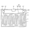
- FIG. 1 is a schematic plan view of a GaN-based field effect transistor according to a first embodiment of the present invention.
- 2 is a cross-sectional view showing a cross section taken along line AA of FIG.
- FIG. 3 is a schematic plan view of a GaN-based field effect transistor according to the second embodiment of the present invention.
- FIG. 4 is a schematic plan view of a GaN-based field effect transistor according to the third embodiment of the present invention.
- FIG. 5 is a schematic plan view of a conventional GaN-based field effect transistor.
- FIG. 6 is a schematic plan view of another conventional GaN-based field effect transistor.
- FIG. 1 is a schematic plan view of a GaN-based HFET (heterojunction field effect transistor) according to the first embodiment of the present invention.
- FIG. 2 is a cross-sectional view showing a cross section taken along line AA of FIG.
- a buffer layer 2, a GaN layer 3, and an AlGaN layer 4 are sequentially formed on a Si substrate 1.
- the GaN layer 3 and the AlGaN layer 4 constitute a GaN-based laminate 5 having a heterojunction. 2DEG (two-dimensional electron gas) is generated at the interface between the GaN layer 3 and the AlGaN layer 4 to form a channel.
- the substrate is not limited to the Si substrate, and a sapphire substrate or SiC substrate may be used.
- the GaN-based laminate 5 may be grown on the sapphire substrate or SiC substrate, or an AlGaN layer is grown on the GaN substrate.
- the GaN-based stacked body 5 may be grown on a substrate made of a nitride semiconductor.
- the buffer layer 2 may not be formed on the Si substrate 1.
- a protective film 7 and an interlayer insulating film 8 are sequentially formed on the GaN-based stacked body 5.
- the material of the protective film 7 for example, SiN is used here, but SiO 2 , Al 2 O 3 or the like may be used.
- the material of the interlayer insulating film 8 for example, a SiO 2 film by CVD is used here, but an insulating material such as SOG (Spin On Glass) or BPSG (Boron Phosphorous Silicate Glass) may be used.
- the thickness of the SiN protective film 7 is 150 nm as an example here, but may be set in a range of 20 nm to 250 nm.
- a recess that penetrates the protective film 7 and the interlayer insulating film 8 and reaches the AlGaN layer 4 is formed, and a drain ohmic electrode 11 and a source ohmic electrode 12 are formed in the recess.
- the drain ohmic electrode 11 and the source ohmic electrode 12 are ohmic electrodes made of ohmic metal, and specifically, are Ti / Al / TiN electrodes in which a Ti layer, an Al layer, and a TiN layer are sequentially laminated.
- the Al film thickness is 10 nm to 300 nm.
- a drain electrode portion 14 is connected to the drain ohmic electrode 11 through a via hole formed in the interlayer insulating film 8.
- a source electrode portion 15 is connected to the source ohmic electrode 12 through a via hole formed in the interlayer insulating film 8.
- the drain electrode portion 14 and the source electrode portion 15 are Ti / AlCu / TiN electrodes in which a Ti layer, an AlCu layer, and a TiN layer are sequentially stacked.
- the AlCu film thickness is 1000 nm to 3000 nm.
- An opening is formed in the protective film 7 between the drain ohmic electrode 11 and the source ohmic electrode 12.
- a gate insulating film 9 and a gate electrode 13 are formed in the opening and in the vicinity thereof.
- the gate electrode 13 is covered with the interlayer insulating film 8.
- a gate electrode pad (not shown) is formed on the interlayer insulating film 8.
- the gate insulating film 9 is a SiN film.
- the gate electrode 13 is made of TiN.
- the drain ohmic electrode 11 and the source ohmic electrode 12 extend in a finger shape in the first direction and in advance in a second direction substantially orthogonal to the first direction. A plurality of them are alternately arranged substantially in parallel with a predetermined interval.
- the interlayer insulating film 8, the drain electrode portion 14, and the source electrode portion 15 are omitted.
- the gate electrode 13 extends in the first direction between the drain ohmic electrode 11 on the finger and the finger-like source electrode 12 in a plan view, and has an annular shape so as to surround the drain ohmic electrode 11. It is extended.
- Both end portions of the gate electrode 13 in the first direction are connected to the gate electrode pad 16 via the gate electrode connection wiring 21, respectively.
- the gate electrode pad 16 is disposed on one end side of the gate electrode 13 in the first direction.
- the gate electrode connection wiring 21 has a first wiring 22 and a second wiring 23.
- the gate electrode connection wiring 21 is a Ti / AlCu / TiN electrode in which a Ti layer, an AlCu layer, and a TiN layer are sequentially stacked.
- the drain ohmic electrode 11, the gate electrode 13 surrounding the drain ohmic electrode 11, a part of the first wiring 22, and a part of the second wiring 23 constitute a gate finger 19.
- the GaN-based HFET has a plurality of gate fingers 19 arranged in the second direction.
- the first wiring 22 is connected to one end portion of each gate electrode 13 in the first direction, and is connected to the gate electrode pad 16, and the one end portion of each gate electrode 13 and the gate electrode pad 16 are electrically connected. Connected.
- One resistance element 17 as an example of an impedance adjustment unit is connected to the first wiring 22.
- the second wiring 23 is connected to the other end of each gate electrode 13 in the first direction, and is connected to the gate electrode pad 16.
- the other end of each gate electrode 13 and the gate electrode pad 16 are connected to each other. Are electrically connected.
- the resistance element 17 is located between one end of each gate electrode 13 and the gate electrode pad 16.
- the resistive element 17 is made of ohmic metal, and specifically, Ti / Al / TiN in which a Ti layer, an Al layer, and a TiN layer, which are the same layers as the drain ohmic electrode 11 and the source ohmic electrode 12, are sequentially laminated. Electrode.
- the resistance element 17 is an adjustment resistor whose resistance value can be adjusted, and the impedance of the first wiring 22 including the resistance element 17 can be adjusted.
- the sheet resistance value of the resistance element 17 is set so that the CR time constant of the first wiring 22 including the resistance element 17 and the CR time constant of the second wiring 23 are substantially the same. Yes.
- the sheet resistance value of the resistance element 17 is, for example, about 10 times the sheet resistance value of the gate electrode connection wiring 21.
- the resistance element 17 can adjust the impedance of the first wiring 22 including the resistance element 17. For this reason, the impedance of the first wiring 22 with respect to the gate signal is adjusted by the resistance element 17 so that the CR time constant of the first wiring 22 and the CR time constant of the second wiring 23 are substantially the same. it can. Thereby, it is possible to prevent a signal delay from occurring in the GaN-based HFET.
- the GaN-based HFET can be operated uniformly with a simple configuration in which the impedance of the first wiring 22 is simply adjusted by the resistance element 17, ringing and surge voltage can be sufficiently suppressed, and stable operation of the GaN-based HFET. Can be realized.
- the drain ohmic electrode 11, the source ohmic electrode 12 and the resistance element 17 are made of the same ohmic metal, the drain electrode 11, the source electrode 12 and the resistance element 17 can be formed in the same process. For this reason, it is not necessary to add another process or perform masking in order to provide the resistance element 17, and the manufacturing cost can be reduced.
- a plurality of drain ohmic electrodes 11 and source ohmic electrodes 12 extending in the finger shape are provided. For this reason, a large current can be passed through the GaN-based HFET, and even when a large current is passed, the operation can be performed uniformly, ringing and surge voltage can be sufficiently suppressed, and stable operation of the GaN-based HFET can be realized.
- FIG. 3 is a schematic plan view of the GaN-based HFET of the second embodiment. The difference from the first embodiment will be described.
- two resistance elements 217 and 217 are connected to the first wiring 222 of the gate electrode connection wiring 221.
- the same reference numerals as those in the first embodiment are the same as those in the first embodiment, and the description thereof is omitted.
- both ends of the first wiring 222 of the gate electrode connection wiring 221 are connected to the gate electrode pad 16 via a part of the second wiring 223 of the gate electrode connection wiring 221, respectively.
- Resistive elements 217 and 217 are connected to both ends 222A and 222B of the first wiring 222, respectively.
- the sheet resistance values of the resistance elements 217 and 217 are set so that the CR time constant of the first wiring 222 and the CR time constant of the second wiring 223 are substantially the same.
- the GaN-based HFET of this embodiment a part of the first wiring 222 and a part of the second wiring 223 overlap. For this reason, the difference between the CR time constant of the first wiring 222 and the CR time constant of the second wiring 223 is smaller than when the first wiring 222 and the second wiring 223 do not overlap. Therefore, it is possible to more reliably prevent the signal delay of the GaN-based HFET. Accordingly, the GaN-based HFET can be operated more uniformly, and ringing and surge voltage can be suppressed.
- FIG. 4 is a schematic plan view of the GaN-based HFET of the third embodiment. The difference from the first embodiment will be described.
- no resistance element is connected to the first wiring 322 of the gate electrode connection wiring 321, and both end portions of the first wiring 322 are connected.
- 322A and 322B constitute an impedance adjustment unit.
- the same reference numerals as those in the first embodiment are the same as those in the first embodiment, and the description thereof is omitted.
- both ends of the first wiring 322 of the gate electrode connection wiring 321 are connected to the second wiring 323 of the gate electrode connection wiring 321, respectively.
- Both end portions 322A and 322B of the first wiring 322 are formed to bend and meander.
- the CR time constant of the first wiring 322 and the CR time constant of the second wiring 323 are set to be substantially the same due to the resistance of the both ends 322A and 322B of the first wiring 322. That is, both end portions 322A and 322B of the first wiring 322 constitute an impedance adjustment unit 317.
- both end portions 322A and 322B of the first wiring 322 constitute the impedance adjustment unit 317, it is not necessary to provide a separate resistance element or the like as the impedance adjustment unit. For this reason, it is not necessary to add another process for providing a resistance element, increase the chip area, or perform masking, so that the manufacturing cost of the GaN-based HFET can be reduced.
- a plurality of finger-shaped drain ohmic electrodes and a plurality of finger-shaped source ohmic electrodes are provided.
- the present invention is not limited to this, and comb-shaped drain ohmic electrodes and comb-shaped electrodes are provided.
- a source ohmic electrode may be provided.
- the resistance elements 17 and 217 are connected to the first wirings 22 and 222.
- the present invention is not limited to this, and the resistance elements are also connected to the second wiring.
- the resistance element may be connected only to the second wiring without connecting the resistance element to the first wiring.
- both end portions 322A and 322B of the first wiring 322 constitute the impedance adjustment unit 317.
- the present invention is not limited to this, and a part of the second wiring constitutes the impedance adjustment unit.
- a part of the first wiring may not constitute the impedance adjustment unit, and only a part of the second wiring may constitute the impedance adjustment unit.
- the resistance elements 17 and 217 are connected to the first wirings 22 and 222.
- the present invention is not limited to this, and the CR time constant of a wiring such as a capacitor is connected to the first wiring. You may connect the passive element which can adjust this.
- the GaN-based HFET has a plurality of gate fingers 19 arranged in the second direction.
- the present invention is not limited to this, and has one gate finger. May be.
- the field effect transistor of the present invention is A GaN-based laminate 5 having a heterojunction; A drain electrode 11 formed on the GaN-based laminate 5 so as to extend in the first direction; It is formed on the GaN-based stacked body 5 so as to extend in the first direction, and is predetermined in a second direction intersecting the first direction with respect to the drain electrode 11.
- Source electrodes 12 formed at intervals; A gate electrode 13 formed between the drain electrode 11 and the source electrode 12 in a plan view; An insulating layer 8 formed on the GaN-based laminate 5 so as to cover the gate electrode 13; A gate electrode pad 16 formed on the insulating layer 8; First wirings 22, 222, 322 for connecting one end of the gate electrode 13 and the gate electrode pad 16; Second wirings 23, 223, 323 connecting the other end of the gate electrode 13 and the gate electrode pad 16, And an impedance adjusting unit 17, 217, 317 capable of adjusting the impedance of at least one of the first wirings 22, 222, 322 and the second wirings 23, 223, 323. .
- the impedance adjusting units 17, 217, and 317 are connected to at least one of the first wirings 22, 222, 322 and the second wirings 23, 223, 323. Impedance can be adjusted. For this reason, the impedance adjustment units 17, 217, and 317 adjust the impedance caused by the resistance and parasitic capacitance of the first wirings 22, 222, and 322 and the second wirings 23, 223, and 323 with respect to the gate signal.
- the impedance of the first wirings 22, 222, and 322 and the impedance of the second wirings 23, 223, and 323 can be made substantially the same to prevent signal delay from occurring in the field effect transistor.
- the field effect transistor can operate uniformly, ringing and surge voltage can be sufficiently suppressed, and stable operation of the field effect transistor can be realized.
- the impedance adjusting units 17 and 217 are resistance elements provided on at least one of the first wirings 22 and 222 and the second wirings 23 and 223.
- the impedance adjusting units 17 and 217 are resistance elements provided on at least one of the first wirings 22 and 222 and the second wirings 23 and 223. For this reason, the impedance can be adjusted with a simple structure so that the impedance of the first wirings 22 and 222 and the impedance of the second wirings 23 and 223 are substantially the same.
- the drain electrode 11, the source electrode 12, and the impedance adjusting portions 17 and 217 are made of ohmic metal.
- the drain electrode 11, the source electrode 12, and the impedance adjustment units 17, 217 are made of ohmic metal, the drain electrode 11, the source electrode 12, and the impedance adjustment units 17, 217 are formed in the same process. it can. For this reason, it is not necessary to add another process or perform masking in order to form the impedance adjusting portions 17 and 217, and the manufacturing cost can be reduced.
- the impedance adjusting unit 317 includes a part of at least one of the first wiring 322 and the second wiring 323.
- a part of at least one of the first wiring 322 and the second wiring 323 constitutes the impedance adjusting unit 317. For this reason, it is not necessary to provide a resistance element separately as an impedance adjustment part. For this reason, it is not necessary to add another process for providing a resistance element, increase the chip area, or perform masking, so that the manufacturing cost of the GaN-based HFET can be reduced.
- the drain electrode 11 and the source electrode 12 are In the second direction, a plurality of them are alternately arranged substantially parallel to each other at intervals, and extend in a finger shape in the first direction.
- the plurality of drain electrodes 11 and source electrodes 12 extending in the finger shape are provided. Therefore, a large current can be passed through the field effect transistor, and even when a large current is passed, the operation can be performed uniformly, ringing and surge voltage can be sufficiently suppressed, and stable operation of the field effect transistor can be realized.
Landscapes
- Junction Field-Effect Transistors (AREA)
- Physics & Mathematics (AREA)
- Geometry (AREA)
Abstract
Description
ヘテロ接合を有するGaN系積層体と、
上記GaN系積層体上に第1の方向に延在するように形成されたドレイン電極と、
上記GaN系積層体上に上記第1の方向に延在するように形成されていると共に、上記ドレイン電極に対して、上記第1の方向と交差する第2の方向に予め定められた間隔をあけて形成されたソース電極と、
平面視において、上記ドレイン電極と上記ソース電極との間に形成されたゲート電極と、
上記GaN系積層体上に、上記ゲート電極を覆うように形成された絶縁層と、
上記絶縁層上に形成されたゲート電極パッドと、
上記ゲート電極の一端部と上記ゲート電極パッドとを接続する第1の配線と、
上記ゲート電極の他端部と上記ゲート電極パッドとを接続する第2の配線と、
上記第1の配線および上記第2の配線のうちの少なくとも1つの配線のインピーダンスを調整可能なインピーダンス調整部と
を備えることを特徴としている。
上記インピーダンス調整部は、上記第1の配線および上記第2の配線のうちの少なくとも1つの配線に設けられた抵抗素子である。
上記ドレイン電極、上記ソース電極および上記インピーダンス調整部がオーミックメタルからなる。
上記インピーダンス調整部は、上記第1の配線および上記第2の配線のうちの少なくとも1つの配線の一部からなる。
上記ドレイン電極と上記ソース電極とは、
上記第2の方向に互いに間隔をあけて略平行に交互に複数配置されていると共に上記第1の方向にフィンガー状に延在している。
図1は、本発明の第1実施形態であるGaN系HFET(ヘテロ接合電界効果トランジスタ)の平面模式図である。また、図2は、図1のA-A線断面を示す断面図である。
図3は、上記第2実施形態のGaN系HFETの平面模式図である。上記第1実施形態と相違する点を説明すると、この第2実施形態では、ゲート電極接続配線221の第1の配線222に2つの抵抗素子217,217が接続されている。なお、この第2実施形態において、上記第1実施形態と同一の符号は、上記第1実施形態と同じ構成であるため、その説明を省略する。
図4は、上記第3実施形態のGaN系HFETの平面模式図である。上記第1実施形態と相違する点を説明すると、この第3実施形態では、ゲート電極接続配線321の第1の配線322には抵抗素子が接続されておらず、第1の配線322の両端部322A,322Bがインピーダンス調整部を構成している。なお、この第3実施形態において、上記第1実施形態と同一の符号は、上記第1実施形態と同じ構成であるため、その説明を省略する。
ヘテロ接合を有するGaN系積層体5と、
上記GaN系積層体5上に第1の方向に延在するように形成されたドレイン電極11と、
上記GaN系積層体5上に上記第1の方向に延在するように形成されていると共に、上記ドレイン電極11に対して、上記第1の方向と交差する第2の方向に予め定められた間隔をあけて形成されたソース電極12と、
平面視において、上記ドレイン電極11と上記ソース電極12との間に形成されたゲート電極13と、
上記GaN系積層体5上に、上記ゲート電極13を覆うように形成された絶縁層8と、
上記絶縁層8上に形成されたゲート電極パッド16と、
上記ゲート電極13の一端部と上記ゲート電極パッド16とを接続する第1の配線22,222,322と、
上記ゲート電極13の他端部と上記ゲート電極パッド16とを接続する第2の配線23,223,323と、
上記第1の配線22,222,322および上記第2の配線23,223,323のうちの少なくとも1つの配線のインピーダンスを調整可能なインピーダンス調整部17,217,317と
を備えることを特徴としている。
上記インピーダンス調整部17,217は、上記第1の配線22,222および上記第2の配線23,223のうちの少なくとも1つの配線に設けられた抵抗素子である。
上記ドレイン電極11、上記ソース電極12および上記インピーダンス調整部17,217がオーミックメタルからなる。
上記インピーダンス調整部317は、上記第1の配線322および上記第2の配線323のうちの少なくとも1つの配線の一部からなる。
上記ドレイン電極11と上記ソース電極12とは、
上記第2の方向に互いに間隔をあけて略平行に交互に複数配置されていると共に上記第1の方向にフィンガー状に延在している。
8 層間絶縁膜
11 ドレインオーミック電極
12 ソースオーミック電極
13 ゲート電極
16 ゲート電極パッド
17,217 抵抗素子
317 インピーダンス調整部
22,222,322 第1の配線
23,223,323 第2の配線
Claims (5)
- ヘテロ接合を有するGaN系積層体(5)と、
上記GaN系積層体(5)上に第1の方向に延在するように形成されたドレイン電極(11)と、
上記GaN系積層体(5)上に上記第1の方向に延在するように形成されていると共に、上記ドレイン電極(11)に対して、上記第1の方向と交差する第2の方向に予め定められた間隔をあけて形成されたソース電極(12)と、
平面視において、上記ドレイン電極(11)と上記ソース電極(12)との間に形成されたゲート電極(13)と、
上記GaN系積層体(5)上に、上記ゲート電極(13)を覆うように形成された絶縁層(8)と、
上記絶縁層(8)上に形成されたゲート電極パッド(16)と、
上記ゲート電極(13)の一端部と上記ゲート電極パッド(16)とを接続する第1の配線(22,222,322)と、
上記ゲート電極(13)の他端部と上記ゲート電極パッド(16)とを接続する第2の配線(23,223,323)と、
上記第1の配線(22,222,322)および上記第2の配線(23,223,323)のうちの少なくとも1つの配線のインピーダンスを調整可能なインピーダンス調整部(17,217,317)と
を備えることを特徴とする電界効果トランジスタ。 - 請求項1に記載の電界効果トランジスタにおいて、
上記インピーダンス調整部(17,217)は、上記第1の配線(22,222)および上記第2の配線(23,223)のうちの少なくとも1つの配線に設けられた抵抗素子であることを特徴とする電界効果トランジスタ。 - 請求項2に記載の電界効果トランジスタにおいて、
上記ドレイン電極(11)、上記ソース電極(12)および上記インピーダンス調整部(17,217)がオーミックメタルからなることを特徴とする電界効果トランジスタ。 - 請求項1に記載の電界効果トランジスタにおいて、
上記インピーダンス調整部(317)は、上記第1の配線(322)および上記第2の配線(323)のうちの少なくとも1つの配線の一部からなることを特徴とする電界効果トランジスタ。 - 請求項1から4のいずれか1つに記載の電界効果トランジスタにおいて、
上記ドレイン電極(11)と上記ソース電極(12)とは、
上記第2の方向に互いに間隔をあけて略平行に交互に複数配置されていると共に上記第1の方向にフィンガー状に延在していることを特徴とする電界効果トランジスタ。
Priority Applications (3)
| Application Number | Priority Date | Filing Date | Title |
|---|---|---|---|
| US15/306,713 US9859411B2 (en) | 2014-05-21 | 2015-02-20 | Field effect transistor |
| CN201580025928.8A CN106463411B (zh) | 2014-05-21 | 2015-02-20 | 场效应晶体管 |
| JP2016520953A JP6106807B2 (ja) | 2014-05-21 | 2015-02-20 | 電界効果トランジスタ |
Applications Claiming Priority (2)
| Application Number | Priority Date | Filing Date | Title |
|---|---|---|---|
| JP2014-105532 | 2014-05-21 | ||
| JP2014105532 | 2014-05-21 |
Publications (1)
| Publication Number | Publication Date |
|---|---|
| WO2015178050A1 true WO2015178050A1 (ja) | 2015-11-26 |
Family
ID=54553728
Family Applications (1)
| Application Number | Title | Priority Date | Filing Date |
|---|---|---|---|
| PCT/JP2015/054866 Ceased WO2015178050A1 (ja) | 2014-05-21 | 2015-02-20 | 電界効果トランジスタ |
Country Status (4)
| Country | Link |
|---|---|
| US (1) | US9859411B2 (ja) |
| JP (1) | JP6106807B2 (ja) |
| CN (1) | CN106463411B (ja) |
| WO (1) | WO2015178050A1 (ja) |
Cited By (1)
| Publication number | Priority date | Publication date | Assignee | Title |
|---|---|---|---|---|
| WO2025258558A1 (ja) * | 2024-06-13 | 2025-12-18 | 国立大学法人東海国立大学機構 | 電界効果トランジスタ |
Families Citing this family (14)
| Publication number | Priority date | Publication date | Assignee | Title |
|---|---|---|---|---|
| JP6617590B2 (ja) * | 2016-02-03 | 2019-12-11 | 富士通株式会社 | 半導体装置 |
| CN110168936B (zh) * | 2016-11-24 | 2023-06-09 | 威电科技有限公司 | 晶体管单元 |
| JP6812764B2 (ja) * | 2016-11-29 | 2021-01-13 | 日亜化学工業株式会社 | 電界効果トランジスタ |
| JP6604495B2 (ja) * | 2017-02-27 | 2019-11-13 | パナソニックIpマネジメント株式会社 | 高周波用トランジスタ |
| WO2018204622A1 (en) * | 2017-05-05 | 2018-11-08 | Cree, Inc. | High power mmic devices having bypassed gate transistors |
| US10218346B1 (en) * | 2017-09-14 | 2019-02-26 | Gan Systems Inc. | High current lateral GaN transistors with scalable topology and gate drive phase equalization |
| US10529802B2 (en) | 2017-09-14 | 2020-01-07 | Gan Systems Inc. | Scalable circuit-under-pad device topologies for lateral GaN power transistors |
| US10811057B1 (en) | 2019-03-26 | 2020-10-20 | Micron Technology, Inc. | Centralized placement of command and address in memory devices |
| US10978117B2 (en) | 2019-03-26 | 2021-04-13 | Micron Technology, Inc. | Centralized placement of command and address swapping in memory devices |
| US10811059B1 (en) | 2019-03-27 | 2020-10-20 | Micron Technology, Inc. | Routing for power signals including a redistribution layer |
| US11031335B2 (en) | 2019-04-03 | 2021-06-08 | Micron Technology, Inc. | Semiconductor devices including redistribution layers |
| DE102020112069B4 (de) | 2020-02-27 | 2022-03-03 | Taiwan Semiconductor Manufacturing Co. Ltd. | Source-leckstromunterdrückung durch source-umgebende gate-struktur und verfahren zur herstellung der gate-struktur |
| US11791388B2 (en) * | 2020-02-27 | 2023-10-17 | Taiwan Semiconductor Manufacturing Company, Ltd. | Source leakage current suppression by source surrounding gate structure |
| US11664431B2 (en) * | 2021-01-08 | 2023-05-30 | Taiwan Semiconductor Manufacturing Company, Ltd. | Ring transistor structure |
Citations (6)
| Publication number | Priority date | Publication date | Assignee | Title |
|---|---|---|---|---|
| JPH04103138A (ja) * | 1990-08-22 | 1992-04-06 | Mitsubishi Electric Corp | 半導体集積回路 |
| JPH05304175A (ja) * | 1991-07-23 | 1993-11-16 | Nec Corp | 電界効果トランジスタおよび高周波信号発振器および周波数変換回路 |
| JPH05304176A (ja) * | 1992-04-27 | 1993-11-16 | Mitsubishi Electric Corp | Fet増幅器 |
| JPH07226488A (ja) * | 1994-02-10 | 1995-08-22 | Nippon Telegr & Teleph Corp <Ntt> | 高周波高出力トランジスタ |
| JPH098063A (ja) * | 1995-06-23 | 1997-01-10 | Nec Corp | 半導体集積装置の製造方法 |
| WO2010113779A1 (ja) * | 2009-03-30 | 2010-10-07 | 日本電気株式会社 | 半導体装置 |
Family Cites Families (6)
| Publication number | Priority date | Publication date | Assignee | Title |
|---|---|---|---|---|
| JPH0687505B2 (ja) | 1987-12-22 | 1994-11-02 | 日本電気株式会社 | 大電力用電界効果トランジスタ |
| US5592006A (en) * | 1994-05-13 | 1997-01-07 | International Rectifier Corporation | Gate resistor for IGBT |
| JP5457046B2 (ja) | 2009-02-13 | 2014-04-02 | パナソニック株式会社 | 半導体装置 |
| JP5457292B2 (ja) * | 2010-07-12 | 2014-04-02 | パナソニック株式会社 | 窒化物半導体装置 |
| JP2012104615A (ja) * | 2010-11-09 | 2012-05-31 | Panasonic Corp | 高周波スイッチおよび高周波モジュール |
| JP2012182438A (ja) * | 2011-02-08 | 2012-09-20 | Toshiba Corp | 半導体装置 |
-
2015
- 2015-02-20 WO PCT/JP2015/054866 patent/WO2015178050A1/ja not_active Ceased
- 2015-02-20 CN CN201580025928.8A patent/CN106463411B/zh active Active
- 2015-02-20 JP JP2016520953A patent/JP6106807B2/ja active Active
- 2015-02-20 US US15/306,713 patent/US9859411B2/en active Active
Patent Citations (6)
| Publication number | Priority date | Publication date | Assignee | Title |
|---|---|---|---|---|
| JPH04103138A (ja) * | 1990-08-22 | 1992-04-06 | Mitsubishi Electric Corp | 半導体集積回路 |
| JPH05304175A (ja) * | 1991-07-23 | 1993-11-16 | Nec Corp | 電界効果トランジスタおよび高周波信号発振器および周波数変換回路 |
| JPH05304176A (ja) * | 1992-04-27 | 1993-11-16 | Mitsubishi Electric Corp | Fet増幅器 |
| JPH07226488A (ja) * | 1994-02-10 | 1995-08-22 | Nippon Telegr & Teleph Corp <Ntt> | 高周波高出力トランジスタ |
| JPH098063A (ja) * | 1995-06-23 | 1997-01-10 | Nec Corp | 半導体集積装置の製造方法 |
| WO2010113779A1 (ja) * | 2009-03-30 | 2010-10-07 | 日本電気株式会社 | 半導体装置 |
Cited By (1)
| Publication number | Priority date | Publication date | Assignee | Title |
|---|---|---|---|---|
| WO2025258558A1 (ja) * | 2024-06-13 | 2025-12-18 | 国立大学法人東海国立大学機構 | 電界効果トランジスタ |
Also Published As
| Publication number | Publication date |
|---|---|
| US20170077276A1 (en) | 2017-03-16 |
| JP6106807B2 (ja) | 2017-04-05 |
| CN106463411B (zh) | 2019-08-20 |
| CN106463411A (zh) | 2017-02-22 |
| US9859411B2 (en) | 2018-01-02 |
| JPWO2015178050A1 (ja) | 2017-04-20 |
Similar Documents
| Publication | Publication Date | Title |
|---|---|---|
| JP6106807B2 (ja) | 電界効果トランジスタ | |
| TWI363424B (ja) | ||
| JP2022191421A (ja) | 半導体装置 | |
| US20170352753A1 (en) | Field-effect transistor | |
| WO2014041731A1 (ja) | 半導体装置 | |
| US9793390B2 (en) | Low miller factor semiconductor device | |
| US9502548B1 (en) | Semiconductor device | |
| TW200830549A (en) | Semiconductor device | |
| US20170301766A1 (en) | Compound semiconductor field effect transistor | |
| WO2016098390A1 (ja) | 電界効果トランジスタ | |
| US9583412B2 (en) | Semiconductor device | |
| JP7161915B2 (ja) | 半導体装置 | |
| JP6584987B2 (ja) | 半導体装置 | |
| WO2014199671A1 (ja) | ヘテロ接合電界効果トランジスタ | |
| WO2012157480A1 (ja) | 電界効果トランジスタ | |
| KR20150107552A (ko) | 반도체 장치 | |
| JP5629736B2 (ja) | 電界効果トランジスタ | |
| WO2012157482A1 (ja) | 電界効果トランジスタ | |
| CN111564494B (zh) | 静电放电保护元件与电路及制造静电放电保护元件的方法 | |
| JP5604490B2 (ja) | 電界効果トランジスタ | |
| KR102034712B1 (ko) | 전력 반도체 소자 및 패키지 | |
| CN112397584B (zh) | 增强型高电子迁移率晶体管元件 | |
| JP6298746B2 (ja) | 電界効果トランジスタ | |
| TWI540703B (zh) | 半導體元件及其製作方法 | |
| CN118591889A (zh) | 半导体装置和半导体模块 |
Legal Events
| Date | Code | Title | Description |
|---|---|---|---|
| 121 | Ep: the epo has been informed by wipo that ep was designated in this application |
Ref document number: 15796294 Country of ref document: EP Kind code of ref document: A1 |
|
| ENP | Entry into the national phase |
Ref document number: 2016520953 Country of ref document: JP Kind code of ref document: A |
|
| WWE | Wipo information: entry into national phase |
Ref document number: 15306713 Country of ref document: US |
|
| NENP | Non-entry into the national phase |
Ref country code: DE |
|
| 122 | Ep: pct application non-entry in european phase |
Ref document number: 15796294 Country of ref document: EP Kind code of ref document: A1 |