WO2015174077A1 - 表示装置および表示装置の駆動方法 - Google Patents
表示装置および表示装置の駆動方法 Download PDFInfo
- Publication number
- WO2015174077A1 WO2015174077A1 PCT/JP2015/002405 JP2015002405W WO2015174077A1 WO 2015174077 A1 WO2015174077 A1 WO 2015174077A1 JP 2015002405 W JP2015002405 W JP 2015002405W WO 2015174077 A1 WO2015174077 A1 WO 2015174077A1
- Authority
- WO
- WIPO (PCT)
- Prior art keywords
- display
- luminance
- deterioration
- amount
- characteristic
- Prior art date
- Legal status (The legal status is an assumption and is not a legal conclusion. Google has not performed a legal analysis and makes no representation as to the accuracy of the status listed.)
- Ceased
Links
Images




Classifications
-
- G—PHYSICS
- G09—EDUCATION; CRYPTOGRAPHY; DISPLAY; ADVERTISING; SEALS
- G09G—ARRANGEMENTS OR CIRCUITS FOR CONTROL OF INDICATING DEVICES USING STATIC MEANS TO PRESENT VARIABLE INFORMATION
- G09G3/00—Control arrangements or circuits, of interest only in connection with visual indicators other than cathode-ray tubes
- G09G3/20—Control arrangements or circuits, of interest only in connection with visual indicators other than cathode-ray tubes for presentation of an assembly of a number of characters, e.g. a page, by composing the assembly by combination of individual elements arranged in a matrix no fixed position being assigned to or needed to be assigned to the individual characters or partial characters
- G09G3/22—Control arrangements or circuits, of interest only in connection with visual indicators other than cathode-ray tubes for presentation of an assembly of a number of characters, e.g. a page, by composing the assembly by combination of individual elements arranged in a matrix no fixed position being assigned to or needed to be assigned to the individual characters or partial characters using controlled light sources
- G09G3/30—Control arrangements or circuits, of interest only in connection with visual indicators other than cathode-ray tubes for presentation of an assembly of a number of characters, e.g. a page, by composing the assembly by combination of individual elements arranged in a matrix no fixed position being assigned to or needed to be assigned to the individual characters or partial characters using controlled light sources using electroluminescent panels
- G09G3/32—Control arrangements or circuits, of interest only in connection with visual indicators other than cathode-ray tubes for presentation of an assembly of a number of characters, e.g. a page, by composing the assembly by combination of individual elements arranged in a matrix no fixed position being assigned to or needed to be assigned to the individual characters or partial characters using controlled light sources using electroluminescent panels semiconductive, e.g. using light-emitting diodes [LED]
- G09G3/3208—Control arrangements or circuits, of interest only in connection with visual indicators other than cathode-ray tubes for presentation of an assembly of a number of characters, e.g. a page, by composing the assembly by combination of individual elements arranged in a matrix no fixed position being assigned to or needed to be assigned to the individual characters or partial characters using controlled light sources using electroluminescent panels semiconductive, e.g. using light-emitting diodes [LED] organic, e.g. using organic light-emitting diodes [OLED]
- G09G3/3225—Control arrangements or circuits, of interest only in connection with visual indicators other than cathode-ray tubes for presentation of an assembly of a number of characters, e.g. a page, by composing the assembly by combination of individual elements arranged in a matrix no fixed position being assigned to or needed to be assigned to the individual characters or partial characters using controlled light sources using electroluminescent panels semiconductive, e.g. using light-emitting diodes [LED] organic, e.g. using organic light-emitting diodes [OLED] using an active matrix
- G09G3/3233—Control arrangements or circuits, of interest only in connection with visual indicators other than cathode-ray tubes for presentation of an assembly of a number of characters, e.g. a page, by composing the assembly by combination of individual elements arranged in a matrix no fixed position being assigned to or needed to be assigned to the individual characters or partial characters using controlled light sources using electroluminescent panels semiconductive, e.g. using light-emitting diodes [LED] organic, e.g. using organic light-emitting diodes [OLED] using an active matrix with pixel circuitry controlling the current through the light-emitting element
-
- G—PHYSICS
- G09—EDUCATION; CRYPTOGRAPHY; DISPLAY; ADVERTISING; SEALS
- G09G—ARRANGEMENTS OR CIRCUITS FOR CONTROL OF INDICATING DEVICES USING STATIC MEANS TO PRESENT VARIABLE INFORMATION
- G09G2310/00—Command of the display device
- G09G2310/08—Details of timing specific for flat panels, other than clock recovery
-
- G—PHYSICS
- G09—EDUCATION; CRYPTOGRAPHY; DISPLAY; ADVERTISING; SEALS
- G09G—ARRANGEMENTS OR CIRCUITS FOR CONTROL OF INDICATING DEVICES USING STATIC MEANS TO PRESENT VARIABLE INFORMATION
- G09G2320/00—Control of display operating conditions
- G09G2320/02—Improving the quality of display appearance
- G09G2320/0233—Improving the luminance or brightness uniformity across the screen
-
- G—PHYSICS
- G09—EDUCATION; CRYPTOGRAPHY; DISPLAY; ADVERTISING; SEALS
- G09G—ARRANGEMENTS OR CIRCUITS FOR CONTROL OF INDICATING DEVICES USING STATIC MEANS TO PRESENT VARIABLE INFORMATION
- G09G2320/00—Control of display operating conditions
- G09G2320/04—Maintaining the quality of display appearance
- G09G2320/043—Preventing or counteracting the effects of ageing
-
- G—PHYSICS
- G09—EDUCATION; CRYPTOGRAPHY; DISPLAY; ADVERTISING; SEALS
- G09G—ARRANGEMENTS OR CIRCUITS FOR CONTROL OF INDICATING DEVICES USING STATIC MEANS TO PRESENT VARIABLE INFORMATION
- G09G2360/00—Aspects of the architecture of display systems
- G09G2360/16—Calculation or use of calculated indices related to luminance levels in display data
Definitions
- the present invention relates to a display device, in particular, a display device using an organic electroluminescence (EL) element and a driving method thereof.
- EL organic electroluminescence
- organic EL element an organic electroluminescence element
- image display apparatus using a current-driven light emitting element.
- organic EL element organic electroluminescence element
- An organic EL display generally includes a plurality of display pixels arranged in a matrix, a plurality of scanning lines and a plurality of data lines connected to the display pixels.
- the display pixel includes an organic EL element, a drive transistor that drives the organic EL element, a selection transistor that switches selection and non-selection of the display pixel, and the like.
- a selection transistor of a display pixel is provided at each of intersections of a plurality of scanning lines and a plurality of data lines, and a storage capacitor element (capacitor) and a gate of a driving transistor are provided in the selection transistor. Is connected.
- the organic EL element deteriorates with time due to a current flowing when displaying an image.
- the deteriorated organic EL element has a lower actual display luminance even when the same amount of current is supplied than before the deterioration.
- the deterioration amount of the organic EL element changes according to the cumulative current amount.
- the luminance signal (luminance data) acquired from the video signal changes with time, and differs for each organic EL element.
- the amount of deterioration varies between organic EL elements.
- video quality may be deteriorated due to variation in the deterioration amount of the organic EL element.
- the present invention provides a display device and a display device driving method capable of reducing deterioration of video quality due to deterioration of light emitting elements with a simpler device configuration.
- a display device includes a display portion including a plurality of display pixels each including a light emitting element, and a reference pixel having a predetermined emission amount attenuation characteristic.
- a control unit that adjusts the luminance signal so that the actual display luminance of the reference pixel when the luminance signal is given is set as the reference display luminance, and the actual display luminance of the display pixel to be corrected becomes the reference display luminance; Is provided.
- the display device and the display device driving method according to the present invention can reduce deterioration in video quality due to deterioration of light emitting elements.
- FIG. 1A is an external view showing an external appearance of an organic EL display.
- FIG. 1B is a block diagram illustrating an example of the configuration of the organic EL display according to the embodiment.
- FIG. 2 is a block diagram illustrating an example of the configuration of the control unit according to the embodiment.
- FIG. 3 is a diagram illustrating an example of the attenuation characteristic, the minimum deterioration characteristic, and the maximum deterioration characteristic of the light emission amount according to the embodiment.
- FIG. 4 is a graph showing the deterioration characteristics before and after correction and the current amount for the first display pixel having the first deterioration characteristic whose deterioration amount is smaller than the attenuation characteristic of the light emission amount.
- FIG. 5 is a graph showing deterioration characteristics and current amounts before and after correction for a second display pixel having a second deterioration characteristic having a larger deterioration amount than the emission amount attenuation characteristic.
- the actual display luminance of the organic EL element decreases with time, that is, deteriorates with time.
- the deterioration amount here is, for example, an integral value.
- the deterioration amount is obtained from, for example, a value obtained by accumulating multiplication values (hereinafter referred to as load amounts) using the light emission time and the current value for all the frames displayed up to now. That is, since the deterioration amount of the organic EL element changes depending on the load amount as well as the current amount, the deterioration amount can be grasped by calculating the load amount from the history of the video signal.
- the amount of current is obtained from the luminance signal (luminance data) of the video signal.
- the deterioration amount is represented, for example, as a ratio of the actual display luminance at the time of calculating the deterioration amount with respect to the initial actual display luminance before deterioration.
- the current amount is used as one of the parameters.
- a display pixel having a larger current amount has a larger load amount and a larger deterioration amount.
- a display pixel with a large amount of current is an area where an image with large luminance data is displayed over a long period of time, such as an area for displaying a logo mark of a broadcast program or an area for displaying time (hereinafter referred to as appropriate).
- This is a display pixel located in a “high luminance region”. Display pixels located in the high brightness area have a larger deterioration amount than display pixels located in the surrounding area (hereinafter referred to as “low brightness area” where appropriate) where an image with relatively small brightness data is displayed. It becomes (burn-in phenomenon).
- the luminance data given to each of the plurality of display pixels constituting one organic EL display is not uniform, and the amount of deterioration of the display pixels varies depending on the luminance data of the video signal. become. If the amount of deterioration varies, as described above, when there are a plurality of display pixels to which the same luminance data is given, the actual display luminance of each display pixel differs depending on the amount of deterioration, and the video quality is degraded. is there.
- the luminance data is reduced for a predetermined period so that the progress of the deterioration is delayed.
- processing for reducing the luminance data is performed for a predetermined period, and the actual display luminance is lowered.
- the actual display brightness of the high brightness area is reduced, and the actual display brightness of the surrounding low brightness area is maintained.
- the difference in the actual display brightness of the image actually displayed on the organic EL display becomes smaller than the brightness difference (brightness data difference) of the video signal included in the broadcast wave, and the video quality deteriorates. There is a problem that there is.
- the relationship of the luminance difference between the luminance data of the video signal and the actual display luminance is maintained while avoiding an unnecessarily long lifetime (the difference between the actual display luminance and the luminance data).
- a display device includes a display portion including a plurality of display pixels each including a light emitting element, and a reference pixel having a predetermined emission amount attenuation characteristic.
- the actual display brightness of the reference pixel when the brightness signal of the display pixel to be corrected is given as the reference display brightness, and the actual display brightness of the display pixel to be corrected becomes the reference display brightness.
- a control unit that adjusts the luminance signal.
- the display device having the above-described configuration performs control so as to align the attenuation characteristics of the light emission amount over time between the plurality of display pixels, instead of aligning the deterioration amounts among the plurality of display pixels. That is, the display device having the above configuration adjusts the luminance signal of the display pixel to be corrected so that the actual display luminance is the same as that of the reference pixel having the attenuation characteristic of the light emission amount. It becomes possible to maintain a luminance difference from the luminance region. Since the display device having the above configuration can maintain the intended luminance difference in the video signal, it can more effectively prevent the video quality from deteriorating.
- the reference pixel is a virtual pixel and does not have to be actually created in the display device.
- the actual display brightness is the amount of light emitted when the display pixels are actually emitted.
- the attenuation characteristic of the light emission amount is defined by the attenuation amount of the actual display luminance with respect to the elapsed time, and the attenuation characteristic of the light emission amount has a larger deterioration amount than the minimum deterioration characteristic that minimizes the deterioration amount with respect to the elapsed time
- the deterioration amount may be set to be smaller than the maximum deterioration characteristic that maximizes the deterioration amount with respect to the elapsed time, and the minimum deterioration characteristic and the maximum deterioration characteristic may be statistically estimated deterioration characteristics.
- the minimum deterioration characteristic and the maximum deterioration characteristic are physical deterioration characteristics obtained statistically.
- the minimum deterioration characteristic and the maximum deterioration characteristic are arbitrary units such as a ratio of the current actual display brightness to the initial actual display brightness, or a difference (size) between the initial actual display brightness and the current actual display brightness. It may be expressed as
- the attenuation characteristic of the light emission amount is set to the minimum deterioration characteristic, the amount of current flowing through the light emitting element is always increased, so that the actual deterioration progress rate of the display pixel is increased and the product life is shortened.
- the attenuation characteristic of the light emission amount is set to the maximum deterioration characteristic, the progress rate of actual deterioration of the display pixel can be delayed, but there is a problem that the attenuation amount of the actual display luminance with time increases.
- the attenuation characteristic of the light emission amount is set so that the deterioration amount is larger than the minimum deterioration characteristic and the deterioration amount is smaller than the maximum deterioration characteristic. For this reason, it is possible to delay the progress rate of the physical deterioration of the display pixel P as compared with the case where the attenuation characteristic of the light emission amount is set to the minimum deterioration characteristic, and the attenuation characteristic of the light emission amount is set to the maximum deterioration characteristic. It is possible to make the attenuation amount of the actual display luminance with time smaller than the case of setting.
- the attenuation characteristic of the light emission amount may be designed in advance according to the specifications of the display device.
- the attenuation characteristic of the light emission amount can be designed according to the specification of the display device, the attenuation amount of the actual display luminance of the display device can be controlled.
- the control unit decreases the luminance signal for a first display pixel having a first deterioration characteristic that is less attenuated with respect to elapsed time than the attenuation characteristic of the light emission amount, and
- the luminance signal may be increased for the second display pixel having the second deterioration characteristic in which the attenuation amount with respect to the elapsed time is larger than the attenuation characteristic of the light emission amount.
- the luminance signal is reduced for the first display pixel having the first deterioration characteristic with the small attenuation amount, and the luminance signal is supplied for the first display pixel having the first deterioration characteristic with the large attenuation amount. increase.
- the light emitting element may be an organic electroluminescence element.
- the organic EL display has a large variation in display pixel deterioration as compared with a liquid crystal display or the like, it is possible to improve or appropriately maintain the video quality by applying the display device having the above configuration.
- a display device driving method is a display device driving method including a display portion including a plurality of display pixels each including a light emitting element, and has a predetermined light emission amount attenuation characteristic.
- the reference display luminance is the actual display luminance when the luminance signal of the display pixel to be corrected is given to the reference pixel having the reference pixel, and the actual display luminance of the display pixel to be corrected becomes the reference display luminance.
- the luminance signal of the display pixel to be corrected is adjusted so that the actual display luminance is the same as that of the reference pixel having the emission amount attenuation characteristic. It becomes possible to maintain a luminance difference from the low luminance region.
- FIGS. 1A to 5 A display device and a driving method thereof according to an embodiment will be described with reference to FIGS. 1A to 5.
- the display device is an organic EL display
- a case where the display device is an organic EL display will be described as an example.
- display devices such as an organic EL display are known to have an actual display luminance that deteriorates with time.
- the display device according to the present embodiment does not completely eliminate the deterioration with time of the actual display brightness, but controls the deterioration with time of the actual display brightness to a characteristic designed in advance. As a result, it is possible to reduce the variation in the degradation of the actual display brightness between products.
- “physical deterioration amount” is the amount of decrease in actual display luminance (emission amount) over time when luminance data obtained from a video signal, that is, uncorrected luminance data is given. I mean. The amount of physical degradation differs between individual display pixels.
- the “attenuation characteristic of the light emission amount” means the attenuation amount of the actual display luminance over time determined by the design.
- the physical deterioration amount cannot be controlled by design (it varies depending on the image to be displayed), but the attenuation characteristic of the light emission amount can be controlled by design.
- the attenuation characteristic of the light emission amount is the same in all display pixels.
- FIG. 1A is an external view showing an external appearance of the organic EL display 1
- FIG. 1B is a block diagram showing a configuration example of the organic EL display 1.
- the organic EL display 1 includes a display unit 10 and a control unit 20.
- the display unit 10 includes an organic EL panel 110, a data line driving circuit 120, and a scanning line driving circuit 130.
- the organic EL panel 110 includes a plurality of display pixels P arranged in a matrix, a plurality of scanning lines GL connected to the display pixels P, and a plurality of data lines SL.
- the display pixel P includes an organic EL element OEL, a selection transistor T1, a driving transistor T2, and a capacitive element C1.
- the selection transistor T1 switches selection / non-selection of the display pixel P in accordance with the drive signal output from the control unit 20.
- the selection transistor T1 is a thin film transistor (TFT: Thin Film Transistor), and has a gate terminal connected to the scanning line GL, a source terminal connected to the data line SL, and a drain terminal connected to the node N1.
- the driving transistor T2 supplies a driving current corresponding to the voltage value of the data line SL to the organic EL element OEL.
- the drive transistor T2 is a thin film transistor, the gate terminal is connected to the node N1, the source terminal is connected to the anode electrode of the organic EL element OEL, and the voltage VTFT is supplied to the drain terminal.
- the organic EL element OEL is a light emitting element that emits light according to a driving current.
- the drive current is supplied from the drive transistor T2.
- the anode electrode is connected to the source terminal of the driving transistor T2, and the cathode electrode is grounded.
- the capacitor element C1 has one end connected to the node N1 and the other end connected to the source terminal of the drive transistor T2.
- the data line driving circuit 120 supplies a voltage corresponding to the correction signal output from the control unit 20 to the data line SL.
- the scanning line driving circuit 130 supplies a voltage corresponding to the driving signal output from the control unit 20 to the scanning line GL.
- the case where the selection transistor T1 and the driving transistor T2 are N-type TFTs has been described as an example.
- a P-type TFT may be used.
- the capacitor C1 is connected between the gate and source of the drive transistor T2.
- the control unit 20 is a circuit that controls display of images on the organic EL panel 110, and is configured using, for example, a TCOM (timing controller). For example, the control unit 20 sequentially acquires the luminance signals of the plurality of display pixels P constituting the organic EL panel 110 from the video signal. Furthermore, the control unit 20 performs correction for each of the luminance signals. The correction of the luminance signal is performed, for example, according to the physical deterioration amount and the light emission amount attenuation characteristic of the organic EL element OEL of the display pixel P corresponding to the luminance signal to be corrected. Hereinafter, the corrected luminance signal is referred to as a correction signal.
- the control unit 20 outputs a correction signal to the data line driving circuit 120.
- the display pixel P corresponding to the correction target luminance signal currently processed in the control unit 20 is referred to as a correction target display pixel P.
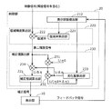
- FIG. 2 is a block diagram illustrating an example of the configuration of the control unit 20.
- the control unit 20 includes a display state detection unit 210, a reduced luminance calculation unit 220, and a correction value calculation unit 230.
- the display state detection unit 210 detects the display state based on the footback signal from the display unit 10.
- the display state here indicates a lighting state of the organic EL panel 110, for example.
- the reduced luminance calculation unit 220 uniformly reduces the luminance signal at the same reduction rate for all the display pixels P of the organic EL panel 110.
- the reduced luminance calculation unit 220 includes a reduction rate calculation unit 221 and a multiplier 222.
- the reduced luminance calculation unit 220 acquires a luminance signal from a video signal for causing the display unit 10 to display an image. Based on the information from the display state detection unit 210, the reduction rate calculation unit 221 obtains a lighting time that is a cumulative time during which an image is displayed on the organic EL panel 110, and derives a reduction rate according to the display time. To do. The reduction rate is set in advance according to the panel lighting time. The multiplier 222 generates the second luminance signal by multiplying the luminance signal acquired from the video signal by the reduction rate calculated by the reduction rate calculation unit 221.
- the correction value calculation unit 230 calculates, for each display pixel P, a correction signal obtained by correcting the second luminance signal according to the deterioration amount.
- the correction value calculation unit 230 includes multipliers 231, 232, and 234, a deterioration amount calculation unit 233, and a correction gradation calculation unit 235. The operation of each component of the correction value calculation unit 230 will be described later.
- the attenuation characteristic of the light emission amount is represented by the decrease amount of the actual display luminance with respect to time as described above.
- the attenuation characteristic of the light emission amount is a characteristic determined by design.
- the attenuation characteristic of the light emission amount may be set according to, for example, the specification of the organic EL display 1, for example, the specification of the product life, for example, the half life of actual display brightness (30,000 hours, 60,000 hours, etc.).
- the attenuation characteristic of the light emission amount in this case is set so that the attenuation amount is larger than the minimum deterioration characteristic L min and smaller than the maximum deterioration characteristic L max at each time.
- the attenuation characteristic of the light emission amount is set in common for all colors so that no color shift occurs between the display pixels P of the same color. It should be noted that the attenuation characteristic of the light emission amount that differs for each color may be set to such an extent that no color misregistration occurs. Further, as described above, the attenuation characteristic of the light emission amount is represented by the amount of decrease in the actual display luminance with respect to time, but it may be attenuated in a linear function or may be attenuated in a quadratic function. . The attenuation characteristic of the light emission amount is stored in advance in a storage unit (not shown) of the organic EL panel 110.
- FIG. 3 is a diagram illustrating an example of the light emission amount attenuation characteristic L0, the minimum deterioration characteristic L min , and the maximum deterioration characteristic L max .
- the attenuation characteristic L0 of the light emission amount is defined by the deterioration rate with respect to the elapsed time.
- the deterioration rate is the ratio of the remaining display luminance of the current display pixel P to the initial actual display luminance of the display pixel P in the initial state (residual display luminance / initial actual display luminance). It is stipulated in.
- the attenuation characteristic L0 of the light emission amount is set so that the deterioration amount is larger than the minimum deterioration characteristic L min and the deterioration amount is smaller than the maximum deterioration characteristic L max at each time.
- the minimum deterioration characteristic L min is represented by, for example, a physical deterioration amount (for example, a deterioration rate) of the display pixel P having the minimum deterioration characteristic with respect to the elapsed time.
- a physical deterioration amount for example, a deterioration rate
- a statistically calculated estimated value or an experimentally calculated value may be used as the physical deterioration amount of the display pixel P having the minimum deterioration characteristic. More specifically, for example, when a test video signal (a normal broadcast wave may be used) is displayed on the organic EL display 1, each of the plurality of display pixels P constituting the organic EL panel 110 is displayed. Determine the amount of degradation.
- the minimum deterioration amount is the physical deterioration amount of the display pixel P having the minimum deterioration characteristic.
- the display pixel P having the minimum deterioration characteristic may be different at each time.
- the maximum deterioration characteristic L max is expressed by, for example, a physical deterioration amount (for example, a deterioration rate) of the display pixel P having the maximum deterioration characteristic with respect to the elapsed time.
- a physical deterioration amount for example, a deterioration rate
- the physical deterioration amount of the display pixel P having the maximum deterioration characteristic for example, an estimated value calculated statistically or a value obtained experimentally may be used. More specifically, for example, when a test video signal (a normal broadcast wave may be used) is displayed on the organic EL display 1, each of the plurality of display pixels P constituting the organic EL panel 110 is displayed. Determine the amount of degradation.
- the maximum deterioration amount is the physical deterioration amount of the display pixel P having the maximum deterioration characteristic.
- the display pixel P having the maximum deterioration characteristic may be different at each time.
- the correction value calculation unit 230 outputs a correction signal to be applied to the correction target display pixel P so that the actual display luminance of the correction target display pixel P is the same as the actual display luminance of the reference pixel to which the second luminance signal is applied. calculate.
- the multiplier 231 multiplies the second luminance signal by (1 / initial efficiency ⁇ 0).
- the actual display brightness that is, the initial actual display brightness L
- I is a current value (corresponding to a luminance signal).
- the multiplier 232 multiplies the output signal (L / ⁇ 0) from the multiplier 231 by (1 / residual rate ⁇ ) calculated by a deterioration amount calculation unit 233 described later.
- the remaining rate ⁇ is a ratio of the current actual display luminance to the initial actual display luminance in the display pixel P to be corrected. Note that the multiplication result L / ( ⁇ 0 ⁇ ⁇ ) of the multiplier 232 is equivalent to the current value that needs to flow through the display pixel P in the organic EL panel 110 in order to obtain the actual display luminance in the initial state.
- the remaining rate is an example of a deterioration amount.
- the ratio of the remaining actual display luminance that is the current actual display luminance of the display pixel P to the initial actual display luminance of the display pixel P (remaining actual display luminance / initial actual display luminance). Brightness).
- the amount of deterioration is obtained from the amount of current actually flowing to the display pixel P, but since it is difficult to directly measure the amount of current, in this embodiment, the amount of deterioration is obtained. Specifically, for example, the multiplication result L / ( ⁇ 0 ⁇ ⁇ ) in the multiplier 232 is obtained.
- Multiplier 234 multiplies the second luminance signal by (1 / residual rate ⁇ ) calculated by deterioration amount calculation unit 233.
- the correction gradation calculation unit 235 specifically sets the luminance signal L / ⁇ adjusted so that the target initial actual display luminance L is generated in the organic EL element OEL having deteriorated, to be specifically set in the display unit 10. To convert to The relationship between gradation and luminance is set in advance, and the gradation corresponding to the luminance signal L / ⁇ is selected by the corrected gradation calculation unit 235.
- FIG. 4 shows the deterioration characteristics before and after correction and the display pixel P for the display pixel P (first display pixel) having the first deterioration characteristic L1 whose deterioration amount (attenuation amount) is smaller than the attenuation characteristic of the light emission amount with respect to the elapsed time. It is a graph which shows the electric current amount I1 which flows.
- the first deterioration characteristic L1 has a smaller deterioration amount with respect to the elapsed time than the light emission attenuation characteristic L0. That is, the amount of deterioration is smaller than the reduction rate defined in the reduced luminance calculation unit 220. For this reason, for the display pixel P having the first deterioration characteristic L1, as a result, processing for reducing the luminance signal input to the control unit 20 is performed. That is, the value of the current amount I1 flowing through the display pixel P having the first deterioration characteristic L1 decreases with time.
- FIG. 5 shows the deterioration characteristics before and after correction and the display pixel P for the display pixel P (second display pixel) having the second deterioration characteristic L2 that has a larger deterioration amount (attenuation amount) with respect to the elapsed time than the emission amount attenuation characteristic. It is a graph which shows the electric current amount I2.
- the second deterioration characteristic L2 has a larger deterioration amount with respect to the elapsed time than the light emission amount attenuation characteristic L0. That is, the amount of deterioration is larger than the reduction rate defined in the reduced luminance calculation unit 220. For this reason, for the display pixel P having the second deterioration characteristic L2, processing for increasing the luminance signal input to the control unit 20 is performed. That is, the value of the current amount I2 flowing through the display pixel P having the second deterioration characteristic L2 increases with time.
- the organic EL display 1 adjusts the luminance signal of the display pixel to be corrected so that the actual display luminance is the same as that of the reference pixel having the emission amount attenuation characteristic. It is possible to maintain the luminance difference between the high luminance region and the low luminance region in the signal. In addition, since the organic EL display 1 of the present embodiment can maintain the intended luminance difference in the video signal, it is possible to effectively avoid the burn-in phenomenon while more effectively preventing the video quality from being deteriorated.
- the organic EL display 1 of the present embodiment does not correct the luminance signal so that the initial actual display luminance can be obtained or the same actual display luminance as that of the pixel having the minimum deterioration characteristic can be obtained.
- the luminance signal is corrected in accordance with the attenuation characteristic of the light emission amount.
- the display pixel with the advanced deterioration (the deterioration amount is large) and the display with the small deterioration amount are displayed. All of the pixels corrected the luminance signal in the direction of increasing the luminance value.
- the luminance signal is corrected in the direction of increasing the luminance value as in the conventional case for the display pixel having a large deterioration amount, but the display pixel having the small deterioration amount is conventionally corrected. On the contrary, the luminance signal is corrected in the direction of decreasing the luminance value.
- the organic EL display 1 of the present embodiment can control the deterioration of the actual display luminance with time by design, it is possible to prevent the video quality from being extremely lowered.
- the organic EL display 1 of the present embodiment can simultaneously exhibit two effects of controlling the deterioration of the actual display luminance with time while suppressing an increase in the physical deterioration amount of the display pixels.
- the video quality can be controlled on the design side.
- the attenuation characteristic of the light emission amount is set according to the product specification of the organic EL display 1, it is possible to control the deterioration of the actual display brightness of the product.
- a non-lighting area and a lighting area are set.
- the data signal from the data line driving circuit 120 shown in FIG. 1B is physically blocked.
- a high load area is applied to the organic EL element (for example, an area where the luminance value is always high) and a low load area where the load is low (for example, an area where the luminance value is always low).
- a non-lighting high load area, a non-lighting low load area, a lighting high load area, and a lighting low load area are set.
- the actual display luminance is adjusted between the lighting high load region and the lighting low load region in order to adjust the actual display luminance according to the attenuation characteristic of the light emission amount.
- the characteristics are considered to match.
- the actual display brightness is measured by physically connecting the non-lighting areas at regular intervals. At this time, the display pixels in the non-lighting region can be considered to maintain an initial state that is not deteriorated because current does not flow except during inspection.
- the luminance signal is corrected so that the non-lighting low load region becomes gradually smaller as described in FIG. That is, the luminance signal is corrected so as to decrease even though the display pixels in the non-lighting low load region are not actually deteriorated. For this reason, it is considered that the actual display luminance of the display pixels in the non-lighting low load region gradually decreases.
- the luminance signal is corrected so as to gradually increase in the non-lighting high load region as described in FIG. That is, the luminance signal is corrected to increase even though the display pixels in the non-lighting high load region are not actually deteriorated. For this reason, it is considered that the actual display luminance of the display pixels in the non-lighting high load region gradually increases.
- the condition a that the attenuation characteristics of the actual display luminance in the lighting high load region and the lighting low load region match, the actual display luminance in the non-lighting low load region gradually decreases, and the actual display luminance in the non-lighting high load region is It is considered that the organic EL display according to the present embodiment is used when the condition b of gradually increasing is satisfied.
- each component may be configured by dedicated hardware or may be realized by executing a software program suitable for each component.
- Each component may be realized by a program execution unit such as a CPU or a processor reading and executing a software program recorded on a recording medium such as a hard disk or a semiconductor memory.
- the software that realizes the display device of the above embodiment is the following program.
- this program sets the actual display brightness when the brightness signal of the display pixel to be corrected is given to the reference pixel having a predetermined emission amount attenuation characteristic to the computer as the reference display brightness.
- the step of adjusting the luminance signal is executed so that the actual display luminance of the display pixel becomes the reference display luminance.
- the display device and the driving method thereof according to the above aspect have been described based on the embodiment, but the present invention is not limited to this embodiment. Without departing from the spirit of the present invention, one or a plurality of aspects are also possible in which various modifications conceived by those skilled in the art have been made in the present embodiment, and forms constructed by combining the constituent elements in the embodiments and modifications. It may be included in the range.
- the display device and display device driving method of the present invention are useful in technical fields such as flat-screen televisions and personal computer displays.
Landscapes
- Engineering & Computer Science (AREA)
- Physics & Mathematics (AREA)
- Computer Hardware Design (AREA)
- General Physics & Mathematics (AREA)
- Theoretical Computer Science (AREA)
- Control Of Indicators Other Than Cathode Ray Tubes (AREA)
- Control Of El Displays (AREA)
- Electroluminescent Light Sources (AREA)
Abstract
Description
上述したように、有機EL素子は、経時的に実表示輝度が低下、つまり、経時劣化する。ここでの劣化量は、例えば、積分値である。具体的には、劣化量は、例えば、現在までに表示された全フレームについて発光時間と電流値を用いた乗算値(以下、負荷量と称する)を累積した値から求められる。即ち、有機EL素子は、電流量と同様に負荷量に応じても劣化量が変化するため、映像信号の履歴から負荷量を算出することで劣化量を把握することができる。電流量は、映像信号の輝度信号(輝度データ)から求められる。
実施の形態の表示装置およびその駆動方法について、図1A~図5を基に説明する。なお、本実施の形態では、表示装置は、有機ELディスプレイである場合を例に説明する。
図1Aは、有機ELディスプレイ1の外観を示す外観図であり、図1Bは、有機ELディスプレイ1の構成例を示すブロック図である。
本実施の形態における表示装置の駆動方法(補正値算出部230の動作)について、図3~図5を基に説明する。
先ず、補正値算出部230の動作の説明に先立って、低減率算出部220で用いる発光量の減衰特性について説明する。
続いて、補正値算出部230の動作(表示装置の駆動方法)の一例について、図2、図4および図5を用いて説明する。なお、以下に示す補正値算出部230の動作は、一例であり、これに限るものではない。
本実施の形態の有機ELディスプレイ1は、上述したように、発光量の減衰特性を有する基準画素と実表示輝度が同じになるように、補正対象の表示画素の輝度信号を調整するため、映像信号における高輝度領域と低輝度領域との輝度差を維持することが可能になる。また、本実施の形態の有機ELディスプレイ1は、映像信号において意図した輝度差を維持できるため、映像品質が低下するのをより効果的に防止しつつ、焼き付き現象を良好に回避できる。
なお、例えば、以下の方法により、本実施の形態の有機ELディスプレイが利用されているか否かを検証することができる。
なお、上記実施の形態において、各構成要素(特に、制御部20)は、専用のハードウェアで構成されるか、各構成要素に適したソフトウェアプログラムを実行することによって実現されてもよい。各構成要素は、CPUまたはプロセッサなどのプログラム実行部が、ハードディスクまたは半導体メモリなどの記録媒体に記録されたソフトウェアプログラムを読み出して実行することによって実現されてもよい。ここで、上記実施の形態の表示装置などを実現するソフトウェアは、次のようなプログラムである。
10 表示部
20 制御部
110 有機ELパネル
120 データ線駆動回路
130 走査線駆動回路
210 表示状態検出部
220 低減輝度算出部
221 低減率算出部
222、231、232、234 乗算器
230 補正値算出部
233 劣化量算出部
235 補正階調算出部
P 表示画素
GL 走査線
SL データ線
OEL 有機EL素子
T1 選択トランジスタ
T2 駆動トランジスタ
C1 容量素子
N1 ノード
L0 発光量の減衰特性
Lmin 最小劣化特性
Lmax 最大劣化特性
Claims (6)
- 発光素子を備える複数の表示画素で構成される表示部と、
予め定められた発光量の減衰特性を有する基準画素に対して、補正対象の表示画素の輝度信号を与えた場合の前記基準画素の実表示輝度を基準表示輝度とし、前記補正対象の表示画素の実表示輝度が前記基準表示輝度となるように、前記輝度信号の調整を行う制御部とを備える
表示装置。 - 前記発光量の減衰特性は、経過時間に対する実表示輝度の減衰量で規定され、
前記発光量の減衰特性は、経過時間に対する減衰量が最小となる最小劣化特性よりも減衰量が大きく、経過時間に対する減衰量が最大となる最大劣化特性よりも減衰量が小さくなるように設定され、
前記最小劣化特性および前記最大劣化特性は、統計的に推定された劣化特性である
請求項1に記載の表示装置。 - 前記発光量の減衰特性は、前記表示装置の仕様に応じて予め設計されている
請求項1または2に記載の表示装置。 - 前記制御部は、前記輝度信号の調整において、
前記発光量の減衰特性よりも経過時間に対する減衰量の小さい第一劣化特性を有する第一表示画素については、前記輝度信号を減少させ、
前記発光量の減衰特性よりも経過時間に対する減衰量の大きい第二劣化特性を有する第二表示画素については、前記輝度信号を増加させる
請求項1~3の何れか1項に記載の表示装置。 - 前記発光素子は、有機エレクトロルミネッセンス素子である
請求項1~4の何れか1項に記載の表示装置。 - 発光素子を備える複数の表示画素で構成される表示部を備える表示装置の駆動方法であって、
予め定められた発光量の減衰特性を有する基準画素に対して、補正対象の表示画素の輝度信号を与えた場合の実表示輝度を基準表示輝度とし、前記補正対象の表示画素の実表示輝度が前記基準表示輝度となるように、前記輝度信号の調整を行うステップを実行する
表示装置の駆動方法。
Priority Applications (2)
| Application Number | Priority Date | Filing Date | Title |
|---|---|---|---|
| US15/310,979 US10304379B2 (en) | 2014-05-15 | 2015-05-12 | Display device and method for driving display device |
| JP2016519115A JPWO2015174077A1 (ja) | 2014-05-15 | 2015-05-12 | 表示装置および表示装置の駆動方法 |
Applications Claiming Priority (2)
| Application Number | Priority Date | Filing Date | Title |
|---|---|---|---|
| JP2014-101764 | 2014-05-15 | ||
| JP2014101764 | 2014-05-15 |
Publications (1)
| Publication Number | Publication Date |
|---|---|
| WO2015174077A1 true WO2015174077A1 (ja) | 2015-11-19 |
Family
ID=54479627
Family Applications (1)
| Application Number | Title | Priority Date | Filing Date |
|---|---|---|---|
| PCT/JP2015/002405 Ceased WO2015174077A1 (ja) | 2014-05-15 | 2015-05-12 | 表示装置および表示装置の駆動方法 |
Country Status (3)
| Country | Link |
|---|---|
| US (1) | US10304379B2 (ja) |
| JP (1) | JPWO2015174077A1 (ja) |
| WO (1) | WO2015174077A1 (ja) |
Cited By (2)
| Publication number | Priority date | Publication date | Assignee | Title |
|---|---|---|---|---|
| WO2022095176A1 (zh) * | 2020-11-09 | 2022-05-12 | 深圳市华星光电半导体显示技术有限公司 | 显示面板亮度调节方法及装置 |
| WO2025032744A1 (ja) * | 2023-08-08 | 2025-02-13 | シャープディスプレイテクノロジー株式会社 | 自発光表示パネルの累積劣化量推定方法、自発光表示装置、表示補正方法、機械学習モデル及び機械学習モデルの構築方法 |
Families Citing this family (5)
| Publication number | Priority date | Publication date | Assignee | Title |
|---|---|---|---|---|
| CN105206217B (zh) * | 2015-10-27 | 2018-02-06 | 京东方科技集团股份有限公司 | 显示处理方法、装置及显示器件 |
| WO2018083928A1 (ja) * | 2016-11-07 | 2018-05-11 | シャープ株式会社 | 画像表示装置および画像表示方法 |
| KR102708366B1 (ko) * | 2019-07-30 | 2024-09-20 | 엘지전자 주식회사 | 디스플레이 장치 및 방법 |
| KR102939960B1 (ko) * | 2020-12-24 | 2026-03-16 | 엘지디스플레이 주식회사 | 열화가 방지된 표시장치 및 이의 열화보상방법 |
| JP2023159520A (ja) * | 2022-04-20 | 2023-11-01 | 武漢天馬微電子有限公司 | 表示装置及び表示装置の制御方法 |
Citations (4)
| Publication number | Priority date | Publication date | Assignee | Title |
|---|---|---|---|---|
| JP2001350442A (ja) * | 1999-10-04 | 2001-12-21 | Matsushita Electric Ind Co Ltd | 表示パネルの駆動方法、表示パネルの輝度補正装置及び駆動装置 |
| JP2006301220A (ja) * | 2005-04-20 | 2006-11-02 | Hitachi Displays Ltd | 表示装置及びその駆動方法 |
| JP2007187761A (ja) * | 2006-01-11 | 2007-07-26 | Sony Corp | 自発光表示装置、見積もり劣化情報修正装置、入力表示データ補正装置及びプログラム |
| WO2013115356A1 (ja) * | 2012-02-02 | 2013-08-08 | 株式会社ニコン | 画像表示装置、電子機器、電子カメラ、及び情報端末 |
Family Cites Families (9)
| Publication number | Priority date | Publication date | Assignee | Title |
|---|---|---|---|---|
| JP3230498B2 (ja) | 1998-10-23 | 2001-11-19 | 日本電気株式会社 | プラズマディスプレイパネル輝度補正装置および方法 |
| JP2000356981A (ja) | 1999-06-16 | 2000-12-26 | Mitsubishi Electric Corp | ディスプレイ表示制御装置 |
| CN1377495A (zh) * | 1999-10-04 | 2002-10-30 | 松下电器产业株式会社 | 显示面板的驱动方法、显示面板的亮度校正装置及其驱动装置 |
| JP2001175221A (ja) | 1999-12-17 | 2001-06-29 | Toshiba Corp | 表示装置 |
| JP2006195310A (ja) | 2005-01-17 | 2006-07-27 | Sony Corp | 焼き付き現象補正方法、自発光装置、焼き付き現象補正装置及びプログラム |
| US8405585B2 (en) * | 2008-01-04 | 2013-03-26 | Chimei Innolux Corporation | OLED display, information device, and method for displaying an image in OLED display |
| JP5293367B2 (ja) * | 2009-04-17 | 2013-09-18 | セイコーエプソン株式会社 | 自発光表示装置および電子機器 |
| US9311859B2 (en) * | 2009-11-30 | 2016-04-12 | Ignis Innovation Inc. | Resetting cycle for aging compensation in AMOLED displays |
| WO2015056446A1 (ja) | 2013-10-18 | 2015-04-23 | パナソニック株式会社 | 表示装置およびその駆動方法 |
-
2015
- 2015-05-12 JP JP2016519115A patent/JPWO2015174077A1/ja active Pending
- 2015-05-12 WO PCT/JP2015/002405 patent/WO2015174077A1/ja not_active Ceased
- 2015-05-12 US US15/310,979 patent/US10304379B2/en active Active
Patent Citations (4)
| Publication number | Priority date | Publication date | Assignee | Title |
|---|---|---|---|---|
| JP2001350442A (ja) * | 1999-10-04 | 2001-12-21 | Matsushita Electric Ind Co Ltd | 表示パネルの駆動方法、表示パネルの輝度補正装置及び駆動装置 |
| JP2006301220A (ja) * | 2005-04-20 | 2006-11-02 | Hitachi Displays Ltd | 表示装置及びその駆動方法 |
| JP2007187761A (ja) * | 2006-01-11 | 2007-07-26 | Sony Corp | 自発光表示装置、見積もり劣化情報修正装置、入力表示データ補正装置及びプログラム |
| WO2013115356A1 (ja) * | 2012-02-02 | 2013-08-08 | 株式会社ニコン | 画像表示装置、電子機器、電子カメラ、及び情報端末 |
Cited By (2)
| Publication number | Priority date | Publication date | Assignee | Title |
|---|---|---|---|---|
| WO2022095176A1 (zh) * | 2020-11-09 | 2022-05-12 | 深圳市华星光电半导体显示技术有限公司 | 显示面板亮度调节方法及装置 |
| WO2025032744A1 (ja) * | 2023-08-08 | 2025-02-13 | シャープディスプレイテクノロジー株式会社 | 自発光表示パネルの累積劣化量推定方法、自発光表示装置、表示補正方法、機械学習モデル及び機械学習モデルの構築方法 |
Also Published As
| Publication number | Publication date |
|---|---|
| JPWO2015174077A1 (ja) | 2017-04-20 |
| US10304379B2 (en) | 2019-05-28 |
| US20170076668A1 (en) | 2017-03-16 |
Similar Documents
| Publication | Publication Date | Title |
|---|---|---|
| WO2015174077A1 (ja) | 表示装置および表示装置の駆動方法 | |
| US8427513B2 (en) | Display device, display device drive method, and computer program | |
| JP6388032B2 (ja) | 表示装置および表示装置の駆動方法 | |
| CN108780626B (zh) | 有机发光二极管显示装置及其操作方法 | |
| KR102279374B1 (ko) | 열화보상장치 및 방법, 이를 포함하는 표시장치 | |
| CN102741910A (zh) | 用于提取有机发光器件的相关曲线的系统和方法 | |
| CN103165076A (zh) | 有机发光显示器及其劣化补偿方法 | |
| JP5218827B2 (ja) | 表示制御装置および方法、並びにプログラム | |
| US9189986B2 (en) | Display panel driving method, display device driving circuit, and display device | |
| JP5779656B2 (ja) | 画像表示装置 | |
| CN103943093A (zh) | 改善无源有机发光二极管显示屏亮度均匀性的方法及装置 | |
| US10762835B2 (en) | Display device and driving method thereof | |
| CN106486056A (zh) | 有机发光二极管显示设备及其驱动方法 | |
| CN110738962A (zh) | 用于显示器oled退化的补偿系统和方法 | |
| JP2015197473A (ja) | 信号処理方法、表示装置、及び電子機器 | |
| US20110115773A1 (en) | Image display and image display method | |
| CN105097872B (zh) | 提取有机发光器件的关联曲线的系统和方法 | |
| CN105210138B (zh) | 集成的补偿数据通道 | |
| JP2008145880A (ja) | 映像補正装置、映像補正方法、プログラム、および映像表示装置 | |
| KR20190034855A (ko) | 유기발광표시장치 및 이의 구동방법 | |
| JPWO2016035294A1 (ja) | 表示装置の補正方法および表示装置の補正装置 | |
| CN105637575A (zh) | 用于amoled像素驱动器的功率节约的系统和方法 | |
| JP5957675B2 (ja) | 自発光表示装置、自発光表示装置の制御方法及びコンピュータプログラム | |
| JP2015004843A (ja) | 表示装置、表示装置の制御方法、及び、プログラム | |
| KR20140129518A (ko) | 유기발광 표시장치와 그 구동 특성 보상 방법 |
Legal Events
| Date | Code | Title | Description |
|---|---|---|---|
| 121 | Ep: the epo has been informed by wipo that ep was designated in this application |
Ref document number: 15793135 Country of ref document: EP Kind code of ref document: A1 |
|
| ENP | Entry into the national phase |
Ref document number: 2016519115 Country of ref document: JP Kind code of ref document: A |
|
| WWE | Wipo information: entry into national phase |
Ref document number: 15310979 Country of ref document: US |
|
| NENP | Non-entry into the national phase |
Ref country code: DE |
|
| 122 | Ep: pct application non-entry in european phase |
Ref document number: 15793135 Country of ref document: EP Kind code of ref document: A1 |