WO2015170738A1 - ワイヤボンディング構造の製造方法、ワイヤボンディング構造、電子装置 - Google Patents
ワイヤボンディング構造の製造方法、ワイヤボンディング構造、電子装置 Download PDFInfo
- Publication number
- WO2015170738A1 WO2015170738A1 PCT/JP2015/063293 JP2015063293W WO2015170738A1 WO 2015170738 A1 WO2015170738 A1 WO 2015170738A1 JP 2015063293 W JP2015063293 W JP 2015063293W WO 2015170738 A1 WO2015170738 A1 WO 2015170738A1
- Authority
- WO
- WIPO (PCT)
- Prior art keywords
- wire
- electronic device
- bonding
- bonding pad
- target
- Prior art date
- Legal status (The legal status is an assumption and is not a legal conclusion. Google has not performed a legal analysis and makes no representation as to the accuracy of the status listed.)
- Ceased
Links
Images


























Classifications
-
- B—PERFORMING OPERATIONS; TRANSPORTING
- B23—MACHINE TOOLS; METAL-WORKING NOT OTHERWISE PROVIDED FOR
- B23K—SOLDERING OR UNSOLDERING; WELDING; CLADDING OR PLATING BY SOLDERING OR WELDING; CUTTING BY APPLYING HEAT LOCALLY, e.g. FLAME CUTTING; WORKING BY LASER BEAM
- B23K20/00—Non-electric welding by applying impact or other pressure, with or without the application of heat, e.g. cladding or plating
- B23K20/12—Non-electric welding by applying impact or other pressure, with or without the application of heat, e.g. cladding or plating the heat being generated by friction; Friction welding
- B23K20/129—Non-electric welding by applying impact or other pressure, with or without the application of heat, e.g. cladding or plating the heat being generated by friction; Friction welding specially adapted for particular articles or work
-
- B—PERFORMING OPERATIONS; TRANSPORTING
- B23—MACHINE TOOLS; METAL-WORKING NOT OTHERWISE PROVIDED FOR
- B23K—SOLDERING OR UNSOLDERING; WELDING; CLADDING OR PLATING BY SOLDERING OR WELDING; CUTTING BY APPLYING HEAT LOCALLY, e.g. FLAME CUTTING; WORKING BY LASER BEAM
- B23K20/00—Non-electric welding by applying impact or other pressure, with or without the application of heat, e.g. cladding or plating
- B23K20/10—Non-electric welding by applying impact or other pressure, with or without the application of heat, e.g. cladding or plating making use of vibrations, e.g. ultrasonic welding
-
- B—PERFORMING OPERATIONS; TRANSPORTING
- B23—MACHINE TOOLS; METAL-WORKING NOT OTHERWISE PROVIDED FOR
- B23K—SOLDERING OR UNSOLDERING; WELDING; CLADDING OR PLATING BY SOLDERING OR WELDING; CUTTING BY APPLYING HEAT LOCALLY, e.g. FLAME CUTTING; WORKING BY LASER BEAM
- B23K20/00—Non-electric welding by applying impact or other pressure, with or without the application of heat, e.g. cladding or plating
- B23K20/12—Non-electric welding by applying impact or other pressure, with or without the application of heat, e.g. cladding or plating the heat being generated by friction; Friction welding
- B23K20/1205—Non-electric welding by applying impact or other pressure, with or without the application of heat, e.g. cladding or plating the heat being generated by friction; Friction welding using translation movement
-
- H—ELECTRICITY
- H10—SEMICONDUCTOR DEVICES; ELECTRIC SOLID-STATE DEVICES NOT OTHERWISE PROVIDED FOR
- H10W—GENERIC PACKAGES, INTERCONNECTIONS, CONNECTORS OR OTHER CONSTRUCTIONAL DETAILS OF DEVICES COVERED BY CLASS H10
- H10W40/00—Arrangements for thermal protection or thermal control
- H10W40/01—Manufacture or treatment
- H10W40/03—Manufacture or treatment of arrangements for cooling
- H10W40/037—Assembling together parts thereof
-
- H—ELECTRICITY
- H10—SEMICONDUCTOR DEVICES; ELECTRIC SOLID-STATE DEVICES NOT OTHERWISE PROVIDED FOR
- H10W—GENERIC PACKAGES, INTERCONNECTIONS, CONNECTORS OR OTHER CONSTRUCTIONAL DETAILS OF DEVICES COVERED BY CLASS H10
- H10W70/00—Package substrates; Interposers; Redistribution layers [RDL]
- H10W70/01—Manufacture or treatment
- H10W70/04—Manufacture or treatment of leadframes
- H10W70/041—Connecting or disconnecting interconnections to or from leadframes, e.g. connecting bond wires or bumps
-
- H—ELECTRICITY
- H10—SEMICONDUCTOR DEVICES; ELECTRIC SOLID-STATE DEVICES NOT OTHERWISE PROVIDED FOR
- H10W—GENERIC PACKAGES, INTERCONNECTIONS, CONNECTORS OR OTHER CONSTRUCTIONAL DETAILS OF DEVICES COVERED BY CLASS H10
- H10W70/00—Package substrates; Interposers; Redistribution layers [RDL]
- H10W70/40—Leadframes
- H10W70/411—Chip-supporting parts, e.g. die pads
- H10W70/417—Bonding materials between chips and die pads
-
- H—ELECTRICITY
- H10—SEMICONDUCTOR DEVICES; ELECTRIC SOLID-STATE DEVICES NOT OTHERWISE PROVIDED FOR
- H10W—GENERIC PACKAGES, INTERCONNECTIONS, CONNECTORS OR OTHER CONSTRUCTIONAL DETAILS OF DEVICES COVERED BY CLASS H10
- H10W70/00—Package substrates; Interposers; Redistribution layers [RDL]
- H10W70/40—Leadframes
- H10W70/456—Materials
- H10W70/457—Materials of metallic layers on leadframes
-
- H—ELECTRICITY
- H10—SEMICONDUCTOR DEVICES; ELECTRIC SOLID-STATE DEVICES NOT OTHERWISE PROVIDED FOR
- H10W—GENERIC PACKAGES, INTERCONNECTIONS, CONNECTORS OR OTHER CONSTRUCTIONAL DETAILS OF DEVICES COVERED BY CLASS H10
- H10W70/00—Package substrates; Interposers; Redistribution layers [RDL]
- H10W70/40—Leadframes
- H10W70/461—Leadframes specially adapted for cooling
-
- H—ELECTRICITY
- H10—SEMICONDUCTOR DEVICES; ELECTRIC SOLID-STATE DEVICES NOT OTHERWISE PROVIDED FOR
- H10W—GENERIC PACKAGES, INTERCONNECTIONS, CONNECTORS OR OTHER CONSTRUCTIONAL DETAILS OF DEVICES COVERED BY CLASS H10
- H10W70/00—Package substrates; Interposers; Redistribution layers [RDL]
- H10W70/40—Leadframes
- H10W70/464—Additional interconnections in combination with leadframes
- H10W70/465—Bumps or wires
-
- H—ELECTRICITY
- H10—SEMICONDUCTOR DEVICES; ELECTRIC SOLID-STATE DEVICES NOT OTHERWISE PROVIDED FOR
- H10W—GENERIC PACKAGES, INTERCONNECTIONS, CONNECTORS OR OTHER CONSTRUCTIONAL DETAILS OF DEVICES COVERED BY CLASS H10
- H10W70/00—Package substrates; Interposers; Redistribution layers [RDL]
- H10W70/40—Leadframes
- H10W70/481—Leadframes for devices being provided for in groups H10D8/00 - H10D48/00
-
- H—ELECTRICITY
- H10—SEMICONDUCTOR DEVICES; ELECTRIC SOLID-STATE DEVICES NOT OTHERWISE PROVIDED FOR
- H10W—GENERIC PACKAGES, INTERCONNECTIONS, CONNECTORS OR OTHER CONSTRUCTIONAL DETAILS OF DEVICES COVERED BY CLASS H10
- H10W72/00—Interconnections or connectors in packages
- H10W72/071—Connecting or disconnecting
- H10W72/072—Connecting or disconnecting of bump connectors
-
- H—ELECTRICITY
- H10—SEMICONDUCTOR DEVICES; ELECTRIC SOLID-STATE DEVICES NOT OTHERWISE PROVIDED FOR
- H10W—GENERIC PACKAGES, INTERCONNECTIONS, CONNECTORS OR OTHER CONSTRUCTIONAL DETAILS OF DEVICES COVERED BY CLASS H10
- H10W72/00—Interconnections or connectors in packages
- H10W72/20—Bump connectors, e.g. solder bumps or copper pillars; Dummy bumps; Thermal bumps
-
- H—ELECTRICITY
- H10—SEMICONDUCTOR DEVICES; ELECTRIC SOLID-STATE DEVICES NOT OTHERWISE PROVIDED FOR
- H10W—GENERIC PACKAGES, INTERCONNECTIONS, CONNECTORS OR OTHER CONSTRUCTIONAL DETAILS OF DEVICES COVERED BY CLASS H10
- H10W74/00—Encapsulations, e.g. protective coatings
- H10W74/01—Manufacture or treatment
- H10W74/016—Manufacture or treatment using moulds
-
- H—ELECTRICITY
- H10—SEMICONDUCTOR DEVICES; ELECTRIC SOLID-STATE DEVICES NOT OTHERWISE PROVIDED FOR
- H10W—GENERIC PACKAGES, INTERCONNECTIONS, CONNECTORS OR OTHER CONSTRUCTIONAL DETAILS OF DEVICES COVERED BY CLASS H10
- H10W74/00—Encapsulations, e.g. protective coatings
- H10W74/10—Encapsulations, e.g. protective coatings characterised by their shape or disposition
- H10W74/111—Encapsulations, e.g. protective coatings characterised by their shape or disposition the semiconductor body being completely enclosed
- H10W74/129—Encapsulations, e.g. protective coatings characterised by their shape or disposition the semiconductor body being completely enclosed forming a chip-scale package [CSP]
-
- H—ELECTRICITY
- H10—SEMICONDUCTOR DEVICES; ELECTRIC SOLID-STATE DEVICES NOT OTHERWISE PROVIDED FOR
- H10W—GENERIC PACKAGES, INTERCONNECTIONS, CONNECTORS OR OTHER CONSTRUCTIONAL DETAILS OF DEVICES COVERED BY CLASS H10
- H10W72/00—Interconnections or connectors in packages
- H10W72/01—Manufacture or treatment
- H10W72/015—Manufacture or treatment of bond wires
- H10W72/01551—Changing the shapes of bond wires
-
- H—ELECTRICITY
- H10—SEMICONDUCTOR DEVICES; ELECTRIC SOLID-STATE DEVICES NOT OTHERWISE PROVIDED FOR
- H10W—GENERIC PACKAGES, INTERCONNECTIONS, CONNECTORS OR OTHER CONSTRUCTIONAL DETAILS OF DEVICES COVERED BY CLASS H10
- H10W72/00—Interconnections or connectors in packages
- H10W72/071—Connecting or disconnecting
- H10W72/0711—Apparatus therefor
- H10W72/07141—Means for applying energy, e.g. ovens or lasers
-
- H—ELECTRICITY
- H10—SEMICONDUCTOR DEVICES; ELECTRIC SOLID-STATE DEVICES NOT OTHERWISE PROVIDED FOR
- H10W—GENERIC PACKAGES, INTERCONNECTIONS, CONNECTORS OR OTHER CONSTRUCTIONAL DETAILS OF DEVICES COVERED BY CLASS H10
- H10W72/00—Interconnections or connectors in packages
- H10W72/071—Connecting or disconnecting
- H10W72/0711—Apparatus therefor
- H10W72/07163—Means for mechanical processing, e.g. for planarising, pressing, stamping or drilling
-
- H—ELECTRICITY
- H10—SEMICONDUCTOR DEVICES; ELECTRIC SOLID-STATE DEVICES NOT OTHERWISE PROVIDED FOR
- H10W—GENERIC PACKAGES, INTERCONNECTIONS, CONNECTORS OR OTHER CONSTRUCTIONAL DETAILS OF DEVICES COVERED BY CLASS H10
- H10W72/00—Interconnections or connectors in packages
- H10W72/071—Connecting or disconnecting
- H10W72/0711—Apparatus therefor
- H10W72/07178—Means for aligning
-
- H—ELECTRICITY
- H10—SEMICONDUCTOR DEVICES; ELECTRIC SOLID-STATE DEVICES NOT OTHERWISE PROVIDED FOR
- H10W—GENERIC PACKAGES, INTERCONNECTIONS, CONNECTORS OR OTHER CONSTRUCTIONAL DETAILS OF DEVICES COVERED BY CLASS H10
- H10W72/00—Interconnections or connectors in packages
- H10W72/071—Connecting or disconnecting
- H10W72/073—Connecting or disconnecting of die-attach connectors
-
- H—ELECTRICITY
- H10—SEMICONDUCTOR DEVICES; ELECTRIC SOLID-STATE DEVICES NOT OTHERWISE PROVIDED FOR
- H10W—GENERIC PACKAGES, INTERCONNECTIONS, CONNECTORS OR OTHER CONSTRUCTIONAL DETAILS OF DEVICES COVERED BY CLASS H10
- H10W72/00—Interconnections or connectors in packages
- H10W72/071—Connecting or disconnecting
- H10W72/073—Connecting or disconnecting of die-attach connectors
- H10W72/07331—Connecting techniques
- H10W72/07336—Soldering or alloying
-
- H—ELECTRICITY
- H10—SEMICONDUCTOR DEVICES; ELECTRIC SOLID-STATE DEVICES NOT OTHERWISE PROVIDED FOR
- H10W—GENERIC PACKAGES, INTERCONNECTIONS, CONNECTORS OR OTHER CONSTRUCTIONAL DETAILS OF DEVICES COVERED BY CLASS H10
- H10W72/00—Interconnections or connectors in packages
- H10W72/071—Connecting or disconnecting
- H10W72/075—Connecting or disconnecting of bond wires
-
- H—ELECTRICITY
- H10—SEMICONDUCTOR DEVICES; ELECTRIC SOLID-STATE DEVICES NOT OTHERWISE PROVIDED FOR
- H10W—GENERIC PACKAGES, INTERCONNECTIONS, CONNECTORS OR OTHER CONSTRUCTIONAL DETAILS OF DEVICES COVERED BY CLASS H10
- H10W72/00—Interconnections or connectors in packages
- H10W72/071—Connecting or disconnecting
- H10W72/075—Connecting or disconnecting of bond wires
- H10W72/07511—Treating the bonding area before connecting, e.g. by applying flux or cleaning
-
- H—ELECTRICITY
- H10—SEMICONDUCTOR DEVICES; ELECTRIC SOLID-STATE DEVICES NOT OTHERWISE PROVIDED FOR
- H10W—GENERIC PACKAGES, INTERCONNECTIONS, CONNECTORS OR OTHER CONSTRUCTIONAL DETAILS OF DEVICES COVERED BY CLASS H10
- H10W72/00—Interconnections or connectors in packages
- H10W72/071—Connecting or disconnecting
- H10W72/075—Connecting or disconnecting of bond wires
- H10W72/07521—Aligning
-
- H—ELECTRICITY
- H10—SEMICONDUCTOR DEVICES; ELECTRIC SOLID-STATE DEVICES NOT OTHERWISE PROVIDED FOR
- H10W—GENERIC PACKAGES, INTERCONNECTIONS, CONNECTORS OR OTHER CONSTRUCTIONAL DETAILS OF DEVICES COVERED BY CLASS H10
- H10W72/00—Interconnections or connectors in packages
- H10W72/071—Connecting or disconnecting
- H10W72/075—Connecting or disconnecting of bond wires
- H10W72/07521—Aligning
- H10W72/07527—Aligning involving guiding structures, e.g. spacers or supporting members
-
- H—ELECTRICITY
- H10—SEMICONDUCTOR DEVICES; ELECTRIC SOLID-STATE DEVICES NOT OTHERWISE PROVIDED FOR
- H10W—GENERIC PACKAGES, INTERCONNECTIONS, CONNECTORS OR OTHER CONSTRUCTIONAL DETAILS OF DEVICES COVERED BY CLASS H10
- H10W72/00—Interconnections or connectors in packages
- H10W72/071—Connecting or disconnecting
- H10W72/075—Connecting or disconnecting of bond wires
- H10W72/07531—Techniques
- H10W72/07532—Compression bonding, e.g. thermocompression bonding
- H10W72/07533—Ultrasonic bonding, e.g. thermosonic bonding
-
- H—ELECTRICITY
- H10—SEMICONDUCTOR DEVICES; ELECTRIC SOLID-STATE DEVICES NOT OTHERWISE PROVIDED FOR
- H10W—GENERIC PACKAGES, INTERCONNECTIONS, CONNECTORS OR OTHER CONSTRUCTIONAL DETAILS OF DEVICES COVERED BY CLASS H10
- H10W72/00—Interconnections or connectors in packages
- H10W72/071—Connecting or disconnecting
- H10W72/075—Connecting or disconnecting of bond wires
- H10W72/07551—Connecting or disconnecting of bond wires characterised by changes in properties of the bond wires during the connecting
- H10W72/07552—Connecting or disconnecting of bond wires characterised by changes in properties of the bond wires during the connecting changes in structures or sizes
-
- H—ELECTRICITY
- H10—SEMICONDUCTOR DEVICES; ELECTRIC SOLID-STATE DEVICES NOT OTHERWISE PROVIDED FOR
- H10W—GENERIC PACKAGES, INTERCONNECTIONS, CONNECTORS OR OTHER CONSTRUCTIONAL DETAILS OF DEVICES COVERED BY CLASS H10
- H10W72/00—Interconnections or connectors in packages
- H10W72/30—Die-attach connectors
- H10W72/321—Structures or relative sizes of die-attach connectors
- H10W72/325—Die-attach connectors having a filler embedded in a matrix
-
- H—ELECTRICITY
- H10—SEMICONDUCTOR DEVICES; ELECTRIC SOLID-STATE DEVICES NOT OTHERWISE PROVIDED FOR
- H10W—GENERIC PACKAGES, INTERCONNECTIONS, CONNECTORS OR OTHER CONSTRUCTIONAL DETAILS OF DEVICES COVERED BY CLASS H10
- H10W72/00—Interconnections or connectors in packages
- H10W72/30—Die-attach connectors
- H10W72/351—Materials of die-attach connectors
- H10W72/352—Materials of die-attach connectors comprising metals or metalloids, e.g. solders
-
- H—ELECTRICITY
- H10—SEMICONDUCTOR DEVICES; ELECTRIC SOLID-STATE DEVICES NOT OTHERWISE PROVIDED FOR
- H10W—GENERIC PACKAGES, INTERCONNECTIONS, CONNECTORS OR OTHER CONSTRUCTIONAL DETAILS OF DEVICES COVERED BY CLASS H10
- H10W72/00—Interconnections or connectors in packages
- H10W72/50—Bond wires
- H10W72/521—Structures or relative sizes of bond wires
- H10W72/527—Multiple bond wires having different sizes
-
- H—ELECTRICITY
- H10—SEMICONDUCTOR DEVICES; ELECTRIC SOLID-STATE DEVICES NOT OTHERWISE PROVIDED FOR
- H10W—GENERIC PACKAGES, INTERCONNECTIONS, CONNECTORS OR OTHER CONSTRUCTIONAL DETAILS OF DEVICES COVERED BY CLASS H10
- H10W72/00—Interconnections or connectors in packages
- H10W72/50—Bond wires
- H10W72/531—Shapes of wire connectors
- H10W72/5363—Shapes of wire connectors the connected ends being wedge-shaped
-
- H—ELECTRICITY
- H10—SEMICONDUCTOR DEVICES; ELECTRIC SOLID-STATE DEVICES NOT OTHERWISE PROVIDED FOR
- H10W—GENERIC PACKAGES, INTERCONNECTIONS, CONNECTORS OR OTHER CONSTRUCTIONAL DETAILS OF DEVICES COVERED BY CLASS H10
- H10W72/00—Interconnections or connectors in packages
- H10W72/50—Bond wires
- H10W72/541—Dispositions of bond wires
- H10W72/5449—Dispositions of bond wires not being orthogonal to a side surface of the chip, e.g. fan-out arrangements
-
- H—ELECTRICITY
- H10—SEMICONDUCTOR DEVICES; ELECTRIC SOLID-STATE DEVICES NOT OTHERWISE PROVIDED FOR
- H10W—GENERIC PACKAGES, INTERCONNECTIONS, CONNECTORS OR OTHER CONSTRUCTIONAL DETAILS OF DEVICES COVERED BY CLASS H10
- H10W72/00—Interconnections or connectors in packages
- H10W72/50—Bond wires
- H10W72/551—Materials of bond wires
- H10W72/552—Materials of bond wires comprising metals or metalloids, e.g. silver
- H10W72/5524—Materials of bond wires comprising metals or metalloids, e.g. silver comprising aluminium [Al]
-
- H—ELECTRICITY
- H10—SEMICONDUCTOR DEVICES; ELECTRIC SOLID-STATE DEVICES NOT OTHERWISE PROVIDED FOR
- H10W—GENERIC PACKAGES, INTERCONNECTIONS, CONNECTORS OR OTHER CONSTRUCTIONAL DETAILS OF DEVICES COVERED BY CLASS H10
- H10W72/00—Interconnections or connectors in packages
- H10W72/50—Bond wires
- H10W72/551—Materials of bond wires
- H10W72/552—Materials of bond wires comprising metals or metalloids, e.g. silver
- H10W72/5525—Materials of bond wires comprising metals or metalloids, e.g. silver comprising copper [Cu]
-
- H—ELECTRICITY
- H10—SEMICONDUCTOR DEVICES; ELECTRIC SOLID-STATE DEVICES NOT OTHERWISE PROVIDED FOR
- H10W—GENERIC PACKAGES, INTERCONNECTIONS, CONNECTORS OR OTHER CONSTRUCTIONAL DETAILS OF DEVICES COVERED BY CLASS H10
- H10W72/00—Interconnections or connectors in packages
- H10W72/851—Dispositions of multiple connectors or interconnections
- H10W72/874—On different surfaces
- H10W72/884—Die-attach connectors and bond wires
-
- H—ELECTRICITY
- H10—SEMICONDUCTOR DEVICES; ELECTRIC SOLID-STATE DEVICES NOT OTHERWISE PROVIDED FOR
- H10W—GENERIC PACKAGES, INTERCONNECTIONS, CONNECTORS OR OTHER CONSTRUCTIONAL DETAILS OF DEVICES COVERED BY CLASS H10
- H10W72/00—Interconnections or connectors in packages
- H10W72/90—Bond pads, in general
- H10W72/921—Structures or relative sizes of bond pads
- H10W72/926—Multiple bond pads having different sizes
-
- H—ELECTRICITY
- H10—SEMICONDUCTOR DEVICES; ELECTRIC SOLID-STATE DEVICES NOT OTHERWISE PROVIDED FOR
- H10W—GENERIC PACKAGES, INTERCONNECTIONS, CONNECTORS OR OTHER CONSTRUCTIONAL DETAILS OF DEVICES COVERED BY CLASS H10
- H10W72/00—Interconnections or connectors in packages
- H10W72/90—Bond pads, in general
- H10W72/931—Shapes of bond pads
- H10W72/932—Plan-view shape, i.e. in top view
-
- H—ELECTRICITY
- H10—SEMICONDUCTOR DEVICES; ELECTRIC SOLID-STATE DEVICES NOT OTHERWISE PROVIDED FOR
- H10W—GENERIC PACKAGES, INTERCONNECTIONS, CONNECTORS OR OTHER CONSTRUCTIONAL DETAILS OF DEVICES COVERED BY CLASS H10
- H10W72/00—Interconnections or connectors in packages
- H10W72/90—Bond pads, in general
- H10W72/951—Materials of bond pads
- H10W72/952—Materials of bond pads comprising metals or metalloids, e.g. PbSn, Ag or Cu
-
- H—ELECTRICITY
- H10—SEMICONDUCTOR DEVICES; ELECTRIC SOLID-STATE DEVICES NOT OTHERWISE PROVIDED FOR
- H10W—GENERIC PACKAGES, INTERCONNECTIONS, CONNECTORS OR OTHER CONSTRUCTIONAL DETAILS OF DEVICES COVERED BY CLASS H10
- H10W74/00—Encapsulations, e.g. protective coatings
-
- H—ELECTRICITY
- H10—SEMICONDUCTOR DEVICES; ELECTRIC SOLID-STATE DEVICES NOT OTHERWISE PROVIDED FOR
- H10W—GENERIC PACKAGES, INTERCONNECTIONS, CONNECTORS OR OTHER CONSTRUCTIONAL DETAILS OF DEVICES COVERED BY CLASS H10
- H10W90/00—Package configurations
- H10W90/701—Package configurations characterised by the relative positions of pads or connectors relative to package parts
- H10W90/731—Package configurations characterised by the relative positions of pads or connectors relative to package parts of die-attach connectors
- H10W90/736—Package configurations characterised by the relative positions of pads or connectors relative to package parts of die-attach connectors between a chip and a stacked lead frame, conducting package substrate or heat sink
-
- H—ELECTRICITY
- H10—SEMICONDUCTOR DEVICES; ELECTRIC SOLID-STATE DEVICES NOT OTHERWISE PROVIDED FOR
- H10W—GENERIC PACKAGES, INTERCONNECTIONS, CONNECTORS OR OTHER CONSTRUCTIONAL DETAILS OF DEVICES COVERED BY CLASS H10
- H10W90/00—Package configurations
- H10W90/701—Package configurations characterised by the relative positions of pads or connectors relative to package parts
- H10W90/751—Package configurations characterised by the relative positions of pads or connectors relative to package parts of bond wires
- H10W90/754—Package configurations characterised by the relative positions of pads or connectors relative to package parts of bond wires between a chip and a stacked insulating package substrate, interposer or RDL
-
- H—ELECTRICITY
- H10—SEMICONDUCTOR DEVICES; ELECTRIC SOLID-STATE DEVICES NOT OTHERWISE PROVIDED FOR
- H10W—GENERIC PACKAGES, INTERCONNECTIONS, CONNECTORS OR OTHER CONSTRUCTIONAL DETAILS OF DEVICES COVERED BY CLASS H10
- H10W90/00—Package configurations
- H10W90/701—Package configurations characterised by the relative positions of pads or connectors relative to package parts
- H10W90/751—Package configurations characterised by the relative positions of pads or connectors relative to package parts of bond wires
- H10W90/756—Package configurations characterised by the relative positions of pads or connectors relative to package parts of bond wires between a chip and a stacked lead frame, conducting package substrate or heat sink
Definitions
- the present invention relates to a method for manufacturing a wire bonding structure, a wire bonding structure, and an electronic device.
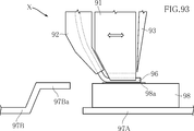
- the bonding tool X includes a wedge 91, a wire guide 92, and a cutter 93.
- the wedge 91, the wire guide 92, and the cutter 93 are supported by a horn (not shown).
- the horn generates ultrasonic vibration in a state where the wedge 91 is pressed against the connection target.
- the wire guide 92 is for guiding the wire 96 to the tip of the wedge 91.
- the wedge 91 joins the wire 96 and the connection target by applying ultrasonic vibration and pressure with the wire 96 sandwiched between the tip and the connection target.
- the cutter 93 cuts the wire 96 that has been connected.
- first bonding is performed on the electrode pad 98a of the semiconductor element 98 mounted on the lead 97A.
- the wire 96 is pressed against the electrode pad 98a to be connected by the wedge 91.
- ultrasonic vibration is applied in this state, the wire 96 is bonded to the electrode pad 98a.
- This joined portion becomes the first bonding portion 96A shown in FIG.
- the bonding tool X is moved directly above the lead 97B, and second bonding is performed.
- ultrasonic vibration is applied while pressing the wire 96 against the pad portion 97Ba, which is the other connection target, by the wedge 91.
- the wire 96 is bonded to the pad portion 97Ba.
- This joined portion becomes a second bonding portion 96B shown in FIG.
- the first bonding portion 96A and the second bonding portion 96B are connected via a bridging portion 96C.
- the electrode 98a of the semiconductor element 98 and the lead 97B can be made conductive.
- the wire 96 a wire made of Al was often used.
- electronic devices called power devices have been developed.
- a large current flows through wires in an electronic device called a power device. Therefore, it is considered to use the wire 96 made of Cu.
- the wire 96 made of Cu has low electrical resistance and thermal resistance, and can efficiently release the heat generated in the semiconductor element 98 to the outside of the electronic device.
- the wire 96 made of Cu is harder than the wire 96 made of Al and is not easily deformed. Therefore, when the wire 96 is pressed against the electrode pad 98a to be connected by the wedge 91, the wire 96 is not deformed so much that an excessive force may be applied to the electrode pad 98a. In such a case, the semiconductor element 98 is damaged.
- the present invention has been conceived under the circumstances described above, and even when a wire made of Cu is used, the wire is appropriately bonded to the bonding target while preventing damage to the electronic element.
- the main object is to provide a method of manufacturing a wire bonding structure that can be bonded.
- the method includes a step of preparing a wire made of Cu, and a step of bonding the wire to a first bonding target formed in an electronic element, before the bonding step.
- the wire has an outer peripheral surface and a retracting surface, and the retracting surface is a surface retracted from the outer peripheral surface to the central axis side of the wire, and in the joining step, the retracting surface is A method of manufacturing a wire bonding structure is provided, in which ultrasonic vibration is applied to the wire in a state of being pressed against the first bonding target.
- the retracting surface is flat when the joining step is started.
- the method further includes a step of forming the retracting surface by pressing the wire against a pressing target before the joining step.
- the pressing object is made of ceramic or metal.
- the method further includes a step of preparing a wedge for pressing the wire, and in the step of forming the retracting surface, the wire is pressed against the pressing target by the wedge and bonded to the first bonding target. In the step, the wire is pressed against the first joining object by the wedge.
- a guide groove for guiding the wire is formed in the wedge, and the wire is inserted into the guide groove between the step of forming the retracting surface and the step of bonding to the first bonding target.
- the wire is pressed against the pressing target by the inner surface of the guide groove, and in the step of bonding to the first bonding target, the wire is connected to the first bonding target by the inner surface of the guide groove. Press against.
- the wire has a circular shape with a diameter of 150 to 1000 ⁇ m.
- the wire has a circular shape with a diameter of 300 to 1000 ⁇ m.
- the wire is entirely made of Cu.
- the method further includes a step of bonding the wire to the second bonding target by applying ultrasonic vibration while the wire is pressed against the second bonding target.
- the electronic element is a semiconductor element.
- the semiconductor element is a MOSFET or an IGBT.
- a first joining object having a first surface
- a second joining object comprising: a first joining object having a first surface; a second joining object; and a wire joined to both the first joining object and the second joining object.
- the wire bonding structure is provided in which the wire is made of Cu and has a circular shape with a diameter of 150 to 1000 ⁇ m.
- the wire has a circular shape with a diameter of 300 to 1000 ⁇ m.
- the wire is entirely made of Cu.
- the wire includes a bonding portion bonded to the first bonding target, and the bonding portion includes an outer peripheral surface and a bonding surface bonded to the first bonding target, and the bonding surface. Is a surface retracted from the outer peripheral surface to the central axis side of the wire.
- the dimension of the joint surface is 60 to 80% of the diameter of the wire
- the first direction is a direction in which the central axis of the wire extends. The direction perpendicular to the direction of the first surface.
- the dimension of the joint surface in the cross-sectional shape orthogonal to the first direction is 90 to 800 ⁇ m.
- the dimension of the joint surface in the first direction is 3 to 10 times the diameter of the wire.
- the size of the joint surface in the first direction is 1200 to 4000 ⁇ m.
- the joint surface has an elliptical shape whose major axis coincides with the direction in which the central axis of the wire extends.
- an elliptical oval mark is formed on the joint surface, and the elliptical mark is located inside an edge of the joint surface.
- the bonding portion has a first pressed surface and a second pressed surface, and the first pressed surface and the second pressed surface are on the central axis side of the wire from the outer peripheral surface.
- the first pressed surface and the second pressed surface are retracted surfaces, and when viewed in a direction orthogonal to the first surface, a virtual plane that passes through the central axis and is orthogonal to the first surface. They are located on opposite sides of each other.
- the first pressed surface and the second pressed surface are inclined with respect to the virtual plane.
- the bonding portion includes a first curve mark formed at a position shifted from an edge of the first pressed surface and a second curve formed at a position shifted from the edge of the second pressed surface. Curve marks are formed.
- the bonding portion is a first bonding portion
- the wire includes a second bonding portion and a bridging portion, and the bridging portion connects the first bonding portion and the second bonding portion.
- the second bonding portion is bonded to the second bonding target.
- An electronic device is provided that is a pad.
- the electronic element is a semiconductor element.
- the semiconductor element is a MOSFET or an IGBT.
- the first joining target is made of Al.
- the thickness of the first joining target is 1 to 10 ⁇ m.
- the maximum current value flowing through the wire is 150 to 200A.
- the first bonding target includes a metal layer and an electrode pad
- the wire is bonded to the metal layer
- the metal layer is interposed between the wire and the electrode pad
- the metal layer is thicker than the electrode pad.
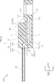
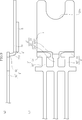
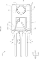
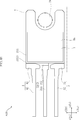
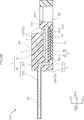
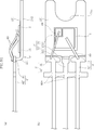
- FIG. 1 is a front view of an electronic device according to a first embodiment of the present invention.
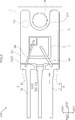
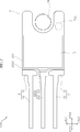
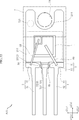
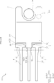
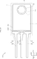
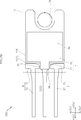
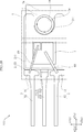
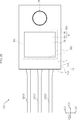
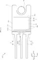
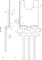
- 1 is a plan view of an electronic device according to a first embodiment of the present invention. It is a bottom view of the electronic device concerning a 1st embodiment of the present invention.
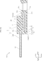
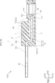
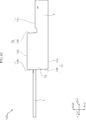
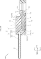
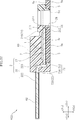
- 1 is a cross-sectional view of an electronic device according to a first embodiment of the present invention.
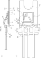
- 1 is a plan view (partially see through) of an electronic device according to a first embodiment of the present invention.
- 1 is a bottom view (partially see through) of an electronic device according to a first embodiment of the present invention.
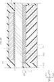
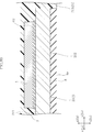
- FIG. 6 is a partial enlarged cross-sectional view of the electronic device shown in FIG. 5.
- A is a front view in 1 process of the manufacturing process of the electronic device concerning 1st Embodiment of this invention.
- (B) is a top view of the structure shown to (a). It is a front view which shows 1 process of the wire bonding method concerning 1st Embodiment of this invention.
- 1 is an overall schematic diagram showing a bonding tool used in a wire bonding method according to a first embodiment of the present invention. It is a perspective view which shows a part of wedge in the bonding tool shown in FIG.
- FIG. 13 is a cross-sectional view taken along line XIII-XIII in FIG. 12. It is a figure which shows one process following FIG. FIG.
- FIG. 15 is a sectional view taken along line XV-XV in FIG. 14. It is the figure which looked at the wire when performing the process shown in FIG. 14 from the downward direction. It is the figure which looked at the wire when performing the process shown in FIG. 14 from upper direction. It is a figure which shows one process following FIG. FIG. 19 is a cross-sectional view taken along line XIX-XIX in FIG. It is a figure which shows one process following FIG. FIG. 21 is a diagram showing one process following FIG. 20.
- FIG. 22 is a diagram showing one process following on from FIG. 21.
- FIG. 23 is a diagram showing one process following on from FIG. 22. It is the elements on larger scale of the wire bonding structure shown in FIG. FIG.
- FIG. 25 is a sectional view taken along line XXV-XXV in FIG. 24. It is a top view of the wire bonding structure shown in FIG.
- FIG. 25 is a bottom view of wires in the wire bonding structure shown in FIG. 24 (other than wires are omitted).
- FIG. 27 is a sectional view taken along line XXVIII-XXVIII in FIG. 26.
- A) is a front view in 1 process of the manufacturing process of the electronic device concerning 1st Embodiment of this invention.
- (B) is a top view of the structure shown to (a). It is a front view (partial sectional view) in one process of a manufacturing process of an electronic device concerning a 1st embodiment of the present invention.
- FIG. 46 It is a front view of the electronic device concerning 2nd Embodiment of this invention. It is a top view of the electronic device concerning 2nd Embodiment of this invention. It is a bottom view of the electronic device concerning 2nd Embodiment of this invention. It is sectional drawing of the electronic device concerning 2nd Embodiment of this invention. It is a top view (partially see-through
- (A) is a front view in one process of the manufacturing process of the electronic device concerning 2nd Embodiment of this invention.
- (B) is a top view of the structure shown to (a).
- (A) is a front view in one process of the manufacturing process of the electronic device concerning 2nd Embodiment of this invention.
- (B) is a top view of the structure shown to (a).
- (A) is a front view in one process of the manufacturing process of the electronic device concerning 2nd Embodiment of this invention.
- (B) is a top view of the structure shown to (a). It is sectional drawing in 1 process of the manufacturing process of the electronic device concerning 2nd Embodiment of this invention. It is sectional drawing of the electronic device concerning the 1st modification of 2nd Embodiment of this invention.
- FIG. 80 is a partial enlarged cross-sectional view of the electronic device shown in FIG. 79.
- A) is a front view in one process of the manufacturing process of the electronic device concerning 3rd Embodiment of this invention.
- B) is a top view of the structure shown to (a).
- A) is a front view in one process of the manufacturing process of the electronic device concerning 3rd Embodiment of this invention.
- B) is a top view of the structure shown to (a).
- FIG. 87 is a partial enlarged cross-sectional view of the electronic device shown in FIG. 87.
- A is a front view in one process of the manufacturing process of the electronic device concerning the 1st modification of 3rd Embodiment of this invention.
- (B) is a top view of the structure shown to (a).
- (A) is a front view in one process of the manufacturing process of the electronic device concerning the 1st modification of 3rd Embodiment of this invention.
- (B) is a top view of the structure shown to (a). It is principal part sectional drawing which shows the modification of the mounting structure of the electronic device concerning 3rd Embodiment of this invention. It is a figure which shows the first bonding process in an example of the conventional wire bonding method. It is a figure which shows the 2nd bonding process in an example of the conventional wire bonding method.
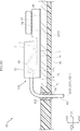
- FIG. 1 is a cross-sectional view of a principal part showing a mounting structure of an electronic device according to the present embodiment.
- the electronic device mounting structure B1 shown in FIG. 1 includes an electronic device A10, a mounting substrate 81, and a heat sink 82.
- the mounting board 81 is a board on which a plurality of electronic components are mounted.
- the mounting substrate 81 is made of an insulating material.
- a wiring pattern (not shown) is formed on the mounting substrate 81.
- a plurality of holes 811 are formed in the mounting substrate 81.
- the heat sink 82 is erected on the mounting substrate 81.
- the heat sink 82 is made of a material having a relatively high thermal conductivity, for example, a metal such as aluminum.
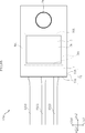
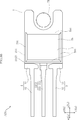
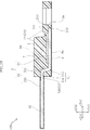
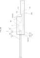
- FIG. 2 is a front view of the electronic device according to the present embodiment.
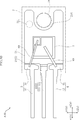
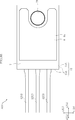
- FIG. 3 is a plan view of the electronic device according to the present embodiment.
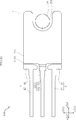
- FIG. 4 is a bottom view of the electronic device according to the present embodiment.
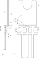
- FIG. 5 is a cross-sectional view of the electronic device according to the present embodiment.
- FIG. 6 is a plan view (partially see through) of the electronic device according to the present embodiment.
- FIG. 7 is a bottom view (partially see through) of the electronic device according to the present embodiment.
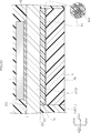
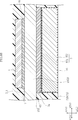
- FIG. 8 is a partial enlarged cross-sectional view of the electronic device shown in FIG.
- the electronic device A10 shown in these drawings includes an electronic element 1, electrodes 2 to 4, a heat radiating member 5, an adhesive layer 61 (see FIG. 8, omitted in other drawings), and a plating layer 62 (FIG. 1, FIG. 5, omitted in other drawings), two wires 69, and a resin package 7. 6 and 7, the resin package 7 is indicated by a two-dot chain line.
- the electronic device A10 is mounted on a mounting board 81.
- the electronic device A10 is used as an electronic component that performs a switching function, a rectifying function, an amplifying function, and the like in an electric circuit depending on the type of the electronic element 1.
- the electronic element 1 shown in FIGS. 1, 5, and 6 has a rectangular shape in plan view.
- the electronic element 1 is an element made of a semiconductor such as a diode or a transistor.
- the electronic element 1 is a transistor.
- examples of the electronic element 1 include a MOSFET (Metal Oxide Semiconductor Field Effect Transistor) and an IGBT (Insulated Gate Bipolar Transistor).
- MOSFET Metal Oxide Semiconductor Field Effect Transistor
- IGBT Insulated Gate Bipolar Transistor
- the electrode 2 includes a die bonding pad 21 and a lead 22.
- the die bonding pad 21 and the lead 22 are made of a conductive material such as copper, for example.
- the die bonding pad 21 and the lead 22 are integrally molded.
- the die bonding pad 21 and the lead 22 are formed by integrally molding a conductive member having a uniform thickness, for example, by bending.
- the die bonding pad 21 is for mounting the electronic element 1.
- the die bonding pad 21 has a flat plate shape extending in the xy plane.
- the die bonding pad 21 has an arrangement surface 211 and a back surface 212.
- the arrangement surface 211 faces the direction z1.
- the back surface 212 faces the direction z2.
- the electronic element 1 is arranged on the arrangement surface 211. Heat generated in the electronic element 1 is transmitted to the die bonding pad 21.
- the die bonding pad 21 has a hole 214 penetrating from the arrangement surface 211 to the back surface 212. As shown in FIG. 6, the hole 214 has a concave shape that is recessed in the x1 direction from the end on the direction x2 side of the die bonding pad 21 in the xy plan view.
- the lead 22 has a shape extending linearly from the die bonding pad 21.
- the lead 22 is for insertion mounting. As shown in FIG. 1, the lead 22 is inserted into the hole 811. As a result, the electronic device A10 is mounted on the mounting substrate 81. In order to fix the lead 22 to the mounting substrate 81, the hole 811 is filled with solder 84.
- the lead 22 has a connecting portion 221 and a terminal portion 222.
- the connecting part 221 is connected to the die bonding pad 21.
- the connecting portion 221 extends from the die bonding pad 21 in a direction intersecting with the arrangement surface 211.
- the terminal part 222 is connected to the connecting part 221.
- the terminal portion 222 extends from the connecting portion 221 in the direction x1.
- the terminal portion 222 has a portion protruding from the resin package 7 described later.
- the lead 22 is formed by integrally molding a conductor member having a uniform thickness together with the die bonding pad 21. Therefore, as shown in FIG. 5, the thickness L ⁇ b> 2 (dimension in the direction z) of the terminal portion 222 protruding from the resin package 7 is the same as the thickness L ⁇ b> 1 (dimension in the direction z) of the die bonding pad 21. is there.
- the electrode 3 includes a wire bonding pad 31 and a lead 32.
- the electrode 3 is located on the direction x1 side of the die bonding pad 21 and on the direction y1 side of the lead 22 in the xy plan view.
- the wire bonding pad 31 and the lead 32 are integrally molded.
- the wire bonding pad 31 and the lead 32 are made of a conductive material such as copper, for example.
- the wire bonding pad 31 has a substantially rectangular flat plate shape smaller than the die bonding pad 21.
- the lead 32 is connected to the wire bonding pad 31.
- the lead 32 has a shape extending linearly from the wire bonding pad 31 toward the direction x1.
- the lead 32 is in parallel with the lead 22.
- the lead 32 has a portion protruding from a resin package 7 described later.
- the lead 32 is for insertion mounting. As shown in FIG. 1, the lead 32 is inserted into the hole 811. As a result, the electronic device A10 is mounted on the mounting substrate 81. In order to fix the lead 32 to the mounting substrate 81, the hole 811 is filled with solder 84.
- the electrode 4 includes a wire bonding pad 41 and a lead 42.
- the electrode 4 is located on the direction x1 side of the die bonding pad 21 and on the direction y2 side of the lead 22 in the xy plan view.
- the wire bonding pad 41 and the lead 42 are integrally molded.
- the wire bonding pad 41 and the lead 42 are made of a conductive material such as copper, for example.
- the wire bonding pad 41 has a substantially rectangular flat plate shape smaller than the die bonding pad 21.
- the lead 42 is connected to the wire bonding pad 41.
- the lead 42 has a shape extending linearly from the wire bonding pad 41 in the direction x1.
- the lead 42 is parallel to the lead 22.
- the lead 22 is located between the lead 42 and the lead 32.
- the lead 42 has a portion protruding from a resin package 7 described later.
- the lead 42 is for insertion mounting. As shown in FIG. 1, the lead 42 is inserted into the hole 811. As a result, the electronic device A10 is mounted on the mounting substrate 81. In order to fix the lead 42 to the mounting substrate 81, the hole 811 is filled with solder 84.
- the adhesive layer 61 is interposed between the electronic element 1 and the die bonding pad 21.
- the adhesive layer 61 is for bonding the electronic element 1 to the die bonding pad 21.
- the electronic element 1 is electrically connected to the die bonding pad 21 through the adhesive layer 61.
- the adhesive layer 61 is, for example, a silver paste or a solder paste.
- the heat radiating member 5 is disposed on the opposite side to the side on which the electronic element 1 is disposed with the die bonding pad 21 interposed therebetween. That is, the die bonding pad 21 is located between the heat dissipation member 5 and the electronic element 1.
- the heat radiating member 5 is located on the side of the direction x1 from the hole 214.
- the heat radiating member 5 has a substantially rectangular plate shape. When the heat radiating member 5 has a substantially rectangular plate shape, it is not necessary to perform a special process such as making a hole to form the heat radiating member 5, so that the heat radiating member 5 is easy to manufacture.
- the heat dissipation member 5 may be bonded to the die bonding pad 21 via an adhesive, but in the present embodiment, the heat radiating member 5 is bonded to the die bonding pad 21 by ultrasonic bonding. Therefore, no adhesive or the like is interposed between the heat radiating member 5 and the die bonding pad 21, and the heat radiating member 5 and the die bonding pad 21 are in direct contact with each other.
- the heat dissipation member 5 is provided in order to quickly release the heat generated in the electronic element 1 to the outside of the electronic device A10. In order to quickly release the heat generated in the electronic element 1 to the outside of the electronic device A10, the higher the thermal conductivity of the material constituting the heat radiating member 5, the better.
- the heat radiating member 5 is made of a material having a higher thermal conductivity than that of the material constituting the resin package 7. More preferably, the heat radiating member 5 is made of a material having a thermal conductivity higher than that of the material constituting the die bonding pad 21.
- the heat radiating member 5 is made of a conductor such as aluminum, copper, or iron. In addition, the heat radiating member 5 may be made of aluminum plated with silver.
- the resin package 7 shown in FIGS. 1 to 8 covers the electronic element 1, the electrodes 2 to 4, and the heat radiating member 5.
- the resin package 7 is made of, for example, a black epoxy resin.
- the resin package 7 has a first surface 71 and a second surface 72.
- the first surface 71 has a flat surface 715 and a tapered surface 716.
- the flat surface 715 faces the heat sink 82.
- Grease 89 may be interposed between the flat surface 715 and the heat sink 82. Or although not shown in figure, the flat surface 715 and the heat sink 82 may contact
- the tapered surface 716 is connected to the flat surface 715.
- the taper surface 716 has a shape toward the outside in the xy plane as it goes in the direction z1. As shown in FIG. 4, pin marks 711 that are recessed from the flat surface 715 are formed in the resin package 7.
- the second surface 72 has a plurality of flat surfaces 725 and a plurality of tapered surfaces 726.
- Each tapered surface 726 is connected to one of the plurality of flat surfaces 725.
- Each tapered surface 726 has a shape toward the outside in the xy plane as it goes in the direction z2.
- Each tapered surface 726 is connected to the tapered surface 716 at the boundary 73.
- pin traces 721 that are recessed from the flat surface 725 are formed in the resin package 7.
- screw holes 78 are formed in the resin package 7.
- a screw 83 for fixing the electronic device A ⁇ b> 10 to the heat radiating plate 82 is inserted into the screw hole 78.
- Each wire 69 shown in FIGS. 5 and 6 is made of a metal such as aluminum, for example.
- One of the two wires 69 is bonded to the electronic element 1 and the wire bonding pad 31. Thereby, the electronic element 1 and the wire bonding pad 31 are conducted.
- One of the two wires 69 is bonded to the electronic element 1 and the wire bonding pad 41. Thereby, the electronic element 1 and the wire bonding pad 41 are conducted.
- the wire 69 need not be bonded to either of the wire bonding pads 31 and 41. In this case, the wire 69 may be bonded to either one of the wire bonding pads 31 and 41.
- the plated layer 62 shown in FIGS. 1 and 5 covers the portions of the leads 22, 32, 42 protruding from the resin package 7.
- the plated layer 62 is made of an alloy of tin, silver and copper, for example.
- electrodes 2 ', 3' and 4 ' are formed.
- the heat radiating member 5 is bonded to the die bonding pad 21 of the electrode 2 '.
- the die bonding pad 21 and the heat dissipation member 5 are joined by ultrasonic joining.
- the electronic element 1 is disposed on the die bonding pad 21 through an adhesive layer 61 (see FIG. 8, omitted in FIG. 29). The position where the electronic element 1 is disposed is opposite to the heat dissipation member 5 with the die bonding pad 21 interposed therebetween.
- the wire 69 is bonded to the electronic element 1 and the wire bonding pad 31. Similarly, the wire 69 is bonded to the electronic element 1 and the wire bonding pad 41.
- the bonding of the wire 69 is performed as follows using the following bonding tool 900A.
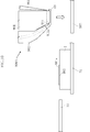
- FIG. 10 is a front view showing one step of the wire bonding method according to the first embodiment of the present invention.
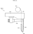
- FIG. 11 is an overall schematic view showing a bonding tool used in the wire bonding method according to the first embodiment of the present invention.
- the bonding tool 900A shown in these drawings includes a wedge 901, a wire guide 902, a cutter 903, a main body 904, and a horn 905.
- the bonding tool 900A is used for bonding the wire 69 to a bonding target.
- the horn 905 holds the wedge 901 and is for applying ultrasonic vibration while pressing the wedge 901 against the object to be joined.
- the horn 905 is supported by the main body 904.
- the horn 905 is fixed to the main body 904 via an elastic support member (not shown). Thereby, the horn 905 is elastically supported by the main body 904.
- the wire guide 902 is fixed to the wedge 901, and is for guiding the wire 69 from the wire reel 965 to the wedge 901, for example.
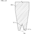
- FIG. 12 is a perspective view showing a part of the wedge in the bonding tool shown in FIG. 13 is a cross-sectional view taken along line XIII-XIII in FIG.
- the wedge 901 is a portion that presses the wire 69 and is bonded to a bonding target by ultrasonic vibration.
- the wedge 901 is made of, for example, tungsten carbide.
- a guide groove 911 is formed in the wedge 901.
- the guide groove 911 is provided at the lower end of the wedge 901.
- the guide groove 911 has a V-shaped cross section.
- the cutter 903 is for cutting the wire 69 and is disposed adjacent to the wedge 901. In the present embodiment, the cutter 903 is rigidly attached to the main body 904.
- the cross-sectional shape of the wire 69 used in this embodiment is circular.
- the wire 69 has a circular shape with a diameter of 150 to 1000 ⁇ m. More preferably, the wire 69 has a circular shape with a diameter of 200 to 1000 ⁇ m. More preferably, the wire 69 has a circular shape with a diameter of 300 to 1000 ⁇ m.
- the wire 69 is made of Cu. Preferably, the wire 69 is entirely made of Cu.
- FIG. 10 changes from a state wound around the wire reel 965 by being deformed or cut.
- the wire is shown as the wire 69 in any scene.
- the tip of the wedge 901 of the bonding tool 900A that is ready to start the wire bonding method is positioned immediately above the pressing object 982. Then, the tip of the wedge 901 is directed toward the pressing object 982. At this time, the distal end portion of the wire 69 is fitted in the guide groove 911.
- the pressing object 982 is made of, for example, ceramic or metal. In the present embodiment, the surface of the pressing object 982 is flat. Further, the pressing object 982 may be a part of the electrode 2 or the electrode 3, for example.
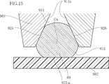
- the wire 69 is pressed against the surface of the pressing object 982 by the wedge 901. Specifically, the wire 69 is pressed against the surface of the pressing target 982 by the inner surface 911 a of the guide groove 911.
- FIG. 15 is a sectional view taken along line XV-XV in FIG.
- FIG. 16 is a view of the wire as viewed from below when the process shown in FIG. 14 is performed.
- FIG. 17 is a view of the wire as viewed from above when the process shown in FIG. 14 is performed. 16 and 17, the wedge 901 is not shown, and in FIG. 16, the pressing target 982 is shown using virtual lines.
- the retraction surface 923 ⁇ is formed by pressing the wire 69 against the pressing object 982.
- the retracting surface 923 ⁇ is a portion that has been in contact with the pressing object 982 at the time of pressing.
- the retreat surface 923 ⁇ is a surface retreated from the outer peripheral surface 921 having an arcuate cross section toward the central axis Ox of the wire 69.
- the retracting surface 923 ⁇ is flat.
- FIGS. 15 and 17 when the wire 69 is pressed against the pressing target 982, a first pressed surface 925 and a second pressed surface 926 are formed.
- the first pressed surface 925 and the second pressed surface 926 are portions that are pressed against the inner surface 911 a of the guide groove 911.
- the first pressed surface 925 and the second pressed surface 926 are surfaces that are retracted from the outer peripheral surface 921 having an arcuate cross section toward the central axis Ox of the wire 69.
- the wedge while maintaining the state in which the wire 69 is disposed in the guide groove 911, the wedge extends from a position where the guide groove 911 directly faces the pressing object 982 to a position where the guide groove 911 faces the electrode pad 981. 901 is moved. Then, the tip of the wedge 901 is directed toward the electrode pad 981. At this time, the tip portion of the wire 69 remains in the guide groove 911.
- the wire 69 is bonded to the electrode pad 981 formed on the electronic element 1.
- the electrode pad 981 corresponds to an example of a first bonding target referred to in the present invention.
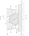
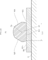
- ultrasonic vibration is applied to the wire 69 while the retracting surface 923 ⁇ is pressed against the electrode pad 981. More specifically, when bonding the wire 69 to the electrode pad 981, the wire 69 is pressed against the electrode pad 981 by the wedge 901. More specifically, the wire 69 is pressed against the electrode pad 981 by the inner surface 911a of the guide groove 911. As a result, the wire 69 is further crushed. Then, the wire 69 and the electrode pad 981 are ultrasonically welded. This welded portion is the first bonding portion 906A, and the surface of the wire 69 that is bonded to the electrode pad 981 is the bonding surface 923.
- a second bonding process is performed.
- the wire 69 is bonded to the wire bonding pad 31.
- the wire bonding pad 31 corresponds to an example of a second bonding target referred to in the present invention.
- ultrasonic vibration is applied with the wire 69 pressed against the wire bonding pad 31.
- the wire 69 and the wire bonding pad 31 are ultrasonically welded. This welded portion becomes the second bonding portion 906B.
- the bonding tool 900A is moved to the left in the figure.
- the cutter 903 is positioned between the left end of the second bonding portion 906B in the drawing and the left end of the wire bonding pad 31 in the drawing.
- the cutter 903 rigidly attached to the main body 904 is lowered together with the main body 904.
- the wire 69 is cut by the lowering of the cutter 903. That is, the lowering amount of the main body 904 is set to such an extent that the cutter 903 does not completely cut the wire 69.
- the wire 69 is separated from the wire bonding pad 31 together with the wedge 901. As a result, the cut wire 69 is cut.
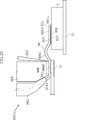
- the wire bonding structure 900B shown in the figure includes a wire 69, an electrode pad 981, and a wire bonding pad 31.
- FIG. 24 is a partially enlarged view of the wire bonding structure shown in FIG.
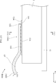
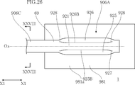
- FIG. 25 is a sectional view taken along line XXV-XXV in FIG. 26 is a plan view of the wire bonding structure shown in FIG.
- FIG. 27 is a bottom view of the wire in the wire bonding structure shown in FIG. 24 (except for the wire is omitted).
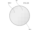
- FIG. 28 is a sectional view taken along line XXVIII-XXVIII in FIG.
- the electrode pad 981 and the wire bonding pad 31 are made of a conductive material.
- An example of such a material is Al.
- Each of the electrode pad 981 and the wire bonding pad 31 may have a structure in which a plurality of metal layers made of different metals are laminated.
- the electrode pad 981 and the wire bonding pad 31 are, for example, an electrode pad or a lead frame.
- the electrode pad 981 is an electrode pad
- the wire bonding pad 31 is a lead frame.
- the thickness of the electrode pad 981 that is an electrode pad is, for example, 1 to 10 ⁇ m.
- the electrode pad 981 has a first surface 981a.
- the wire 69 is bonded to both the electrode pad 981 and the wire bonding pad 31.
- the wire 69 includes a first bonding portion 906A, a second bonding portion 906B, and a bridging portion 906C.
- the first bonding portion 906A is bonded to the electrode pad 981. Specifically, the first bonding portion 906A is bonded to the first surface 981a of the electrode pad 981.
- the first bonding portion 906 ⁇ / b> A has an outer peripheral surface 921, a bonding surface 923, a first pressed surface 925, and a second pressed surface 926.
- the bonding surface 923 has an elliptical shape whose major axis coincides with the direction in which the central axis Ox of the wire 69 extends.
- An elliptical scar 923 ⁇ / b> C may be formed on the bonding surface 923.
- the ellipse mark 923C is located inside the edge 923B of the joint surface 923.
- the ellipse mark 923C is formed when the edge of the retracting surface 923 ⁇ shown in FIGS. 15 and 16 is harder than other portions by work hardening of the metal. Unlike the present embodiment, the ellipse mark 923 ⁇ / b> C may not be formed on the joint surface 923.
- the direction in which the central axis Ox of the wire 69 extends and is perpendicular to the direction in which the first surface 981a faces is defined as the first direction X1.
- the dimension L11 (see FIGS. 25 and 27) of the bonding surface 923 in the cross-sectional shape by the cross section orthogonal to the first direction X1 is, for example, 60 to 80% of the diameter of the wire 69.
- the diameter of the wire 69 means the diameter of a circular bridge 906C described later.
- the dimension L11 (see FIGS. 25 and 27) of the joint surface 923 in the cross-sectional shape orthogonal to the first direction X1 is, for example, 90 to 800 ⁇ m.
- a dimension L12 (see FIG. 27) of the joint surface 923 in the first direction X1 is, for example, 1200 to 4000 ⁇ m.
- the first pressed surface 925 and the second pressed surface 926 shown in FIGS. 24 to 26 are surfaces retracted from the outer peripheral surface 921 to the center axis Ox side of the wire 69.
- the first pressed surface 925 and the second pressed surface 926 are virtual planes that pass through the central axis Ox and are orthogonal to the first surface 981a when viewed in a direction orthogonal to the first surface 981a. They are located on opposite sides of P1.
- the first pressed surface 925 and the second pressed surface 926 are inclined with respect to the virtual plane P1.
- the position of the inner surface 911a of the guide groove 911 with respect to the first pressed surface 925 and the second pressed surface 926 is determined by the step of pressing the wire 69 against the pressing target 982 (see FIGS. 14 and 15). During the bonding process 69 (see FIGS. 18 and 19), there is a possibility that the position is slightly shifted. In this case, as shown in FIG. 26, when the wire 69 is bonded to the electrode pad 981, the inner surface 911 a of the guide groove 911 presses the wire 69, whereby the first curve mark 927 and the second curve mark 928 are pressed against the wire 69. May be formed.
- the first curve mark 927 is formed at a position shifted from the edge 925 ⁇ / b> B of the first pressed surface 925.
- the second curve mark 928 is formed at a position shifted from the edge 926 ⁇ / b> B of the second pressed surface 926.
- the first curve mark 927 and the second curve mark 928 may not be formed on the wire 69.
- FIG. 23 is a part bonded to the wire bonding pad 31 in the wire 69.
- a bridging portion 906C shown in FIGS. 23 and 24 connects the first bonding portion 906A and the second bonding portion 906B.
- the cross-sectional shape of the bridging portion 906C is circular.
- the electrode pad 981 of the wire bonding structure 900B is laminated on the electronic element 1.
- the wire 69 is bonded to the wire bonding pad 31 and the electronic element 1. Although not described in detail, similarly, the wire 69 is bonded to the wire bonding pad 41 and the electronic element 1. In this way, the configuration shown in FIG. 29 can be obtained.
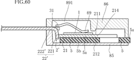
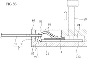
- the leads 22 ', 32', and 42 ' are sandwiched between the mold 85 and the mold 86 (only the lead 42' is shown in FIG. 30).
- the molds 85 and 86 are fixed to the leads 22 ′, 32 ′, and 42 ′ with the molds 85 and 86 sandwiching the leads 22 ′, 32 ′, and 42 ′.
- the die bonding pad 21 is fixed to the molds 85 and 86 using the pins 87 and 88.
- a space 891 surrounded by the mold 85 and the mold 86 is formed.
- the space 891 accommodates the die bonding pad 21, the electronic element 1, and the like.
- the portion of the resin package 7 where the pin 87 has been inserted becomes the pin mark 711 described above. Similarly, the portion of the resin package 7 where the pin 88 is inserted becomes the above-described pin mark 721. Thereafter, the leads 22 ', 32', and 42 'are cut along the line 899 (see FIG. 29), and the electronic device A10 is manufactured.
- the electronic device A10 includes the wire bonding structure 900B described above.
- the other electronic devices described below are also common in that the wire bonding structure 900B is included in the same manner.
- the wire 69 before the step of bonding the wire 69 to the electrode pad 981, the wire 69 has a retracting surface 923 ⁇ .
- the retreat surface 923 ⁇ is a surface retreated from the outer peripheral surface 921 to the center axis Ox side of the wire 69.
- ultrasonic vibration is applied to the wire 69 in a state where the retracting surface 923 ⁇ is pressed against the electrode pad 981.
- the wire 69 when the wire 69 is pressed against the electrode pad 981 by the wedge 901, it is possible to suppress a local force from being applied to the electrode pad 981 from the wire 69. As a result, it is possible to prevent the electronic element 1 on which the electrode pad 981 is formed from being damaged. As described above, according to the present embodiment, even when the wire 69 made of Cu is used, the wire 69 can be appropriately bonded to the electrode pad 981 while preventing damage to the electronic element 1.
- the retracting surface 923 ⁇ is flat when the process of bonding the wire 69 to the electrode pad 981 is started. According to such a configuration, when the wire 69 is bonded to the electrode pad 981, when the wire 69 is pressed against the electrode pad 981 by the wedge 901, the area of the wire 69 in contact with the electrode pad 981 can be further increased. it can. Therefore, for the same reason as described above, even when the wire 69 made of Cu is used, the wire 69 can be more appropriately bonded to the electrode pad 981 while further preventing the electronic element 1 from being damaged.
- the retraction surface 923 ⁇ is formed by pressing the wire 69 against the pressing object 982 before joining the wire 69 to the electrode pad 981.
- Such a configuration is suitable for forming the retracting surface 923 ⁇ on the wire 69.
- the wire 69 in which the retracting surface 923 ⁇ is already formed from the time when it is wound around the wire reel 965 may be used. In this case, it is not necessary to perform the step of forming the retracting surface 923 ⁇ by pressing the wire 69 against the pressing object 982.
- the wire 69 As the diameter of the wire 69 is larger, in order to join the wire 69 and the electrode pad 981, it is necessary to press the wire 69 against the electrode pad 981 with a larger force.
- the wire 69 having a diameter of about 150 to 1000 ⁇ m and having a large diameter is used.
- the wire 69 can be appropriately bonded to the electrode pad 981 while preventing the electronic element 1 from being damaged.
- the electronic device A10 includes a heat dissipation member 5. Therefore, the heat transferred from the electronic element 1 to the die bonding pad 21 can be conducted to the heat radiating plate 82 through the heat radiating member 5. Therefore, the heat transferred from the electronic element 1 to the die bonding pad 21 is easily transferred to the heat radiating plate 82. Therefore, the electronic device A10 is suitable for suppressing the electronic element 1 from becoming excessively high in temperature. That is, the electronic device A10 is excellent in heat dissipation.
- the electrode 2 is formed by molding a conductive member having a uniform thickness. Therefore, it is not necessary to use a conductive member in which the thickness of the die bonding pad 21 and the thickness of the lead 22 are different in order to form the electrode 2.
- a conductive member having a uniform thickness can be manufactured at low cost. Therefore, the electronic device A10 is suitable for reducing the manufacturing cost.
- the die bonding pad 21 and the heat radiating member 5 are bonded by ultrasonic bonding.
- the die bonding pad 21 is not easily oxidized when the heat dissipation member 5 is bonded. That is, even after the heat dissipation member 5 is bonded, the arrangement surface 211 of the die bonding pad 21 is not covered with the oxide film, and the conductive material can be kept exposed. Therefore, the electronic device A10 is suitable for more reliably conducting the die bonding pad 21 and the electronic element 1.
- the wire 69 does not have the retracting surface 923 ⁇ before the step of bonding the wire 69 to the first bonding target 981A.
- the first joining target 981A is different from the first embodiment in that it includes a metal layer 980 and an electrode pad 981. Since the description of the electrode pad 981 described in the first embodiment can be applied to the electrode pad 981 as it is, description thereof is omitted in this embodiment.
- the metal layer 980 is interposed between the electrode pad 981 and the first bonding portion 906A.
- the metal layer 980 is thicker than the electrode pad 981. The thickness of the metal layer 980 is, for example, 50 to 150 ⁇ m.
- the metal layer 980 serves as a buffer layer. Therefore, it is possible to prevent a local force from being applied to the electrode pad 981. As a result, it is possible to prevent the electronic element 1 on which the first joining target 981A is formed from being damaged. As described above, according to the present embodiment, even when the wire 69 made of Cu is used, the wire 69 can be appropriately bonded to the first bonding target 981A while preventing the electronic element 1 from being damaged.
- FIG. 32 is a cross-sectional view of an electronic device according to this modification.
- FIG. 33 is a plan view (partially see through) of the electronic device according to this variation.
- FIG. 34 is a bottom view (partially see through) of the electronic device according to this variation.
- the electronic device A11 shown in these drawings includes the electronic element 1, the electrodes 2 to 4, the heat radiating member 5, the adhesive layer 61 (see FIG. 8, not shown in this modification), A plated layer 62, two wires 69, and a resin package 7 are provided.
- the electronic device A11 is different from the electronic device A10 in the shape of the heat dissipation member 5.
- Each configuration of the electronic element 1, the electrodes 2 to 4, the adhesive layer 61, the plating layer 62, the wire 69, and the resin package 7 in the electronic device A11 is the same as the configuration of the electronic device A10, and thus the description thereof is omitted.
- the heat dissipation member 5 includes a flat plate portion 51 and a protruding portion 52.
- the flat plate portion 51 has a substantially rectangular plate shape.
- the flat plate portion 51 overlaps the die bonding pad 21 in the xy plan view.
- the protruding portion 52 protrudes from the flat plate portion 51 in the direction x1.
- the protrusion 52 overlaps the lead 22 in the xy plan view.
- a gap 39 is formed between the protrusion 52 and the wire bonding pad 31.
- a gap 49 is formed between the protrusion 52 and the wire bonding pad 41.
- the tip of the protrusion 52 on the direction x1 side is located on the direction x1 side with respect to the die bonding pad 21.
- the heat radiating member 5 includes a protruding portion 52 protruding from the flat plate portion 51.
- the structure in which the heat radiating member 5 includes the protrusion 52 is suitable for increasing the area of the heat radiating member 5 in the xy plan view. Therefore, according to the electronic device A11, heat is easily transmitted from the die bonding pad 21 to the heat dissipation plate 82 via the heat dissipation member 5.
- a gap 39 is formed between the protrusion 52 and the wire bonding pad 31 in the xy plan view. According to such a configuration, it is possible to reduce a region where the protrusion 52 overlaps the wire bonding pad 31 in the xy plan view.
- a heater (not shown) is disposed on the direction z2 side of the wire bonding pad 31.
- the heater is easily disposed. Therefore, according to the electronic device A11, the wire 69 can be easily bonded to the wire bonding pad 31. For the same reason, according to the electronic device A11, the wire 69 can be easily bonded to the wire bonding pad 41.
- FIG. 35 is a cross-sectional view of an electronic device according to this modification.
- FIG. 36 is a plan view (partially see through) of the electronic device according to this variation.
- FIG. 37 is a bottom view (partially see through) of the electronic device according to this variation.
- the electronic device A12 shown in these drawings includes the electronic element 1, the electrodes 2 to 4, the heat radiating member 5, the adhesive layer 61 (see FIG. 8, not shown in this modification), A plated layer 62, two wires 69, and a resin package 7 are provided.
- the electronic device A12 is different from the electronic device A10 in the shape of the heat dissipation member 5.
- Each configuration of the electronic element 1, the electrodes 2 to 4, the adhesive layer 61, the plating layer 62, the wire 69, and the resin package 7 in the electronic device A12 is the same as the configuration of the electronic device A10, and thus the description thereof is omitted.
- a circular screw hole 54 for screw insertion is formed in the heat radiating member 5.
- the heat radiating member 5 has a part located on the side of the direction x2 from the die bonding pad 21.
- the electronic device A12 is suitable for increasing the area of the heat dissipation member 5 in the xy plan view. Therefore, according to the electronic device A12, heat is easily transmitted from the die bonding pad 21 to the heat dissipation plate 82 via the heat dissipation member 5.
- the structure provided with the flat plate part 51 and the protrusion part 52 in the electronic apparatus A11 may be sufficient as the heat radiating member 5 in this modification.
- FIG. 38 is a cross-sectional view of an electronic device according to this modification.
- FIG. 39 is a plan view (partially see through) of the electronic device according to this variation.
- FIG. 40 is a bottom view (partially see through) of the electronic device according to this variation.
- the electronic device A13 shown in these drawings includes the electronic element 1, the electrodes 2 to 4, the heat radiating member 5, the adhesive layer 61 (see FIG. 8, not shown in this modification), A plated layer 62, two wires 69, and a resin package 7 are provided.
- the electronic device A13 is different from the electronic device A10 in the shape of the heat dissipation member 5.
- Each configuration of the electronic element 1, the electrodes 2 to 4, the adhesive layer 61, the plating layer 62, the wire 69, and the resin package 7 in the electronic device A12 is the same as the configuration of the electronic device A10, and thus the description thereof is omitted.
- the heat radiation member 5 is formed with a recess 55 that is recessed from the end in the direction x2 toward the direction x1.
- the recess 55 is open on the direction x2 side.
- the recess 55 overlaps the hole 214 in the die bonding pad 21.
- the heat radiating member 5 has a part located on the side of the direction x2 from the die bonding pad 21.
- the electronic device A13 is suitable for increasing the area of the heat dissipation member 5 in the xy plan view. Therefore, according to the electronic device A13, heat is easily transmitted from the die bonding pad 21 to the heat dissipation plate 82 via the heat dissipation member 5.
- the structure provided with the flat plate part 51 and the protrusion part 52 in the electronic apparatus A11 may be sufficient as the heat radiating member 5 in this modification.
- FIG. 41 is a cross-sectional view of a principal part of the mounting structure of the electronic device according to this modification.
- the electronic device mounting structure B ⁇ b> 2 shown in the figure includes an electronic device A ⁇ b> 10, a mounting substrate 81, and a heat sink 82.
- the electronic device mounting structure B2 is different from the electronic device mounting structure B1 in that a heat sink 82 is formed in parallel with the mounting substrate 81.
- the electronic device A10 is mounted on the mounting substrate 81 with all the leads 22, 32, and 42 bent. Instead of the electronic device A10, any of the electronic devices A11 to A13 may be mounted on the mounting substrate 81.
- FIG. 42 is a cross-sectional view of a principal part showing the mounting structure of the electronic device according to the present embodiment.
- the mounting board 81 is a board on which a plurality of electronic components are mounted.
- the mounting substrate 81 is made of an insulating material.
- a wiring pattern (not shown) is formed on the mounting substrate 81.
- a plurality of holes 811 are formed in the mounting substrate 81.
- the heat sink 82 is erected on the mounting substrate 81.
- the heat sink 82 is made of a material having a relatively high thermal conductivity, for example, a metal such as aluminum.
- FIG. 43 is a front view of the electronic device according to the present embodiment.
- FIG. 44 is a plan view of the electronic device according to the present embodiment.
- FIG. 45 is a bottom view of the electronic device according to the present embodiment.
- FIG. 46 is a cross-sectional view of the electronic device according to the present embodiment.
- FIG. 47 is a plan view (partially see through) of the electronic device according to the present embodiment.
- FIG. 48 is a bottom view (partially see through) of the electronic device according to the present embodiment. 49 is a partial enlarged cross-sectional view of the electronic device shown in FIG.
- the electronic device A20 shown in these drawings includes an electronic element 1, electrodes 2 to 4, a heat radiating member 5, an adhesive layer 61 (see FIG. 49, omitted in other drawings), and a plated layer 62 (FIG. 42, FIG. 46, omitted in other drawings), a bonding layer 63 (see FIG. 49, omitted in other drawings), two wires 69, and a resin package 7. 47 and 48, the resin package 7 is indicated by a two-dot chain line.
- the electronic device A20 is mounted on a mounting board 81.
- the electronic device A20 is used as an electronic component that performs a switching function, a rectifying function, an amplifying function, and the like in an electric circuit depending on the type of the electronic element 1.
- the electronic element 1 has a rectangular shape in plan view.
- the electronic element 1 is an element made of a semiconductor such as a diode or a transistor.
- the electronic element 1 is a transistor.
- the electrode 2 shown in FIGS. 42 and 46 to 48 includes a die bonding pad 21 and a lead 22.
- the die bonding pad 21 and the lead 22 are made of a conductive material such as copper, for example.
- the die bonding pad 21 is for mounting the electronic element 1.
- the die bonding pad 21 has a flat plate shape.
- the die bonding pad 21 has an arrangement surface 211 and a back surface 212.
- the arrangement surface 211 faces the direction z1.
- the back surface 212 faces the direction z2.
- the electronic element 1 is arranged on the arrangement surface 211. Heat generated in the electronic element 1 is transmitted to the die bonding pad 21.
- the die bonding pad 21 has a hole 214 penetrating from the arrangement surface 211 to the back surface 212. As shown in FIG. 47, the hole 214 has a shape that is recessed in the x1 direction from the end on the direction x2 side of the die bonding pad 21 in the xy plan view.
- the lead 22 has a shape extending linearly from the die bonding pad 21.
- the lead 22 is for insertion mounting. As shown in FIG. 42, the lead 22 is inserted into the hole 811. As a result, the electronic device A20 is mounted on the mounting substrate 81. In order to fix the lead 22 to the mounting substrate 81, the hole 811 is filled with solder 84.
- the lead 22 has a joint portion 223 and a terminal portion 222. In the present embodiment, the joint portion 223 and the terminal portion 222 are integrally molded.
- the bonding part 223 is bonded to the die bonding pad 21.
- the joint portion 223 has a shape that extends in a direction intersecting the arrangement surface 211. As shown in FIG.
- the bonding portion 223 has a portion located on the direction z ⁇ b> 2 side with respect to the back surface 212 of the die bonding pad 21. That is, the tip of the bonding portion 223 on the direction z2 side is located on the direction z2 side of the back surface 212 of the die bonding pad 21.
- the terminal part 222 is connected to the joint part 223.
- the terminal portion 222 extends from the joint portion 223 in the direction x1.
- the terminal portion 222 has a portion that protrudes from a resin package 7 described later.
- the 47 and 48 includes a wire bonding pad 31 and a lead 32.
- the electrode 3 is located on the direction x1 side of the die bonding pad 21 and on the direction y1 side of the lead 22 in the xy plan view.
- the wire bonding pad 31 and the lead 32 are integrally molded.
- the wire bonding pad 31 and the lead 32 are made of a conductive material such as copper, for example.
- the wire bonding pad 31 has a substantially rectangular flat plate shape smaller than the die bonding pad 21.
- the lead 32 is connected to the wire bonding pad 31.
- the lead 32 has a shape extending linearly from the wire bonding pad 31 toward the direction x1.
- the lead 32 is in parallel with the lead 22.
- the lead 32 has a portion protruding from a resin package 7 described later.
- the lead 32 is for insertion mounting. As shown in FIG. 42, the lead 32 is inserted into the hole 811. As a result, the electronic device A20 is mounted on the mounting substrate 81. In order to fix the lead 32 to the mounting substrate 81, the hole 811 is filled with solder 84.
- the 47 and 48 includes a wire bonding pad 41 and a lead 42.
- the electrode 4 is located on the direction x1 side of the die bonding pad 21 and on the direction y2 side of the lead 22 in the xy plan view.
- the wire bonding pad 41 and the lead 42 are integrally molded.
- the wire bonding pad 41 and the lead 42 are made of a conductive material such as copper, for example.
- the wire bonding pad 41 has a substantially rectangular flat plate shape smaller than the die bonding pad 21.
- the lead 42 is connected to the wire bonding pad 41.
- the lead 42 has a shape extending linearly from the wire bonding pad 41 in the direction x1.
- the lead 42 is parallel to the lead 22.
- the lead 22 is located between the lead 42 and the lead 32.
- the lead 42 has a portion protruding from a resin package 7 described later.
- the lead 42 is for insertion mounting. As shown in FIG. 42, the lead 42 is inserted into the hole 811. As a result, the electronic device A20 is mounted on the mounting substrate 81. In order to fix the lead 42 to the mounting substrate 81, the hole 811 is filled with solder 84.
- the adhesive layer 61 is interposed between the electronic element 1 and the die bonding pad 21.
- the adhesive layer 61 is for bonding the electronic element 1 to the die bonding pad 21.
- the electronic element 1 is electrically connected to the die bonding pad 21 through the adhesive layer 61.
- the adhesive layer 61 is, for example, a silver paste or a solder paste.
- the heat dissipating member 5 is disposed on the opposite side to the side on which the electronic element 1 is disposed with the die bonding pad 21 interposed therebetween. That is, the die bonding pad 21 is located between the heat dissipation member 5 and the electronic element 1.
- the heat radiating member 5 is located on the side of the direction x1 from the hole 214.
- the heat radiating member 5 has a substantially rectangular plate shape. When the heat radiating member 5 has a substantially rectangular plate shape, it is not necessary to perform a special process such as making a hole to form the heat radiating member 5, so that the heat radiating member 5 is easy to manufacture.
- the heat dissipation member 5 is provided in order to quickly release the heat generated in the electronic element 1 to the outside of the electronic device A20.
- the heat radiating member 5 is made of an insulating material such as ceramic. Examples of such a ceramic include alumina, zirconia, and aluminum nitride.
- the heat dissipation member 5 has surfaces 5a and 5b.
- the surface 5a faces the direction z1.
- the surface 5b faces the direction z2.
- the surface 5a is bonded to the die bonding pad 21.
- the bonding layer 63 is interposed between the surface 5a and the die bonding pad 21.
- the bonding layer 63 bonds the surface 5 a and the die bonding pad 21.
- the resin package 7 covers the electronic element 1, the electrodes 2 to 4, and the heat radiating member 5.
- the resin package 7 is made of, for example, a black epoxy resin.
- the resin package 7 has a first surface 71 and a second surface 72.
- the first surface 71 has a flat surface 715 and a tapered surface 716.
- the flat surface 715 is a mounting surface for mounting the electronic device A20 on the mounting substrate 81.
- the surface 5 b of the heat radiating member 5 is exposed from the flat surface 715.
- the flat surface 715 is flush with the surface 5b.
- the flat surface 715 is not necessarily flush with the surface 5b.
- the heat dissipation member 5 may slightly protrude from the flat surface 715.
- the flat surface 715 and the surface 5 b face the heat sink 82.
- a heat radiating grease 89 may be interposed between the surface 5 b and the heat radiating plate 82.
- the surface 5b and the heat sink 82 may contact
- the tapered surface 716 is connected to the flat surface 715.
- the taper surface 716 has a shape toward the outside in the xy plane as it goes in the direction z1.
- the second surface 72 has a plurality of flat surfaces 725 and a plurality of tapered surfaces 726.
- Each tapered surface 726 is connected to one of the plurality of flat surfaces 725.
- Each tapered surface 726 has a shape toward the outside in the xy plane as it goes in the direction z2.
- Each tapered surface 726 is connected to the tapered surface 716 at the boundary 73.
- a pin mark 721 that is recessed from one of the plurality of flat surfaces 725 is formed in the resin package 7.
- a screw hole 78 is formed in the resin package 7.
- a screw 83 for fixing the electronic device A20 to the heat radiating plate 82 is inserted into the screw hole 78.
- the two wires 69 shown in FIG. 47 are made of metal such as aluminum.
- One of the two wires 69 is bonded to the electronic element 1 and the wire bonding pad 31. Thereby, the electronic element 1 and the wire bonding pad 31 are conducted.
- One of the two wires 69 is bonded to the electronic element 1 and the wire bonding pad 41. Thereby, the electronic element 1 and the wire bonding pad 41 are conducted.
- the wire 69 need not be bonded to either of the wire bonding pads 31 and 41. In this case, the wire 69 may be bonded to either one of the wire bonding pads 31 and 41.
- the plated layer 62 is made of an alloy of tin, silver and copper, for example.
- a die bonding pad 21 and a heat radiating member 5 are prepared.
- the die bonding pad 21 is bonded to the surface 5a of the heat dissipation member 5 through the bonding layer 63 (see FIG. 49, omitted in FIG. 50).
- the lead 22 ' is joined to the die bonding pad 21, for example, by welding.
- the die bonding pad 21 and the lead 22 ' are joined in a state where the terminal portion 222' of the lead 22 'is separated from the surface 5b of the heat radiating member 5 by a distance L3 in the direction z.
- An electrode 3 'and an electrode 4' are disposed around the lead 22 '.
- the electronic element 1 is placed on the die bonding pad 21 via the adhesive layer 61 (see FIG. 49, omitted in FIG. 52).
- the position where the electronic element 1 is disposed is opposite to the heat dissipation member 5 with the die bonding pad 21 interposed therebetween.
- the wire 69 is bonded to the electronic element 1 and the wire bonding pad 31 of the electrode 3 ′. Similarly, a wire 69 is bonded to the electronic element 1 and the wire bonding pad 41 of the electrode 4 ′. The bonding of the wire 69 is performed as described in the first embodiment.
- the leads 22 ', 32', and 42 ' (only the lead 22' is shown in FIG. 53) are sandwiched between the mold 85 and the mold 86.
- the molds 85 and 86 are fixed to the leads 22 ′, 32 ′, and 42 ′ with the molds 85 and 86 sandwiching the leads 22 ′, 32 ′, and 42 ′.
- the die bonding pad 21 is fixed to the molds 85 and 86 using the pins 88.
- the mold 85 is in contact with the surface 5 b of the heat radiating member 5.
- the distance L4 between the surface of the mold 85 that contacts the surface 5b and the portion of the mold 85 that contacts the terminal portion 222 'in the direction z is substantially the same as the distance L3 described above.
- a space 891 surrounded by the mold 85 and the mold 86 is formed.
- the space 891 accommodates the die bonding pad 21, the electronic element 1, and the like.
- the molds 85 and 86 are removed from the resin package 7. In this way, the above-described resin package 7 shown in FIGS. 43 to 46 is formed.
- the surface formed by the mold 85 in the resin package 7 is the first surface 71 described above.
- the surface formed by the mold 86 of the resin package 7 is the above-described second surface 72.
- the portion of the resin package 7 where the pin 88 has been inserted becomes the above-described pin mark 721.
- the electronic device A20 is manufactured by cutting the leads 22 ', 32', and 42 'along the line 899 shown in FIG.
- the electronic device A20 includes a heat dissipation member 5. Therefore, the heat transferred from the electronic element 1 to the die bonding pad 21 can be conducted to the heat radiating plate 82 through the heat radiating member 5. Therefore, the heat transferred from the electronic element 1 to the die bonding pad 21 is easily transferred to the heat radiating plate 82. Therefore, the electronic device A20 is suitable for suppressing the electronic element 1 from becoming excessively high in temperature. That is, the electronic device A20 is excellent in heat dissipation.
- the surface 5b of the heat dissipation member 5 is exposed from the flat surface 715 of the resin package 7. Therefore, heat can be conducted from the heat radiating member 5 to the heat radiating plate 82 without using the resin package 7. Thereby, heat is quickly transmitted from the heat radiating member 5 to the heat radiating plate 82. Therefore, the electronic device A20 is further suitable for suppressing the electronic element 1 from becoming excessively high in temperature. That is, the electronic device A20 is particularly excellent in heat dissipation.
- the lead 22 ' is bonded to the die bonding pad 21 as shown in FIG. Therefore, even if the thickness (the dimension in the direction z) of the heat radiating member 5 varies, the separation distance L3 in the direction z between the surface 5b of the heat radiating member 5 and the terminal portion 222 ′ of the lead 22 ′ is made substantially constant. be able to. Thereby, the separation distance L3 can be made substantially the same as the distance L4 in the mold 85 shown in FIG. Assume that L3 ⁇ L4. In this case, the mold 85 abuts on the terminal portion 222 'of the lead 22'.
- the mold 85 does not contact the surface 5b of the heat dissipation member 5, and a gap is generated between the mold 85 and the surface 5b. If there is a gap between the mold 85 and the surface 5b, the surface 5b cannot be exposed from the resin package 7. Further, it is assumed that L3> L4. In this case, the mold 85 abuts on the surface 5 b of the heat radiating member 5. However, the mold 85 does not contact the terminal portion 222 ′ of the lead 22 ′, and a gap is generated between the mold 85 and the terminal portion 222 ′. If there is a gap between the mold 85 and the terminal portion 222 ′, the resin flows out of the space 891, and the resin package 7 cannot be formed.
- the distance L3 can be made substantially the same as the distance L4 in the method according to the present embodiment, when the lead 22 ′ is sandwiched between the molds 85 and 86, the mold 85 is placed between the surface 5b and the lead 22 ′. It can be reliably brought into contact with any of the terminal portions 222 ′. Therefore, the method according to this embodiment is suitable for reliably manufacturing a device in which the surface 5b is exposed from the resin package 7.
- the heat dissipation member 5 is made of ceramic.
- the thickness of the heat radiating member 5 made of ceramic tends to vary from one heat radiating member 5 to another. Even in such a case, when the lead 22 ′ is bonded to the die bonding pad 21 after the heat dissipation member 5 is bonded to the die bonding pad 21, the separation distance L3 between the surface 5b and the terminal portion 222 ′ in the direction z. Can be made substantially the same as the distance L4. Therefore, the method according to the present embodiment is more suitable for reliably manufacturing a device in which the surface 5b is exposed from the resin package 7 when the heat dissipation member 5 is made of ceramic.
- FIG. 54 is a cross-sectional view of an electronic device according to this modification.
- FIG. 55 is a plan view (partially see through) of the electronic device according to this variation.
- FIG. 56 is a bottom view (partially see through) of the electronic device according to this variation.
- the electronic device A21 shown in these drawings includes the electronic element 1, the electrodes 2 to 4, the heat radiating member 5, the adhesive layer 61 (see FIG. 49, not shown in this modification), A plating layer 62, a bonding layer 63 (see FIG. 49, not shown in the present modification), two wires 69, and a resin package 7 are provided.
- the electronic device A21 is different from the electronic device A20 in the configuration of the electrode 2 and the shape of the heat dissipation member 5.
- each configuration of the electronic device 1, the electrodes 3 and 4, the adhesive layer 61, the plating layer 62, the bonding layer 63, the wire 69, and the resin package 7 in the electronic device A21 is the same as the configuration of the electronic device A20, the description will be given. Omitted.
- the electrode 2 includes a die bonding pad 21 and a lead 22.
- the die bonding pad 21 has a plate-like portion 215 and an extending portion 216.
- the plate-like portion 215 has a substantially rectangular plate shape.
- the extension part 216 extends from the plate-like part 215 in a direction intersecting with the arrangement surface 211. More specifically, the extending part 216 extends in the direction from the direction z2 side toward the direction z1 side.
- the plate-like part 215 and the extension part 216 are integrally molded.
- the lead 22 has a linear shape extending in the direction x1.
- the lead 22 is joined to the extending portion 216. As shown in FIG. 54, the extending portion 216 has a portion located on the direction z1 side from the lead 22. That is, the distal end of the extending portion 216 on the direction z1 side is located on the direction z1 side with respect to the lead 22.
- the heat dissipation member 5 includes a flat plate portion 51 and a protruding portion 52.
- the flat plate portion 51 has a substantially rectangular plate shape. As shown in FIGS. 55 and 56, the flat plate portion 51 overlaps the die bonding pad 21 in the xy plan view.
- the protruding portion 52 protrudes from the flat plate portion 51 in the direction x1.
- the protrusion 52 overlaps the lead 22 in the xy plan view.
- a gap 39 is formed between the protrusion 52 and the wire bonding pad 31.
- a gap 49 is formed between the protrusion 52 and the wire bonding pad 41.
- the tip of the protrusion 52 on the direction x1 side is located on the side of the direction x1 from the end surface of the plate-like part 215.
- the heat radiating member 5 includes a protruding portion 52 protruding from the flat plate portion 51.
- the structure in which the heat radiating member 5 includes the protrusion 52 is suitable for increasing the area of the heat radiating member 5 in the xy plan view. Therefore, according to the electronic device A21, heat is easily transmitted from the die bonding pad 21 to the heat dissipation plate 82 via the heat dissipation member 5.
- a gap 39 is formed between the protrusion 52 and the wire bonding pad 31 in the xy plan view. According to such a configuration, it is possible to reduce a region where the protrusion 52 overlaps the wire bonding pad 31 in the xy plan view.
- a heater (not shown) is disposed on the direction z2 side of the wire bonding pad 31.
- the heater is easily disposed. Therefore, according to the electronic device A21, the wire 69 can be easily bonded to the wire bonding pad 31. For the same reason, according to the electronic device A21, the wire 69 can be easily bonded to the wire bonding pad 41.
- FIG. 57 is a cross-sectional view of an electronic device according to this modification.
- FIG. 58 is a plan view (partially see through) of the electronic device according to this variation.
- FIG. 59 is a bottom view (partially see through) of the electronic device according to this variation.
- the electronic device A22 shown in these drawings includes the electronic element 1, the electrodes 2 to 4, the heat radiating member 5, the adhesive layer 61 (see FIG. 49, not shown in this modification), A plating layer 62, a bonding layer 63 (see FIG. 49, not shown in the present modification), two wires 69, and a resin package 7 are provided.
- the electronic device A22 is different from the electronic device A20 in the shape of the heat dissipation member 5.
- Each configuration of the electronic device 1, the electrodes 2 to 4, the adhesive layer 61, the plating layer 62, the bonding layer 63, the wire 69, and the resin package 7 in the electronic device A22 is the same as the configuration of the electronic device A20. Is omitted.
- the heat dissipation member 5 is a flat plate having a rectangular outer shape.
- a circular screw hole 54 for screw insertion is formed in the heat radiating member 5.
- the screw hole 54 overlaps with the hole 214 formed in the die bonding pad 21 in the xy plan view.
- the heat radiating member 5 has a part located on the side of the direction x2 from the die bonding pad 21.
- the heat dissipation member 5 further has a portion that protrudes from the resin package 7 toward the direction x2 in the xy plan view.
- the heat dissipating member 5 has a portion located on the side of the direction x2 from the die bonding pad 21. This is suitable for increasing the area of the heat dissipation member 5 in the xy plan view. Therefore, according to the electronic device A22, heat is easily transmitted from the die bonding pad 21 to the heat dissipation plate 82 via the heat dissipation member 5.
- the heat dissipation member 5 has a portion that protrudes from the resin package 7 toward the direction x2 in the xy plan view. This is suitable for increasing the area of the heat dissipation member 5 in the xy plan view. Therefore, according to the electronic device A22, heat is easily transmitted from the die bonding pad 21 to the heat dissipation plate 82 via the heat dissipation member 5.
- the heat dissipation member 5 has a portion that protrudes from the resin package 7 toward the direction x2 in the xy plan view.
- molds 85 and 86 shown in FIG. 60 are used.
- the mold 85 and the mold 86 sandwich the heat radiating member 5. Therefore, there is no need to use the pin 88 shown in FIG. If the pin 88 is not used, the labor and time required to move the pin 88 can be reduced. Therefore, the electronic device A22 is suitable for simplifying the manufacturing process and improving efficiency.
- the structure provided with the flat plate part 51 and the protrusion part 52 in the electronic apparatus A21 may be sufficient as the heat radiating member 5 in this modification.
- FIG. 61 is a cross-sectional view of an electronic device according to this modification.
- FIG. 62 is a plan view (partially see through) of the electronic device according to this variation.
- FIG. 63 is a bottom view (partially see through) of the electronic device according to this variation.
- the electronic device A23 shown in these drawings includes the electronic element 1, the electrodes 2 to 4, the heat radiating member 5, the adhesive layer 61 (see FIG. 49, not shown in this modification), A plating layer 62, a bonding layer 63 (see FIG. 49, not shown in the present modification), two wires 69, and a resin package 7 are provided.
- the electronic device A23 is different from the electronic device A20 in the shape of the heat dissipation member 5. Since the configuration of the electronic element 1, the electrodes 2 to 4, the adhesive layer 61, the plating layer 62, and the resin package 7 in the electronic device A23 is the same as that of the electronic device A20, the description thereof is omitted.
- the heat dissipation member 5 is formed with a recess 55 that is recessed from the end in the direction x2 toward the direction x1.
- the recess 55 is open on the direction x2 side. In the xy plan view, the recess 55 overlaps the hole 214 in the die bonding pad 21. As shown in FIG. 62, the heat dissipation member 5 has a portion located on the side of the direction x2 from the die bonding pad 21.
- the electronic device A23 is suitable for increasing the area of the heat dissipation member 5 in the xy plan view. Therefore, according to the electronic device A23, heat is easily transmitted from the die bonding pad 21 to the heat dissipation plate 82 via the heat dissipation member 5.
- the structure provided with the flat plate part 51 and the protrusion part 52 in the electronic apparatus A21 may be sufficient as the heat radiating member 5 in this modification.
- FIG. 64 is a cross-sectional view of an electronic device according to this modification.
- FIG. 65 is a bottom view of the electronic device according to this variation.
- FIG. 66 is a bottom view (partially see through) of the electronic device according to this variation.
- the electronic device A24 shown in these drawings includes the electronic element 1, the electrodes 2 to 4, the heat radiating member 5, the adhesive layer 61 (see FIG. 49, not shown in this modification), A plating layer 62, a bonding layer 63 (see FIG. 49, not shown in the present modification), two wires 69, and a resin package 7 are provided.
- the electronic device A24 is different from the electronic device A20 in the shape of the heat dissipation member 5. Since each configuration of the electronic element 1, the electrodes 2 to 4, the adhesive layer 61, the plating layer 62, and the bonding layer 63 in the electronic device A24 is the same as that of the electronic device A20, the description thereof is omitted.
- the heat radiating member 5 has a quadrangular frustum shape.
- the heat radiating member 5 includes a drop-off preventing portion 591.
- the drop-off prevention portion 591 is a portion of the heat dissipation member 5 that protrudes from the surface 5b in the xy plan view.
- the dropout prevention portion 591 is a portion that does not overlap the surface 5b in the xy plan view.
- the resin package 7 is formed on the side facing the direction z2 from the drop-off preventing portion 591. According to such a structure, the movement to the direction z2 side of the thermal radiation member 5 with respect to the resin package 7 is controlled. Therefore, it is possible to prevent the heat radiating member 5 from dropping from the resin package 7.
- the configuration according to this modification may be combined with each configuration of the first to third modifications according to this embodiment.
- FIG. 67 is a partial enlarged cross-sectional view of an electronic device according to a fifth modification of the present embodiment.
- the electronic device A25 shown in the figure is different from the electronic device A20 in the configuration of the bonding layer 63.
- Each configuration of the electronic device 1, the electrodes 2 to 4, the heat radiating member 5, the adhesive layer 61, the plating layer 62, the wire 69, and the resin package 7 in the electronic device A25 is the same as the configuration of the electronic device A20. Is omitted.
- the bonding layer 63 includes a resin layer 631 and a filler 632.
- the resin layer 631 is interposed between the surface 5 a of the heat dissipation member 5 and the die bonding pad 21.
- the resin layer 631 is made of a resin such as epoxy.
- the filler 632 has a fine shape and is mixed in the resin layer 631.
- the filler 632 is made of a material having a thermal conductivity higher than that of the material constituting the resin layer 631. Examples of such a material include AlN and Ag.
- heat can be conducted from the die bonding pad 21 to the heat radiating member 5 via the filler 632 that can easily transfer heat. Therefore, heat is easily transmitted from the die bonding pad 21 to the heat radiating member 5. Therefore, electronic device A25 is excellent in heat dissipation.
- This modification may be adopted as the bonding layer 63 in the first to fourth modifications of the present embodiment.
- FIG. 68 is a partially enlarged cross-sectional view of an electronic device according to a sixth modification of the present embodiment.
- the electronic device A26 shown in the figure is different from the electronic device A20 described above in the configuration of the heat dissipation member 5.
- Each configuration of the electronic element 1, the electrodes 2 to 4, the adhesive layer 61, the plating layer 62, the bonding layer 63, the two wires 69, and the resin package 7 is the same as the configuration of the electronic device A20. Omitted.
- the heat dissipation member 5 includes a base material 551 and an insulating film 552.
- the base material 551 is made of a metal such as aluminum, for example.
- the insulating film 552 is made of an insulating material.
- the insulating film 552 is made of a metal oxide constituting the base material 551.
- the insulating film 552 is preferably an anodized film of aluminum when the base material 551 is made of aluminum.
- the insulating film 552 constitutes the surfaces 5a and 5b.
- FIG. 69 is a cross-sectional view of an electronic device according to this modification.
- FIG. 70 is a bottom view of the electronic device according to this variation.
- FIG. 71 is a bottom view (partially see through) of the electronic device according to this variation.
- the electronic device A27 shown in these drawings includes the electronic element 1, electrodes 2 to 4, an adhesive layer 61 (see FIG. 49, not shown in this modification), a plating layer 62, A bonding layer 63 (see FIG. 49, not shown in this modification), two wires 69, and a resin package 7 are provided.
- the electronic device A27 is different from the above-described electronic device A20 in the configuration of the heat dissipation member 5.
- Each configuration of the electronic element 1, the electrodes 2 to 4, the adhesive layer 61, the plating layer 62, the bonding layer 63, the two wires 69, and the resin package 7 in the electronic device A27 is the same as that of the electronic device A20. Therefore, the description is omitted.
- the heat dissipation member 5 includes a first substrate 58 and a second substrate 59. Both the first substrate 58 and the second substrate 59 are made of an insulating material such as ceramic. Examples of such a ceramic include alumina, zirconia, and aluminum nitride.
- the first substrate 58 is a rectangular flat plate.
- the first substrate 58 constitutes the surface 5a.
- the second substrate 59 is a rectangular flat plate smaller than the first substrate 58.
- the second substrate 59 is stacked on the first substrate 58.
- the second substrate 59 constitutes the surface 5b.
- the second substrate 59 is bonded by firing together with the first substrate 58 as will be described later.
- the second substrate 59 entirely overlaps the first substrate 58 in the xy plan view.
- the first substrate 58 has a drop prevention part 581.
- the dropout prevention portion 581 is a portion that protrudes from the second substrate 59 in the xy plan view. That is, the drop-off prevention unit 581 is a part of the first substrate 58 that does not overlap the second substrate 59 in the xy plan view.
- the resin package 7 is formed on the side toward the direction z2 from the drop-off preventing portion 581. According to such a structure, the movement to the direction z2 side of the thermal radiation member 5 with respect to the resin package 7 is controlled. Therefore, it is possible to prevent the heat radiating member 5 from dropping from the resin package 7.
- a sheet 871 made of ceramic is prepared.
- a plurality of substrates 872 made of ceramic are disposed on the sheet 871.
- the sheet 871 and the plurality of substrates 872 are baked together.
- the sheet 871 is cut into a plurality of individual pieces 873.
- a substrate 872 is bonded to each piece 873.
- One of the pieces 873 to which the substrate 872 is bonded is used as the heat dissipation member 5.
- the electronic device A27 is performed. Can be manufactured.
- the configuration of the modification in which the first substrate 58 and the second substrate 59 are stacked may be employed.
- FIG. 74 is a cross-sectional view of a principal part showing a modified example of the mounting structure of the electronic device according to the present embodiment.
- the electronic device mounting structure B4 shown in the figure includes an electronic device A20, a mounting substrate 81, and a heat sink 82.
- the electronic device mounting structure B4 is different from the electronic device mounting structure B3 in that a heat sink 82 is formed in parallel with the mounting substrate 81.
- the electronic device A20 is mounted on the mounting substrate 81 with all of the leads 22, 32, 42 bent. Instead of the electronic device A20, any of the electronic devices A21 to A27 may be mounted on the mounting substrate 81.
- FIG. 75 is a cross-sectional view of a principal part showing the mounting structure of the electronic device according to the present embodiment.
- the electronic device mounting structure B5 shown in FIG. 75 includes an electronic device A30, a mounting substrate 81, and a heat sink 82.
- the mounting board 81 is a board on which a plurality of electronic components are mounted.
- the mounting substrate 81 is made of an insulating material.
- a wiring pattern (not shown) is formed on the mounting substrate 81.
- a plurality of holes 811 are formed in the mounting substrate 81.
- the heat sink 82 is erected on the mounting substrate 81.
- the heat sink 82 is made of a material having a relatively high thermal conductivity, for example, a metal such as aluminum.
- FIG. 76 is a front view of the electronic device according to the present embodiment.
- FIG. 77 is a plan view of the electronic device according to the present embodiment.
- FIG. 78 is a bottom view of the electronic device according to the present embodiment.
- FIG. 79 is a cross-sectional view of the electronic device according to the present embodiment.
- FIG. 80 is a plan view (partially see through) of the electronic device according to the present embodiment.
- FIG. 81 is a bottom view (partially see through) of the electronic device according to the present embodiment.
- 82 is a partial enlarged cross-sectional view of the electronic device shown in FIG. 79.
- the electronic device A30 shown in these drawings includes an electronic element 1, electrodes 2 to 4, an adhesive layer 61 (see FIG. 82, omitted in other drawings), and a plating layer 62 (see FIGS. 75 and 79, other components). (Not shown in the figure), two wires 69, a resin package 7, and an insulating film 8. 80 and 81, the resin package 7 is indicated by a two-dot chain line.
- the electronic device A30 is mounted on the mounting substrate 81. As shown in FIG. 75, the electronic device A30 is used as an electronic component that performs a switching function, a rectifying function, an amplifying function, and the like in an electric circuit depending on the type of the electronic element 1.
- the electronic element 1 has a rectangular shape in plan view.
- the electronic element 1 is an element made of a semiconductor such as a diode or a transistor.
- the electronic element 1 is a transistor.
- the 79 to 81 include a die bonding pad 21 and leads 22.
- the die bonding pad 21 and the lead 22 are made of a conductive material such as copper, for example.
- the die bonding pad 21 is for mounting the electronic element 1.
- the die bonding pad 21 has a flat plate shape.
- the die bonding pad 21 has an arrangement surface 211 and a back surface 212.
- the arrangement surface 211 faces the direction z1.
- the back surface 212 faces the direction z2.
- the electronic element 1 is arranged on the arrangement surface 211. Heat generated in the electronic element 1 is transmitted to the die bonding pad 21.
- the die bonding pad 21 has a hole 214 penetrating from the arrangement surface 211 to the back surface 212. As shown in FIG. 80, the hole 214 has a shape that is recessed in the x1 direction from the end on the direction x2 side of the die bonding pad 21 in the xy plan view.
- the lead 22 has a shape extending linearly from the die bonding pad 21.
- the lead 22 is for insertion mounting. As shown in FIG. 75, the lead 22 is inserted into the hole 811. As a result, the electronic device A30 is mounted on the mounting substrate 81. In order to fix the lead 22 to the mounting substrate 81, the hole 811 is filled with solder 84.
- the lead 22 has a connecting portion 221 and a terminal portion 222.
- the connecting portion 221 and the terminal portion 222 are integrally molded.
- the connecting part 221 is connected to the die bonding pad 21.
- the connecting portion 221 has a shape extending from the die bonding pad 21 in a direction intersecting with the arrangement surface 211.
- the terminal part 222 is connected to the connecting part 221.
- the terminal portion 222 extends from the connecting portion 221 in the direction x1.
- the terminal portion 222 has a portion that protrudes from a resin package 7 described later.
- the electrode 3 shown in FIGS. 80 and 81 includes a wire bonding pad 31 and leads 32.
- the electrode 3 is located on the direction x1 side of the die bonding pad 21 and on the direction y1 side of the lead 22 in the xy plan view.
- the wire bonding pad 31 and the lead 32 are integrally molded.
- the wire bonding pad 31 and the lead 32 are made of a conductive material such as copper, for example.
- the wire bonding pad 31 has a substantially rectangular flat plate shape smaller than the die bonding pad 21.
- the lead 32 is connected to the wire bonding pad 31.
- the lead 32 has a shape extending linearly from the wire bonding pad 31 toward the direction x1.
- the lead 32 is in parallel with the lead 22.
- the lead 32 has a portion protruding from a resin package 7 described later.
- the lead 32 is for insertion mounting. As shown in FIG. 75, the lead 32 is inserted into the hole 811. As a result, the electronic device A30 is mounted on the mounting substrate 81. In order to fix the lead 32 to the mounting substrate 81, the hole 811 is filled with solder 84.
- the 80 and 81 include a wire bonding pad 41 and a lead 42.
- the electrode 4 is located on the direction x1 side of the die bonding pad 21 and on the direction y2 side of the lead 22 in the xy plan view.
- the wire bonding pad 41 and the lead 42 are integrally molded.
- the wire bonding pad 41 and the lead 42 are made of a conductive material such as copper, for example.
- the wire bonding pad 41 has a substantially rectangular flat plate shape smaller than the die bonding pad 21.
- the lead 42 is connected to the wire bonding pad 41.
- the lead 42 has a shape extending linearly from the wire bonding pad 41 in the direction x1. In order to fix the lead 42 to the mounting substrate 81, the hole 811 is filled with solder 84.
- the lead 42 is parallel to the lead 22.
- the lead 22 is located between the lead 42 and the lead 32.
- the lead 42 has a portion protruding from a resin package 7 described later.
- the lead 42 is for insertion mounting. As shown in FIG. 75, the lead 42 is inserted into the hole 811. As a result, the electronic device A30 is mounted on the mounting substrate 81.
- the adhesive layer 61 is for bonding the electronic element 1 to the die bonding pad 21.
- the electronic element 1 is electrically connected to the die bonding pad 21 through the adhesive layer 61.
- the adhesive layer 61 is, for example, a silver paste or a solder paste.
- the resin package 7 covers the electronic element 1 and the electrodes 2 to 4.
- the resin package 7 is made of, for example, a black epoxy resin.
- the resin package 7 has a first surface 71 and a second surface 72.
- the first surface 71 has a flat surface 715 and a tapered surface 716.
- the flat surface 715 is a mounting surface for mounting the electronic device A ⁇ b> 30 on the mounting substrate 81.
- the back surface 212 of the die bonding pad 21 is exposed from the flat surface 715.
- the flat surface 715 is flush with the back surface 212. Note that the flat surface 715 may not be flush with the back surface 212.
- the tapered surface 716 is connected to the flat surface 715.
- the taper surface 716 has a shape toward the outside in the xy plane as it goes in the direction z1.
- the second surface 72 has a plurality of flat surfaces 725 and a plurality of tapered surfaces 726.
- Each tapered surface 726 is connected to one of the plurality of flat surfaces 725.
- Each tapered surface 726 has a shape toward the outside in the xy plane as it goes in the direction z2.
- Each tapered surface 726 is connected to the tapered surface 716 at the boundary 73.
- the resin package 7 has a pin mark 721 that is recessed from one of the plurality of flat surfaces 725.
- the resin package 7 has a screw hole 78 formed therein.
- a screw 83 for fixing the electronic device A30 to the heat radiating plate 82 is inserted into the screw hole 78.
- the insulating film 8 covers the back surface 212 of the die bonding pad 21 and the flat surface 715 of the resin package 7.
- the insulating film 8 directly covers the back surface 212 and the flat surface 715. That is, the insulating film 8 is in contact with the back surface 212 and the flat surface 715. If a current flows through the die bonding pad 21 when using the electronic device A30, it is preferable that the insulating film 8 does not break down even when a voltage of about 6 kV is applied in the thickness direction.
- the thickness of the insulating film 8 (dimension in the direction z) is smaller than the thickness of the die bonding pad 21 (dimension in the direction z).
- the thickness of the die bonding pad 21 is, for example, 200 to 800 ⁇ m.
- the thickness of the insulating film 8 is, for example, 10 to 200 ⁇ m.
- the withstand voltage of the material constituting the insulating film 8 is, for example, 3 to 4.6 kV / mm. Examples of the material constituting the insulating film 8 include polyamideimide or polyimide.
- the insulating film 8 has a surface 8a. The surface 8a faces the direction z2.
- the surface 8a faces the heat radiating plate 82.
- a heat radiating grease 89 may be interposed between the surface 8 a and the heat radiating plate 82. Or although not shown in figure, the surface 8a and the heat sink 82 may contact
- the two wires 69 shown in FIG. 80 are made of a metal such as aluminum.
- One of the two wires 69 is bonded to the electronic element 1 and the wire bonding pad 31. Thereby, the electronic element 1 and the wire bonding pad 31 are conducted.
- One of the two wires 69 is bonded to the electronic element 1 and the wire bonding pad 41. Thereby, the electronic element 1 and the wire bonding pad 41 are conducted.
- the wire 69 need not be bonded to either of the wire bonding pads 31 and 41. In this case, the wire 69 may be bonded to either one of the wire bonding pads 31 and 41.
- the plated layer 62 is made of an alloy of tin, silver and copper, for example.
- electrodes 2 ', 3' and 4 ' are formed.
- the electronic element 1 is arranged on the arrangement surface 211 of the die bonding pad 21 via the adhesive layer 61 shown in FIG.
- the electronic element 1 is placed in an environment of, for example, 300 to 350 ° C. in a reducing atmosphere.
- the wire 69 is bonded to the electronic element 1 and the wire bonding pad 31. Similarly, the wire 69 is bonded to the electronic element 1 and the wire bonding pad 41. The bonding of the wire 69 is performed as shown in the first embodiment.
- the leads 22 ', 32', and 42 ' are sandwiched between the mold 85 and the mold 86 (only the lead 42' is shown in FIG. 85).
- the molds 85 and 86 are fixed to the leads 22 ′, 32 ′, and 42 ′ with the molds 85 and 86 sandwiching the leads 22 ′, 32 ′, and 42 ′.
- the die bonding pad 21 is fixed to the molds 85 and 86 using the pins 88.
- the mold 85 is in contact with the back surface 212 of the die bonding pad 21.
- the insulating film 8 is formed on the back surface 212 of the die bonding pad 21 and the flat surface 715 of the resin package 7.
- the insulating film 8 is formed by subjecting the back surface 212 of the die bonding pad 21 to a surface treatment. Examples of such surface treatment include spray coating. At this time, the insulating film 8 may be formed in a part of the screw hole 78.
- the electronic device A30 is manufactured by cutting the leads 22 ', 32', and 42 'along the line 899 shown in FIG.
- the back surface 212 of the die bonding pad 21 is exposed from the resin package 7. Therefore, the insulating film 8 that covers the back surface 212 also has a portion that is not covered by the resin package 7. Thereby, the heat transmitted from the die bonding pad 21 to the insulating film 8 can be conducted to the heat radiating plate 82 without passing through the resin package 7. As a result, heat is quickly transferred from the insulating film 8 to the heat sink 82. Therefore, the electronic device A30 is suitable for suppressing the electronic element 1 from becoming excessively high in temperature. That is, the electronic device A30 is particularly excellent in heat dissipation.
- the electronic element 1 is placed on the die bonding pad 21 in an environment of about 300 to 350 ° C.
- the insulating film 8 is formed after the electronic element 1 is disposed on the die bonding pad 21. Therefore, a material having a heat resistant temperature lower than the temperature (300 to 350 ° C.) when the die bonding pad 21 is disposed can be used as the material constituting the insulating film 8. As a result, the selection range of the material constituting the insulating film 8 is widened.
- FIG. 87 is a cross-sectional view of an electronic device according to a first modification of the present embodiment.
- FIG. 88 is a bottom view of the electronic device according to the first modification example of the present embodiment.
- 89 is a partially enlarged cross-sectional view of the electronic device shown in FIG. 87.
- the electronic device A31 shown in these drawings includes an electronic element 1, electrodes 2 to 4, an adhesive layer 61 (see FIG. 89, not shown in this modification), a plating layer 62, two wires 69, A resin package 7 and an insulating film 8 are provided.
- Each configuration of the electronic element 1, the electrodes 2 to 4, the adhesive layer 61, the plated layer 62, and the wire 69 is the same as that of the above-described electronic device A30, and thus description thereof is omitted.
- the insulating film 8 covers the back surface 212 of the die bonding pad 21. As shown in FIG. The insulating film 8 directly covers the back surface 212. That is, the insulating film 8 is in contact with the back surface 212. If a current flows through the die bonding pad 21 when using the electronic device A30, it is preferable that the insulating film 8 does not break down even when a voltage of about 6 kV is applied in the thickness direction.
- the thickness of the insulating film 8 (dimension in the direction z) is smaller than the thickness of the die bonding pad 21 (dimension in the direction z).
- the thickness of the die bonding pad 21 is, for example, 200 to 800 ⁇ m.
- the thickness of the insulating film 8 is, for example, 10 to 200 ⁇ m.
- the withstand voltage of the material constituting the insulating film 8 is, for example, 3 to 4.6 kV / mm.
- the heat-resistant temperature of the material constituting the insulating film 8 is preferably about 400 ° C., for example.
- Examples of the material constituting the insulating film 8 include a polyamideimide-based material.
- the insulating film 8 has a surface 8a. The surface 8a faces the direction z2. The surface 8 a is an exposed surface exposed from the resin package 7.
- the surface 8a and the heat radiating plate 82 may be in contact with each other, or heat radiating grease (not shown) may be interposed between the surface 8a and the heat radiating plate 82. This is preferable from the viewpoint of improving heat dissipation of the electronic device A31.
- the flat surface 715 is flush with the surface 8a of the insulating film 8. Note that the flat surface 715 and the surface 8a are not necessarily flush with each other. Although not shown, for example, the resin package 7 may cover a part of the surface 8a.
- electrodes 2 ', 3' and 4 ' are formed.
- the insulating film 8 is formed on the back surface 212 of the die bonding pad 21.
- the insulating film 8 is formed by subjecting the back surface 212 of the die bonding pad 21 to surface treatment. Examples of such surface treatment include spray coating.
- the electronic element 1 is arranged on the arrangement surface 211 of the die bonding pad 21 via the adhesive layer 61.
- the electronic element 1 is placed in an environment of, for example, 300 to 350 ° C. in a reducing atmosphere.
- the electronic device A31 is manufactured by bonding the wire 69 and forming the resin package 7 in the same manner as in manufacturing the electronic device A30.
- the back surface 212 of the die bonding pad 21 is exposed from the resin package 7. Therefore, the insulating film 8 that covers the back surface 212 also has a portion that is not covered by the resin package 7. Thereby, the heat transmitted from the die bonding pad 21 to the insulating film 8 can be conducted to the heat radiating plate 82 without passing through the resin package 7. As a result, heat is quickly transferred from the insulating film 8 to the heat sink 82. Therefore, the electronic device A31 is suitable for suppressing the electronic element 1 from becoming excessively high in temperature. That is, the electronic device A31 is particularly excellent in heat dissipation.
- FIG. 92 is a fragmentary cross-sectional view of the mounting structure of the electronic device according to this variation.
- the electronic device mounting structure B6 shown in the figure includes an electronic device A30, a mounting substrate 81, and a heat sink 82.
- the electronic device mounting structure B6 is different from the electronic device mounting structure B5 in that a heat sink 82 is formed in parallel with the mounting substrate 81.
- the electronic device A30 is mounted on the mounting substrate 81 with all of the leads 22, 32, 42 bent. Instead of the electronic device A30, the electronic device A31 may be mounted on the mounting substrate 81.
- Appendix 1 An electronic element; A heat dissipating member; A die bonding pad having an arrangement surface on which the electronic element is arranged, and located between the electronic element and the heat dissipation member; A resin package covering the electronic element, the heat dissipation member, and the die bonding pad; An insertion mounting type electronic device comprising: a first lead for insertion mounting which is connected to the die bonding pad and protrudes from the resin package.
- the die bonding pad and the first lead are integrally molded, The electronic device according to appendix 1, wherein a thickness of the die bonding pad is the same as a thickness of the first lead.
- the first lead includes a connecting portion extending in a direction intersecting with the arrangement surface and connected to the die bonding pad, and a terminal portion having a portion connected to the connecting portion and protruding from the resin package.
- Appendix 4 The electronic device according to appendix 2 or 3, wherein the heat dissipation member is bonded to the die bonding pad by ultrasonic bonding.
- the heat dissipation member has a first surface bonded to the die bonding pad and a second surface facing the opposite side of the first surface, The electronic device according to appendix 1, wherein the second surface is exposed from the resin package.
- the electronic device according to appendix 8 wherein the first lead is bonded to the die bonding pad.
- the first lead includes a joint portion extending in a direction intersecting with the arrangement surface and joined to the die bonding pad, and a terminal portion having a portion connected to the joint portion and projecting from the resin package, The electronic device according to appendix 9, wherein the joint portion and the terminal portion are integrally molded.
- the die bonding pad includes a plate-like portion on which the electronic element is arranged, and an extending portion that extends from the plate-like portion in a direction intersecting the arrangement surface and joined to the first lead, The electronic device according to appendix 9, wherein the plate-like portion and the extending portion are integrally molded.
- the electronic device according to appendix 11 The electronic device according to appendix 11, wherein the extension portion extends from the plate-like portion in a direction from the second surface side toward the first surface side.
- Appendix 13 The electronic device according to any one of appendices 8 to 12, wherein the heat dissipation member is made of an insulating material.
- Appendix 14 14.
- the insulating material is ceramic.
- the ceramic is alumina, zirconia, or aluminum nitride.
- the heat dissipation member includes a base material made of metal and an insulating film that wraps the base material.
- the insulating film is made of an oxide of the metal.
- the heat dissipating member includes a drop-off preventing portion that protrudes from the second surface in a direction perpendicular to the arrangement surface.
- the heat dissipation member includes a first substrate constituting the first surface, and a second substrate laminated on the first substrate and constituting the second surface, The first substrate protrudes from the second substrate when viewed in a direction perpendicular to the arrangement surface, and is prevented from falling off, which is located closer to the first surface from the second surface than the resin package.
- Appendix 21 The electronic device according to appendix 20, wherein the second substrate overlaps the first substrate as a whole when viewed in a direction perpendicular to the arrangement surface.
- [Appendix 22] The electronic device according to any one of appendices 8 to 21, further comprising a bonding layer interposed between the first surface and the die bonding pad and bonding the first surface and the die bonding pad.
- [Appendix 23] The electronic device according to attachment 22, wherein the bonding layer is a silver paste.
- the heat radiating member includes a flat plate portion that overlaps the die bonding pad in a direction perpendicular to the arrangement surface, and a protrusion that overlaps the first lead and protrudes from the flat plate portion in a direction in which the first lead protrudes.
- the electronic device according to appendix 25 wherein a gap is formed between the first wire bonding pad and the protrusion when viewed in a direction perpendicular to the arrangement surface.
- [Appendix 27] A second wire bonding pad; A third lead for insertion mounting connected in parallel to the first lead and connected to the second wire bonding pad; The first lead is located between the second lead and the third lead, 27.
- the electronic device according to appendix 26 wherein a gap is formed between the second wire bonding pad and the protrusion when viewed in a direction perpendicular to the arrangement surface.
- the die bonding pad has a hole, 25.
- the electronic device according to any one of appendices 1 to 24, wherein the heat dissipating member has a rectangular shape and is located on a side in a direction in which the first lead protrudes from the hole.
- the die bonding pad has a hole, 25.
- the electronic device according to any one of appendices 1 to 24, wherein the heat dissipation member is formed with a screw hole that overlaps the hole.
- the die bonding pad has a hole, 25.
- the electronic device according to any one of appendices 1 to 24, wherein the heat dissipating member has a recess that opens to a side opposite to a direction in which the first lead protrudes and overlaps the hole.
- the electronic device according to any one of appendices 1 to 30, further comprising an adhesive layer interposed between the electronic element and the die bonding pad.
- [Appendix 32] Preparing a heat dissipating member having a first surface and a second surface opposite to the first surface; Bonding a die bonding pad to the first surface, After the step of bonding the die bonding pad, the lead is bonded to the die bonding pad, An electronic element is arranged on the opposite side of the heat dissipation member across the die bonding pad, A method for manufacturing an insertion-mounting type electronic device, comprising the steps of forming a resin package that exposes the second surface and covers a part of the lead, the die bonding pad, and the electronic element.
- the step of preparing the heat dissipation member includes Place a plurality of ceramic substrates on a ceramic sheet, Firing the sheet and the plurality of substrates together, 33.
- the insulating film has an exposed surface exposed from the resin package, 35.
- the first lead includes a connecting portion extending in a direction intersecting with the arrangement surface and connected to the die bonding pad, and a terminal portion having a portion connected to the connecting portion and protruding from the resin package. 38.
- Appendix 40 40.
- Appendix 41 41.
- [Appendix 42] Using a die bonding pad having a placement surface and a back surface facing the opposite side of the placement surface, Arranging the electronic element on the arrangement surface; After the step of disposing the electronic element, forming a resin package having an opening facing the back surface and covering the disposition surface and the electronic element; And a step of forming an insulating film on the back surface.
- [Appendix 43] The method for manufacturing an electronic device according to attachment 42, wherein the step of forming the insulating film is performed after the step of forming the resin package.
Landscapes
- Engineering & Computer Science (AREA)
- Mechanical Engineering (AREA)
- Wire Bonding (AREA)
- Microelectronics & Electronic Packaging (AREA)
Abstract
Description
図1~図30を用いて、本発明の第1実施形態について説明する。
本変形例においては、ワイヤ69を第1接合対象981Aに接合する工程の前には、ワイヤ69は退避面923αを有していない。そして、第1接合対象981Aが、金属層980および電極パッド981を含む点において、第1実施形態とは異なる。電極パッド981は、第1実施形態で述べた電極パッド981の説明をそのまま適用できるから、本実施形態では説明を省略する。金属層980は、電極パッド981および第1ボンディング部906Aの間に介在している。金属層980の厚さは、電極パッド981の厚さよりも厚い。金属層980の厚さは、たとえば、50~150μmである。
次に、図32~図34を用いて、本実施形態にかかる電子装置の第1変形例について説明する。
次に、図35~図37を用いて、本実施形態にかかる電子装置の第2変形例について説明する。
次に、図38~図40を用いて、本実施形態にかかる電子装置の第3変形例について説明する。
次に、図41を用いて、本実施形態にかかる電子装置の実装構造の変形例について示す。
次に、図42~図53を用いて、本発明の第2実施形態について説明する。
次に、図54~図56を用いて、本実施形態の電子装置の第1変形例について説明する。
次に、図57~図60を用いて、本実施形態の電子装置の第2変形例について説明する。
次に、図61~図63を用いて、本実施形態の電子装置の第3変形例について説明する。
次に、図64~図66を用いて、本実施形態の電子装置の第4変形例について説明する。
次に、図67を用いて、本実施形態の電子装置の第5変形例について説明する。
次に、図68を用いて、本実施形態の電子装置の第6変形例について説明する。
次に、図69~図73を用いて、本実施形態の電子装置の第7変形例について説明する。
次に、図74を用いて、電子装置の実装構造の変形例について示す。
次に、図75~図86を用いて、本発明の第3実施形態について説明する。
次に、図87~図91を用いて、本実施形態にかかる電子装置の第1変形例について説明する。
〔付記1〕
電子素子と、
放熱部材と、
上記電子素子が配置された配置面を有し、且つ、上記電子素子および上記放熱部材の間に位置するダイボンディングパッドと、
上記電子素子、上記放熱部材、および、上記ダイボンディングパッドを覆う樹脂パッケージと、
上記ダイボンディングパッドとつながり、且つ、上記樹脂パッケージから突出する挿入実装用の第1リードと、を備える、挿入実装型の電子装置。
〔付記2〕
上記ダイボンディングパッドおよび上記第1リードは、一体成型されたものであり、
上記ダイボンディングパッドの厚さは、上記第1リードの厚さと同一である、付記1に記載の電子装置。
〔付記3〕
上記第1リードは、上記配置面と交差する方向に延び且つ上記ダイボンディングパッドにつながる連結部と、上記連結部につながり且つ上記樹脂パッケージから突出する部位を有する端子部と、を含む、付記2に記載の電子装置。
〔付記4〕
上記放熱部材は、超音波接合によって上記ダイボンディングパッドに接合されている、付記2または3に記載の電子装置。
〔付記5〕
上記放熱部材は、上記樹脂パッケージを構成する材料よりも熱伝導率の大きい材料よりなる、付記2ないし4のいずれかに記載の電子装置。
〔付記6〕
上記放熱部材は、上記ダイボンディングパッドを構成する材料よりも熱伝導率の大きい材料よりなる、付記2ないし4のいずれかに記載の電子装置。
〔付記7〕
上記放熱部材は、アルミニウム、銅、もしくは、鉄よりなる、付記2ないし4のいずれかに記載の電子装置。
〔付記8〕
上記放熱部材は、上記ダイボンディングパッドに接合された第1面と、上記第1面と反対側を向く第2面とを有し、
上記第2面は、上記樹脂パッケージから露出している、付記1に記載の電子装置。
〔付記9〕
上記第1リードは、上記ダイボンディングパッドに接合されている、付記8に記載の電子装置。
〔付記10〕
上記第1リードは、上記配置面と交差する方向に延び且つ上記ダイボンディングパッドに接合された接合部と、上記接合部につながり且つ上記樹脂パッケージから突出する部位を有する端子部と、を含み、
上記接合部および上記端子部は、一体成型されている、付記9に記載の電子装置。
〔付記11〕
上記ダイボンディングパッドは、上記電子素子が配置された板状部と、上記板状部から上記配置面と交差する方向に延び且つ上記第1リードに接合された延出部と、を含み、
上記板状部および上記延出部は、一体成型されている、付記9に記載の電子装置。
〔付記12〕
上記延出部は、上記板状部から、上記第2面側から上記第1面側に向かう方向に延びる、付記11に記載の電子装置。
〔付記13〕
上記放熱部材は、絶縁材料よりなる、付記8ないし12のいずれかに記載の電子装置。
〔付記14〕
上記絶縁材料は、セラミックである、付記13に記載の電子装置。
〔付記15〕
上記セラミックは、アルミナ、ジルコニア、または、チッ化アルミニウムである、付記14に記載の電子装置。
〔付記16〕
上記放熱部材は、金属よりなる基材と、上記基材を包む絶縁膜とを含む、付記8ないし12のいずれかに記載の電子装置。
〔付記17〕
上記絶縁膜は、上記金属の酸化物よりなる、付記16に記載の電子装置。
〔付記18〕
上記放熱部材は、上記配置面と垂直である方向視において、上記第2面からはみ出る脱落防止部を含み、
上記脱落防止部は、上記樹脂パッケージよりも、上記第2面から上記第1面に向かう側に位置する、付記8ないし17のいずれかに記載の電子装置。
〔付記19〕
上記放熱部材は、上記配置面と垂直である方向視において、上記樹脂パッケージからはみ出る部位を有する、付記8ないし18のいずれかに記載の電子装置。
〔付記20〕
上記放熱部材は、上記第1面を構成する第1基板と、上記第1基板に積層され且つ上記第2面を構成する第2基板と、を含み、
上記第1基板は、上記配置面と垂直である方向視において上記第2基板からはみ出ており、且つ、上記樹脂パッケージよりも、上記第2面から上記第1面に向かう側に位置する脱落防止部を有する、付記13ないし15のいずれかに記載の電子装置。
〔付記21〕
上記第2基板は、上記配置面と垂直である方向視において、全体にわたって上記第1基板と重なる、付記20に記載の電子装置。
〔付記22〕
上記第1面および上記ダイボンディングパッドの間に介在し且つ上記第1面および上記ダイボンディングパッドを接合する接合層を更に備える、付記8ないし21のいずれかに記載の電子装置。
〔付記23〕
上記接合層は、銀ペーストである、付記22に記載の電子装置。
〔付記24〕
上記接合層は、上記第1面および上記ダイボンディングパッドの間に介在し且つ樹脂よりなる樹脂層と、上記樹脂層に混入されたフィラーと、を含む、付記22に記載の電子装置。
〔付記25〕
上記放熱部材は、上記配置面と垂直である方向視において上記ダイボンディングパッドと重なる平板部と、上記第1リードと重なり且つ上記第1リードが突出する方向に向かって上記平板部から突出する突出部と、を更に含む、付記1ないし24のいずれかに記載の電子装置。
〔付記26〕
第1ワイヤボンディングパッドと、
上記第1リードに並列され、且つ、上記第1ワイヤボンディングパッドにつながる挿入実装用の第2リードと、を更に備え、
上記配置面と垂直である方向視において、上記第1ワイヤボンディングパッドと上記突出部との間には隙間が形成されている、付記25に記載の電子装置。
〔付記27〕
第2ワイヤボンディングパッドと、
上記第1リードに並列され、且つ、上記第2ワイヤボンディングパッドにつながる挿入実装用の第3リードと、を更に備え、
上記第1リードは、上記第2リードおよび上記第3リードの間に位置し、
上記配置面と垂直である方向視において、上記第2ワイヤボンディングパッドと上記突出部との間には隙間が形成されている、付記26に記載の電子装置。
〔付記28〕
上記ダイボンディングパッドには、孔が形成されており、
上記放熱部材は、矩形状であり、且つ、上記孔より上記第1リードが突出する方向の側に位置する、付記1ないし24のいずれかに記載の電子装置。
〔付記29〕
上記ダイボンディングパッドには、孔が形成されており、
上記放熱部材には、上記孔と重なるネジ穴が形成されている、付記1ないし24のいずれかに記載の電子装置。
〔付記30〕
上記ダイボンディングパッドには、孔が形成されており、
上記放熱部材は、上記第1リードが突出する方向と反対側に開口し且つ上記孔と重なる凹部を有する、付記1ないし24のいずれかに記載の電子装置。
〔付記31〕
上記電子素子および上記ダイボンディングパッドの間に介在する接着層を更に備える、付記1ないし30のいずれかに記載の電子装置。
〔付記32〕
第1面と上記第1面とは反対側の第2面とを有する放熱部材を準備し、
上記第1面にダイボンディングパッドを接合し、
上記ダイボンディングパッドを接合する工程の後に、上記ダイボンディングパッドにリードを接合し、
上記ダイボンディングパッドを挟んで上記放熱部材とは反対側に、電子素子を配置し、
上記第2面を露出させ且つ上記リードの一部と上記ダイボンディングパッドと上記電子素子とを覆う樹脂パッケージを形成する、各工程を備える、挿入実装型の電子装置の製造方法。
〔付記33〕
上記放熱部材を準備する工程は、
セラミックよりなるシートに、セラミックよりなる複数の基板を配置し、
上記シートと上記複数の基板とを一括して焼成し、
上記シートを、各々が上記複数の基板のいずれかが接合された複数の個片に切断する、各工程を含む、付記32に記載の挿入実装型の電子装置の製造方法。
〔付記34〕
電子素子と、
上記電子素子を覆う樹脂パッケージと、
上記電子素子が配置され且つ上記樹脂パッケージに覆われた配置面、および、上記配置面と反対側を向き且つ上記樹脂パッケージから露出する裏面を有するダイボンディングパッドと、
上記裏面を覆う絶縁膜と、
上記ダイボンディングパッドとつながり、且つ、上記樹脂パッケージから突出する挿入実装用の第1リードと、を備える、挿入実装型の電子装置。
〔付記35〕
上記絶縁膜は、上記樹脂パッケージを覆う、付記34に記載の電子装置。
〔付記36〕
上記樹脂パッケージは、上記裏面と面一であり且つ上記絶縁膜に覆われた実装面を有する、付記35に記載の電子装置。
〔付記37〕
上記絶縁膜は、上記樹脂パッケージから露出する露出面を有し、
上記樹脂パッケージは、上記露出面と面一である実装面を有する、付記34に記載の電子装置。
〔付記38〕
上記第1リードは、上記配置面と交差する方向に延び且つ上記ダイボンディングパッドにつながる連結部と、上記連結部につながり且つ上記樹脂パッケージから突出する部位を有する端子部と、を含む、付記34ないし37のいずれかに記載の電子装置。
〔付記39〕
第1ワイヤボンディングパッドと、
第2ワイヤボンディングパッドと、
上記第1リードに並列され、且つ、上記第1ワイヤボンディングパッドにつながる挿入実装用の第2リードと、
上記第1リードに並列され、且つ、上記第2ワイヤボンディングパッドにつながる挿入実装用の第3リードと、を更に備え、
上記第1リードは、上記第2リードおよび上記第3リードの間に位置する、付記34ないし38のいずれかに記載の電子装置。
〔付記40〕
上記絶縁膜は、ポリアミドイミドもしくはポリイミドよりなる、付記34ないし39のいずれかに記載の電子装置。
〔付記41〕
上記電子素子と上記ダイボンディングパッドとの間に介在する接着層を更に備える、付記34ないし40のいずれかに記載の電子装置。
〔付記42〕
配置面と上記配置面の反対側を向く裏面とを有するダイボンディングパッドを用い、
上記配置面に電子素子を配置する工程と、
上記電子素子を配置する工程の後に、上記裏面が臨む開口を有し、且つ、上記配置面および上記電子素子を覆う樹脂パッケージを形成する工程と、
上記裏面に絶縁膜を形成する工程と、を備える、挿入実装型の電子装置の製造方法。
〔付記43〕
上記絶縁膜を形成する工程は、上記樹脂パッケージを形成する工程の後に行う、付記42に記載の電子装置の製造方法。
〔付記44〕
上記絶縁膜を形成する工程においては、上記絶縁膜により上記樹脂パッケージの一部を覆う、付記43に記載の電子装置の製造方法。
〔付記45〕
上記絶縁膜を形成する工程は、上記電子素子を配置する工程の前に行う、付記42に記載の電子装置の製造方法。
〔付記46〕
上記絶縁膜を形成する工程は、スプレーコーティングにより行う、付記42ないし45のいずれかに記載の電子装置の製造方法。
Claims (33)
- Cuよりなるワイヤを用意する工程と、
前記ワイヤを、電子素子に形成された第1接合対象に接合する工程と、を備え、
前記接合する工程の前には、前記ワイヤは、外周面および退避面を有しており、
前記退避面は、前記外周面から前記ワイヤの中心軸側に退避した面であり、
前記接合する工程においては、前記退避面を前記第1接合対象に対して押し付けた状態で、前記ワイヤに超音波振動を付加する、ワイヤボンディング構造の製造方法。 - 前記接合する工程を開始する時点において、前記退避面は平坦である、請求項1に記載のワイヤボンディング構造の製造方法。
- 前記接合する工程の前に、前記ワイヤを押付対象に対して押し付けることにより、前記退避面を形成する工程を更に備える、請求項1または請求項2に記載のワイヤボンディング構造の製造方法。
- 前記押付対象は、セラミックあるいは金属よりなる、請求項3に記載のワイヤボンディング構造の製造方法。
- 前記ワイヤを押し付けるためのウエッジを用意する工程を更に備え、
前記退避面を形成する工程においては、前記ウエッジによって前記ワイヤを前記押付対象に対して押し付け、
前記第1接合対象に接合する工程においては、前記ウエッジによって前記ワイヤを前記第1接合対象に対して押し付ける、請求項3または請求項4に記載のワイヤボンディング構造の製造方法。 - 前記ウエッジには、前記ワイヤをガイドするガイド溝が形成されており、
前記退避面を形成する工程と前記第1接合対象に接合する工程との間に、前記ガイド溝に前記ワイヤがはまった状態を維持しつつ、前記ガイド溝が前記押付対象に正対する位置から、前記ガイド溝が前記第1接合対象に正対する位置まで、前記ウエッジを移動する工程を更に備え、
前記退避面を形成する工程においては、前記ガイド溝の内面によって前記ワイヤを前記押付対象に対して押し付け、
前記第1接合対象に接合する工程においては、前記ガイド溝の前記内面によって前記ワイヤを前記第1接合対象に対して押し付ける、請求項5に記載のワイヤボンディング構造の製造方法。 - 前記ワイヤは、直径が150~1000μmの円形状である、請求項1ないし請求項6のいずれかに記載のワイヤボンディング構造の製造方法。
- 前記ワイヤは、直径が300~1000μmの円形状である、請求項1ないし請求項6のいずれかに記載のワイヤボンディング構造の製造方法。
- 前記ワイヤは、全体がCuよりなる、請求項1ないし請求項8のいずれかに記載のワイヤボンディング構造の製造方法。
- 前記ワイヤを第2接合対象に押し付けた状態で超音波振動を付加することにより、前記ワイヤを前記第2接合対象に接合する工程を更に備える、請求項1ないし請求項9のいずれかに記載のワイヤボンディング構造の製造方法。
- 前記電子素子は、半導体素子である、請求項1ないし請求項10のいずれかに記載のワイヤボンディング構造の製造方法。
- 前記半導体素子は、MOSFET、あるいは、IGBTである、請求項11に記載のワイヤボンディング構造の製造方法。
- 第1面を有する第1接合対象と、
第2接合対象と、
前記第1接合対象および前記第2接合対象のいずれにも接合されたワイヤと、を備え、
前記ワイヤは、Cuよりなり、且つ、直径が150~1000μmの円形状である、ワイヤボンディング構造。 - 前記ワイヤは、直径が300~1000μmの円形状である、請求項13に記載のワイヤボンディング構造。
- 前記ワイヤは、全体がCuよりなる、請求項13または請求項14に記載のワイヤボンディング構造。
- 前記ワイヤは、前記第1接合対象に接合されたボンディング部を含み、
前記ボンディング部は、外周面と、前記第1接合対象に接合された接合面と、を有し、
前記接合面は、前記外周面から前記ワイヤの中心軸側に退避した面である、請求項13ないし請求項15のいずれかに記載のワイヤボンディング構造。 - 第1方向に直交する断面による断面形状における、前記接合面の寸法は、前記ワイヤの直径の60~80%であり、
前記第1方向は、前記ワイヤの中心軸の延びる方向であって、前記第1面の向く方向に直交する方向である、請求項16に記載のワイヤボンディング構造。 - 前記第1方向に直交する断面形状における、前記接合面の寸法は、90~800μmである、請求項17に記載のワイヤボンディング構造。
- 前記第1方向における前記接合面の寸法は、前記ワイヤの直径の3~10倍である、請求項17に記載のワイヤボンディング構造。
- 前記第1方向における前記接合面の寸法は、1200~4000μmである、請求項17に記載のワイヤボンディング構造。
- 前記接合面は、長径が前記ワイヤの中心軸の延びる方向に一致する楕円形状である、請求項16に記載のワイヤボンディング構造。
- 前記接合面には、楕円形状の楕円痕が形成されており、前記楕円痕は、前記接合面の縁の内側に位置する、請求項21に記載のワイヤボンディング構造。
- 前記ボンディング部は、第1被押圧面および第2被押圧面を有し、
前記第1被押圧面および前記第2被押圧面は、前記外周面から前記ワイヤの前記中心軸側に退避した面であり、
前記第1被押圧面および前記第2被押圧面は、前記第1面に直交する方向に見た場合、前記中心軸を通り且つ前記第1面に直交する仮想平面を挟んで互いに反対側に位置している、請求項22に記載のワイヤボンディング構造。 - 前記第1被押圧面および前記第2被押圧面は、前記仮想平面に対して、傾斜している、請求項23に記載のワイヤボンディング構造。
- 前記ボンディング部には、前記第1被押圧面の縁からずれた位置に形成された第1曲線痕、および、前記第2被押圧面の縁からずれた位置に形成された第2曲線痕が形成されている、請求項23または請求項24に記載のワイヤボンディング構造。
- 前記ボンディング部を第1ボンディング部とし、
前記ワイヤは、第2ボンディング部と、橋絡部と、を含み、
前記橋絡部は、前記第1ボンディング部および前記第2ボンディング部をつないでおり、
前記第2ボンディング部は、前記第2接合対象に接合されている、請求項16に記載のワイヤボンディング構造。 - 請求項13ないし請求項26のいずれかに記載のワイヤボンディング構造と、
前記第1接合対象が形成された電子素子と、を備え、
前記第1接合対象は、電極パッドである、電子装置。 - 前記電子素子は、半導体素子である、請求項27に記載の電子装置。
- 前記半導体素子は、MOSFET、あるいは、IGBTである、請求項28に記載の電子装置。
- 前記第1接合対象は、Alよりなる、請求項27ないし請求項29のいずれかに記載の電子装置。
- 前記第1接合対象の厚さは、1~10μmである、請求項27ないし請求項30のいずれかに記載の電子装置。
- 前記ワイヤに流れる最大電流値は、150~200Aである、請求項27ないし請求項31のいずれかに記載の電子装置。
- 前記第1接合対象は、金属層および電極パッドを含み、
前記金属層には、前記ワイヤが接合され、前記金属層は、前記ワイヤと前記電極パッドの間に介在しており、
前記金属層の厚さは、前記電極パッドの厚さよりも、厚い、請求項27に記載の電子装置。
Priority Applications (2)
| Application Number | Priority Date | Filing Date | Title |
|---|---|---|---|
| US15/308,544 US10115699B2 (en) | 2014-05-08 | 2015-05-08 | Method for manufacturing wire bonding structure, wire bonding structure, and electronic device |
| JP2016517940A JP6499642B2 (ja) | 2014-05-08 | 2015-05-08 | ワイヤボンディング構造の製造方法、ワイヤボンディング構造、電子装置 |
Applications Claiming Priority (2)
| Application Number | Priority Date | Filing Date | Title |
|---|---|---|---|
| JP2014096643 | 2014-05-08 | ||
| JP2014-096643 | 2014-05-08 |
Publications (1)
| Publication Number | Publication Date |
|---|---|
| WO2015170738A1 true WO2015170738A1 (ja) | 2015-11-12 |
Family
ID=54392586
Family Applications (1)
| Application Number | Title | Priority Date | Filing Date |
|---|---|---|---|
| PCT/JP2015/063293 Ceased WO2015170738A1 (ja) | 2014-05-08 | 2015-05-08 | ワイヤボンディング構造の製造方法、ワイヤボンディング構造、電子装置 |
Country Status (3)
| Country | Link |
|---|---|
| US (1) | US10115699B2 (ja) |
| JP (1) | JP6499642B2 (ja) |
| WO (1) | WO2015170738A1 (ja) |
Cited By (4)
| Publication number | Priority date | Publication date | Assignee | Title |
|---|---|---|---|---|
| JP2017174951A (ja) * | 2016-03-23 | 2017-09-28 | ローム株式会社 | 半導体装置 |
| JP2019004137A (ja) * | 2017-05-29 | 2019-01-10 | ローム株式会社 | 半導体装置およびその製造方法 |
| WO2023021928A1 (ja) * | 2021-08-19 | 2023-02-23 | ローム株式会社 | 半導体装置および点火装置 |
| WO2026048768A1 (ja) * | 2024-09-02 | 2026-03-05 | ローム株式会社 | 電子装置、および電子装置の製造方法 |
Families Citing this family (2)
| Publication number | Priority date | Publication date | Assignee | Title |
|---|---|---|---|---|
| US9704820B1 (en) * | 2016-02-26 | 2017-07-11 | Taiwan Semiconductor Manufacturing Company Ltd. | Semiconductor manufacturing method and associated semiconductor manufacturing system |
| CN117086432A (zh) * | 2022-05-13 | 2023-11-21 | 泰科电子(上海)有限公司 | 烙铁头和焊接设备 |
Citations (3)
| Publication number | Priority date | Publication date | Assignee | Title |
|---|---|---|---|---|
| JPH10199913A (ja) * | 1997-01-10 | 1998-07-31 | Sanken Electric Co Ltd | ワイヤボンディング方法 |
| JP2000357705A (ja) * | 1999-06-14 | 2000-12-26 | Denso Corp | 電子部品の接続方法 |
| JP2013004779A (ja) * | 2011-06-17 | 2013-01-07 | Sanken Electric Co Ltd | 半導体装置及び半導体装置の製造方法 |
Family Cites Families (6)
| Publication number | Priority date | Publication date | Assignee | Title |
|---|---|---|---|---|
| JP2007053130A (ja) * | 2005-08-15 | 2007-03-01 | Matsushita Electric Ind Co Ltd | 接合構造および接合方法 |
| US20090127317A1 (en) * | 2007-11-15 | 2009-05-21 | Infineon Technologies Ag | Device and method for producing a bonding connection |
| JP2011216518A (ja) | 2010-03-31 | 2011-10-27 | Rohm Co Ltd | ワイヤボンディング構造、半導体装置、ボンディングツールおよびワイヤボンディング方法 |
| JP5581342B2 (ja) * | 2012-01-11 | 2014-08-27 | 本田技研工業株式会社 | ワイヤボンディング方法 |
| DE102012112413A1 (de) * | 2012-12-17 | 2014-06-18 | Hesse Gmbh | Werkzeug zum Herstellen einer Reibschweißverbindung |
| US9257403B2 (en) * | 2013-11-26 | 2016-02-09 | Freescale Semiconductor, Inc. | Copper ball bond interface structure and formation |
-
2015
- 2015-05-08 JP JP2016517940A patent/JP6499642B2/ja active Active
- 2015-05-08 US US15/308,544 patent/US10115699B2/en active Active
- 2015-05-08 WO PCT/JP2015/063293 patent/WO2015170738A1/ja not_active Ceased
Patent Citations (3)
| Publication number | Priority date | Publication date | Assignee | Title |
|---|---|---|---|---|
| JPH10199913A (ja) * | 1997-01-10 | 1998-07-31 | Sanken Electric Co Ltd | ワイヤボンディング方法 |
| JP2000357705A (ja) * | 1999-06-14 | 2000-12-26 | Denso Corp | 電子部品の接続方法 |
| JP2013004779A (ja) * | 2011-06-17 | 2013-01-07 | Sanken Electric Co Ltd | 半導体装置及び半導体装置の製造方法 |
Cited By (4)
| Publication number | Priority date | Publication date | Assignee | Title |
|---|---|---|---|---|
| JP2017174951A (ja) * | 2016-03-23 | 2017-09-28 | ローム株式会社 | 半導体装置 |
| JP2019004137A (ja) * | 2017-05-29 | 2019-01-10 | ローム株式会社 | 半導体装置およびその製造方法 |
| WO2023021928A1 (ja) * | 2021-08-19 | 2023-02-23 | ローム株式会社 | 半導体装置および点火装置 |
| WO2026048768A1 (ja) * | 2024-09-02 | 2026-03-05 | ローム株式会社 | 電子装置、および電子装置の製造方法 |
Also Published As
| Publication number | Publication date |
|---|---|
| JP6499642B2 (ja) | 2019-04-10 |
| US20170062381A1 (en) | 2017-03-02 |
| US10115699B2 (en) | 2018-10-30 |
| JPWO2015170738A1 (ja) | 2017-04-20 |
Similar Documents
| Publication | Publication Date | Title |
|---|---|---|
| JP6499642B2 (ja) | ワイヤボンディング構造の製造方法、ワイヤボンディング構造、電子装置 | |
| JP5819052B2 (ja) | 半導体装置および半導体装置の製造方法 | |
| JP6076675B2 (ja) | 半導体装置 | |
| US9922905B2 (en) | Semiconductor device | |
| CN106298722B (zh) | 一种大电流功率半导体器件的封装结构及制造方法 | |
| JP5125975B2 (ja) | 樹脂ケース製造方法 | |
| JP3971568B2 (ja) | 半導体パッケージ及び半導体パッケージの製造方法 | |
| CN107615464A (zh) | 电力用半导体装置的制造方法以及电力用半导体装置 | |
| CN107039297A (zh) | 电极端子、半导体装置以及电力变换装置 | |
| CN203850269U (zh) | 功率半导体模块 | |
| US20140217600A1 (en) | Semiconductor device and method of manufacturing the same | |
| JP2023030046A (ja) | 半導体装置およびその製造方法 | |
| JP3851760B2 (ja) | 半導体装置、その実装方法、電子回路装置の製造方法及び該製造方法により製造された電子回路装置 | |
| JP7594950B2 (ja) | 半導体装置 | |
| JP6480550B2 (ja) | ワイヤボンディング方法、および半導体装置 | |
| US8581378B2 (en) | Semiconductor device and method of manufacturing the same | |
| JP7460051B2 (ja) | 半導体装置 | |
| US10236244B2 (en) | Semiconductor device and production method therefor | |
| WO2015129185A1 (ja) | 樹脂封止型半導体装置、およびその製造方法、ならびにその実装体 | |
| JP2012209444A (ja) | 半導体装置の製造方法および半導体装置 | |
| JP5884625B2 (ja) | 半導体デバイス | |
| JP2005072098A (ja) | 半導体装置 | |
| TW201712840A (zh) | 半導體封裝結構 | |
| JP2014060344A (ja) | 半導体モジュールの製造方法、半導体モジュール | |
| WO2023106151A1 (ja) | 半導体装置 |
Legal Events
| Date | Code | Title | Description |
|---|---|---|---|
| 121 | Ep: the epo has been informed by wipo that ep was designated in this application |
Ref document number: 15788600 Country of ref document: EP Kind code of ref document: A1 |
|
| ENP | Entry into the national phase |
Ref document number: 2016517940 Country of ref document: JP Kind code of ref document: A |
|
| WWE | Wipo information: entry into national phase |
Ref document number: 15308544 Country of ref document: US |
|
| NENP | Non-entry into the national phase |
Ref country code: DE |
|
| 122 | Ep: pct application non-entry in european phase |
Ref document number: 15788600 Country of ref document: EP Kind code of ref document: A1 |