WO2015169220A1 - 转光三维成像装置和投射装置及其应用 - Google Patents
转光三维成像装置和投射装置及其应用 Download PDFInfo
- Publication number
- WO2015169220A1 WO2015169220A1 PCT/CN2015/078366 CN2015078366W WO2015169220A1 WO 2015169220 A1 WO2015169220 A1 WO 2015169220A1 CN 2015078366 W CN2015078366 W CN 2015078366W WO 2015169220 A1 WO2015169220 A1 WO 2015169220A1
- Authority
- WO
- WIPO (PCT)
- Prior art keywords
- light
- projection
- lens
- projection device
- circuit board
- Prior art date
Links
Images


Classifications
-
- H—ELECTRICITY
- H04—ELECTRIC COMMUNICATION TECHNIQUE
- H04N—PICTORIAL COMMUNICATION, e.g. TELEVISION
- H04N13/00—Stereoscopic video systems; Multi-view video systems; Details thereof
- H04N13/20—Image signal generators
- H04N13/204—Image signal generators using stereoscopic image cameras
- H04N13/254—Image signal generators using stereoscopic image cameras in combination with electromagnetic radiation sources for illuminating objects
-
- F—MECHANICAL ENGINEERING; LIGHTING; HEATING; WEAPONS; BLASTING
- F21—LIGHTING
- F21V—FUNCTIONAL FEATURES OR DETAILS OF LIGHTING DEVICES OR SYSTEMS THEREOF; STRUCTURAL COMBINATIONS OF LIGHTING DEVICES WITH OTHER ARTICLES, NOT OTHERWISE PROVIDED FOR
- F21V13/00—Producing particular characteristics or distribution of the light emitted by means of a combination of elements specified in two or more of main groups F21V1/00 - F21V11/00
- F21V13/02—Combinations of only two kinds of elements
- F21V13/04—Combinations of only two kinds of elements the elements being reflectors and refractors
-
- F—MECHANICAL ENGINEERING; LIGHTING; HEATING; WEAPONS; BLASTING
- F21—LIGHTING
- F21V—FUNCTIONAL FEATURES OR DETAILS OF LIGHTING DEVICES OR SYSTEMS THEREOF; STRUCTURAL COMBINATIONS OF LIGHTING DEVICES WITH OTHER ARTICLES, NOT OTHERWISE PROVIDED FOR
- F21V5/00—Refractors for light sources
- F21V5/008—Combination of two or more successive refractors along an optical axis
-
- G—PHYSICS
- G01—MEASURING; TESTING
- G01B—MEASURING LENGTH, THICKNESS OR SIMILAR LINEAR DIMENSIONS; MEASURING ANGLES; MEASURING AREAS; MEASURING IRREGULARITIES OF SURFACES OR CONTOURS
- G01B11/00—Measuring arrangements characterised by the use of optical techniques
- G01B11/24—Measuring arrangements characterised by the use of optical techniques for measuring contours or curvatures
- G01B11/25—Measuring arrangements characterised by the use of optical techniques for measuring contours or curvatures by projecting a pattern, e.g. one or more lines, moiré fringes on the object
-
- G—PHYSICS
- G02—OPTICS
- G02B—OPTICAL ELEMENTS, SYSTEMS OR APPARATUS
- G02B27/00—Optical systems or apparatus not provided for by any of the groups G02B1/00 - G02B26/00, G02B30/00
- G02B27/42—Diffraction optics, i.e. systems including a diffractive element being designed for providing a diffractive effect
- G02B27/4233—Diffraction optics, i.e. systems including a diffractive element being designed for providing a diffractive effect having a diffractive element [DOE] contributing to a non-imaging application
- G02B27/425—Diffraction optics, i.e. systems including a diffractive element being designed for providing a diffractive effect having a diffractive element [DOE] contributing to a non-imaging application in illumination systems
-
- G—PHYSICS
- G02—OPTICS
- G02B—OPTICAL ELEMENTS, SYSTEMS OR APPARATUS
- G02B7/00—Mountings, adjusting means, or light-tight connections, for optical elements
- G02B7/02—Mountings, adjusting means, or light-tight connections, for optical elements for lenses
- G02B7/04—Mountings, adjusting means, or light-tight connections, for optical elements for lenses with mechanism for focusing or varying magnification
-
- G—PHYSICS
- G03—PHOTOGRAPHY; CINEMATOGRAPHY; ANALOGOUS TECHNIQUES USING WAVES OTHER THAN OPTICAL WAVES; ELECTROGRAPHY; HOLOGRAPHY
- G03B—APPARATUS OR ARRANGEMENTS FOR TAKING PHOTOGRAPHS OR FOR PROJECTING OR VIEWING THEM; APPARATUS OR ARRANGEMENTS EMPLOYING ANALOGOUS TECHNIQUES USING WAVES OTHER THAN OPTICAL WAVES; ACCESSORIES THEREFOR
- G03B35/00—Stereoscopic photography
- G03B35/18—Stereoscopic photography by simultaneous viewing
-
- H—ELECTRICITY
- H01—ELECTRIC ELEMENTS
- H01L—SEMICONDUCTOR DEVICES NOT COVERED BY CLASS H10
- H01L33/00—Semiconductor devices with at least one potential-jump barrier or surface barrier specially adapted for light emission; Processes or apparatus specially adapted for the manufacture or treatment thereof or of parts thereof; Details thereof
- H01L33/48—Semiconductor devices with at least one potential-jump barrier or surface barrier specially adapted for light emission; Processes or apparatus specially adapted for the manufacture or treatment thereof or of parts thereof; Details thereof characterised by the semiconductor body packages
- H01L33/64—Heat extraction or cooling elements
-
- H—ELECTRICITY
- H02—GENERATION; CONVERSION OR DISTRIBUTION OF ELECTRIC POWER
- H02J—CIRCUIT ARRANGEMENTS OR SYSTEMS FOR SUPPLYING OR DISTRIBUTING ELECTRIC POWER; SYSTEMS FOR STORING ELECTRIC ENERGY
- H02J7/00—Circuit arrangements for charging or depolarising batteries or for supplying loads from batteries
-
- H—ELECTRICITY
- H04—ELECTRIC COMMUNICATION TECHNIQUE
- H04N—PICTORIAL COMMUNICATION, e.g. TELEVISION
- H04N13/00—Stereoscopic video systems; Multi-view video systems; Details thereof
- H04N13/30—Image reproducers
-
- H—ELECTRICITY
- H04—ELECTRIC COMMUNICATION TECHNIQUE
- H04N—PICTORIAL COMMUNICATION, e.g. TELEVISION
- H04N23/00—Cameras or camera modules comprising electronic image sensors; Control thereof
- H04N23/50—Constructional details
- H04N23/51—Housings
-
- H—ELECTRICITY
- H04—ELECTRIC COMMUNICATION TECHNIQUE
- H04N—PICTORIAL COMMUNICATION, e.g. TELEVISION
- H04N23/00—Cameras or camera modules comprising electronic image sensors; Control thereof
- H04N23/50—Constructional details
- H04N23/55—Optical parts specially adapted for electronic image sensors; Mounting thereof
Definitions
- the present invention relates to an optical imaging apparatus, and more particularly to a light-converting three-dimensional imaging apparatus and projection apparatus and application thereof for reducing a projection path of light emitted from a light source by providing a light steering element to reduce the projection apparatus Thickness and easy to install.
- Structured light technology is an active optical measurement method.
- the basic principle is that a structured light projector projects a controllable light spot, a light strip or a smooth surface structure onto the surface of the object to be measured, and an image is obtained by an image sensor (such as a camera), and is calculated by triangulation through a system geometric relationship.
- the structured light measurement method has the characteristics of simple calculation, relatively small volume, low price, easy installation and maintenance, and is widely used in actual three-dimensional contour measurement.
- a common way is to project light through the projection device as a light source.
- the light passes through a specific raster pattern, and then through a set of lenses, the light emitted by the projection device is projected onto the surface of the object to be measured, and the image is transmitted through the grating pattern.
- the grating image is refracted, and the phase and amplitude of the grating image are modulated by the object surface to deform the grating image, and the receiving device can observe the grating image deformed by the modulation of the three-dimensional surface shape of the object.
- This deformed grid image is taken
- the set is demodulated by the processor to obtain phase wrapping information, and the specific height and depth information are accurately calculated according to algorithms such as triangulation.
- the common light source of the projection device is mainly a vertical cavity surface emitting laser, a laser diode, a light emitting diode, etc.
- the main features of the light source emitter are concentrated in uniform light emission and strong optical power.
- the light emitted by the light source of the projection device first passes through a grating, which is an optical element that can periodically or spatially modulate the amplitude or phase (or both) of the incident light.
- a grating which is an optical element that can periodically or spatially modulate the amplitude or phase (or both) of the incident light.
- the minimum linewidth spacing and depth of the pattern etched on the grating affects the modulation characteristics of the system, which in turn affects the resolution of the entire measurement system.
- the design of the grating is associated with the background algorithm of the 3D imaging device.
- the raster modulated light is then projected onto a set of lenses that refract light that undergoes grating modulation.
- a common lens is a multi-lens lens that combines several different forms and functions of convex and concave lenses into a converging lens.
- the space volume especially the thickness of the stacked ones, is an important part of the thickness of the entire lens module for the existing lens module.
- the light source, the grating, and the lens have a large thickness, which results in the inability of the existing three-dimensional imaging device to be thinner, which makes it difficult to apply electronic movements such as mobile phones, notebook computers, and tablets that are thin and light. On the device.
- the grating-modulated light that has been concentrated by the lens is emitted to the outside, and is irradiated onto the surface of the target object to generate reflection, and a receiving device can collect the raster-modulated optical signal that produces phase and amplitude changes, and then passes through a background.
- the processing, demodulation, and the like of the processor can calculate the distance and height information of a plurality of points and even moving points of the target object according to the calculation principle such as triangulation, thereby forming an image information having a three-dimensional stereoscopic effect, and The information of these points can be collected into one image to form a stereoscopic image with depth, height and other information.
- the projection device 10' includes a light source 11', a grating 12', a lens group 13' and an emission lens 14' which are sequentially arranged.
- the total optical length in the projection device 10' is mainly represented by the distance between the exit lens 14' and the light source 11'.
- the optical structure of the projection device 10' is divided into multiple layers, and each layer structure is relatively indispensable, and then the three-dimensional imaging device is mainly composed of at least one lens and a receiving device.
- a conventional lens In the case of a conventional lens, it takes up a larger volume.
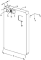
- the projection device 10' of the prior art three-dimensional imaging device when the projection device 10' of the prior art three-dimensional imaging device is mounted in an electronic mobile device 40' such as a mobile phone, The light source 11', the grating 12', the set of lenses 13' and the exit lens 14' are arranged linearly, and the thickness T' thereof increases the thickness t' of the handset. That is to say, according to say, according to the structure of the projection device 10' of the conventional three-dimensional imaging device, it can only be arranged along the thickness t' direction of the mobile phone, thereby increasing the thickness t' of the mobile phone, such that the projection device of the three-dimensional imaging device 10' is not suitable for installation in a thin and light mobile phone.
- the mobile phone for mounting such a three-dimensional imaging device as shown in Fig. 2 has a limited internal space, so that it is not easy to configure a heat dissipation mechanism for the light source 11'. That is to say, the projection device 10' of the conventional three-dimensional imaging device only increases the volume and thickness of the projection device 10' of the three-dimensional imaging device for the solution of its heat dissipation problem.
- the stereo image has broad application prospects, can simplify the measurement steps, save measurement time, and improve the precision and effect of the measurement, and further processing can also be used to derive a variety of new application methods.
- stereoscopic imaging devices are still limited by factors such as volume, and are often applied to separate devices, and are not suitable for use in electronic devices such as mobile phones, notebook computers, and tablet computers that are thin and light, thereby affecting Further popularization and application of three-dimensional imaging. Therefore, how to further reduce the thickness of the stereoscopic three-dimensional imaging device and overcome various problems arising from further reduction in thickness and thinning has become a problem to be solved by the present invention.
- An object of the present invention is to provide a light-converting three-dimensional imaging apparatus and projection apparatus and an application thereof, wherein the projection apparatus reduces a projection path of light emitted from a light source by providing a light steering element to reduce the projection apparatus Thickness and easy to install.
- An object of the present invention is to provide a light-converting three-dimensional imaging apparatus and a projection apparatus and an application thereof, which are suitable for installation in a mobile phone, a notebook computer, and a tablet electronic device such as a tablet computer which are intended to be thin and light, because the thickness of the projection device is effectively reduced.
- Electronic mobile devices are provided.
- An object of the present invention is to provide a light-converting three-dimensional imaging apparatus and projection apparatus and an application thereof, because the position of the grating element and the light source is moved relative to the central axis, thereby causing different distribution of the field of view of the projection pattern, and the projection light field can be achieved. Maximize the area of coincidence with the distribution of the light field, maximize the effective use of area, and save power.
- An object of the present invention is to provide a light-converting three-dimensional imaging apparatus and a projection apparatus and an application thereof, because the angles of the light-converting elements are different, thereby causing different distributions of the field of view of the projection pattern, and the projection light field and the shooting light can also be achieved. Maximize the field distribution coincidence area, maximize the effective use area, and save work Consumption.
- An object of the present invention is to provide a light-converting three-dimensional imaging apparatus and projection apparatus and an application thereof, wherein light emitted from the light source passes through a grating and a collecting lens group, and then reaches the light steering element to generate a turn, and finally Projecting from the exit lens, such that the effective thickness of the projection device corresponds to the total thickness of the light turning element and the exit lens, thereby being compared with the light source, grating, and collecting lens superimposed by layers in the prior art.
- the thickness of the projection device determined by the set and the exit lens is significantly reduced.
- An object of the present invention is to provide a light-converting three-dimensional imaging apparatus and a projection apparatus and an application thereof, wherein the light-steering element and the ejection lens of the projection apparatus are disposed along a thickness direction of an electronic mobile device, and a light source, the grating and the lens group may be disposed along a length direction (height direction) or a width direction of the electronic mobile device, such that the projection device of the light-converting three-dimensional imaging device is more suitable for being mounted on thin and light electronic In mobile devices.
- the exit lens may not be linearly arranged with the concentrating lens group, the grating and the light source.
- the projection device of the present invention is not a regular linear shape formed by cumulative accumulation of layers, but has a turning portion, the thickness of the turning portion determines the thickness of the projection device, thereby making the light conversion The thickness of the projection device of the three-dimensional imaging device is effectively reduced.
- An object of the present invention is to provide a light-converting three-dimensional imaging apparatus and projection apparatus and an application thereof, wherein the projection apparatus can be provided more and more because the light source of the projection apparatus is not arranged along a thickness direction. In this way, the problem of heat generation of the projection light source of the projection device can be effectively solved.
- the projection device can be mounted on a metal chassis that facilitates heat dissipation and assists optical correction of deviations in wavelength drift caused by heat generation of the light source through a background processor.
- An object of the present invention is to provide a light-converting three-dimensional imaging apparatus and a projection apparatus and an application thereof, wherein each apparatus of the three-dimensional imaging apparatus includes the projection apparatus, and the thickness thereof is reduced to 6 mm or less, so that the whole can be integrally Installed inside the electronic mobile device.
- An object of the present invention is to provide a light-converting three-dimensional imaging device and a projection device and an application thereof, wherein the projection device and the receiving device of the light-converting three-dimensional imaging device are oriented in the same direction as the display device of the electronic mobile device or Reversed, thereby greatly enhancing the application range of the three-dimensional imaging device and Optimize the use of feelings.
- An object of the present invention is to provide a light-converting three-dimensional imaging apparatus and projection apparatus and an application thereof. It is an object of the present invention to provide a circuit board apparatus, a light-converting three-dimensional imaging apparatus and a projection apparatus, and an application thereof, Focusing is achieved by a cylindrical suspension between a lens and a lens holder, thereby improving the imaging quality of the projection device to ensure the yield of the product.
- An object of the present invention is to provide a three-dimensional imaging device and a projection device and a projection device thereof, and the assembly is performed by using a threaded fit between the lens and the lens holder. It enables the size of the projection device to be significantly reduced, which facilitates its assembly on mobile electronic devices that are thin and light, such as mobile phones, tablets, and the like.
- An object of the present invention is to provide a light-converting three-dimensional imaging apparatus and a projection apparatus and an application thereof, and the assembly manner between the lens and the lens holder can also solve the debris caused by the screw fitting, and rotate the lens and/or The problem of the torsion caused by the lens holder, thereby reducing the difficulty of packaging the lens and the lens holder.
- An object of the present invention is to provide a light-converting three-dimensional imaging apparatus and projection apparatus and an application thereof, which do not need to provide rotational power for driving the lens and/or the lens holder when encapsulating the lens and the lens holder, In this way, not only the package precision of the lens and the lens holder can be improved, but also the time required for the package can be reduced and the complexity of the package device can be reduced to improve the production efficiency.
- An object of the present invention is to provide a light-converting three-dimensional imaging apparatus and a projection apparatus and an application thereof, wherein the lens is provided with a plurality of at least three side walls on a package surface with respect to a package surface structure of an existing lens.
- the medium tank can ensure that a sufficient amount of the connecting medium is preset to ensure the reliability of the projection device formed after the packaging, and in the process of packaging, the liquid connection medium can be prevented from overflowing, thereby It is not affected by the overflow of the connecting medium that the projection device is aesthetically pleasing in subsequent installation operations and its appearance.
- An object of the present invention is to provide a three-dimensional image forming apparatus and a projection apparatus and an application thereof, and the design of the medium tank can also reduce the difficulty of performing the glue filling operation on the position to ensure the projection. The operation of the device continued and proceeded smoothly.
- An object of the present invention is to provide a light-converting three-dimensional imaging apparatus and projection apparatus and an application thereof, since the connection medium does not overflow from the position of the medium groove, so that the lens and the lens holder are completed. After the encapsulation, there is no need to provide an operation of manually removing the overflowing of the connecting medium, thereby reducing the number of processes and saving labor costs.
- An object of the present invention is to provide a light-converting three-dimensional imaging device and projection device and application thereof, In the process of focusing the lens and the lens holder, it is allowed to compensate for the tilt, offset, angular deviation and the like of the single member only by moving the relative position of the lens holder to ensure that after focusing is completed The yield of the projection device is maximized.
- An object of the present invention is to provide a light-converting three-dimensional imaging apparatus and projection apparatus and an application thereof, which can avoid repetition of the lens and the lens holder during adjustment of the lens and the lens holder Operation to improve packaging efficiency.
- An object of the present invention is to provide a three-dimensional imaging device and a projection device and a projection device thereof, and the test device adopts a method of snapping the lens holder instead of clamping the lens holder to ensure that the lens holder is clamped.
- the stability of the mirror mount during movement and adjustment ensures accuracy and yield.
- An object of the present invention is to provide a light-converting three-dimensional imaging apparatus and a projection apparatus and an application thereof, which can pre-fix the lens and the lens holder after focusing on the lens and the lens holder, and The glue filling operation is performed on the lens and the lens holder in the subsequent manner, so that the product yield after packaging can be achieved.
- the relative positions of the lens and the lens holder after completion of focusing and before filling are not changed to ensure the imaging quality of the projection device formed after packaging.
- An object of the present invention is to provide a light-converting three-dimensional imaging apparatus and a projection apparatus and an application thereof, which allow the lens and the lens holder to be assembled, cored, adjusted, tested, etc. at one time.
- the operation of the process, and the secondary clamping of the lens and the lens holder can be avoided as much as possible to control the error after packaging, thereby improving the product yield.
- such a manner can also reduce the phenomenon that the projection device performs the turning during the assembly process, thereby preventing the external pollutants from polluting the internal structure of the projection device.
- An object of the present invention is to provide a light-converting three-dimensional imaging device and a projection device and an application thereof, wherein the circuit board device includes a heat dissipating member through which internal heat of the circuit board device is conducted Externally, the operating temperature of the circuit board device is lowered.
- An object of the present invention is to provide a three-dimensional image forming apparatus and a projection apparatus and an application thereof, wherein the overall strength of the circuit board device is enhanced by the reinforcement of the heat dissipating member, and the high temperature deformation of the circuit board is effectively solved. It is a problem to improve the flatness of the circuit board device, in other words, the heat sink helps the circuit board device to dissipate heat while maintaining its flatness.
- An object of the present invention is to provide a light-converting three-dimensional imaging device and a projection device and an application thereof, wherein the heat dissipating member can dissipate heat generated by the chip member in time, and the medium through the heat dissipating member is efficiently exported to the outside. Reducing the temperature of the chip component is suitable for efficient heat dissipation of the projection device.
- An object of the present invention is to provide a light-converting three-dimensional imaging device and a projection device and an application thereof, wherein the circuit board device includes a circuit board body, and the circuit board body provides a chip member and the heat dissipation member
- the docking space enables the chip component to transfer heat of the heat generating region to the heat dissipating member, thereby facilitating efficient derivation of heat generated by the projection light source, and is suitable for solving the heat dissipation problem in the structured light technology.
- An object of the present invention is to provide a light-converting three-dimensional imaging apparatus and projection apparatus and an application thereof, which can weld the chip component and the heat sink by the good thermal conductivity of the solder material, thereby preventing the use of D/A glue to cause internal temperature. Too high to help speed up the conduction between the chip component and the heat sink.
- An object of the present invention is to provide a light-converting three-dimensional imaging device and a projection device and an application thereof, wherein the soldering method uses a symmetrical pad design to reduce the uncontrollability of solder material over-reflow soldering, thereby facilitating To reduce the offset of the chip component when attached.
- An object of the present invention is to provide a three-dimensional optical imaging device and a projection device and an application thereof, wherein the conductive layer is directly turned on by the conductive layer and the pad line in the circuit board device, thereby effectively avoiding the use of conductive adhesive
- the impedance caused by the connection pads is large.
- An object of the present invention is to provide a light-converting three-dimensional imaging apparatus and projection apparatus and an application thereof, in which complicated mechanical manufacturing steps and devices are not required, and no major changes are made to the original structure of the circuit board, and related manufacturing costs are reduced. .
- An object of the present invention is to provide a light-converting three-dimensional imaging apparatus and projection apparatus and an application thereof, which provide an operating current of a VCSEL laser driving circuit through an energy storage unit.
- An object of the present invention is to provide a light-converting three-dimensional imaging apparatus and projection apparatus and an application thereof, which control circuit power supply processing module and VCSEL laser driving circuit and circuit of an energy storage unit through a switching circuit.
- An object of the present invention is to provide a light-converting three-dimensional imaging apparatus and a projection apparatus and an application thereof, the switching circuit comprising a field effect transistor for controlling on-off of the super capacitor and the power processing module and the VCSEL laser driving circuit.
- An object of the present invention is to provide a three-dimensional imaging device and a projection device and a projection device thereof, which are driven by a conventional DC drive to be pulse-driven, so that the heat generation of the VCSEL array is reduced, thereby working. More stable and more reliable.
- An object of the present invention is to provide a light-converting three-dimensional imaging apparatus and projection apparatus and an application thereof, which output PWM pulses such that the driving mode is changed from the original DC driving to the pulse driving.
- An object of the present invention is to provide a light-converting three-dimensional imaging apparatus and projection apparatus and an application thereof, which have a reduced drive circuit and a light weight of a product.
- An object of the present invention is to provide a three-dimensional imaging device and a projection device and a projection device thereof, which use a pulse gap to rapidly charge a large-capacity supercapacitor, and utilize a rapid discharge and a high energy density characteristic of a supercapacitor during a pulse width time. It solves the constant current and large current drive during the millisecond pulse.
- An object of the present invention is to provide a three-dimensional imaging device and a projection device and a projection device thereof, which provide a calibration method for a projection device, which is obtained by matching a camera module that has been calibrated to obtain a projection image. Calibration, greatly improving the decoding rate of the projected image.
- An object of the present invention is to provide a three-dimensional imaging device and a projection device and an application thereof, which use the internal parameters of the calibrated camera module to back-compensate the image to obtain an undistorted image, so as to conveniently obtain the calibration data of the projection device.
- a quantitative calibration of the projection device is achieved.
- An object of the present invention is to provide a three-dimensional imaging device and a projection device and a projection device thereof, and use the inverse compensation camera module to capture a projection image of the projection device, calculate internal and external parameters of the projection device, and realize calibration of the projection device. Solved the traditional problem of not being able to calibrate the projection device.
- An object of the present invention is to provide a light-converting three-dimensional imaging apparatus and a projection apparatus and an application thereof, which are simple in calibration method, high in efficiency, fast in calibration speed, and accurate in calibration data.
- An object of the present invention is to provide a three-dimensional optical imaging device and a projection device and an application thereof, which can objectively identify the detection result of the projection device by automatically detecting the projection image of the projection device, and increase the detection. Measuring accuracy and improving detection efficiency.
- An object of the present invention is to provide a three-dimensional optical imaging device and a projection device and an application thereof, which can automatically acquire the sharpness, the bad point, the quantitative calibration, and the decoded data of the projection device by using different detection softwares, and the operation is simple. Helps provide the test data required for the production process.
- An object of the present invention is to provide a three-dimensional imaging apparatus and a projection apparatus and a projection apparatus thereof, which acquire a projection image through a receiving apparatus, and then perform software analysis on the projection image by the processing apparatus, without visual inspection, thereby effectively reducing The damage of the human body greatly reduces the complexity of the detection operation.
- An object of the present invention is to provide a three-dimensional imaging device and a projection device and an application thereof, which objectively evaluate the performance of the projection device and process the image data of the projection device through a software algorithm, so that the detection result is more accurate and effectively reduces the directness through the naked eye. Distinguish the fatigue and avoid the false positive rate caused by subjective judgment.
- An object of the present invention is to provide a light-converting three-dimensional imaging apparatus and projection apparatus and an application thereof, which are suitable for evaluating projection apparatuses of different light source bands, breaking the limitation of using only visual inspection, and the receiving apparatus can recognize the corresponding projection apparatus The wavelength of the light source, thus, to distinguish the sharpness of the projected pattern of different bands.
- An object of the present invention is to provide a light-converting three-dimensional imaging device and a projection device and an application thereof, which can quickly detect a dead spot of a projection device without a microscope, thereby greatly reducing a dead point of the detection projection device by quickly acquiring a real-time projection pattern.
- the complexity is to provide a light-converting three-dimensional imaging device and a projection device and an application thereof, which can quickly detect a dead spot of a projection device without a microscope, thereby greatly reducing a dead point of the detection projection device by quickly acquiring a real-time projection pattern.
- An object of the present invention is to provide a three-dimensional imaging device and a projection device and an application thereof, which realize automatic calibration of the projection device, effectively improve the calibration efficiency of the projection device, expand the application range of the calibration data, and contribute to the optical image. Use of the field.
- An object of the present invention is to provide a light-converting three-dimensional imaging apparatus and a projection apparatus and an application thereof, which can obtain the actual projection angle and offset of the projection apparatus by comparing the actual projection image by software and comparing with the theoretical projection area. Objectively realize the quantitative calibration of the projection device, thereby providing an effective reference for subsequent projection correction.
- An object of the present invention is to provide a three-dimensional optical imaging device and a projection device and an application thereof, which can realize projection and decoding of still images and dynamic images by using automatic decoding software, thereby processing projection images based on still pictures or dynamic videos. , with greater flexibility and applicability.
- An object of the present invention is to provide a three-dimensional three-dimensional imaging apparatus and projection apparatus and an application thereof, which can make the projection code points easier to extract by preprocessing the projected image, and greatly improve the decoding rate of the projected image.
- An object of the present invention is to provide a three-dimensional optical imaging device and a projection device and an application thereof, which can extract code point information in an image and convert it into decoded data by using a decoding algorithm, so that the obtained decoded data is more accurate and beneficial.
- the development of subsequent applications expands the application range of the decoding algorithm.
- the present invention provides a light-converting projection apparatus for generating projection light in a three-dimensional imaging apparatus, comprising:
- a grating for modulating amplitude and/or phase of the projected light
- a light steering element for steering the projected light, wherein the projected light emitted by the light source passes through the exit lens from the light-emitting projection device after a steering action of the light-steering element The side is projected to the outside of the light-emitting projection device.
- the light turning element is disposed between the light collecting lens group and the light path of the emitting lens, so that the light emitted by the light source After passing through the grating and being refracted and concentrated by the collecting lens group, the light redirecting element is reached, and then the steering effect of the light turning element is performed, and finally the light-emitting projection device is emitted from the emitting lens.
- the light-steering element has a reflecting surface, and at least a portion of the projected light that reaches the light-steering element is reflected and emitted from the emitting lens
- the light projection device is described.
- the light steering element includes a refractive lens, and at least a portion of the projection light reaching the light deflection element is refracted and emitted from the emission lens
- the light projection device is described.
- the light steering element includes a refractive lens, and at least a portion of the projection light reaching the light deflection element is refracted and emitted from the emission lens
- the light projection device is described.
- the refractive lens is a triangular prism.
- the light steering element The reflecting surface is disposed obliquely with respect to a projection direction of the light source.
- the refractive lens of the light turning element is disposed obliquely with respect to a projection direction of the light source.
- the condensing lens group includes one or more lenses selected from one or more of a glass lens and a plastic lens.
- the thickness of the light conversion projection device is 6 mm or less.
- the light source is further provided with at least one heat dissipating component.
- the invention also provides a light-converting three-dimensional imaging device, comprising:
- At least one projection device comprising a light source, a grating, a collecting lens group, and a light
- the projection light emitted by the light source passes through the grating, the convergence of the condenser lens group, and the steering of the light steering element, through the emission a lens exiting the projection device from a side of the projection device;
- At least one receiving device At least one receiving device
- the receiving device receives the projected light reflected by the surface of the target object, and then transmits the information of the projected light to the processor, and the processor processes the information to obtain three-dimensional image information.
- the three-dimensional imaging device in the three-dimensional imaging device, at least a portion of the projected light reaching the light redirecting element is reflected and/or refracted to emit the projection device from the exit lens.
- the light turning element is disposed obliquely with respect to a projection direction of the light source.
- the light-converting three-dimensional imaging device comprises two or more of the projection devices arranged at a distance from each other.
- the light-converting three-dimensional imaging device is mounted in an electronic mobile device having a display screen, the projection device and the receiving device being located on the front or the back of the electronic mobile device, A display screen is used to display the three-dimensional image information.
- the invention also provides a light conversion projection device, the light conversion projection device being mounted on an electronic mobile device
- the light-projecting projection device includes:
- a light source disposed at one end of the light conversion projection device along a longitudinal direction; and at the turn
- the light source generates the projected light projected in a longitudinal direction, after at least a portion of the projection by the steering of the light turning element Light is emitted from the exit lens in a lateral direction.
- the light redirecting element is for reflecting and/or refracting the projected light.
- the light-projecting projection device further includes a grating, and a collecting lens group, wherein the projection light emitted by the light source is modulated by the grating in a longitudinal direction.
- the converging action of the concentrating lens group is then, after the steering of the light redirecting element, finally projecting the projection device from the exit lens in a lateral direction.
- the electronic mobile device is selected from the group consisting of a mobile phone, a notebook computer, and a tablet electronic device.
- the present invention also provides a method of mounting at least one light-projecting device inside an electronic mobile device for generating projected light in a three-dimensional imaging operation, the method comprising the steps of:
- the method further includes the steps of: setting the light source along the length direction of the electronic mobile device, the grating, the collecting lens group and the Light steering element.
- the method further comprises the steps of: setting the light source along the width direction of the electronic mobile device, the grating, the collecting lens group and the Light steering element.
- the light redirecting element is used for reflection and/or At least a portion of the projected light that reaches the light turning element is refracted.
- the electronic mobile device is selected from the group consisting of a mobile phone, a notebook computer, and a tablet electronic device.
- the present invention also provides a method of generating projection light of a projection device of a three-dimensional imaging device, the method comprising the following steps:
- the light emitted by the light source passes through a grating to modulate the amplitude and/or phase of the light;
- the deflected light is emitted from the side of the projection device through an exit lens to produce the projected light.
- the step (d) comprises the step of reflecting at least a portion of the light refracted from the concentrating lens group by the light turning element.
- the step (d) includes the step of refracting at least a portion of the light refracted from the concentrating lens group by the light turning element.
- the invention also provides an imaging method of a three-dimensional imaging device, comprising the following steps:
- (G) receiving means receiving the projected light reflected by the surface of the target object and acquiring parameter information
- the processor processes the parameter information to obtain a three-dimensional image.
- the light reaching the light redirecting element is reflected and/or refracted and exits the projection device from the exit lens.
- the light source emits light toward the front side, and after the steering of the light steering element, the projection device is emitted from the left or right side of the projection device. .
- the light source emits light toward the front side, and after the steering of the light steering element, the projection device is emitted from the upper side or the lower side of the projection device.
- a light conversion projection apparatus for generating projection light in a three-dimensional imaging apparatus, comprising:
- a light generator for emitting the projected light
- a light turning element for steering the projected light, wherein the projected light emitted by the light generator passes through the exit lens from the light after the steering of the light redirecting element
- the side of the projection device is projected to the outside of the light-converting projection device.
- the light turning element is disposed between the light collecting lens group and the light path of the emitting lens, so that the light emitted by the light generator Light passes through the optical encoder to become coded light, and is refracted and concentrated by the concentrating lens group, reaches the light steering element, and then passes through the steering effect of the light steering element, and finally exits from the exit lens.
- the light conversion projection device in the light conversion projection device, the light turning element is disposed between the light collecting lens group and the light path of the emitting lens, so that the light emitted by the light generator Light passes through the optical encoder to become coded light, and is refracted and concentrated by the concentrating lens group, reaches the light steering element, and then passes through the steering effect of the light steering element, and finally exits from the exit lens.
- the projection device in the above-described light-converting projection device, at least a portion of the projection light reaching the light-steering element is reflected and/or refracted, and the projection device is emitted from the emission lens.
- the light turning element is disposed obliquely with respect to a projection direction of the light generator.
- the light turning element is a triangular prism.
- the thickness of the light conversion projection device is 6 mm or less.
- the present invention also provides a projection apparatus comprising:
- the lens includes a housing, and the housing is provided with a mounting cavity;
- the lens holder including a lens holder housing, the lens holder housing being provided with a mounting end, wherein the mounting end portion extends to the mounting cavity to be in the housing and the housing A focusing gap is formed between the mirror housings for subsequent focusing.
- the housing is further provided with at least one medium slot for accommodating a connecting medium, and each of the medium slots is located between the housing and the mirror housing.
- each of the media slots has at least three side walls.
- each of the media slots is located at a corner of the housing.
- the plane of the end of each of the media slots is coplanar with the plane in which the ends of the housing are located.
- the mounting cavity is a cylindrical cavity
- the mounting end is cylindrical
- the inner diameter of the mounting cavity is larger than the outer diameter of the mounting end.
- the mirror housing is further provided with a symmetrical positioning element.
- the present invention also provides a testing device for a screwless module, comprising:
- a lens fixing member for fixing a lens for fixing a lens
- a lens holder fixing member for fixing a lens holder; wherein the lens holder fixing member is configured to move relative to the lens fixing member;
- a light source for exposing the lens that completes the focusing to the mounting surface of the lens holder to solidify a connection medium disposed on the mounting surface of the lens and the lens holder.
- the testing device further includes a base, the lens fixing member, the lens holder fixing member and the point light source are respectively disposed with the base, and the point light source is located at the Between the lens fixing member and the mirror holder fixing member.
- the lens fixing member comprises:
- a lens fixing block disposed on the first adjustment platform, and the lens fixing block is synchronized with movement of the first adjustment platform, wherein the lens fixing block is configured to fix the lens;
- the lens holder fixing member comprises:
- a lens holder fixing block disposed on the second adjustment platform, and the mirror holder fixing block and the first 2. Adjusting the motion synchronization of the platform, wherein the lens holder fixing block is used to fix the lens holder.
- the second adjustment platform is linearly movably disposed on the guide rail.
- the lens fixing member further includes an adjusting member disposed between the first adjusting platform and the lens fixing block.
- the testing device further comprises at least one clamping element respectively disposed on the base for clamping the lens and/or the lens holder.
- the clamping element comprises a first clamping arm and a second clamping arm, and a clamping cavity is formed between the first clamping arm and the second clamping arm
- the first clamping arm is provided with a card slot, and the card slot faces the clamping cavity.
- the lens holder fixing member is further provided with at least one probe.
- the present invention also provides a focusing method of a projection device, wherein the method comprises the steps of:
- a mounting cavity is formed in a housing of the lens, and a mounting end is formed on a mirror housing of the lens mount to extend the mounting end To the mounting cavity to form the focusing gap between the housing and the mirror housing.
- the mounting cavity is a cylindrical cavity
- the mounting end is cylindrical
- the inner diameter of the mounting cavity is larger than the outer diameter of the mounting end.
- the present invention also provides a method of packaging a screwless module, wherein the method comprises the steps of:
- the method further comprises the step of: (IV) adding The unthreaded module is heated to enhance the assembly strength of the lens and the lens holder.
- a mounting cavity is formed in a housing of the lens, and a mounting end is formed on a mirror housing of the lens mount to extend the mounting end To the mounting cavity to form a focusing gap between the housing and the mirror housing for focusing.
- At least one medium groove is formed on a mounting surface of the housing for accommodating the connection medium, and each of the medium grooves is located in the housing and the housing Between the mirror housings.
- the mounting cavity is a cylindrical cavity
- the mounting end is cylindrical
- the inner diameter of the mounting cavity is larger than the outer diameter of the mounting end.
- each of the media slots has at least three side walls.
- the plane of the end of each of the media slots is coplanar with the plane in which the ends of the housing are located.
- each of the media slots is located at a corner of the housing.
- the connecting medium is a UV glue.
- the present invention also provides a method for designing a screwless module, wherein the screwless module includes a lens and a lens holder, the lens includes a housing, and the lens holder includes a mirror mount housing, wherein the method includes forming a focus gap between the housing of the kit and the mirror mount housing, and between the housing and the mirror mount housing after assembly The inclination can be adjusted.
- At least one medium groove is formed at an end of the casing for accommodating a connection medium, wherein the connection medium is pre-fixed after curing And the mirror base.
- a mounting cavity is formed in the housing to form a mounting end to the mirror housing, wherein the mounting end extends to the mounting cavity, And the mounting cavity is a cylindrical cavity, the mounting end is a cylindrical structure, and the inner diameter of the mounting cavity is larger than the outer diameter of the mounting end.
- each of the media slots has at least three side walls.
- the present invention also provides a heat dissipating circuit board device comprising:
- circuit board body the circuit board body is provided with a heat dissipation cavity
- a heat dissipating member one end of the heat dissipating member extends into the heat dissipating cavity to be connected to the chip component, thereby conducting heat for conducting the chip component to the outside.
- the heat sink includes a guiding portion and an extension portion extending integrally from the extension portion toward the chip member for abutting the chip member,
- the extension portion is attached to the circuit board main body.
- the heat dissipating circuit board device further includes at least one attaching layer, the attaching layer being respectively disposed between the chip component, the heat sink, and the circuit board main body for fitting The chip component, the heat sink, and the circuit board body.
- the diameter of the heat sink guiding portion is matched to the inner diameter of the heat dissipation cavity of the circuit board body for the guiding portion to be butted to the chip component through the heat dissipation cavity.
- an extension portion of the heat dissipating member is overlapped with a base of the circuit board main body for enlarging a heat dissipating area of the heat dissipating member and reinforcing a base of the circuit board main body, wherein The heat dissipation cavity is formed on the base.
- the attaching layer includes a first attaching layer and a second attaching layer, and the first attaching layer is disposed on the guiding portion of the chip member and the heat sink
- the second attaching layer is disposed between the extension of the heat sink and the base of the circuit board body for The heat sink and the circuit board body are attached.
- the first attaching layer is a solder layer that is thermally conductively butted to the chip member and the heat sink.
- the heat sink further includes at least one protrusion.
- the base of the circuit board body is provided with at least one through hole, and the protrusion is from the extension of the heat sink The through hole of the base extends for engaging the heat sink and the base of the circuit board body such that an extension of the heat sink is attached to the circuit board body.
- the chip component in the first attaching layer, is symmetrically butted to the pedestal of the circuit board main body and the heat dissipating member for reducing the soldering bias of the chip component shift.
- the chip component in the first attaching layer, is symmetrically butted to the pedestal of the circuit board main body and the heat dissipating member for reducing the soldering bias of the chip component shift.
- the heat sink is provided with a slot, and the slot shape is symmetrically formed on the guiding portion of the heat sink for guiding the chip member to symmetrically solder the heat sink unit.
- the heat sink is a heat dissipating steel sheet.
- the heat sinkable circuit board device is a circuit board device of the projection device.
- the present invention also provides a heat dissipation method of a heat dissipating circuit board device, wherein the heat dissipation method includes the steps of: setting a heat of a chip component of a circuit board main body connected to the circuit board device through A heat sink of the base heat dissipation cavity is conducted to the outside thereof.
- the heat dissipation method further includes a step of: conducting heat generated by the chip component to a guiding portion of the heat sink through a first attaching layer, wherein the first attaching layer is A thermally conductive solder layer.
- the heat dissipation method further comprises the steps of:
- Heat is radiated radially outward from the extension to the outside for expansion of the area.
- the heat dissipation method further includes the step of: transmitting heat generated by the chip component to the circuit board body through the first attaching layer, wherein the circuit board body is thermally conductive Flexible circuit board.
- the heat dissipation method further includes the step of: bonding the heat sink to the base of the circuit board body through a protrusion provided in the through hole pad of the circuit board body, The extension portion of the heat sink is attached to the circuit board main body.
- the present invention also provides a method of manufacturing a heat dissipating circuit board device, wherein the manufacturing method comprises the steps of:
- the manufacturing method further includes the step (q) of bonding the circuit board main body, the chip member, and the heat sink by at least one attaching layer.
- the manufacturing method further includes the step (r) of electrically conducting the chip member and the heat sink and/or the board body.
- the step (q) comprises the steps of:
- the step (p) comprises the step (p.1) of symmetrically docking the chip component to the heat sink for reducing the offset caused by the docking of the chip component.
- said step (p.1) comprises the steps of:
- the step (p.1) further comprises the step of:
- said step (q.2) comprises the steps of:
- the present invention also provides a USB powered pulsed VCSEL laser driving circuit, comprising:
- a VCSEL laser driving circuit for driving a VCSEL laser
- a storage protection circuit for storing electrical energy, providing the VCSEL laser driving circuit to drive electrical energy, the energy storage protection circuit electrically connected to the VCSEL laser driving circuit;
- a microprocessor unit for controlling the energy storage protection circuit and the VCSEL laser drive circuit
- a power module for providing power to the energy storage protection unit and the microprocessor unit, wherein the power module includes a USB interface and a power processing module, and the power processing module is electrically connected to the USB interface .
- the energy storage protection circuit includes an energy storage unit, and the power processing module is to the energy storage unit when the VCSEL laser driving circuit outputs a pulse at a low level. Charging.
- the power processing module is electrically connected to the energy storage unit.
- the power processing module is electrically connected to the microprocessor unit.
- the energy storage unit supplies electrical energy to the VCSEL laser drive circuit when the VCSEL laser drive circuit outputs a high level.
- the energy storage protection circuit includes a switching circuit that controls the circuit of the power processing module and the VCSEL laser driving circuit and the energy storage unit to be turned on and off.
- the energy storage unit comprises at least one supercapacitor.
- the switching circuit comprises a field effect transistor.
- the FET controls the on and off of the VCSEL laser driving circuit and the power module and the super capacitor.
- the VCSEL laser driving circuit includes a DC/DC conversion power supply module and a sampling feedback module, and the DC/DC conversion power supply module is configured to convert the energy storage unit input power, the sampling A feedback module is used to feed back information to the microprocessor unit.
- the VCSEL laser drive circuit drives the VCSEL laser with a PWM pulse.
- the VCSEL laser drive circuit drives the VCSEL laser with a dual PWM pulse.
- the USB powered pulsed VCSEL laser driver circuit further includes a UART programming interface coupled to the microprocessor unit.
- the present invention also provides a VCSEL laser driving method, comprising the steps of:
- the VCSEL laser drive circuit pulses the VCSEL laser.
- the method is applicable to a USB power supply mode.
- the power module in the step ( ⁇ ), includes a USB An interface and a power processing module, the power processing module being electrically coupled to the USB interface.
- the energy storage protection circuit includes an energy storage unit and a switch circuit, and the switch circuit controls communication between the energy storage unit and the power processing module.
- the VCSEL laser drive circuit uses a pulse to drive the VCSEL laser.
- the power processing module charges the energy storage unit, and when the VCSEL laser driving circuit outputs a high level, An energy storage unit provides electrical energy to the VCSEL laser drive circuit.
- the energy storage unit comprises at least one supercapacitor.
- the switching circuit comprises a field effect transistor.
- the field effect transistor controls on and off of the VCSEL laser driving circuit and the power module and the super capacitor.
- the VCSEL laser drive circuit drives the VCSEL array with PWM pulses.
- the VCSEL laser drive circuit drives the VCSEL array with dual PWM pulses.
- the VCSEL laser driving method further comprises the step of modifying the PWM pulse pulse width duty cycle through a UART programming interface.
- the present invention also provides a calibration method of a projection device, wherein the calibration method comprises the following steps:
- an internal parameter and an external parameter of the camera module are acquired, and the camera module is inversely compensated to obtain an undistorted image.
- the camera module is calibrated by a conventional calibration method, an automatic visual calibration method, or a self-calibration method.
- step (z) according to the calibration mode of the camera module Calculate the internal and external parameters of the projection device.
- the internal and external parameters of the projection device are calculated according to the calibration mode of the camera module.
- the internal and external parameters of the projection device are calculated according to the calibration mode of the camera module.
- a projection structured light system for detecting a projection device comprising the steps of:
- the detecting method further comprises the step of (S400): saving data of the projection device for providing an objective reference to the projection device.
- the detecting method further comprises the step of (S500) establishing a standard relative position model of the receiving device and the projection device for acquiring the projected image.
- the step (S100) comprises the step (S101) of projecting a projection mask of the projection device to the projection target to form the projection image.
- the step (S300) includes a step (S310): calculating, by the detection software, the projection image resolution force for automatically acquiring the pattern definition of the projection mask of the projection device .
- said step (S200) comprises the step (S210): the projected image on said projection target is received by said receiving means by diffuse reflection.
- the receiving device in said step (S200) is a light-sensitive camera for correspondingly identifying the wavelength of the light source projected by said projection device.
- the step (S500) comprises the step (S510): the photosensitive camera and the projection device establish a standard relative position model by modeling, such that the field of view coverage of the receiving device Greater than the projection surface of the projection device.
- the step (S300) comprises a step (S320) of detecting the projected image by the detection software for automatically acquiring a dead-end detection result of the projection device.
- the step (S320) comprises the steps of:
- the detection area is a block area of m*n size, and when the block area is different from the code point of the projection mask, it is automatically determined.
- the block area is a dead point.
- the projection image is acquired by the receiving device in the step (S200) for performing fast real-time dead pixel detection on the projection image.
- the step (S300) comprises the step of (S330) detecting the projected image by the detection software for automatically acquiring the quantized calibration data of the projection device.
- the step (S330) comprises the steps of:
- said step (S331) comprises the step (S3311) of obtaining a theoretical projection range by the structure and distance of said projection means.
- the step (S332) comprises the steps of:
- the step (S333) comprises the steps of:
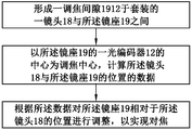
- the actual throwing angle y1' of the projection device is used as calibration data for adjusting the projection angle of the projection device by the reverse bias value such that the projected image is corrected to the theoretical projection region.
- the step (S400) includes the step (S430) of transmitting the calibration data to the compensation software of the finished module for objectively providing a reference for the late software compensation data of the finished module.
- the step (S300) comprises a step (S340) of detecting the projected image by the detection software for automatically acquiring decoded data of the projected image.
- the step (S340) comprises the steps of:
- the step (S341) comprises the steps of:
- the decoding algorithm of the step (S343) comprises the steps of:
- the decoding window in step (S343) is a window of 2*3 size.
- the decoding constructs the symbol using an m-sequence pseudo-random sequence such that the position of the decoded data corresponding to each 2*3 decoding window in the sequence of projection mask patterns is uniquely determined. It is suitable for dynamic decoding and static decoding, wherein the m-sequence pseudo-random sequence is a 6-sequence pseudo-random sequence.
- the decoding algorithm of (S343) further includes a step (S3434) of defining a symbol type as 0+, 0-, 1+, 1-, and simultaneously returning 0+ and 1+
- the class is c, which classifies 0- and 1- as b for converting the projected image model into a decoded sequence.
- FIG. 1 is a schematic cross-sectional view of a projection device of a three-dimensional imaging device according to the prior art.
- FIG. 2 is a schematic structural view of a projection device according to the above-described prior art three-dimensional imaging device mounted on a mobile phone.
- 3A is a cross-sectional structural view of a projection device of a three-dimensional imaging device in accordance with a preferred embodiment of the present invention.
- 3B is a cross-sectional structural view of a projection apparatus of a three-dimensional imaging apparatus according to a modified embodiment of the above preferred embodiment of the present invention.
- FIG. 4 is a schematic view showing the operation of a three-dimensional imaging apparatus according to the above preferred embodiment of the present invention.
- Figure 5 is a schematic illustration of the operation of a plurality of projection devices of a three-dimensional imaging device in accordance with the above-described preferred embodiment of the present invention.
- Fig. 6 is a schematic view showing a mounting manner of a projection apparatus of a three-dimensional imaging apparatus according to the above preferred embodiment of the present invention mounted on an electronic device.
- Figure 7 is a schematic view showing another mounting manner of the projection device of the three-dimensional imaging device mounted on the electronic device according to the above preferred embodiment of the present invention.
- Figure 8 is a flow chart showing a method of generating projection light by a projection device of a three-dimensional imaging device according to the above preferred embodiment of the present invention.
- FIG. 9 is a flow chart showing a method of performing three-dimensional imaging using a three-dimensional imaging apparatus according to the above-described preferred embodiment of the present invention.
- FIGS. 10A and 10B are perspective views, respectively, of a lens of a projection device in accordance with a preferred embodiment of the present invention.
- FIG. 11A and 11B are respectively perspective views of a lens holder of a projection apparatus according to the above preferred embodiment of the present invention.
- Figure 12 is a perspective view of a projection apparatus in accordance with the above preferred embodiment of the present invention.
- Figure 13 is a cross-sectional view taken along line A-A of Figure 10A.
- Figure 14 is a cross-sectional view taken along line B-B of Figure 12;
- Figure 15 is a partially enlarged schematic view of Figure 14 at the S position.
- Figure 16 is a schematic illustration of the relationship between the mounting cavity and the mounting end in accordance with the above-described preferred embodiment of the present invention.
- Figure 17 is a perspective schematic view of a test apparatus in accordance with a preferred embodiment of the present invention.
- Figure 18 is a partial schematic view of a lens fixing member according to the above preferred embodiment of the present invention.
- Figure 19 is a partial schematic view of a lens holder fixing member according to the above preferred embodiment of the present invention.
- Figure 20 is a partial schematic view of a test apparatus in accordance with the above-described preferred embodiment of the present invention.
- Figure 21 is a flow chart showing the operation of the test apparatus according to the above preferred embodiment of the present invention.
- 22A and 22B are respectively schematic views of a focusing process in accordance with the above-described preferred embodiment of the present invention.
- 23A and 23B are respectively schematic views showing an assembly process of a lens and a lens holder according to the above preferred embodiment of the present invention.
- Figure 24 is a schematic illustration of a focusing process in accordance with the present invention.
- Figure 25 is a flow chart showing the packaging of the screwless module of the three-dimensional image forming apparatus according to the present invention.
- Figure 26 is an exploded view of a structure in accordance with a preferred embodiment of the present invention.
- Figure 27 is a schematic view showing the structure of the above preferred embodiment in accordance with the present invention.
- Figure 28A is a cross-sectional view in the direction of Figure 27A-A', in accordance with the above-described preferred embodiment of the present invention.
- Figure 28B is a schematic view of heat dissipation in accordance with the above-described preferred embodiment of the present invention.
- Figure 29 is an exploded perspective view showing a first modification of the above preferred embodiment of the present invention.
- Figure 30A is a cross-sectional view showing the structure of a first modification of the above preferred embodiment of the present invention.
- Figure 30B is a schematic view of a heat dissipation according to a first variation of the above preferred embodiment of the present invention.
- Figure 31 is an exploded perspective view showing a second modification of the above preferred embodiment of the present invention.
- Figure 32 is a schematic view showing the structure of a second modification of the above preferred embodiment of the present invention.
- Figure 33A is a cross-sectional view in the direction of Figure 32B-B' in accordance with a second modification of the above-described preferred embodiment of the present invention.
- Figure 33B is a schematic view of a heat dissipation according to a second variation of the above preferred embodiment of the present invention.
- Figure 34 is a circuit block diagram of a USB powered pulsed VCSEL laser driver circuit in accordance with a preferred embodiment of the present invention.
- 35 is a USB powered pulsed VCSEL laser driver in accordance with a preferred embodiment of the present invention. Another circuit block diagram of the moving circuit.
- 36 is a schematic diagram of energy storage of a USB powered pulsed VCSEL laser drive circuit in accordance with a preferred embodiment of the present invention.
- FIG. 37 is a schematic diagram of the driving of a USB powered pulsed VCSEL laser driver circuit in accordance with a preferred embodiment of the present invention.
- FIG. 38 is a circuit diagram of a USB powered pulsed VCSEL laser driver circuit in accordance with a preferred embodiment of the present invention.
- 39 is a further circuit block diagram of a USB powered pulsed VCSEL laser driver circuit in accordance with a preferred embodiment of the present invention.
- FIG. 40 is a block diagram of a method of a USB powered pulsed VCSEL laser driver circuit in accordance with a preferred embodiment of the present invention.
- Figure 41 is a flow chart for calibrating a projection device in accordance with a preferred embodiment of the present invention.
- 42A and 42B are respectively schematic diagrams of image compensation before and after image capture by a camera module according to a preferred embodiment of the present invention.
- Figure 43 is a schematic illustration of a block in accordance with a preferred embodiment of the present invention.
- Figure 44 is a schematic view showing the structure of the above preferred embodiment in accordance with the present invention.
- Figure 45A is a block diagram showing the calibration of the above-described preferred embodiment of the present invention.
- Figure 45B is a schematic illustration of the position of a calibration detection anchor point in accordance with the above-described preferred embodiment of the present invention.
- Figure 46A is a projection mask diagram of the above described preferred embodiment in accordance with the present invention.
- Figure 46B is a schematic illustration of a mask window in accordance with the above-described preferred embodiment of the present invention.
- Figure 47A is an original projected image in accordance with the above-described preferred embodiment of the present invention.
- Figure 47B is a pre-processed image in accordance with the above-described preferred embodiment of the present invention.
- Figure 47C is a symbol type image in accordance with the above-described preferred embodiment of the present invention.
- Figure 48 is a flow diagram showing the above preferred embodiment of the present invention.
- Figure 49 is a flow chart showing the calibration detection process in accordance with the above preferred embodiment of the present invention.
- Figure 50 is a flow chart showing the decoding detection process in accordance with the above preferred embodiment of the present invention.
- 3A to 7 are schematic views showing the structure of a light-converting three-dimensional imaging apparatus and a projection apparatus thereof according to a preferred embodiment of the present invention.
- the light-converting three-dimensional imaging device is adapted to be mounted on an electronic mobile device 40, the light-converting three-dimensional imaging device comprising at least one of the projection device 10, at least one receiving device 20, and a processor 30, wherein The receiving device 20 is coupled to the processor 30.
- the projection device 10 emits projection light to the surface of the target object, is then reflected, and then receives the acquisition by the receiving device 20, and the receiving device 20 transmits the collected information to the processor 30 for processing, thereby obtaining the The information of the target object to realize three-dimensional stereo imaging, and further realize deep expansion functions such as measurement and drawing.
- the projection device 10 of the three-dimensional imaging device includes a light generator, which can be implemented as a light source 11, an optical encoder 12, a concentrating lens group 13, and an emission device.
- Lens 14 The light source 11 generates light, and the optical encoder 12 encodes the light generated by the light source 11.
- the optical encoder can be implemented as a grating 12, and the light generated by the light source 11 passes through The grating 12 is then modulated in amplitude and/or phase to produce coded light for recognition, which is projected from the exit lens 14 to the outside by the converging action of the collecting lens group 13.
- the projection device 10 further includes a light redirecting element 15 that causes the light reaching the light turning element 15 to be turned and finally passes through the exit lens 14 from the projection device.
- the side of 10 is shot. That is, the light source 11, the grating 12, and the collecting lens group 13 are arranged along the one end of the projection device 10 toward the other end, and finally, the steering through the light steering element 15.
- the light generated by the light source 11 is not emitted from the other end surface of the projection device 10, but is emitted from the side surface of the projection device 10.
- the light source 11 may be a vertical cavity surface emitting laser, a laser diode, a light emitting diode, or the like, and the generated light may be visible light, infrared light, or ultraviolet light.
- the grating 12 has a grating pattern of a predetermined pattern and divides the light generated by the light source 11 into bundles of light.
- the concentrating lens group 13 includes one or more lenses, and each of the lenses may be various convex or concave lenses, such as the lenses 131, 132, 133, 134, 135, and 136 shown in FIG. 3A.
- each of the lenses 131, 132, 133, 134, 135, and 136 is refracted, and is concentrated, so that the condensing lens group 13 can function as a light concentrating by a combination of different lenses.
- the light generated by the projection device 10 is finally projected from the exit lens 14 onto the surface of the target object, and then reflected. Received by the receiving device 20.
- the projection device 10 of the present invention is further provided with a light redirecting element 15 to steer the projection path of the light in the projection device 10, ultimately Light can be emitted from the side of the projection device 10.
- the entire projection device 10 may not be disposed along the thickness direction of the electronic mobile device as shown in FIG. 2, but may be similar to the width direction or the length direction of the electronic mobile device 40 in FIGS. 6 and 7 ( The height direction is set so as to facilitate the mounting of the three-dimensional imaging apparatus of the present invention inside the thin and light electronic mobile device 40.
- the electronic mobile device 40 can be a mobile phone, a notebook computer, a tablet device such as a tablet computer, or the like.
- the light redirecting element 15 is disposed in a light path of the projection device 10 and is selectively positionable between the light source 11 and the light path of the grating 12, or the grating 12 and the collecting lens group 13 Between the light paths, or between the light collecting lens group 13 and the light path of the exit lens 14.
- the light redirecting element 15 diverts light passing through the collecting lens group 13 and then projects from the emitting lens 14 to the outside of the projection device 10. That is, in the example shown in FIG. 3A, the light steering element 15 is disposed between the light collecting lens group 13 and the light path of the emitting lens 14 to change the light from the collecting lens group 13. The direction in which the light is projected.
- the thickness T of the projection device 10 is primarily dependent on the total thickness of the light turning element 15 and the exit lens 14.
- the present invention is compared to the thickness T' of the conventional projection device determined by the accumulation of the light source 11', the grating 12', the set of lenses 13', and the layers of the exit lens 14'.
- the thickness T of the projection device 10 is significantly reduced.
- the light redirecting element 15 has a reflecting surface 151, and the light generated by the light source 11 sequentially passes through the grating 12 and the collecting lens group 13 to reach the light.
- the reflecting surface 151 of the steering element 15 is reflected and passed through the exit lens 14 to be projected to the outside of the projection device 10.
- the exit lens 14 can function to distribute the emitted light of the projection device 10 to distribute the emitted light of the projection device 10 to various directions as needed.
- the reflecting surface 151 may be a mirror surface that is disposed obliquely with respect to a projection direction of the light of the light source 11 so as to pass through the respective lenses 131, 132, 133, 134 of the collecting lens group 13 and The light of 135 reaches the light redirecting element 15 and is reflected by the reflecting surface 151, thereby generating a turn of the optical path, and then exiting from the exiting lens 14.
- the lenses 131-136 of the projection device 10 may be glass lenses, or a combination of a plastic lens and a glass lens, that is, a wave-molding lens, so as not to impair the light effect. On the basis of ensuring maximum cost-effectiveness. Additionally, the lenses 131-136 may employ miniaturized glass aspherical lenses to further reduce the volume of the projection device 10.
- the projection device 10 may further include a housing 16 for housing and mounting the light source 11, the grating 12, the collecting lens group 13, the exit lens 14 and the light redirecting element 15.
- the thickness T of the projection device 10 can be substantially equivalent to the diameter of the housing 16 of the projection device 10, and
- the thickness T' generated after the projection device 10' is mounted on the electronic mobile device 40' is equivalent to the length of the projection device 10'. Therefore, the structure of the present invention causes the thickness T of the projection device 10 to be remarkably reduced, and in the three-dimensional imaging device of the present invention, the least likely to reduce the thickness is the projection device thereof, which is provided by the present invention.
- the solution can effectively reduce the thickness T of the projection device 10, so that the three-dimensional imaging device of the present invention and the projection device 10 thereof can be integrally mounted inside the electronic mobile device 40 without increasing The thickness t of the electronic mobile device 40 is large.
- the light redirecting element 15 may include a refractive lens 152 through which light passing through the collecting lens group 13 reaches the refractive lens 152.
- the refractive lens 152 is refracted and then directed toward the exit lens 14, from which the projection device 10 is ejected.
- the light of the projection light source 11 is offset upward and downward by a distance perpendicular to the optical axis direction, so that the final projection direction is biased to the left/right direction, so that the position of the shooting module can be maximized.
- the use of the projected field of view That is to say, most of the light of the projection light source 11 can be collected by the imaging module.
- the light redirecting element 15 can change the projection direction of the light of the projection device 10 not only by the reflection effect, but also the projection direction of the light of the projection device 10 by the refraction action. It is to be understood that the light redirecting element 15 may also include a light reflecting member and a refractive member to both reflect and refract light from the collecting lens group 13.
- the refractive lens 152 may be implemented as a prism, such as a triangular prism, to function to refract light. It is worth mentioning that the prism may also be provided with a reflecting surface 151 disposed obliquely with respect to the projection direction of the light of the light source 11, so that the light passing through the collecting lens group 13 will be reflected by reflection and refraction. Make a turn.
- the light-steering element 15 in this embodiment may not be limited to the above structure in a specific application, as long as it is a device capable of reflection and/or refraction, and in the subsequent steps, After the receiving device 20 receives the optical signal and transmits it to the processor 30, the software can be used on the optical path. Change the offset to calibrate.
- the projection device 10 is configured with a heat dissipation structure.
- the light source 11 of the projection device 10 is provided with a heat dissipating component 17, which may be a metal frame, so that the heat generated by the light source 11 is effectively and timely transmitted and distributed to the electronic mobile device.
- the exterior of 40, and thus the present invention also solves the problem of heat dissipation of the projection device 10 of the three-dimensional imaging device.
- the processor 30 can correct the offset of the light caused by the setting of the light redirecting element 15, thereby ensuring the accuracy and authenticity of the final data.
- the processor 30 may also assist in optically correcting variations in wavelength drift or the like caused by heat generation of the light source 11.
- the projection device 10 of the present invention is disposed at the first end of the projection device 10 along the longitudinal direction (ie, along the X-axis direction in the drawing).
- the light source 11 and the opposite second end are provided with the light redirecting element 15 disposed along the lateral direction (ie, along the Y-axis direction in the drawing) such that the light of the projection device 10 is from the lateral direction.
- the side is ejected, rather than being projected in the longitudinal direction and then projecting the projection device 10 in the longitudinal direction.
- the direction in which the light generated by the light source 11 is projected is not the same longitudinal direction as the direction in which the exit lens 14 is finally emitted, but two directions which are substantially perpendicular to each other, that is, the longitudinal direction and the lateral direction. It can also be said that, as shown in FIG. 3A, when light is generated, the light redirecting element 15 projected from the first end to the second end along the length direction of the projection device 10 passes through the light steering After the steering of the element 15, it is emitted from the side of the projection device 10.
- one or more of the light emitting elements of the light source 11 can define an emitting surface 110 that defines an exit surface 140.
- the emitting surface 110 and the emitting surface 140 may be arranged in directions substantially perpendicular to each other.
- the emitting surface of the light source 11' can be arranged coaxially with the exit surface of the exit lens 14' and substantially parallel to each other.
- the components of the projection device 10' are stacked to make the thickness of the projection device 10' difficult to be less than 15 mm, and the thickness of the projection device 10 of the present invention may be 6mm or less.
- the thickness of the projection device 10 of the present invention may be 6mm or less.
- FIG. 6 when the light source 11, the grating 12, the collecting lens group 13, and the light redirecting element 15 of the projection device 10 are along the width direction of the electronic mobile device 40, In configuration, the total length of the grating 12, the collecting lens group 13 and the light redirecting element 15 is significantly smaller than the width w of the electronic mobile device 40, so that the electronic mobile device 40 is internally provided with sufficient The space accommodates the projection device 10.
- FIG. 6 when the light source 11, the grating 12, the collecting lens group 13, and the light redirecting element 15 of the projection device 10 are along the width direction of the electronic mobile device 40, In configuration, the total length of the grating 12, the collecting lens group 13 and the light redirecting element 15 is significantly smaller than the width w of the electronic mobile device 40
- the grating 12, the collecting lens group 13 and the light redirecting element 15 are along the electronic mobile device 40
- the total length of the grating 12, the collecting lens group 13 and the light redirecting element 15 is significantly smaller than the length h of the electronic mobile device 40, such that the electronic mobile device
- the interior 40 is also provided with sufficient space to accommodate the projection device 10.
- the projection device 10 and the receiving device 20 of the light-converting three-dimensional imaging device of the present invention may be located on the front or back of the electronic mobile device 40, and the orientation thereof is capable of interacting with the electronic mobile device 40.
- the display device such as the display screen, is oriented in the same direction or in the opposite direction, thereby greatly enhancing the application range of the three-dimensional imaging device and facilitating the use of the user.
- the receiving device 20 can include various image sensors to capture image information.
- the receiving device 20 can include a visible light, infrared light or ultraviolet light imaging lens.
- the processor 30 is coupled to the receiving device 20 to process image information collected by the receiving device 20 to provide a three-dimensional imaging function.
- the three-dimensional imaging apparatus in this preferred embodiment of the present invention will be described with reference to Figs. 3A and 4 to illustrate that the three-dimensional imaging apparatus can be used to measure depth information H1 and H2 of a target object.
- the light rays 111 and 112 generated by the light source 11 of the projection device 10 the beam light rays passing through the grating 12 are encoded into mutually independent beam-like structures, becoming a structured light form, and then
- the coded rays 111 and 112 emitted by the light source 11 are refracted and condensed through the lenses 131-136 of the concentrating lens group 13, and further reach the light redirecting element 15, which reflects and
- the light rays 111 and 112 are refracted so that the light beams 111 and 112 which are divided into bundles are turned and further uniformly projected to the outside of the projection device 10 by the injection lens 14.
- the coded rays 111 and 112 that are emitted from the projection device 10 are reflected after reaching the surface of the target object, and the reflected code rays 111 and 112 are received by the receiving device 20, and the coded rays 111 and 112 are refracted and reflected.
- the information of the phase and amplitude changes is acquired by the receiving device, and the data carried by the encoded light 111 is passed to the processor 30 for further analysis.
- the distance is a baseline B, and the coded light 111 and the coded light are integrated at the same time.
- the parameter changes in 112 can be used to calculate specific image information such as depth information H1 and H2 in this embodiment of the present invention.
- a plurality of the projection apparatuses 10 may be disposed to cooperate with the receiving apparatus 20, thereby further enhancing three-dimensionality.
- the two projection devices 10 are mounted on the electronic mobile device 40 , and the heat dissipating component 17 connected to the light source 11 of each of the projection devices 10 extends to the outside of the electronic mobile device 40 .
- the light emitted by each of the light sources 11 passes through the grating 12 and is split into bundles of light.
- the bundle of light rays are refracted through the concentrating lens group 13 and projected onto the light redirecting element 15 of the projection device 10 to be refracted and/or reflected, and projected through the exit lens 14 to the The outside of the projection device 10 is described.
- the reflection of the beam ray emitted by the two projection devices 10 of the electronic mobile device 40 after being projected onto the target object is received by the receiving device 20 of the electronic mobile device 40 and transmitted to the processor. 30.
- the two projection devices 10 of the electronic mobile device 40 respectively form two baselines B with the receiving device 20, so that the depth information of the target object is further calculated by corresponding measurement rules.
- the present invention provides a method of generating projection light of a projection device 10 of a three-dimensional imaging device, the method comprising the steps of:
- the light emitted by the light source 11 passes through a grating 12 to modulate the amplitude and/or phase of the light;
- the deflected light is emitted from the side of the projection device 10 through an exit lens 14 to produce the projected light.
- the step (d) further includes the step of reflecting at least a portion of the light refracted from the concentrating lens group 13 by the light turning element 15.
- the step (d) may further include the step of refracting at least a portion of the light refracted from the concentrating lens group 13 by the light turning element 15.
- the light reaching the light redirecting element 15 is reflected and/or refracted and then projected onto the exit lens, thereby causing the direction of projection of the light within the projection device 10 to be deflected, and finally from the projection device.
- the side of 10 is shot.
- the light generated by the light source 11 of the projection device 10 is projected forward, and after the steering of the light-steering element 15, the light projected forward is finally directed to the left or the right.
- the projection device 10 is ejected.
- the present invention also provides an imaging method of a three-dimensional imaging device, the imaging method comprising the following steps:
- (G) receiving device 20 receives the projected light reflected by the surface of the target object and acquires parameter information
- the processor 30 processes the parameter information to obtain a three-dimensional image.
- the light redirecting element 15 can reflect and/or refract light reaching the light turning element 15 to produce a steering function.
- the conventional three-dimensional imaging device is generally divided into three parts, the first part is a projection device 10' composed of a light source 11', a grating 12', and a lens 13'; the second part is usually infrared A sensory imaging device configured by a camera, an ultraviolet camera, or the like for a specific light source to constitute a receiving device; the third portion is a processor portion coupled to the receiving device, and the above three portions may be separately mounted or combined.
- the problem of the thickness of the three-dimensional imaging device is mainly derived from the thickness of the projection device, because a certain interval is required between the light source 11' and the grating 12', and the combined connection of the lens 13' also constitutes a certain interval, thereby being overall.
- the thickness of the entire apparatus is made larger, in other words, from the prior art, the portion of the three separable portions of the stereoscopic imaging device having the largest thickness is derived from the projection device 10'.
- the solution to the problem of the thickness of the projection device 10' is related to the thickness of the three-dimensional imaging device.
- the minimum thickness of the projection device 10' of this conventional form of the stereoscopic imaging device is hardly lower than 15 mm.
- the light generated by the projection device 10 is deflected, especially by refraction and/or reflection.
- the advantage of this method is that the mirror surface which is obliquely arranged with respect to the projection direction of the light source 11 changes the path of the entire ray projection without affecting the authenticity of the image, and the obtained parameter value of the light is relatively true, wherein if the light is due to light The path changes and some parameter changes can be corrected by software in the background processor.
- the preferred light steering element 15 of the present invention includes a triangular prism because it is relatively simple to install and can effectively combine the separated lenses, and the refractive index of the light passing through the prism is relatively easy to calculate.
- the entire projection device 10 of the present invention is effectively reduced in width, so that the thickness of the entire three-dimensional imaging device is remarkably reduced.
- a structured light technique is employed: the light is projected onto a scene by using a predetermined pixel image, and when the pattern touches one or more objects in the scene, the image is deformed, and then The processor 30 is allowed to calculate the target object surface information and depth information by accepting the light information using the receiving device 20.
- the technique mainly relies on the projection device 10 and the receiving device 20, and in combination with the calculation of the processor 30 in the background, the optical path change projected onto the surface of the target object is calculated by a measurement rule such as triangulation. To provide three-dimensional information of the target object to be tested.
- the spacing between the projection device 10 and the receiving device 20 defines a stereo baseline B, and the value of the stereo baseline B is relatively fixed, and is also a basic operational value of the triangulation method.
- the value of the stereo baseline B is generally set at 10% to 50% of the distance of the target scene. Therefore, if the device is mounted on a relatively small, relatively small device, it is not entirely desirable to have a smaller stereo baseline value. In general, a shorter stereo baseline can result in reduced accuracy of the stereoscopic imaging device, and a longer baseline can result in difficulty in capturing a surface that does not face the stereoscopic imaging device.
- the mounting device 10 of the present invention can also be mounted in such a manner that the distance between the projection device 10 and the receiving device 20 is controlled within a reasonable range, thereby facilitating the final data measurement.
- the projection device of the existing three-dimensional imaging device can also be relatively simplely mounted on the side of a general electronic mobile device, but such a side-shot lens is certainly not suitable for the user to see.
- the display screen is greatly discounted for ease of use.
- the projection device 10 and the receiving device 20 may be in the same direction or opposite to the display screen of the electronic mobile device 40, so that the user can conveniently hold the electronic mobile device 40. To perform its three-dimensional imaging function, and the user can easily see the display.
- the current electronic mobile device 40 is mainly developed in a thinner direction, so that only the three-dimensional imaging device can be thinned to be better mounted to these electronic mobile devices 40.
- the maximum device thickness in each device of the three-dimensional imaging device is reduced Up to 6 mm or less, it can be integrally mounted inside the electronic mobile device 40.
- the projection device 10 of the present invention can be mounted in such a manner that the thickness of the entire projection device 10 is less than 6 mm, so that the entire three-dimensional imaging device can be relatively easily mounted on the thin and light electronic device.
- the mobile device 40 Within the mobile device 40.
- FIGS. 10A to 15 are schematic views of the projection device 10 according to a preferred embodiment of the present invention, wherein at least one of the projection devices 10 can cooperate with at least one of the receiving devices 20 to form the three-dimensional steering
- the imaging device wherein the type of the receiving device 20 is not limited in the present invention, and may be, but is not limited to, an image sensor, a video camera, or the like, which is capable of receiving light information.
- the receiving device 20 may be an infrared sensor, wherein the projection device 10 is capable of projecting infrared light to the surface of the object (the object may be an object, an animal, a person, etc.) and is further reflected by the surface of the object, reflecting The light is partially receivable by the receiving device such that it is processed in conjunction with the processor 30 that is subsequently coupled to the receiving device to form a three-dimensional image.
- the projection device 10 is capable of projecting infrared light to the surface of the object (the object may be an object, an animal, a person, etc.) and is further reflected by the surface of the object, reflecting The light is partially receivable by the receiving device such that it is processed in conjunction with the processor 30 that is subsequently coupled to the receiving device to form a three-dimensional image.
- the steering three-dimensional imaging device can describe the The three-dimensional features of the object are described to form a three-dimensional image.
- the projection device 10 includes a lens 18, a mirror mount 19, and other necessary components, wherein the projection device 10 can be used in an electronic mobile device 40 for incorporating the electronic mobile device 40.
- a module such as a processor is used to form the three-dimensional imaging device.
- the type of the electronic mobile device 40 is not limited, and may be a mobile phone, a tablet computer, a notebook computer, a PC terminal, an electronic paper book, a personal digital assistant, an MP3/4/5, a camera, a camera, etc.
- the above-described exemplifications of the type in which the electronic mobile device 40 can be implemented are merely illustrative and are not to be construed as limiting the scope and scope of the invention.
- the electronic mobile device 40 can have other embodiments. Nonetheless, with the prior art, the use of the projection device 10 provided by the present invention can greatly reduce the size of the steering three-dimensional imaging device to significantly reduce the volume of the electronic mobile device 40.
- the lens 18 includes a housing 16, a collecting lens group 13, a light steering element 15, and an ejection lens 14, wherein the housing 16 The concentrating lens group 13, the light steering element 15, and the injection lens 14 are housed and mounted.
- the lens holder 19 includes a lens holder housing 191, an optical encoder 12, and a light source 11 for receiving and mounting the optical encoder 12 and the light source 11. Where the optical encoder 12 is located at The light generated by the light source 11 is encoded in the light path of the light source 11.
- the optical encoder 12 can be implemented as a grating 12, and when the light generated by the light source 11 passes through the grating 12, amplitude and/or phase modulation is obtained, thereby facilitating recognition. Coded light. It will be understood by those skilled in the art that the optical encoder 12 may have other embodiments to enable the three-dimensional imaging device formed by the projection device 10 to implement different functions.
- the light generated by the light source 11 is projected through the lens 18 to the external environment of the projection device 10 after being encoded by the optical encoder 12.
- the concentrating lens group 13 of the lens 18, the light redirecting element 15 and the exit lens 14 may have different arrangements, for example, in some specific embodiments.
- the light guiding element 15 may be disposed between the collecting lens group 13 and the emitting lens 14 such that the light generated by the light source 11 passes through the encoding of the optical encoder 12 in sequence, and the gathering The processing of the optical lens group 13 and the steering of the light steering element 15 to change the path of the light, through which the final light is emitted to the external environment of the projection device 10.
- the concentrating lens group 13 can be implemented as a concentrating lens group to generate an aggregation effect on the light after being encoded by the optical encoder 12.
- the concentrating lens group 13 can also be disposed between the light steering element 15 and the exit lens 14, such that the light generated by the light source 11 passes through the light in sequence.
- the encoding of the encoder 12, the steering of the light redirecting element 15 and the processing of the collecting lens group 13 are such that the final light is emitted through the exit lens 14 to the external environment of the projection device 10.
- the housing 16 is provided with at least one medium groove 161, wherein the housing 16 is provided with two side dispensing grooves provided on the mounting surface of the lens.
- Each of the media slots 161 is disposed on a mounting surface of the housing 16, and each of the media slots 161 is for receiving a connecting medium for assembling the lens 18 and the lens holder 19.
- Each of the medium grooves 161 may have at least three side walls, and the liquid connecting medium is stored in each of the medium grooves 161, and each of the medium grooves 161 can accommodate more than the prior art.
- the plurality of connecting media are provided to ensure a sufficient amount thereof, wherein each of the dielectric grooves 161 is located between the casing 16 and the mirror housing 191 so as to be accommodated in each of the dielectric grooves 161.
- the connecting medium is in contact with the housing 16 and the mirror housing 191, and the reliability of the assembly relationship of the lens 18 with the mirror housing 19 is ensured after assembly is completed.
- the number of the medium grooves 161 may be four, and each of the medium grooves 161 is respectively disposed at a corner of the casing 16, wherein an end portion of the side wall of the medium groove 161 is formed. Plane and The plane in which the ends of the housing 16 are located is coplanar to ensure the flatness of the mounting surface of the housing 16, such that during operation of assembling the mirror mount 19 to the lens 18, the mirror The seat 19 does not press the liquid connection medium in each of the medium grooves 161 of the lens 18 to overflow, so that, in the subsequent steps, it is not necessary to manually overflow and solidify the lens 18 and the lens holder 19.
- the connection medium at the assembly position is removed, thereby not only reducing the labor cost, but also reducing the assembly process of the projection device 10, and further, significantly reducing the manufacturing cost of the projection device 10.
- each of the medium grooves 161 has three side walls, after the lens holder 19 is assembled to the lens 18, each of the medium grooves 161 is formed with a receiving groove having a cavity, so that The connecting medium is filled into the receiving groove through the cavity to reduce the difficulty of the glue, thereby facilitating the filling operation of the assembly position of the lens 18 and the lens holder 19.
- the connecting medium can be implemented as a glue, such as a UV glue (a shadowless glue).
- a UV glue a shadowless glue
- the UV glue can be first set by means of dispensing or the like.
- the lens holder 19 is secondly assembled to the lens 18, and after the focusing operation of the lens 18 and the lens holder 19 is completed, the UV glue is exposed by a light source 1000, and the exposure is performed.
- the subsequent UV glue is cured to achieve pre-fixing of the lens 18 and the lens holder 19, and thereafter, the lens 18 can be realized by a glue filling operation at the position of each of the dielectric grooves 161. Assembly with the mirror mount 19 to form the projection device 10 having a function.
- each of the dielectric grooves 161 is not limited thereto, and may be separately formed on the mounting surface of the mirror housing 191, but considering The size of the projection device 10 needs to be assembled by fitting the lens 18 and the lens holder 19, and in the application process of the present invention, the lens 18 is used.
- the manner of the mirror mount 19 is implemented. Therefore, preferably, each of the dielectric grooves 161 is provided on a mounting surface of each of the housings 16.
- the present invention further describes and discloses the assembly relationship of the lens 18 to the lens holder 19.
- the lens 18 and the lens holder 19 are realized by a non-threaded assembly manner with respect to the prior art, and the mirror is assembled.
- the lens 18 and the lens holder 19 need to be subjected to a focusing operation before exposure curing of the connection medium.
- the principle of focusing operation of the lens 18 and the mirror base 19 may be to fix one of the members, and then by moving, rotating, tilting, etc., the other member. To complete the focusing process.
- the end portion (mounting surface) of the housing 16 is provided with a mounting cavity 162
- the end portion (mounting surface) of the mirror housing 191 is provided with a mounting end 1911 in which the lens mount is assembled 19 and the lens 18, the mounting end 1911 may extend to the mounting cavity 162 to form a focusing gap 1912 between the housing 16 and the mirror housing 191, as shown in FIG. Shown.
- the focusing gap 1912 is a distance between the mirror housing 191 and the housing 16, and the size of the focusing gap 1912 can be set.
- the parameter is D mm, and in the following, the specification further describes the size of the focus gap 1912 so that the lens holder 19 can be made relative to the lens 18 after the lens 18 is fixed. Move, rotate, tilt, etc.
- the mounting cavity 162 is a cylindrical cavity
- the mounting end 1911 is a cylindrical structure
- the mounting is omitted with the tolerance omitted.
- the diameter of the cross section of the end portion 1911 at any position is equal, and the inner diameter of the mounting cavity 162 is larger than the outer diameter of the mounting end portion 1911.
- the mirror mount 19 can be made to tilt in any direction with respect to the lens 18, thereby facilitating subsequent focusing.
- FIGS. 13 to 15 there is further provided a structural design method of the projection device 10 for facilitating focusing of the projection device 10 and improving formation of the projection device 10.
- the imaging quality of the three-dimensional imaging device is further provided.
- the inner diameter parameter of the mounting cavity 162 is set to A mm according to the assembly requirements of the last lens of the concentrating lens group 13 and the module molding requirements of the housing 16.
- the motor recess and the mirror mount have a matching distance of Bmm, and the housing 16 and the mirror housing are considered in consideration of the overall reliability of the module.
- the body 191 has a cylindrical mating distance of at least 3*Bmm, and at the same time, according to the TTL (Through The Lens) tolerance of the lens 18 It is C mm, so the length parameter of the mounting end 1911 is (3*B+C) mm, as shown in FIG.
- the light source 11 can be implemented as a VCSEL (Vertical Cavity Surface Emitting Laser) light source.
- a maximum tilt angle parameter of the lens holder 19 is set to Maximum tilt angle
- h is a distance parameter forming a cavity wall of the mounting cavity 162 to an outer wall of the mounting end 1911
- w is a distance parameter of the mounting end 1911 extending into the mounting cavity 162.
- the size parameter D of the focus gap 1912 is 0.05 mm, that is, the mounting end 1911 and the cavity wall of the mounting cavity 162
- the unilateral distance is 0.05 mm.
- the parameter D described in the present invention is 0.05 mm, which is only an example and is not to be construed as limiting the scope and scope of the present invention.
- the outer diameter of the mounting end portion 1911 is (A - 0.1) mm, as shown in FIG. 14, and in other embodiments, the outer diameter of the mounting end portion 1911 is (A-2D) mm. .
- the mirror mount 19 when the one-side distance between the mounting end 1911 and the cavity wall of the mounting cavity 162 is 0.05 mm can be calculated.
- the maximum swing angle is 2.7°. It should be understood by those skilled in the art that when the one-side distance between the mounting end 1911 and the cavity wall of the mounting cavity 162 is set to 0.05 mm, the allowable maximum swing angle of the lens holder 19 is 2.7°. At this time, the maximum inclination angle of the mirror holder 19 is 1.35°, which is after the range of 1.949°, and therefore, it means that the outer diameter of the mounting end portion 1911 is set to be (A-0.1) mm.
- the present invention also provides a focusing method of the projection device 10, the method comprising the steps of:
- the lens 18 and the lens holder 19 need to be packaged, for example, in some embodiments.
- the lens holder 19 can be designed in such a manner as to cover the lens 18.
- the lens 18 includes the housing 16, the housing 16 is provided with the mounting cavity 162, and the lens holder 19 includes the lens housing 191, and the mirror housing 191 is provided.
- the mounting end 1911 can extend to the inside of the mounting cavity 162, and the inner diameter of the mounting cavity 162 is larger than the outer diameter of the mounting end 1911 to When the lens 18 and the lens holder 19 are assembled, the lens holder 19 can be moved relative to the lens 18 such as tilt or the like.
- the lens 18 and the lens holder 19 may not be limited to the above structure as long as the lens 18 and the lens holder can be 19 can be put together.
- the mounting cavity 162 is a cylindrical cavity
- the mounting end 1911 is a cylindrical structure, so that when the three-dimensional projection device is adjusted, the lens holder 19 can be made Any one direction makes a tilting motion with respect to the lens 18.
- the mounting cavity 162 is formed in the housing 16 of the lens 18, and the mounting end 1911 is formed in the mirror housing 191 of the lens holder 19. And the mounting end 1911 is extended into the mounting cavity 162 to form the focusing gap 1912 between the housing 16 and the mirror housing 191.
- the focus gap 1912 because of the presence of the focus gap 1912, it allows the mirror mount 19 to move along the longitudinal direction of the lens 18; accordingly, because of the outer diameter of the mounting end 1911 The dimension is smaller than the inner diameter of the mounting cavity 162, which allows the mirror mount 19 to perform a tilting movement relative to the lens 18, the maximum tilt angle of the mirror mount 19 according to the accuracy requirements of the projection device 10. Within 1.949°.
- a test apparatus for performing alignment, assembly, testing, etc. of the lens 18 of the projection device 10 with the mirror mount 19, in other words, by the The testing device can perform the operations of multiple processes at one time to reduce the turnover cost of the projection device 10 and prevent the components of the projection device 10 from being contaminated by external pollutants during the turnaround process (for example) Such as dust), thereby ensuring the imaging quality of the three-dimensional imaging device formed by the projection device 10.
- the test apparatus includes a lens fixing member 50, a mirror holder fixing member 60, and a point light source 1000.
- the lens fixing member 50 is used to fix the lens 18, and the lens holder fixing member 60 is used for Fixing the lens holder 19, the movement of the lens holder 18 and the lens holder 19 can be adjusted to a matching position by the movement of the lens holder fixing member 60 with respect to the lens fixing member 50, and then by the The point light source 1000 exposes the lens 18 and the mounting surface of the lens holder 19 after focusing, thereby solidifying the connection medium disposed between the lens 18 and the lens holder 19 to achieve a pair
- the lens 18 is pre-fixed with the mirror mount 19. Further, the assembly of the projection device 10 is completed by a subsequent filling operation of the assembly position of the lens 18 and the lens holder 19.
- the testing device further includes a base 70, and the lens fixing member 50, the lens holder fixing member 60 and the point light source 1000 are respectively disposed at corresponding positions on the same side of the base 70, and The point light source 1000 is located between the lens fixing member 50 and the mirror holder fixing member 60.
- the lens fixing member 50 further includes a base 51 fixed to the base 70; a first adjustment platform 52 disposed at the The base 51, wherein the first adjustment platform 52 can be implemented as a three-axis adjustment platform, in other words, the first adjustment platform 52 can be adjusted in three axial directions with respect to the XYZ of the base 70; A lens fixing block 53 for fixing the lens 18, wherein the lens fixing block 53 is synchronized and coincident with the movement of the first adjustment platform 52.
- the lens holder fixing member 60 includes a guide rail 61 fixed to the base 70, and a second adjustment platform 62 movably disposed on the guide rail 61. And a lens holder fixing block 63 for fixing the lens holder 19, wherein the mirror holder fixing block 63 is synchronized with and coincides with the movement of the second adjustment platform 62.
- the second adjustment platform 62 linearly moves along a track formed by the guide rail 61 to control the assembly conformance of the lens holder 19 with the lens 18, thereby ensuring the formation of the projection device 10. Imaging quality of the three-dimensional imaging device.
- the core adjustment of the lens 18 and the lens holder 19 can be achieved by the second adjustment platform 62 and the first adjustment platform 52, wherein the second adjustment
- the controllable range of the platform 62 is 0.05°, and the focusing accuracy can reach 0.005 mm, thereby The way to control the focusing accuracy of the projection device 10.
- the lens fixing member 50 may further include an adjusting component 54 disposed between the first adjusting platform 52 and the lens fixing block 53 .
- the adjusting element 54 is used to increase the height of the lens fixing block 53 relative to the mirror block fixing block 63. Therefore, the adjusting element 54 is only preferred in the practical application of the present invention, and is not in the present invention.
- the adjustment element 54 is provided in all of the embodiments. Further, it should be understood by those skilled in the art that the size of the adjustment element 54 can also be selected based on different usage requirements, which cannot be It is to be understood that the content and scope of the invention are limited.
- the testing device further includes at least one clamping member 80, each of the clamping members 80 being respectively disposed on the base 70 to face the lens 18 and the lens holder.
- each of the clamping members 80 can be implemented as a gripper that provides high precision motion to ensure consistency of assembly of the lens 18 with the mirror mount 19.
- the lens holder fixing member 60 further provides at least one probe 64 for each of the probes 64 for supporting the end of the lens holder 19 when the lens 18 and the lens holder 19 are assembled. Or other locations, thereby assisting in the assembly of the projection device 10 with each of the clamping elements 80.
- the process of aligning, assembling, focusing, testing, and the like of the projection device 10 using the test device is as follows:
- test device is placed on the test platform, and the first adjustment platform 52 and the second adjustment platform 62 are adjusted to an initial position to complete zero calibration of the test device.
- connection medium may be implemented as UV Glue, and UV glue is applied to each of the dielectric grooves 161 in a dispensing operation; subsequently, the lens 18 is fixed to the lens fixing block 53, and the lens holder 19 is fixed to the The lens holder fixing block 63 and the outer surface of the lens 18 and the lens holder 19 are respectively held by each of the clamping members 80. The substantially assembled position of the lens holder 19 to the lens 18 and the lens holder 19 is then moved by linear movement between the second adjustment platform 62 and the guide rail 61.
- the cooperation of the lens 18 with the mirror mount 19 may have a preliminary function for subsequent focusing.
- the center of the optical encoder 12 of the lens holder 19 is used as a focusing center to assist the focusing operation of the testing device by the testing device.
- connection medium in each of the dielectric grooves 161 is exposed to be cured by the point light source 1000, thereby Pre-fixing the position of the lens 18 and the mirror mount 19 is achieved.
- the point source 1000 can generate ultraviolet light to expose and cure the connection medium that is implemented as a UV glue, at which time the projection device 10 after being pre-fixed allows it to withstand The range is turned around. Further, after the curing of the connection medium is completed, the lens 18 and the lens holder 19 need to be re-lighted, and the projection device 10 is tested for compliance by the control software. For different projection devices 10, it is also necessary to add a glue filling operation thereto.
- the projection device 10 After the control software tests the projection device 10, it is necessary to perform a glue filling process on the assembly position of the lens 18 and the lens holder 19 to completely fix the lens 18 and the lens holder 19. Thereby, the projection device 10 having a reliable structure is formed.
- the focusing process of the projection device 10 is as shown in Fig. 22A, the lens 18 can be fixed by the lens fixing block 53, and the position of the lens fixing block 53 is ensured not to be The reason for the non-behavior is changed, thereby ensuring that the lens 18 can be parallel to the test plate set at the relative position of the lens fixing block 53.
- the lens holder 19 can be fixed by the lens holder fixing block 63, wherein the lens holder fixing block 63 can assist the mirror holder 19 to realize translation in three axial directions of XYZ, and realize the operation of FIG. 22B. Adjustment of the tilt angle of the three directions of X, Y, Z, that is, the mirror mount 19 can be at the mirror mount The adjustment of the arbitrary position of the three-dimensional space is realized with the aid of the fixing block 63.
- the projection device 10 needs to be heat-treated after the glue is added to ensure the assembly of the lens 18 and the lens holder 19. strength.
- the adjustment of the position of the lens holder 19 can be assisted by each of the probes 64.
- the mirror housing 191 may be provided with at least one positioning component 1913, respectively, with respect to the mirror base 19 of the prior art as shown in FIG. 11A.
- the positioning member 1913 is located at a side of the mirror housing 191 and protrudes from an outer surface of the mirror housing 191 to complete assembly of the projection device 10 with each of the clamping members 80. .
- the number of the positioning elements 1913 may be two, and each of the positioning elements 1913 is symmetrically disposed on a side of the mirror housing 191, and the clamping member 80 includes a first clamping An arm 81 and a second clamping arm 82, a clamping cavity 83 is formed between the first clamping arm 81 and the second clamping arm 82 for clamping the lens 18 and the mirror Block 19.
- the first clamping arm 81 of the clamping element 80 is provided with a slot 811, one of the positioning elements 1913 when the clamping element 80 assists in assembling the projection device 10.
- the second clamping arm 82 is fastened to the other positioning element 1913, in such a manner as to ensure that the lens holder 19 is provided by the clamping member 80.
- the clamping force is uniform, and in the process of assembling the lens holder 19 to the lens 18, the lens holder 19 is not displaced, thereby ensuring the accuracy of the projection device 10 after the assembly is completed. .
- the mirror holder 19 is fitted to the mirror holder 19 to hold the mirror with respect to the prior art.
- the seat 19 is configured to ensure the front and rear and vertical directions of the lens holder 19; the probe 64 is used for subsequent tightening.
- the PCB board of the lens holder 19 completes the assembly of the projection device 10.
- the positioning member 1913 is formed between the card slot 811 formed by the first clamping arm 81 and the positioning member 1913 and the second clamping arm 82. Both are "face" contacts, which can ensure that the mirror base 19 is evenly stressed, thereby ensuring that the mirror mount 19 is more stable and reliable.
- the present invention further provides a packaging method for a screwless module, the method comprising the steps of:
- each of the media grooves 161 has at least three side walls, so that on the one hand, a sufficient amount of the liquid connection medium in each of the medium grooves can be ensured to ensure the assembly after the assembly.
- the reliability of the lens 18 and the lens holder 19, on the other hand, can also be placed in a liquid state.
- each of the dielectric grooves 161 forms a receiving groove to facilitate assembly of the lens 18 and the lens holder 19 in the step (III).
- the surface is filled with glue.
- the method further comprises the step (IV) of heating the screwless module to enhance the assembly strength of the lens 18 and the lens holder 19.
- the screwless module disclosed in the present invention may be the projection device 10 or other types of camera modules, wherein after the unthreaded module completes focusing, Pre-fixing of the lens 18 and the lens holder 19 is a necessary and necessary step. Otherwise, the mirror is caused by subsequent filling operations on the mounting faces of the lens 18 and the lens holder 19. The displacement of the seat 19, thereby affecting the subsequent imaging quality of the threadless module.
- the present invention also provides a method for designing a screwless module, wherein the screwless module includes the lens 18 and the lens holder 19, and the lens 18 includes a housing 16, the lens holder 19 includes a mirror housing 191, wherein the method includes forming the focusing gap 1912 between the housing 16 of the kit and the mirror housing 191, and the housing 16 after assembly The inclination between the mirror housings 191 can be adjusted.
- connection medium may be implemented as a UV glue
- the connecting medium is in a liquid state, and each of the medium grooves 161 may have at least three side walls to ensure that the connecting medium does not overflow during assembly of the screwless module, and after the connecting medium is cured,
- the lens 18 and the mirror mount 19 are pre-fixed.
- the mounting cavity 162 is formed in the housing 16 to form the mounting end 1911 on the mirror housing 191, wherein the mounting end 1911 is extended to the
- the mounting cavity 162 is a cylindrical cavity
- the mounting end 1911 is a cylindrical structure
- the inner diameter of the mounting cavity 162 is larger than the outer diameter of the mounting end 1911, such that The inclination of the lens 18 of the set and the mirror mount 19 can be freely adjusted.
- a heat dissipating circuit board device for preparing the projection device 10, wherein the heat dissipating circuit board device comprises a circuit board main body 100, and the circuit board main body 100 is provided with a heat dissipation. a chip member 200, the chip component 200 is electrically coupled to the circuit board body 100, and a heat sink 300, one end of the heat sink 300 extends into the heat dissipation cavity 102 to be connected to the chip component 200, thereby for transferring heat of the chip component 200 to the outside.
- the chip component 200 is disposed at an opening of the heat dissipation cavity 102, and the heat dissipation component 300 extends from the other opening of the heat dissipation cavity 102 toward the chip component 200 through the circuit board body 100.
- the heat dissipation cavity 102 is butted to the chip component 200 for conducting heat of the chip component 200 to the outside of the circuit board body 100, thereby effectively enabling the interior of the circuit board device through the heat dissipation component 300.
- Conducting heat to the outside thereof, reducing the operating temperature of the circuit board device and the chip component 200, is suitable for mounting the circuit board device to a technical field having a structured light projection light source, especially for mounting on a projection device, The operating temperature of the projection light source chip of the projection device is lowered.
- the circuit board main body 100 includes a base 101 and a connecting portion 103 extending outward from an end of the base 101.
- the base 101 is used for arranging lines to electrically connect the chip component 200 to
- the circuit board main body 100 is configured to transmit a signal between the chip component 200 and the circuit board main body 100, and the connecting portion 103 has a connector for controlling the operation of the chip component 200 and other components. .
- the heat sink 300 provides a mating space, that is, the heat dissipation cavity 102.
- the heat dissipation cavity 102 communicates with the inside and the outside of the circuit board device such that heat of the circuit board device passes through the heat dissipation cavity 102, Conducted from the inner chip member 200 of the circuit board device to the outside of the circuit board device.
- the heat dissipation cavity 102 has an inner opening 1021 and an outer opening 1022.
- the inner opening 1021 communicates with the chip component 200 and the heat dissipation cavity 102
- the outer opening 1022 communicates with the heat dissipation cavity 102 and the outside.
- the heat generated by the chip component 200 is transmitted to the outside through a medium conduction in the heat dissipation cavity 102, wherein the medium is a good conductor of heat, and the heat dissipation member 300 functions as the heat conduction medium.
- the chip component 200 includes a laser emitter for projecting a light source.
- the chip component 200 has a large output power and is operated by a live current of a large current. When the chip component 200 is operated, a large current is operated. The state will cause severe heat generation of the projection device, such that the temperature inside the circuit board device rises, that is, the temperature at the inner opening 1021 of the heat dissipation cavity 102 rises, and the medium in the heat dissipation cavity 102 conducts heat. The heat at the inner opening 1021 can be transferred to the outside of the wiring board main body 100.
- the heat dissipating member 300 extends from the outer opening 1022 of the heat dissipation cavity 102 of the circuit board main body 100 to the inner opening 1021 thereof, and is connected to the chip component 200, and the chip component is obtained by the high heat conduction property of the heat dissipating component 300.
- the heat generated by 200 is conducted to the outside world.
- the heat dissipating member 300 includes a guiding portion 301 and an extension portion 302.
- the guiding portion 301 extends integrally from the extension portion 302 toward the chip component 200, and passes through the heat dissipation cavity 102 of the circuit board main body 100.
- the extension portion 302 is attached to the circuit board body 100.
- the guiding portion 301 is configured to conduct heat of the chip component 200 from the inner opening 1021 of the circuit board main body 100 to the extension portion 302, and the extension portion 302 is configured to conduct the guiding portion 301 The heat is conducted to the outside, thereby dissipating heat inside the board main body 100 outward.
- the heat dissipation cavity 102 forms a region of a predetermined volume size in the pedestal 101 by means of hollowing out for transferring heat generated by the chip component 200.
- the area of the inner opening 1021 of the heat dissipation cavity 102 corresponds to the area of the chip component 200, so that the chip component 200 is superposed on the inner opening 1021 of the heat dissipation cavity 102.
- the preset volume of the heat dissipation cavity 102 corresponds to the guiding portion 301 of the heat dissipation member 300, and is suitable for the guiding portion 301 to be disposed in the heat dissipation cavity 102.
- the heat dissipation component 300 guiding portion The diameter of the 301 is matched to the inner diameter of the heat dissipation cavity 102 of the circuit board main body 100 for the guide portion 301 to be butted to the chip component 200 through the heat dissipation cavity.
- the guiding portion 301 of the heat dissipating member 300 has a diameter smaller than or equal to the diameter of the heat dissipating cavity 102 , so that the guiding portion 301 of the heat dissipating member 300 is butted to the chip component 200 through the heat dissipating cavity 102 .
- the extension portion 302 of the heat dissipation member 300 is overlapped with the base 101 of the circuit board main body 100 for enlarging the heat dissipation area of the heat dissipation member 300 and reinforcing the base 101 of the circuit board main body 100.
- the heat dissipation chamber 102 is formed on the base 101.
- the extension portion 302 of the heat dissipation member 300 corresponds to the base 101 of the circuit board main body 100 such that the extension portion 302 of the heat dissipation member 300 is superposed on the bottom layer of the base 101 for reinforcing the line.
- the base 101 of the board main body 100 enhances the overall strength of the circuit board device, effectively solves the problem of high temperature deformation of the circuit board, and improves the flatness of the circuit board device.
- the extension portion 302 of the heat sink 300 It helps to conduct heat to the outside while maintaining the flatness of the circuit board base 101.
- the size of the heat dissipating member 300 conforms to the size of the susceptor 101, and the guiding portion 301 of the heat dissipating member 300 is adapted to the heat dissipating cavity 102 for the guiding portion 301 to interface with the chip.
- the extension portion 302 of the heat sink 300 is engaged with the base 101 for reinforcing the base 101.
- the engagement does not mean a complete fit, and there may be a certain preset gap between the guiding portion 301 of the heat sink 300 and the heat dissipation cavity 102, or there may be no such preset gap, when the guiding portion 301
- the diameter of the guiding portion 301 is smaller than the inner diameter of the heat dissipation cavity 102, and the inner wall of the guiding portion 301 and the heat dissipation cavity 102 does not have the
- the diameter of the guiding portion 301 is equal to the inner diameter of the heat dissipation cavity 102.
- the extension portion 302 of the heat sink 300 if the extension portion 302 extends from the guide portion 301 toward the edge of the susceptor 101 with reference to the center of the guide portion 301,
- the heat sink 300 is attached to the outer layer of the base 101 and the outer layer of the base 101 is reinforced, wherein the area of the extension portion 302 may coincide with the base 101, and may also be 101 is inconsistent, and the degree of engagement between the heat sink 300 and the susceptor 101 is suitable for transferring heat and reinforcing the circuit board main body 100.
- the area of the extension portion 302 of the heat dissipation member 300 coincides with the area of the base 101 of the circuit board.
- a predetermined height difference is formed between the heat dissipating member 300 and the heat dissipating cavity 102.
- the preset height difference is suitable for the heat dissipating component 300 to abut the chip component 200, and the guiding portion 301 is butted for Preferably, the height of the guiding portion 301 of the heat dissipating member 300 is not less than the height of the heat dissipating cavity 102 of the circuit board main body 100, and the chip component 200 is attached to the chip component 200.
- the guiding portion 301 of the heat sink 300 facilitates the attaching operation between the chip component 200 and the heat sink 300 and the rapid heat conduction between the chip component 200 and the heat sink 300.
- the extension portion 302 extends outward from the guiding portion 301, it is enlarged
- the heat dissipation area of the heat sink 300 when heat is transferred from the guiding portion 301 to the extension portion 302, the extension portion 302 can quickly transfer heat to the outside to accelerate heat dissipation of the chip member 200.
- the area of the extension portion 302 of the heat dissipation member 300 coincides with the area of the base 101 of the circuit board, and the heat dissipation member 300 can generate heat of the chip member 200.
- the heat dissipating circuit board device is a circuit board device of the projection device.
- 28A is a heat dissipating circuit board device taken along the line AA' of FIG. 27, the base 101 of the circuit board main body 100 being sandwiched between the chip component 200 and the heat sink 300.
- a first attaching surface 4011 and a second attaching surface 4021 are formed on the base 101.
- the first attaching surface 4011 faces upwardly toward the chip component 200, and the second attaching surface 4021
- the chip component 200 is caused to the heat sink 300 by fixing the chip component 200 to the first attaching surface 4011 and fixing the second attaching surface 4021 to the heat sink 300.
- the heat dissipating member 300 is firmly connected to the heat dissipating member 300 in time for the heat dissipating member 300 to timely dissipate the heat dissipating amount of the chip component 200.
- the heat dissipating circuit board device further includes at least one attaching layer 400 respectively disposed between the chip component 200, the heat sink 300, and the circuit board main body 100 for attaching the line
- the board main body 100, the chip member 200, and the heat dissipating member 300 make the heat dissipating circuit board device structure stable.
- the attaching layer 400 includes a first attaching layer 401 and a second attaching layer 402.
- the first attaching layer 401 is disposed on the chip component 200 and the first attaching surface 4011.
- the second attaching layer 402 is disposed between the second attaching surface 4021 and the heat sink 300 For bonding the heat sink 300 and the circuit board main body 100.
- the first attaching layer 401 is a solder layer, which is made of a solder material, and the chip component 200 and the heat sink 300 can be thermally and thermally abutted by solder paste bonding.
- the first attaching surface 4011 is disposed on the guiding portion 301 of the heat dissipating member 300. When the guiding portion 301 passes through the heat dissipating cavity 102, the first attaching surface 4011 is formed on the guiding portion. The upper surface of the portion 301 is firmly coupled to the guide portion 301 of the heat sink 300 by soldering.
- the thermal conductivity of the solder material is much larger than that of the conventional D/A glue, the heat generated by the chip component 200 can be conducted to the heat sink 300 through the solder material in time to prevent the internal temperature from being caused by the D/A glue. Too high, it helps to speed up the heat conduction between the chip component 200 and the heat sink 300.
- the second adhesive layer 402 is made of a conductive adhesive layer, and the heat sink 300 is electrically connected to the pedestal 101 pad by using a conductive adhesive on the bottom layer of the pedestal 101.
- the second attachment surface 4021 of the second attachment layer 402 is disposed on the lower surface of the pedestal 101.
- the conventional circuit board adopts a PCB board, the hardness thereof is poor.
- the board is deformed, and the present invention is reinforced by the heat sink 300 to the bottom layer of the base 101. In a manner, the overall strength of the circuit board base 101 is significantly enhanced.
- the first attaching layer 401 is disposed between the chip component 200 and the guiding portion 301 of the heat sink 300 for thermally conductively butting the chip component 200 and the heat sink 300
- the second attachment layer 402 is disposed between the extension portion 302 of the heat dissipation member 300 and the base 101 of the circuit board main body 100 for bonding the heat dissipation member 300 and the circuit board main body. 100.
- the material selected for the heat dissipating member 300 is a material having good thermal conductivity and high hardness, such as steel sheet, copper sheet, hard aluminum, high-strength ceramic, etc., and may also be other alloy materials having such properties.
- the heat dissipating member 300 can be a steel piece integrated, a copper piece integrated or a combined heat sink 300 of a steel piece and a copper piece, if the guiding portion 301 of the heat dissipating member 300 and the extension portion of the heat dissipating member 300
- the material of the heat sink 300 may be integrally formed by a steel sheet or a copper sheet.
- the heat dissipating member 300 may form the heat dissipating member 300 by a combination of a steel sheet and a copper sheet.
- the guiding portion 301 is made of steel
- the extension portion 302 is made of copper, which helps to pass two materials. The synergistic effect is to timely derive the heat of the chip component 200 while maintaining the strength of the circuit board main body 100.
- the guiding portion 301 may also be a copper material
- the extension portion 302 is Steel.
- the heat sink 300 is a heat dissipating steel sheet.
- the guiding portion 301 of the heat dissipating member 300 protrudes from the extension portion 302 by means of steel sheet etching, and the protruding height of the guiding portion 301 corresponds to the height of the heat dissipation cavity 102.
- the extension portion 302 is attached to the first attachment surface 4011 of the susceptor 101, the height of the guiding portion 301 of the heat sink is consistent with the heat dissipation cavity 102.
- the chip component 200 is attached to a steel sheet forming the guiding portion 301 by soldering, and the heat generated by the chip component 200 is transmitted through the steel sheet to the integrated surface.
- the heat dissipating steel sheet is timely led out to the connected external heat dissipating device, and at the same time, the heat dissipating steel sheet can strengthen the strength of the base 101 of the circuit board main body 100 to a large extent and reduce deformation.
- the chip component 200 is electrically connected to the heat sink 300 or the base body 101 of the circuit board body 100 because the laser emitter on the chip component 200 is in operation, requiring high current support.
- the The chip component 200 is positively charged, the heat sink 300 or the circuit board base 101 is negatively charged, and the substrate 101 is electrically connected to the heat sink 300 through the base 101, and the base 101 is negatively charged. It is turned on together with the negative power of the heat sink 300.
- the chip component 200 is aligned with the heat dissipation cavity 102 of the susceptor 101 and faces the heat sink 300 in the heat dissipation cavity 102.
- heat passes through the first adhesion layer 401.
- the solder layer is transferred to the opposite heat sink 300, and the guiding portion 301 of the heat sink 300 transfers heat downward to the enlarged area of the extension portion 302, wherein the heat transferred from the guiding portion 301 is radial Conducted to the epitaxial portion 302, the epitaxial portion 302 quickly conducts heat to the outside, that is, to the connected external heat sink, helping to lower the temperature of the chip component 200 in time, as shown in FIG. 28B.
- the area of the guiding portion 301 of the heat sink 300 is smaller than the portion of the extension portion 302, when heat is transferred from the guiding portion 301 to the extension portion 302, as the area of the extension portion 302 increases, heat is on the one hand Dissipating outwardly, and radially conducting from the center of the extension portion 302 to the periphery of the extension portion 302, helps to expand the area to thermally dissipate heat, while reducing the overall volume of the heat sink 300, The abutting area of the guiding portion 301 and the chip member 200 is reduced, which helps to reduce the overall quality of the circuit board device.
- 29 to FIG. 30A is a first modification of the heat dissipating circuit board device A, and the chip member 200A is attached to the heat dissipating member 300A and the susceptor 101A of the circuit board main body 100A at intervals, by soldering.
- the chip component 200A is not only abutted on the heat sink 300A, but also symmetrically abuts on the circuit board base 101A on both sides of the heat sink 300A, thereby effectively preventing the lateral movement of the chip component 200A.
- the chip component 200A is made parallel to the circuit board base 101A after positioning.
- the solder paste may have a stretching action after reflow soldering, resulting in the chip component 200A.
- the offset causes the chip component 200A to move in one direction, and the lateral displacement of the chip member 200A, such as translation, tilt, etc., causes the laser emitter on the chip component 200A to fail. Projecting the light source at a specified location and orientation may affect the normal use of the projection device.
- the area of the chip component 200A is larger than the area of the heat dissipation cavity 102A of the pedestal 101A, that is, the area of the chip component 200A, the inner opening 1021A of the heat dissipation cavity 102A, when the chip component 200A is superposed on the heat dissipation cavity.
- the chip component 200A is covered by the heat dissipation cavity 102A and is docked to the pedestal 101A around the heat dissipation cavity 102A.
- the chip member 200A is symmetrically welded to the pedestal 101A of the wiring board main body 100A at intervals of the heat dissipation chamber 102A.
- the guiding portion 301A of the heat dissipating member 300A extends toward the chip member 200A through the heat dissipation cavity 102A, the volume of the guiding portion 301A is smaller than the chip member 200A, and when the heat dissipating member 300A passes the second attachment When the layer 402A is attached to the wiring board main body 100A, the guiding portion 301A of the heat dissipating member 300A is intermittently passed through the heat dissipation cavity 102A.
- the guiding portion 301A of the heat dissipating member 300A has a smaller diameter than the inner cavity of the heat dissipating cavity 102A, so that the guiding portion 301A of the heat dissipating member 300A forms a predetermined gap with the inner wall of the heat dissipating cavity 102A, which is helpful.
- the soldering operation of the chip component 200A and the heat sink 300A makes the structure of the circuit board device A more stable.
- the heat dissipation member 300A has a higher height than the heat dissipation cavity 102A, so that the heat dissipation member 300A is closer to the chip component 200A, which helps to shorten the chip component 200A and the heat dissipation cavity 102A.
- the first attaching surface 4011A is formed on the guiding portion 301A of the heat dissipating member 300A and the upper surface of the circuit board base 101A, and the chip member 200A is firmly butted to the In the heat dissipating member 300A, the solder paste in the first attaching layer 401A is subjected to object stretching of the chip component 200A during reflow soldering, so that the obtained chip component 200A cannot be laterally moved and formed in a single direction. The shift can effectively reduce the offset of the chip component 200A.
- the chip component 200A is symmetrically butted to the pedestal 101A of the wiring board main body 100A and the heat dissipating member 300A for reducing the chip component 200A. Welding offset.
- the base 101A of the circuit board main body 100A is made of a flexible circuit board, that is, an FPC pad, and the FPC pad has a good heat dissipation effect, and heat is transmitted to the FPC pad through the FPC pad.
- the heat sink 300A when the chip component 200A is symmetrically attached to the susceptor 101A, heat generated by the chip component 200A is also conducted to the heat sink 300A through the susceptor 101A. Due to the reinforcing property of the heat dissipating member 300A, it is helpful to prevent the susceptor 101A formed by the FPC pad from being deformed at a high temperature, and to enhance the hardness of the susceptor 101A.
- the pedestal 101A designed by the FPC symmetrical pad can reduce the uncontrollability of solder paste reflow soldering, effectively solve the heat dissipation of the chip component 200A, and reduce the attachment offset of the chip component 200A. A good parallelism between the chip component 200A and the pedestal 101A is ensured.
- the chip component 200A is electrically conducted with the substrate 101A of the circuit board body 100A.
- the chip component 200A is positively charged.
- the circuit board base 101A that is, the FPC pad is negatively charged, and the FPC negative electrode pad is electrically connected to the chip component 200A.
- Figure 30B shows the heat dissipation process of the heat dissipating circuit board device A, the chip component 200A being aligned with the heat dissipation cavity 102A of the susceptor 101A, facing the heat dissipation member 300A and the pedestal 101A in parallel, when When the chip component 200A generates heat, heat is symmetrically transmitted to the opposite heat sink 300A and the base 101A through the solder layer of the first attaching layer 401A, and the base 101A and the heat sink 300A
- the guiding portion 301A transfers heat to the expanded portion 300A of the heat dissipating portion 300A, wherein heat transferred from the guiding portion 301A is radially transmitted to the extending portion 302A, and the extending portion 302A quickly dissipates heat Exporting to the outside, that is, to the external heat sink connected to the connection, helps to reduce the temperature of the chip component 200A in time, and at the same time, the symmetrical soldering of the chip component 200A with the pedestal 101
- the heat conducting member 300A guiding portion 301A is smaller than the extending portion 302A, when heat is transferred from the guiding portion 301A to the extending portion 302A, the heat is increased as the area of the extending portion 302A increases. Dissipating outwardly, and radially conducting from the center of the extension portion 302A to the periphery of the extension portion 302A, helps to expand the area to dissipate heat to heat while reducing the overall volume of the heat sink 300A, The abutting area of the guiding portion 301A and the chip member 200A is reduced, which helps to reduce the overall quality of the circuit board device A.
- 31 to 33B show a second modification of the heat dissipating circuit board device.
- the chip member 200B is symmetrically attached to the heat dissipating member 300B, and the chip member 200B is symmetrically butted to the device by soldering.
- the guide portion 301B of the heat sink 300B is described.
- the guiding portion 301B of the heat dissipating member 300B is provided with a slot 3011B for symmetrically separating the guiding portion 301B of the heat dissipating member 300B, so that the guiding portion 301B becomes a symmetrical pad.
- the guiding portion 301B symmetrically separating structure helps the chip member 200B to be offset when the solder paste is reflowed, effectively preventing the The chip member 200B is tilted laterally to maintain good parallelism between the chip component 200B and the heat sink 300B and the circuit board base 101B.
- the chip component 200B is symmetrically butted to the pedestal 101B of the wiring board main body 100B and the heat dissipating member 300B for reducing the chip component 200B.
- the slit 3011B is formed in a shape symmetrically on the guiding portion 301B of the heat sink 300B for symmetrically soldering the guiding portion 301B of the heat sink 300B for the chip member 200B.
- the slot 3011B can be a cross-shaped structure, a cross-type structure or a mesh-shaped structure, etc., for providing a symmetrical pad type first attachment surface 4011B for the guiding portion 301B of the heat sink 300B.
- the area of the chip component 200B is consistent with the area of the heat dissipation cavity 102B of the susceptor 101B.
- the chip component 200B When the chip component 200B is superposed on the heat dissipation cavity 102B, the chip component 200B can cover the heat dissipation cavity 102B and Symmetrically attached to the pad portion 301B in the heat dissipation cavity 102B, the pad region need not be extended to the pedestal 101B around the heat dissipation cavity 102B, facilitating the heat sink 300B and the The soldering operation of the chip component 200B simultaneously expands the application range of the heat sink 300B, and the material of the circuit board base 101B is not easily thermally conductive, and the manner in which the heat sink 300B is symmetrically butted to the chip component 200B.
- the heat conduction can effectively reduce the offset of the chip component 200B and the laser emitter thereof, and can also increase the heat dissipation area.
- the mating area of the chip component 200B and the guiding portion 301B of the heat sink 300B is increased, and the heat conduction speed is increased. accelerate.
- the first attaching surface 4011B is formed on the guiding portion 301B of the heat dissipating member 300B, and the chip member 200B is symmetrically welded to the heat dissipating member 300B by means of the slot 3011B symmetrically separating the guiding portion 301B.
- the chip component 200B can be firmly butted to the heat sink 300B such that the solder paste in the first attaching layer 401B is paired with the chip component 200B during over-reflow soldering. Like the stretching, the resulting chip member 200B cannot be laterally moved and formed in a single direction, which reduces the uncontrollability of solder paste over reflow soldering, and can effectively reduce the offset of the chip component 200B.
- 33A is a cross-sectional view taken along line BB' of FIG. 32. Since the laser emitter on the chip component 200B is in operation, large current support is required, the chip component 200B and the heat sink 300B, and the wiring board.
- the susceptor 101B is electrically conducted. Preferably, the chip component 200B is positively charged, and the heat sink 300B and the susceptor 101B are negatively charged.
- the heat sink further includes at least one protrusion 303B.
- at least one through hole 104B is disposed around the base 101B of the circuit board main body 100B, that is, a through hole pad is designed at a peripheral edge of the base 101B.
- the protrusion 303B extends from the extension portion 302B of the heat sink 300B toward the through hole 104B of the base 101B for engaging the heat sink 300B with the base 101B of the circuit board body 100B.
- the extension portion 302B of the heat dissipation member 300B is attached to the circuit board main body 100B, and the heat dissipation member 300B is attached to the base 101B through the connection of the through hole 104B without using a conductive adhesive.
- the via pad of the pedestal 101B is electrically connected to the chip component 200B, and if the heat sink 300B and the circuit board base 101B are attached by using a conductive adhesive, The movement of the charge in the chip component 200B and the pedestal 101B and the heat sink 300B will result in an increase in heat generation and a greater energy loss, which will have a certain influence on the timely heat conduction of the heat sink 300B.
- the second attaching layer 402B is a straight guiding layer that does not require additional glue to attach the heat sink 300B to the circuit board main body 100B, and the heat dissipating member 300B
- the extension portion 303B of the heat dissipation member 300B is closely attached to the bottom layer of the pedestal 101B through the surrounding protrusion 303B, and the extension portion 303B of the heat dissipation member 300B is closely attached to the bottom layer of the susceptor 101B.
- the base 101B of the 100B is deformed, and at the same time, the problem of large resistance of the conductive rubber is avoided.
- the direct conductive layer is directly plated and soldered by the protrusion 303B of the heat dissipating member 300B to directly lead to the pad line in the heat dissipating member 300B and the pedestal 101B, thereby effectively avoiding the impedance of the conductive glue connecting the window opening pad.
- a big problem is that the high current requirement of the chip component 200B is satisfied.
- the material of the protrusion 303B of the heat dissipating member 300B is selected from a material having high thermal conductivity and high hardness, and is made of copper material or steel material.
- the material of the protrusion 303B is steel material, and the height and the height of the protrusion 303B are The heights of the guiding portions 301B coincide with each other, corresponding to the depth of the through hole 104B of the susceptor 101B.
- the negative electricity on the via pad of the pedestal 101B is transferred into the heat sink 300B through the protrusion 303B, so that the chip component 200B and the heat sink 300B are electrically conducted without loss. Energy, at the same time, can also transfer the heat in the vicinity of the protrusion 303B to the heat sink 300B in time.
- the heat transfer area of the heat sink 300B is large.
- Figure 33B shows the heat dissipation process of the heat dissipating circuit board device, the chip component 200B being aligned with the heat dissipation cavity 102B of the susceptor 101B, parallel to the guiding portion 301B of the heat sink 300B, when the chip
- the member 200B works to generate heat
- heat is symmetrically transmitted to the opposite heat sink 300B through the solder layer of the first attach layer 401B, and the base 101B and the guide portion 301B of the heat sink 300B heat
- the heat radiating member 300B is extended to the extended portion 302B, wherein heat transferred from the guiding portion 301B is radially transmitted to the extended portion 302B, and the extended portion 302B quickly transfers heat to the outside, that is, Deriving to the connected external heat sink device helps to reduce the temperature of the chip component 200B in time, and at the same time, the symmetrical soldering of the chip component 200B and the heat sink 300B effectively solves the problem that the chip component 200B is soldered
- the heat conducting member 300B guiding portion 301B is smaller than the extending portion 302B, when heat is transferred from the guiding portion 301B to the extending portion 302B, the heat is increased as the area of the extending portion 302B increases. Dissipating outwardly, and radially conducting from the center of the extension portion 302B to the periphery of the extension portion 302B, helps to expand the area to thermally dissipate heat, while reducing the overall volume of the heat sink 300B, The abutting area of the guiding portion 301B and the chip member 200B is reduced, which helps to reduce the overall quality of the circuit board device.
- the heat dissipating circuit board device effectively solves the problem that the projection device generates large heat generation stability, optimizes heat dissipation of the chip component 200B, and helps maintain the flatness of the circuit board main body 100B.
- the heat generated by the chip component 200B is dissipated in time, and the internal temperature is improved from 60 to 70 ° C to 40 to 50 ° C, and the operating temperature reaches an acceptable range.
- a heat dissipation method for a heat dissipating circuit board device comprising: conducting heat of a chip component 200 connected to the circuit board main body 100 of the circuit board device through a heat dissipating member 300 disposed in the heat dissipation cavity 102 of the susceptor 101 to Its outside.
- the method includes the following steps: the heat generation of the chip component 200 is conducted to the guiding portion 301 of the heat sink 300 through a first attaching layer 401, wherein the first attaching layer 401 is a heat conductive layer. Solder layer.
- the method further comprises the steps of:
- Heat is radiated radially outward from the extension portion 302 to the outside for expansion of the area.
- the method further includes the step of: transmitting heat generated by the chip component 200 to the circuit board body 100 through the first attaching layer 401, wherein the circuit board body 100 is a heat conductive flexible circuit board.
- the method further includes the steps of: engaging the heat dissipating member 300 with the base 101 of the circuit board main body 100 through a protrusion 303 provided in the through hole pad of the circuit board main body 100, so as to The extension portion 302 of the heat sink 300 is attached to the circuit board main body 100.
- a method of manufacturing a heat dissipating circuit board device the steps of which include:
- a chip component 200 and a heat sink 300 are butted through the heat dissipation cavity 102 for dissipating heat to the chip component 200.
- the manufacturing method further includes the step (q): the circuit board main body 100, the chip member 200, and the heat sink 300 are attached by at least one attaching layer 400.
- the manufacturing method further includes the step (r) of electrically conducting the chip component 200 and the heat sink 300 and/or the circuit board body 100.
- step (q) comprises the steps of:
- the step (p) comprises the step (p.1): the chip component 200 is symmetrically butted to the heat sink 300 for reducing the offset caused by the docking of the chip component 200.
- step (p.1) comprises the steps of:
- the chip component 200 is symmetrically butted to the wiring board main body 100 by soldering for reducing the offset of soldering of the chip component 200.
- step (p.1) further comprises the steps of:
- the guiding portion 301 is for reducing the offset of the soldering of the chip component 200.
- step (q.2) comprises the steps of:
- the USB-powered pulsed VCSEL laser driving circuit includes a VCSEL laser driving circuit 500 for driving a VCSEL array, and an energy storage protection circuit 600 for supplying a driving current to the VCSEL laser driving circuit 500. And electrically connected to the VCSEL laser driving circuit 500; and a power module 700 for providing electrical energy to the energy storage protection circuit 600 and electrically connected to the energy storage protection circuit 600.
- a power module 700 for providing electrical energy to the energy storage protection circuit 600 and electrically connected to the energy storage protection circuit 600.
- the power module 700 can provide electrical energy to the energy storage protection circuit by acquiring electrical energy from an external device. 600; can also provide power to the energy storage protection circuit 600 by means of its own integrated DC power supply, thereby providing electrical energy to the VCSEL laser drive circuit 500, driving the VCSEL laser drive circuit 500 to operate;
- the module 700 is directly connected to the original power source in the electrical device, and the power is supplied to the VCSEL laser driving circuit 500 through the conversion of the power module 700.
- a battery of the handheld portable device can be integrated into the power module 700 to directly provide low voltage electrical energy.
- the pulsed VCSEL laser drive circuit 500 enables the low voltage power supply device to drive the VCSEL array to operate such that the VCSEL array that would otherwise require high power drive device drive can be driven under low voltage conditions, without being limited to the type of input voltage.
- the implementation is specifically described below.
- the power module 700 includes a USB interface 701 and a power processing module 702.
- the power processing module 702 is electrically connected to the USB interface 701.
- the USB interface 701 is used to electrically connect an external device, that is, the USB interface 701 can be electrically connected to any external device that can provide power through a connection line or the like, thereby obtaining the energy storage protection circuit 600 that can be provided. Electrical energy.
- the power processing module 702 is configured to convert electrical energy such that a voltage level accessed by the USB interface 701 is suitable for the energy storage protection circuit 600.
- the power processing module 702 can be a voltage current converter that converts a voltage or current accessed by the USB interface 701 into a voltage or current that is compatible with the energy storage protection circuit 600.
- the power access mode is preferably in the form of the USB interface 701.
- the driving circuit can be connected to the power source from the outside, or can be internally set with a power supply, such as setting a battery module, providing power internally, without External access.
- the energy storage protection circuit 600 includes an energy storage unit 601 and a switch circuit 602.
- the energy storage unit 601 is configured to store electrical energy and provide electrical energy to the VCSEL laser driving circuit 500.
- the switch circuit 602 is configured to control the circuit of the power processing module 702 and the VCSEL laser driving circuit 500 and the energy storage unit 601 to be turned on and off.
- the low voltage based pulsed VCSEL laser driving circuit 500 includes a VCSEL laser 501 that drives the VCSEL laser 501 to operate.
- the VCSEL laser 501 includes a VCSEL array, that is, the VCSEL laser drive circuit 500 drives the VCSEL array to operate.
- the VCSEL outputs a driving pulse
- the VCSEL laser 501 is driven by a pulse mode, and the original DC driving mode is changed into a pulse driving mode, so that the VCSEL array does not need to be always in a constant current state, thereby reducing the VCSEL.
- the heat generated by the array of lasers 501 is more stable and the reliability is increased.
- the switching circuit 602 controls the energy storage unit 601 to be electrically connected to the VCSEL laser driving circuit 500 to provide driving energy.
- the VCSEL laser driving circuit 500 operates to drive the VCSEL laser 501 to operate; when the VCSEL laser driving circuit 500 outputs a low level pulse gap, the switching circuit 602 controls the energy storage unit The 601 is disconnected from the VCSEL laser driving circuit 500.
- the power processing module 702 is electrically connected to the energy storage unit 601 to supplement electrical energy to the energy storage unit 601.
- the energy storage unit 601 of the energy storage protection circuit 600 provides sufficient driving energy to the VCSEL laser driving circuit 500 by the stored electrical energy. So that the VCSEL laser driving circuit 500 drives the laser to operate.
- the energy storage unit 601 of the energy storage protection circuit 600 is connected through the USB interface 701.
- the external circuit stores electrical energy through the conversion of the power processing module 702 for use when the VCSEL laser driving circuit 500 is in operation.
- the switching of the VCSEL laser driving circuit 500 and the power processing module 702 and the energy storage unit 601 circuit is controlled by the switching circuit 602.
- the low-voltage power stored by the USB interface 701 is stored by the energy storage circuit, and the power that drives the operation of the VCSEL laser driving circuit 500 is indirectly provided, so that the USB interface 701 is connected.
- the incoming low voltage can drive the VCSEL laser drive circuit 500 to operate, thereby driving the VCSEL laser 501 to operate, thereby solving the problem that the low voltage cannot drive the VCSEL laser 501 to operate.
- the energy storage unit 601 includes at least one super capacitor for storing electrical energy.
- the switch circuit 602 includes a field effect transistor. Referring to FIG. 38, the super capacitor is electrically connected to the energy storage protection circuit 600, and the field effect transistor is electrically connected to the energy storage protection circuit 600.
- the VCSEL laser driving circuit 500 adopts dual output PMW (Pulse Width Modulation pulse) pulses, which are respectively represented as PWM1 and PWM2.
- PMW Pulse Width Modulation pulse
- one PMW1 pulse is output by the energy storage protection circuit 600.
- the FET of the energy storage protection circuit 600 controls the power processing module 702 and the super capacitor to be turned on, that is, The FET turns on the external power supply of the USB interface 701 and the super capacitor.
- VIN is the voltage that is connected to the energy storage protection circuit 600, that is, processed by the power processing module 702.
- the voltage connected to the USB interface 701 is followed by charging the super capacitor through the voltage VIN accessed by the USB interface 701.
- the energy storage protection circuit 600 outputs the PMW1 pulse at a high level
- the FET of the energy storage protection circuit 600 disconnects the power processing module 702 and the super capacitor, and the super capacitor
- the VCSEL laser driving circuit 500 is turned on, and the super capacitor is quickly discharged to provide a drive
- the kinetic energy is applied to the VCSEL laser drive circuit 500.
- the USB powered pulsed VCSEL laser driver circuit 500 further includes a microprocessor unit 504 for providing control signals to the energy storage protection unit and the VCSEL. Laser drive circuit 500.
- the microprocessor unit 504 is signally connected to the USB interface 701, and the microprocessor unit 504 is electrically connected to the power processing module 702.
- the microprocessor unit 504 signals the energy storage protection circuit 600 and the VCSEL laser drive circuit 500.
- the VCSEL laser driving circuit 500 includes a DC/DC conversion power mode 502 and a sample feedback module 503.
- the DC/DC power module 700 is configured to convert the power input by the energy storage unit 601 of the energy storage protection circuit 600.
- the sample feedback module 503 is configured to feed back information of the VCSEL laser driving circuit 500 to the microprocessor unit 504.
- the other PWM2 pulse is disposed in the DC/DC conversion power supply mode 502 power supply module 700 of the VCSEL laser driving circuit 500.
- the pulse PWM1 and the pulse PWM2 cooperate to form a double pulse output, and the driving pulse is controlled on the falling edge. The smearing phenomenon.
- the power accessed by the USB interface 701 is processed by the power processing module 702 and divided into two paths, one accessing the microprocessor unit 504, providing the operation of the microprocessor unit 504, and the other connection.
- the energy storage protection circuit 600 is provided to provide stored energy to the energy storage unit 601.
- the micro-processor unit is provided with operating power by the power processing module 702, receives a signal input by the USB interface 701, provides a control signal to the energy storage protection circuit 600 and the VCSEL laser driving circuit 500, and receives
- the sample feedback returned by the VCSEL laser drive circuit 500 is controlled by the microprocessor unit 504 to control the operation of the energy storage protection circuit 600.
- the microprocessor unit 504 when the VCSEL laser 501 is in pulse operation, that is, within a pulse width time, the microprocessor unit 504 provides a control signal to the energy storage protection circuit 600 by controlling the turn-off of the FET.
- the input current with the power processing module 702 protects the operating voltage of the entire system during the high current operation of the VCSEL laser 501, resulting in instability or malfunction of the system.
- the microprocessor unit 504 provides a control signal to the switch circuit 602 of the energy storage protection circuit 600, turns on the energy storage unit 601 of the energy storage protection circuit 600, and the VCSEL laser drive circuit 500. Disconnecting the energy storage unit 601 and the power processing module 702 of the energy storage protection unit, and the electrical energy instantaneously released by the large-capacity super capacitor of the energy storage protection power source provides input to the VCSEL laser driving circuit 500 Current.
- the microprocessor unit 504 When the VCSEL laser 501 pulsing a gap, the microprocessor unit 504 provides a control signal to the energy storage protection circuit 600, and the power processing module is turned on by controlling the FET of the energy storage protection circuit 600. 702 input current. At this time, the energy storage unit 601 is disconnected from the VCSEL laser driving circuit 500, and the super capacitor of the energy storage unit 601 of the energy storage protection circuit 600 is charged by the power processing module 702 to be charged. Energy storage.
- the supercapacitor has a large capacitance. Due to its unique structure and high energy density, it can provide a large discharge current.
- the 2700F supercapacitor has a rated discharge current of not less than 950A, and the discharge peak current can be Up to 1680A, and the general battery or dry battery can not have such a high discharge current, when some high discharge current batteries work at such high current, the life will be greatly reduced.
- Supercapacitors can be quickly charged in tens of seconds to minutes, and charging the battery in such a short period of time can be particularly dangerous.
- the characteristics of the supercapacitor are fully utilized, the large-capacity supercapacitor is rapidly charged in the pulse gap, and the VCSEL laser driving circuit is utilized by utilizing the rapid discharge and high energy density characteristics of the supercapacitor during the pulse width time.
- the 500 fast discharge solves the constant current and large current drive during the millisecond pulse.
- the DC/DC conversion power supply mode 502 power supply module 700 of the VCSEL laser driving circuit 500 employs a high current synchronous rectification BUCK type DC/DC conversion power supply mode 502 power supply module 700.
- the high current synchronous rectification BUCK type DC/DC conversion power supply mode 502 power supply module 700 has been widely used in portable devices due to its high conversion efficiency and high integration.
- the pulse VCSEL laser driving circuit 500 uses the PWM current peak control mode to greatly improve the transient response of the load.
- the PWM control mode of the BUCK type DC/DC conversion power supply mode 502 power supply module 700 is to adjust the output voltage by controlling the duty ratio of the PWM pulse signal at a fixed frequency.
- the sampling feedback circuit collects the current of the VCSEL laser 501 during operation in real time, and feeds back to the microprocessor unit 504 to adjust the duty ratio of the PWM control signal to adjust the output voltage to ensure that the constant current of the VCSEL laser 501 is working normally. .
- the VCSEL laser driver circuit 500 is designed to accommodate the VCSEL laser 501 and its specific operational requirements.
- the basic technical specifications of the VCSEL laser driver circuit 500 are: (1) The output current pulse width is adjustable from 3 to 10 ms; (2) the output current pulse frequency is adjustable from 5 to 10 hz; (3) the output drive current is adjustable from 2 to 8 A constant current. Based on the above technical indicators, the pulse gap is used to quickly charge the large-capacity supercapacitor, and the energy is utilized during the pulse period.
- USB-powered pulsed VCSEL laser driver circuit 500 is employed in the rapid discharge of capacitors and high energy density characteristics, coupled with the minimization, rationalization, and portability of the system in engineering applications. Since the pulse width and frequency of the output current PMW are adjustable, proper relaxation is required in the selection of the capacity of the supercapacitor.
- the FET switch has an extremely fast switching speed, and generally can achieve a switching speed of ns level without causing a current tail drag phenomenon.
- the field effect transistor device fully satisfies the design specifications of the VCSEL laser driving circuit 500.
- the application of the supercapacitor and the FET makes the USB-powered pulsed VCSEL laser driving circuit 500 small in size, and the overall volume of the circuit is small and lightweight. It is suitable for electronic products such as handheld laser projection, VCSEL array drive for 3D scanning products, and detection power supply module for laser back projection products.
- the USB-powered pulsed VCSEL laser driving circuit 500 reserves a UART (Universal Asynchronous Receiver/Transmitter) programming interface 800, which is programmed by the UART.
- the interface modifies the drive pulse PWM duty cycle to precisely adjust the drive current.
- the present invention provides a method of driving a VCSEL laser 501, the method comprising the following steps:
- the VCSEL laser driving circuit 500 pulses the VCSEL laser 501.
- the VCSEL laser 501 driving method is preferably applied to a USB power supply mode.
- the power module 700 includes a USB interface 701 and a power processing module 702.
- the power processing module 702 is electrically coupled to the USB interface 701.
- the energy storage protection circuit 600 includes an energy storage unit 601 and a switching power supply.
- the circuit 602 controls the on/off of the energy storage unit 601 and the power module 700.
- the energy storage unit 601 includes at least one super capacitor. That is, the power module 700 charges the super capacitor such that the super capacitor stores electrical energy to facilitate discharging power to the VCSEL laser driving circuit 500.
- the VCSEL laser driving circuit 500 drives the VCSEL laser 501 by an output pulse, that is, there is a high-level pulse operating period and a low-level pulse gap in one duty cycle, in the step (B)
- the energy storage protection unit supplies power to the VCSEL laser driving circuit 500, when the VCSEL laser driving circuit 500 outputs a pulse to a low level pulse gap, The energy storage protection circuit 600 stops supplying power to the VCSEL laser drive circuit 500.
- the super capacitor supplies power to the VCSEL laser driving circuit 500, and when the VCSEL laser driving circuit 500 outputs a pulse
- the super stop supplies power to the VCSEL laser driving circuit 500, and the power module 700 charges the super capacitor.
- the switch circuit 602 includes a field effect transistor that controls the on and off of the power module 700 and the VCSEL laser drive circuit 500 and the super capacitor.
- the VCSEL laser drive circuit 500 employs a dual PWM output to control the tailing of the PWM pulse falling edge.
- the projector is a display device for displaying a large screen.
- the imaging principle of the projector is to convert the illumination beam generated by the light source module into a light beam by a light valve, and then pass the image beam through the lens. Project onto a screen or wall to create an image.
- One of the basic tasks of computer vision is to calculate the geometric information of an object in a three-dimensional space from the image information acquired by the camera, and thereby reconstruct and recognize the object.
- the calibration process of the camera is to determine the geometric and optical parameters of the camera and the orientation of the camera relative to the world coordinate system.
- the accuracy of the calibration directly affects the accuracy of computer vision.
- the parameters of the camera include the internal reference K and the external residual rotation matrix R, the translation matrix T, and the like.
- the internal and external parameters of the camera can be solved by using several known object points and corresponding image point coordinates.
- the projection calibration is to treat the projection device 20 as a reverse camera module, and perform internal and external parameter calibration. That is, by matching a camera module that has been calibrated, a projection image is acquired, and then the internal and external parameters of the projection device 20 are calculated, thereby realizing calibration of the projection device 20.
- the specific process is as follows:
- the external parameter of the camera module can be further obtained, and the calibration of the camera module is realized, so as to facilitate the subsequent anti-distortion correction of the image acquired by the camera module.
- the traditional calibration method the automatic visual calibration method and the self-calibration method.
- the traditional calibration methods include DLT (Direct Linear Transformation) method, RAC (Radial Alignment Constraint) method and simple calibration method.
- the RAC method determines that the camera parameters are solved by using the radial consistency constraint, except for the camera other than the optical axis direction translation.
- the linear solution of the equation can be used to determine the camera parameters, thus making the camera's solution process easier, faster, and more accurate.
- the internal and external parameters of the camera are mounted on a freely movable platform, and then the camera is acquired from a freely movable platform for special motion parameters, and multiple images acquired by the camera for special motion are acquired.
- the image and camera make special motion parameters to determine the camera's internal and external parameters.
- the camera self-calibration method only uses the matching correspondence between the surrounding environment image and the image captured by the camera to calibrate the camera.
- the camera self-calibration technology can be roughly divided into the following types: the absolute quadratic curve polar line transformation property is determined.
- the method of Kruppa equation self-calibration camera, layered stepwise calibration method, quadratic surface self-calibration method and space geometry constraint camera self-calibration method can determine the camera internal and external parameters.
- the invention can adopt any one of the above methods or other methods to obtain the internal and external parameters of the camera module, thereby realizing the calibration of the camera module. Therefore, with respect to the present invention, no matter which calibration method is used, As long as the calibration of the camera module can be achieved.
- the internal reference is used to inversely compensate the camera module, and the image obtained by the camera module is inversely corrected to obtain an undistorted image, and the image obtained by the camera module after compensation is not obtained.
- the variation caused by the camera module is attached.
- the images before and after the compensation are as shown in Figs. 42A and 42B.
- the projected image of the projection device 10 is captured by the calibrated camera module, and then the camera module is captured.
- the calibration method of the group calculates the internal and external parameters, and the acquired data is the calibration data of the projection device 20.
- the present invention realizes the acquisition of the internal and external parameters of the projection device 10, and realizes the calibration of the projection device 10, which greatly improves the decoding rate of the projected image.
- a detecting device for a projection structure optical system includes a projection device 10 for projecting a projection mask 2000 to form a projection image 3000; a receiving device 20, For receiving the projection image 3000; a processing device 90, the processing device 90 is coupled to the receiving device 20 for automatically processing the projection image 3000 transmitted by the receiving device 20 to obtain an objective detection result; And a projection target 4000 relative to the projection device 10 and the receiving device 20 for a projection of the projection device 2000 to the projection target 4000 by the projection device 10
- the face 4100 forms the projected image 3000.
- the projection device 10 projects the projection image 3000 along a projection optical path 5000 to a projection surface 4100 of the projection target 4000, and through the diffuse reflection on the projection surface 4100, the projection image 3000 follows the reflected light path.
- 6000 is reflected to the receiving device 20, and is received by the receiving device 20, the receiving device 20 imports the projection image 3000 data into the processing device 90, and is identified by a detection software 91 in the processing device 90.
- the projection image 3000 acquires performance and parameter information of the projection device 10, and the detection method detects the projection image 3000 of the projection device 10 in a software automatic manner, thereby objectively identifying the detection result of the projection device 10, and increasing detection. Accuracy and improved detection efficiency.
- the receiving device 20 is a camera 21 for capturing a projection image 3000 on the projection surface 4100 with respect to the projection target 4000.
- the processing device 90 is a computer processor, and the projection image 3000 is detected by the detection software 91 therein, and the data information of the projection device 10 is acquired.
- the detection method automatically acquires the sharpness, the dead point, the quantitative calibration, and the decoded data of the projection device 10 through different detection softwares 91, and the operation is simple, and helps to provide the detection data required in the production process of the product.
- the projection target 4000 is a projection surface label having a uniform and high diffuse reflectance for the projection image 3000 on the projection target 4000 to be diffusely reflected by the receiving device. 20 receives, at the same time, guarantees the accuracy and reductivity of the projected image 3000 received by the receiving device 20.
- the receiving device 20 establishes a standard relative position model with the projection device 10 for the field of view coverage of the receiving device 20 to be larger than the projection surface 4100 of the projection device 10, such that the receiving device 20 receives the
- the image projected by the projection device 10 prevents the projection image 3000 from being completely received by the receiving device 20.
- there is a preset position between the receiving device 20 and the projection device 10 and the projection surface 4100 has a predetermined distance from the receiving device 20 and the projection device 10, and the projection device is adjusted.
- a projection angle of 10 and a receiving angle of the receiving device 20 such that the projection image 3000 projected by the projection device 10 onto the projection surface 4100 is all received by the receiving device 20 by diffuse reflection, that is, the receiving device
- the market coverage of 20 is greater than the projection surface 4100 of the projection device 10.
- the receiving device 20 After the receiving device 20 acquires the projected image 3000, it is transmitted to the processing device 90, and the processing device 90 performs software analysis on the projected image 3000 to obtain a detection result, which does not need to be directly detected by the naked eye, and is effectively reduced. Damage to the human body greatly reduces the complexity of the detection operation.
- the performance of the projection device 10 and the calculation of the projection image 3000 data of the projection device 10 are objectively evaluated by a software algorithm, so that the detection result is more accurate, the fatigue degree directly recognized by the naked eye is effectively reduced, and the misjudgment caused by subjective judgment is avoided.
- the rate causes the quality of the projection device 10 to decrease.
- the detection method can be used to test the sharpness of the projection device 10A, and it is not necessary to observe the projection image 3000A with the naked eye, and objective judgment can be made.
- the receiving device 20A is a photosensitive camera 21A, and the photosensitive camera 21A is adapted to identify the wavelength of the light source projected by the corresponding projection device 10A, which helps to break the limitation of the naked eye detection, so that the detecting method can not only detect the visible light band.
- the non-visible light band such as infrared light, ultraviolet light, etc., can also be detected, and is suitable for evaluating the projection device 10A of different light source bands, so that the detection method can distinguish the resolution of the different band projection mask 2000A.
- the projection device 10A projects a light of a specific wavelength band to the projection target 4000A according to a certain direction, wherein the projection target 4000A has uniform and high diffuse reflection.
- the projection surface of the rate According to the angle of view of the projection device 10A, the projection mask 2000A in the projection device 10A is cast according to the fixed projection optical path 5000A. Shot onto the projection surface plate.
- the projection mask 2000A is projected onto the projection surface 4100A, the projection image 3000A is formed.
- the projection image 3000A is diffusely reflected by the projection surface 41A, and the formed reflected light is reflected to the receiving device 20A according to the reflected light path 6000A, and is received by the receiving device 20A, and the receiving device 20A receives the received
- the projection image 3000A is transmitted to the processing device 90A, and the resolution of the projection device 10A is objectively determined by the resolution calculation of the processing device 90A, and the sharpness of the projection mask 2000A of the projection device 10A is acquired.
- the detection software 91 of the processing device 90A is a sharpness detection software 91A for detecting the pattern definition of the projection device 10A, automatically acquiring the detection result, avoiding the subjective misjudgment rate caused by the naked eye detection and only Resolve the detection limit of visible light.
- the projection device 10A of different light source bands can be evaluated, but also the projection mask 2000A resolution of the projection device 10A can be objectively evaluated by a software algorithm, so that the evaluation result is more accurate, and the fatigue degree directly recognized by the naked eye is effectively reduced. .
- the receiving device 20A establishes a standard relative position model with the projection device 10A, the field of view coverage of the photosensitive camera 21A is larger than the projection angle of the projection device 10A, between the projection device 10A and the projection surface 4100A.
- the range of the projection light path 5000A is smaller than the range of the reflected light path 6000A between the receiving device 20A and the projection surface 4100A, so that the projection image 3000A formed on the projection surface 4100A is totally reflected to the receiving device 20A and is described.
- the receiving device 20A receives, avoids the problem of image deletion or incompleteness, and ensures the integrity of the projection image 3000A formed by the projection mask 2000A projected onto the projection surface 4100A.
- the detection method can be used to detect a dead pixel of the projection device 10B in the optical field, and automatically perform a dead pixel determination on the projection mask 2000B.
- the projection device 10B projects the projection image 3000B to the projection target 4000B
- the receiving device 20B is a camera 21B
- the projection image 3000B is acquired by the imaging camera 21B
- the projection image 3000B is transmitted to
- the processing device 90B through the detection software 91B of the processing device 90B, if the detection software 91B is a dead point detection software 91B, automatically detects the projection image 3000B, and objectively acquires the bad of the projection device 10B.
- the detection result of the point does not need to detect the dead point of the projection device 10B under the microscope by the naked eye, so that the real-time projection image 3000B can be quickly obtained, the complexity of detecting the dead point of the projection device 10B is greatly reduced, and the visual damage to the worker is effectively reduced. At the same time, it helps to improve detection efficiency and reduce false positive rate.
- the dead pixel detecting method captures the projected image 3000B by the receiving device 20B, and performs a dead pixel determination on the projected image 3000B.
- the receiving device 20B can quickly acquire the real-time projected image 3000B, and the operation is simple.
- the detection software 91B converts the projection image 3000B into a grayscale image for the luminance difference extraction in the blind spot detection of the projection device 10B, and acquires a block region larger than the set value m*n, compared with
- the projection mask 2000B pattern in the projection device 10B is a dead pixel in the non-code point type block region.
- the grayscale image of the projection device 10B is automatically detected, and by comparing with the code point of the projection mask 2000B, it is objectively determined whether there is a dead pixel in the region, and if there is a region different from the code point, it is a bad point. Effectively avoiding the occurrence of a dead point omission phenomenon by the naked eye, and increasing the detection accuracy of the dead point of the projection device 10B by an objective automatic detection method.
- 45A to 45B show calibration detection of a projection device 10C for automatically quantifying the calibration of the projection device 10C, and acquiring an actual projection offset and a throw angle of the projection device 10C.
- the receiving device 20C and the projection device 10C establish a standard relative position model, a predetermined distance between the receiving device 20C and the projection device 10C, and a projection of the receiving device 20C and the projection target 4000C. There is a preset distance between the faces 4100C.
- the theoretical projection area of the projection device 10C is obtained by modeling and calculation, and the actual projection offset is obtained by combining the image calculation, thereby calculating the actual module exit angle.
- the receiving device 20C has a separation distance from the projection device 10C, and the distance between the projection device 10C and the optical axis of the receiving device 20C is L.
- the receiving device 20C has a distance from the projection surface 4100C, and the distance between the projection surface 4100C and the receiving device 20C is D.
- the projection device 10C projects a projection mask 2000C toward the projection surface 4100C by a preset projection angle, and the projection angles of the projection devices 10C are y1 and y2, respectively.
- the preset theoretical projection range is obtained by the structure and the projection distance of the projection device 10C, and an positioning point 4200C is set in the preset range, that is, a theoretical positioning is selected on the projection mask 2000C of the projection device 10C.
- the receiving device 20C introduces a projection image 3000C with the theoretical positioning point 4200C to the processing device 90C, and the detection software 91C of the processing device 90C is a calibration detection software 91C to find the actual projection image 3000C.
- the positioning point 4200C is an actual positioning point 4200C for positioning the actual projection image 3000C by software, automatically calculating the deviation between the theoretical value and the actual value, and acquiring the projection device 10C by reverse calculation.
- the quantitative calibration data of the projection device 10C is objectively obtained, which facilitates automatic calibration of the projection device 10C, and effectively improves the calibration efficiency of the projection device 10C.
- the calibration data is saved by the processing device 90C for direct correction of the semi-finished module, especially the projection angle adjustment of the semi-finished product, and the calibration data can also be used for post-software compensation of the finished module, as will be described.
- the calibration data is transmitted to a certain software as a reference for the compensation data.
- the detection method realizes automatic calibration of the projection device 10C, and obtains the quantized data of the projection device 10C, and expands the application range of the calibration data, which is helpful for quantitative calibration in the field of optical imaging.
- the positioning of the actual projection image 3000C by the calibration detection software 91C is compared with the theoretical projection area to obtain the actual projection angle and offset of the projection device 10C, thereby objectively realizing the quantitative calibration of the projection device 10C, thereby Subsequent projection device 10C semi-finished or finished products provide valid corrected and compensated reference data.
- Figure 45B shows the position of the positioning point 4200C in the projection mask 2000C, assuming that the projection mask 2000 of the predetermined projection range has a length U and a width V, and the positioning on the projection mask 2000C.
- u is the lateral coordinate of the positioning point 4200C on the projection mask 2000C
- U is the lateral length of the projection mask 2000C
- y1 is a theoretical throwing angle of the projection device 10C.
- 46A to 47C show a preferred mask pattern 1100D detection and recognition method for the projection device 10D for automatic decoding detection of the projection device 10D image.
- Projection decoding of still images and moving images is achieved by the mask pattern 1100D and decoding techniques. Since all code points 1120D are required to be globally unique in a dynamic scene, the encoding formed by the projection device 10D mask pattern 1100D will directly affect the detection accuracy and resolution, if the code point 1120D is unique, the projection device It is only possible for 10D to process moving images.
- the uniqueness of the code point 1120D in the coding mode of the projection device 10D does not refer to the uniqueness of each symbol code, but refers to the displacement of a decoding window 1130D code, and the source window is determined by the decoding window 1130D code. The position of the side, thereby further confirming the position of each symbol and each key detection point.
- Figure 46A is a mask pattern 1100D, which is a preferred projection mask 2000D of the present invention, projected onto the target surface by the projection device 10D, and the projection image 3000D is received by the receiving device 20D, through the processing device A decoding detection software 91D of 90D performs decoding processing on the projection image 3000D to form a three-dimensional image.
- the mask pattern 1100D is a preferred specific projection mask 2000D
- the projection image 3000D is captured by the receiving device 20D
- the decoding detection software 91D in the processing device 90D is
- the projection image 3000D data is subjected to various processes such as averaging and correlation, and the decoded data is acquired by a decoding algorithm.
- the receiving device 20D is a camera 21D, and the decoded data is combined with the camera parameters to obtain three-dimensional point cloud information for three-dimensional model construction, object or scene mapping, and color model is also combined with color data.
- the point cloud refers to acquiring a three-dimensional coordinate information set of each collection point on the surface of the object by using various three-dimensional measuring devices, that is, the projection device 10D projects the mask pattern 1100D to the projection target 4000D, and the receiving The device 20D receives the projection image 3000D, acquires the projection image 3000D of the projection target 4000D, and obtains three-dimensional coordinate information. Due to the disorder of the point cloud, the static or dynamic image cannot be directly applied, and the software needs to decode the data.
- the decoding algorithm can realize unique determinism of the coordinates of the horse points, so that the decoding algorithm can simultaneously implement static decoding and dynamic decoding, and can process static pictures based on static pictures. Or the projected image 3000D of dynamic video, with greater flexibility and applicability.
- the mask pattern 1100D is composed of a series of black and white code points 1120D, and decoded data is obtained according to different combinations of black and white code points 1120D.
- a still image or a moving image is imported by software, and decoded data conversion is performed for each frame image.
- the projection image 3000D data is imported, the projection image 3000D is preprocessed, the center of each black and white code point 1120D is obtained by acquiring a local maximum value, and the code point 1120D data is converted into the projection image by using the decoding algorithm. 3000D decoded data.
- FIG. 46B is a diagram in which a decoding window 1130D is formed in the mask pattern 1100D for obtaining the symbol 1140D of the decoding window 1130D to acquire coordinate data of the paired projection image 3000D.
- the decoding window 1130D is preferably a 2*3 size window to ensure a decoding window of each size.
- the decoded data corresponding to 1130D is uniquely determined in the position of the mask pattern 1100D sequence, and is suitable for dynamic decoding.
- the decoding algorithm constructs a symbol 1140D using an m-sequence pseudo-random sequence, preferably, the m-sequence pseudo-random sequence The 6-sequence pseudo-random sequence was chosen.
- the form column of the decoding window 1130D is a black and white interval period column, and the code is globally unique, and is suitable for detecting a dynamic scene, and can process a projection image 3000 based on a still picture or a dynamic video to implement static decoding and dynamic decoding.
- FIG. 47A shows the original image 1150D of the projection image 3000D. As can be seen from the figure, the original image is relatively blurred, and the projection code point 1120D is difficult to extract. If the original image is directly used, the code point 1120D It is difficult to extract and the decoding rate is low.
- FIG. 47B shows the pre-processed image 1160D obtained by the pre-processing of the original image. The pre-processed image 1160D is relatively clear, and the effective detection center is displayed, and the code point 1120D is positioned and extracted to improve decoding. rate.
- the pre-processing first imports the original image, performs averaging processing and correlation processing on the original image, marks the local gray maximum value, and clearly displays the pre-processed image 1160D for acquiring each black and white image. At the center of code point 1120D, the recognition rate of the symbol 1140D is increased, making projection code point 1120D easier to extract.
- Fig. 47C shows the expression of the symbol 1140D type.
- the symbol 1140D type is defined as four types as shown in Fig. 47C, which are 0+, 0-, 1+, 1-, respectively.
- the projection image 3000D is modeled as a decoding sequence by categorization, wherein 0+ and 1+ are classified as c, and 0- and 1- are classified as b, and the decoding sequence is obtained as follows:
- the code point data of the decoding window 1130D is obtained by the pairing data, and matched with a window in a pre-designed encoding mode, and rows and columns of the code point data in the encoding mode are extracted.
- the coordinate position of the decoded data is obtained.
- the projection image 3000D applies the decoding algorithm to extract code point information in the image and convert it into decoded data, so that the obtained decoded data is more accurate, which is beneficial to the development of subsequent applications, and expands the application range of the decoding algorithm.
- the resolution detection software 91, the dead point detection software 91, the calibration detection software 91, and the decoding detection software 91 in the detection software 91 can be used as a software in a detection software 91 system or as four separate software. Detection software 91.
- a method for detecting a projected structured light system for detecting a projection device comprising:
- the method further comprises the step of (S400): saving data of the projection device 10 for providing an objective reference to the projection device 10.
- the method further comprises the step (S500): establishing a standard relative position model of the receiving device 20 and the projection device 10 for acquiring the projected image 3000.
- the step (S100) includes a step (S101) of projecting a projection mask 2000 of the projection device 10 to the projection target 4000 to form the projection image 3000.
- the step (S300) includes a step (S310): the projection image 3000A resolution calculation is performed by the detection software 91A for automatically acquiring the pattern definition of the projection mask 2000A of the projection device 10A.
- the step (S200) includes a step (S210): the projected image 3000A on the projection target 4000A is received by the receiving device 20A by diffuse reflection.
- the receiving device 20A in the step (S200) is a photosensitive camera 21A for correspondingly identifying the wavelength of the light source projected by the projection device 10A.
- the step (S500) includes a step (S510): the photosensitive camera 21A and the projection device 10A establish a standard relative position model by modeling, such that the field of view coverage of the receiving device 20A is greater than the Projection surface 4100A of projection device 10A.
- the step (S300) includes a step (S320): detecting the projected image 3000B by the detecting software 91B for automatically acquiring a dead point detection result of the projection device 10B.
- the step (S320) includes the following steps:
- the detection area is a block area of size m*n, and when the block area is different from the code point of the projection mask 2000B, the block area is automatically determined. It is a bad point.
- the projection image 3000B is acquired by the receiving device 20B in the step (S200) for performing fast real-time dead pixel detection on the projection image 3000B.
- the step (S300) includes a step (S330) of detecting the projected image 3000C by the detection software 91C for automatically acquiring the quantized calibration data of the projection device 10C.
- step (S330) includes the steps of:
- the step (S331) includes a step (S3311) of obtaining a theoretical projection range by the structure and distance of the projection device 10C.
- the step (S332) further includes the steps of:
- step (S333) includes the steps of:
- the step (S400) includes the step (S430): transmitting the calibration data to the compensation software of the finished module for objectively providing a reference for the late software compensation data of the finished module.
- the step (S300) includes a step (S340): detecting the projected image 3000D by the detecting software 91D for automatically acquiring decoded data of the projected image 3000D.
- step (S340) includes the steps of:
- step (S341) includes the steps of:
- the decoding algorithm of the step (S343) includes the following steps:
- the decoding window 1130D in the step (S343) selects a window of 2*3 size.
- the decoding uses the m-sequence pseudo-random sequence to construct the symbol 1140D, so that the decoded data corresponding to each 2*3 decoding window 1130D is uniquely determined in the projection mask 2000D sequence, and is suitable for dynamic decoding and static decoding. .
- the m-sequence pseudo-random sequence uses a 6-sequence pseudo-random sequence.
- the decoding algorithm of (S343) further includes the step (S3434): defining the symbol 1140D type as 0+, 0-, 1+, 1-, and at the same time, classifying 0+ and 1+ as c, 0- and 1- are classified as b for converting the projected image model into a decoded sequence.
- the detection method is not only applied to the detection of the projection device, but also other projection junctions.
- the constitutive light system can also apply the method to increase the range of applications.
Abstract
一种转光三维成像装置和投射装置(10)及其应用,该转光三维成像装置包括投射装置(10),接收装置(20)和处理器(30),该投射装置(10)包括光源(11),光栅(12),聚光透镜组(13),光转向元件(15),以及射出透镜(14),其中光源(11)发射的投射光经光栅(11)的调制作用,聚光透镜组(13)的汇聚作用,以及光转向元件(15)的转向作用后,穿过射出透镜(14)从投射装置(10)的侧面射出。通过提供该光转向元件(15)以改变从光源(11)发出的光的投射路径,从而改变该投射装置(10)的安装方式,以使其厚度得以显著地减小,从而便于安装于轻薄化的电子移动设备如手机、笔记本电脑、平板电脑等设备中。
Description
本发明涉及一种光学成像设备,特别涉及一种转光三维成像装置和投射装置及其应用,其通过提供光转向元件从而改变从光源发出的光的投射路径,以减小所述投射装置的厚度并且便于安装。
在先进的电子设备领域,尤其是类似于手机等设备上集成了更多的功能,而电子设备上典型的输入、输出设备,也日渐从键盘、鼠标等单独设备集成到一体,从而更加多样化、立体化的设备也能集合到一个设备上。
正在日趋流行,也代表了未来趋势的一个做法,就是将原来的只是作为输入设备的摄像头成为一个更加具有广度和深度功能的设备。经过近十年的发展,基本上大多数的常见电子设备,尤其是手机、电视、电脑等,都已经配备了摄像头,而通过传统摄像头的功能能够实现一些摄像、捕捉简单动作等功能,也已经大大的方便了人们的生活。而未来的趋势则是,摄像头不仅仅是从一个平面上收集信号,而是实现三维立体成像,并进一步实现测量、制图等深度拓展功能。
市面上已经有一种相对成熟的立体成像技术——结构光技术。结构光技术是一种主动式光学测量方法。其基本原理是由结构光投射器向被测物体表面投射可控制的光点、光条或光面结构,并由图像传感器(如摄像机)获得图像,通过系统几何关系,利用三角测量法计算得到物体的三维坐标。结构光测量方法具有计算简单、体积相对较小、价格低、便于安装和维护的特点,在实际三维轮廓测量中被广泛使用。
其常见的一种方式是通过投射装置作为光源投射出光线,光线透过特定的光栅图样,再经由一组镜头,投射装置发出的光线会投射到被测物体表面,而因为透过光栅图样标记的栅像会产生折射,栅像的相位和振幅受到物面的调制使栅像发生变形,而接收装置可以观察到由于受物体三维面型的调制而变形的栅像,这种栅像变形可解释为相位和振幅均被调制的空间载波信号。这种变形的栅像被采
集并通过处理器对其进行解调,得出相位包裹信息,并根据三角测量法等算法被准确的算出特定的高度、深度信息。
具体的说明,首先,常见的投射装置的光源,主要为垂直腔面发射激光器、激光二极管、发光二极管等,这种光源发射器的主要特征集中在发射光线均匀、光功率足够强。
所述投射装置的光源发射出去的光线首先要经过一个光栅,光栅是一种可以使射入的光的振幅或相位(或两者同时)受到周期性空间调制的光学元件。光栅上所刻蚀的图案的最小线宽间距和深度都会影响系统的调制特性,进而影响整个测量系统的分辨能力,光栅的设计与该三维成像装置后台算法相关联。
然后,经过光栅调制的光线投射到一组透镜上,该组透镜可以使经受光栅调制的光产生折射。常见的透镜是通过复式镜头的形式,将若干不同形式和功能的凸凹透镜组成一个会聚的透镜。但是由于透镜自身需要采用多个凸凹透镜组合的方式,空间体积,尤其是堆叠出来的厚度较大,对于现有的镜头模组来说,是整个镜头模组的厚度的重要部分。而光源、光栅以及透镜,三者总和形成的厚度较大,导致现有的三维成像装置无法向更加薄型化的方向发展,从而难于应用在追求轻薄化的手机、笔记本电脑和平板电脑等电子移动设备上。
经过该透镜汇聚后的经光栅调制的光线发射到外部,照射到目标物体表面产生反射,同时有一接收装置能够收集到该种产生了相位和振幅变化的经光栅调制的光信号,再经过一后台处理器的处理、解调等步骤,依据三角测量法等运算原理,能够测算出目标物体表现的多个点甚至运动的点的距离、高度信息,从而形成一个具有三维立体感的图像信息,并且可以将这些点的信息汇集到一张图像上,形成一个具有深度、高度等信息的立体的图像。
更具体地,参考图1和图2中所示是现在技术中的一种三维成像装置的投射装置10’。如图1所示,所述投射装置10’包括依次排列的一光源11’,一光栅12’,一组透镜组13’和一射出透镜14’。而这个现有的三维成像装置中,尤其是投射装置10’中的光学总长主要呈现为所述射出透镜14’到所述光源11’之间的距离。那么,不同于一般的镜头,这种投射装置10’的光学结构分为多层,各层结构都相对不可缺少,那么该三维成像装置会比一般情况下由至少一透镜、一接收装置为主构成的普通镜头而言,会占用更大的体积。如图2中所示,当现有技术中的三维成像装置的投射装置10’安装于电子移动设备40’如手机中时,
所述光源11’,所述光栅12’,所述一组透镜13’和所述射出透镜14’沿着线性排列,其厚度T’会增大手机的厚度t’。也就是说,按照传统的三维成像装置的投射装置10’的结构,其只能沿着手机的厚度t’方向排列,从而增大了手机的厚度t’,这样这种三维成像装置的投射装置10’不适合于安装于轻薄化的手机中。
另外,因为电子移动设备,如图2所示的用于安装这种三维成像装置的手机,其内部空间有限,从而不容易为所述光源11’配置散热机制。也就是说,传统三维成像装置的投射装置10’针对其散热问题的解决方案,只会进一步的增加该三维成像装置的投射装置10’的体积以及厚度。
而该种立体图像具有广泛的应用前景,可以简化测量的步骤,节省测量时间,并且测量的精密程度和效果都有提升,再经过进一步的处理,还可以衍生出多种崭新的应用方式。而该种立体成像设备,在目前为止,仍受限于体积等因素,往往是应用在单独设备上,而不适合应用于追求轻薄化的手机、笔记本电脑和平板电脑等电子设备上,从而影响了三维成像的进一步的普及与应用。所以,如何将该种立体三维成像装置进一步的薄型化,并且在进一步减小厚度从而薄型化的过程中克服应运而生的各种问题,也就成为了本发明所要致力于解决的问题。
发明内容
本发明的一个目的在于提供一种转光三维成像装置和投射装置及其应用,其中所述投射装置通过提供光转向元件从而改变从光源发出的光的投射路径,以减小所述投射装置的厚度并且便于安装。
本发明的一个目的在于提供一种转光三维成像装置和投射装置及其应用,因为所述投射装置厚度有效地降低,其适合安装于追求轻薄化的手机、笔记本电脑和平板电子设备如平板电脑等电子移动设备。
本发明的一个目的在于提供一种转光三维成像装置和投射装置及其应用,因为所述光栅元件和光源的位置相对中心轴移动,从而导致投射图案的视场不同分布,可以达到投射光场和拍摄光场分布重合区域最大化,最大限度的增大有效利用面积,节省功耗。
本发明的一个目的在于提供一种转光三维成像装置和投射装置及其应用,因为所述转光元件的角度不同,从而导致投射图案的视场不同分布,也可以达到投射光场和拍摄光场分布重合区域最大化,最大限度的增大有效利用面积,节省功
耗。
本发明的一个目的在于提供一种转光三维成像装置和投射装置及其应用,其中从所述光源发出的光线经过光栅和聚光透镜组后,再到达所述光转向元件后产生转向,最后从射出透镜投射出去,这样,所述投射装置的有效厚度对应于所述光转向元件以及所述射出透镜的总厚度,从而相对于现有技术中由各层叠加的光源、光栅、聚光透镜组和射出透镜所决定的投射装置的厚度显著地得到减少。
本发明的一个目的在于提供一种转光三维成像装置和投射装置及其应用,其中所述投射装置的所述光转向元件和所述射出透镜沿着电子移动设备的厚度方向配置,而所述光源,所述光栅和所述透镜组可以沿着电子移动设备的长度方向(高度方向)或宽度方向配置,这样所述转光三维成像装置的所述投射装置更适合于安装于轻薄化的电子移动设备中。
本发明的一个目的在于提供一种转光三维成像装置和投射装置及其应用,其中所述光转向元件可以反射和/或折射来自所述光源的光,从而使来自所述光源的光产生偏转,最终从所述射出透镜投射出去。
本发明的一个目的在于提供一种转光三维成像装置和投射装置及其应用,其中所述射出透镜可以不与所述聚光透镜组,所述光栅和所述光源呈线性地排列。也就是说,本发明的所述投射装置不是层层累积叠加而形成的规则直线形状,而是具有转折部,所述转折部的厚度决定了所述投射装置的厚度,从而使所述转光三维成像装置的所述投射装置的厚度有效地减小。
本发明的一个目的在于提供一种转光三维成像装置和投射装置及其应用,其中因为所述投射装置的所述光源不沿着厚度方向配置,这样所述投射装置可以被提供更多的利用空间,这样所述投射装置的投射光源发热问题可以得到有效解决,所述投射装置可以安装在利于散热的金属底架上并通过一后台处理器辅助光学矫正因光源发热导致的波长漂移等偏差。
本发明的一个目的在于提供一种转光三维成像装置和投射装置及其应用,其中所述转光三维成像装置的各个装置包括所述投射装置,其厚度减少到6mm以下,从而完全可以整体地安装于电子移动设备的内部。
本发明的一个目的在于提供一种转光三维成像装置和投射装置及其应用,其中所述转光三维成像装置的所述投射装置和接收装置的朝向能够与电子移动设备的显示设备同向或者反向,从而大大的增强所述三维成像装置的应用范围并且
优化使用感受。
本发明的一个目的在于提供一种转光三维成像装置和投射装置及其应用本发明的一个目的在于提供一种线路板装置、转光三维成像装置和投射装置及其应用,所述投射装置的一镜头和一镜座之间采用圆柱悬空配合的方式实现调焦,从而提高所述投射装置的成像质量,以保证其产品良率。
本发明的一个目的在于提供一种转光三维成像装置和投射装置及其应用,相对于现有技术来说,因为所述镜头与所述镜座之间不采用螺纹配合的方式来实现装配,其使得所述投射装置的尺寸能够显著地减小,利于其装配在追求轻薄化的移动电子设备上,例如手机、平板电脑等。
本发明的一个目的在于提供一种转光三维成像装置和投射装置及其应用,所述镜头与所述镜座之间的装配方式还能够解决螺纹配合引起的碎屑、以及旋转镜头和/或镜座引起的扭力问题,从而,降低对所述镜头和所述镜座的封装难度。
本发明的一个目的在于提供一种转光三维成像装置和投射装置及其应用,在封装所述镜头和所述镜座时,不需要提供驱动所述镜头和/所述镜座的旋转动力,这样,不仅能够提高对所述镜头和所述镜座的封装精度,而且还能够减少封装所需的时间以及降低封装设备的复杂度,以提高生产效率。
本发明的一个目的在于提供一种转光三维成像装置和投射装置及其应用,相对于现有的镜头的封装面结构来说,所述镜头在封装面设有具有至少三侧壁的多个介质槽,这样,一方面能够保证预设足够量的连接介质来保证封装之后形成的所述投射装置的可靠性,而且在封装的过程中,又能够防止液态的所述连接介质溢出,从而,不至于因为所述连接介质的溢出而影响到所述投射装置在后续的装机操作及其外观的美观。
本发明的一个目的在于提供一种转光三维成像装置和投射装置及其应用,所述介质槽的设计方案,还能够降低在后续对该位置进行补胶的操作难度,以保证对所述投射装置作业的持续、顺利进行。
本发明的一个目的在于提供一种转光三维成像装置和投射装置及其应用,因为所述连接介质不会从所述介质槽的位置溢出,所以,在完成对所述镜头和所述镜座的封装之后,不需要提供人工去除溢出的所述连接介质的操作,从而,减少工序,并节省了人工成本。
本发明的一个目的在于提供一种转光三维成像装置和投射装置及其应用,在
对所述镜头和所述镜座进行调焦的过程中,允许仅通过移动所述镜座的相对位置,来弥补单体构件的倾斜、偏移、角度偏差等问题,以保证完成调焦之后的所述投射装置的良率最大化。
本发明的一个目的在于提供一种转光三维成像装置和投射装置及其应用,在对所述镜头和所述镜座进行调整的过程中,能够避免对所述镜头和所述镜座的重复操作,从而提高封装效率。
本发明的一个目的在于提供一种转光三维成像装置和投射装置及其应用,相对于现有技术,所述测试装置采用扣取所述镜座的方式替代夹取所述镜座,以保证所述镜座在被移动和调整的过程中的稳定性,从而确保精度和良率。
本发明的一个目的在于提供一种转光三维成像装置和投射装置及其应用,在完成对所述镜头和所述镜座的调焦之后,可以预固定所述镜头和所述镜座,并在后续对所述镜头和所述镜座进行补胶操作,这样,能够封装后的产品良率。换言之,处于完成调焦之后和补胶之前的所述镜头和所述镜座的相对位置不会发生变化,以确保封装之后形成的所述投射装置的成像品质。
本发明的一个目的在于提供一种转光三维成像装置和投射装置及其应用,所述测试装置允许对所述镜头和所述镜座一次性完成组装、对芯、调焦、测试等多道工序的操作,并且能够尽可能地避免对所述镜头和所述镜座的二次装夹,以控制封装之后的误差,从而,提高产品良率。并且,这样的方式还能够减少所述投射装置在装配的过程中进行周转的现象,从而,防止外界的污染物对所述投射装置的内部结构造成污染。
本发明的一个目的在于提供一种转光三维成像装置和投射装置及其应用,其中所述线路板装置包括一散热件,通过所述散热件得以将所述线路板装置的内部热量传导到其外部,降低所述线路板装置的工作温度。
本发明的一个目的在于提供一种转光三维成像装置和投射装置及其应用,其中,通过所述散热件的加固得以增强所述线路板装置的整体强度,有效解决所述线路板的高温变形问题,提高所述线路板装置的平整性,换句话说,所述散热件帮助所述线路板装置散热的同时得以保持其平整性。
本发明的一个目的在于提供一种转光三维成像装置和投射装置及其应用,其中,所述散热件得以将芯片构件的发热量及时散出,通过所述散热件的介质高效导出到外部,降低所述芯片构件的温度,适用于投射装置的有效散热。
本发明的一个目的在于提供一种转光三维成像装置和投射装置及其应用,其中所述线路板装置包括一线路板主体,所述线路板主体为所述芯片构件与所述散热件提供一对接空间,使得所述芯片构件得以将发热区域的热量传递到所述散热件,从而,有助于高效导出投射光源产生的热量,适用于解决结构光技术中的散热问题。
本发明的一个目的在于提供一种转光三维成像装置和投射装置及其应用,其通过焊锡材料的良好导热性,得以焊接所述芯片构件与散热件,防止使用D/A胶水而导致内部温度过高,有助于加快所述芯片构件与散热件之间导热速度。
本发明的一个目的在于提供一种转光三维成像装置和投射装置及其应用,其中,所述焊接方法采用的是对称焊盘设计,降低焊锡材料过回流焊的不可控性,从而,有助于减少芯片构件在贴附时的偏移量。
本发明的一个目的在于提供一种转光三维成像装置和投射装置及其应用,其中,通过一直导层得以直接导通所述散热件与线路板装置中的焊盘线路,有效避免使用导电胶连接焊盘导致的阻抗较大问题。
本发明的一个目的在于提供一种转光三维成像装置和投射装置及其应用,其中,不需要对复杂的机械制造步骤和装置,也没有对线路板的原始结构进行重大改变,减少相关制造成本。
本发明的一个目的在于提供一种转光三维成像装置和投射装置及其应用,其通过电路实现了在低电压/小电流下高效驱动VCSEL阵列工作。
本发明的一个目的在于提供一种转光三维成像装置和投射装置及其应用,其通过电路实现在低电压/小电流下高效驱动VCSEL激光器工作。
本发明的一个目的在于提供一种转光三维成像装置和投射装置及其应用,其通过一储能单元,提供VCSEL激光驱动电路工作电流。
本发明的一个目的在于提供一种转光三维成像装置和投射装置及其应用,其通过一开关电路,控制电路电源处理模块和VCSEL激光驱动电路与储能单元的电路通断。
本发明的一个目的在于提供一种转光三维成像装置和投射装置及其应用,其通过超级电容器储存电能。
本发明的一个目的在于提供一种转光三维成像装置和投射装置及其应用,其通过超级电容器向VCSEL激光驱动电路提供驱动电能。
本发明的一个目的在于提供一种转光三维成像装置和投射装置及其应用,开关电路包括场效应管,控制所述超级电容与所述电源处理模块以及VCSEL激光驱动电路的通断。
本发明的一个目的在于提供一种转光三维成像装置和投射装置及其应用,其对VCSEL阵列的驱动方式由原有的直流驱动变为脉冲驱动,使得VCSEL阵列的发热量减小,从而工作更加稳定,可靠性增加。
本发明的一个目的在于提供一种转光三维成像装置和投射装置及其应用,其输出PWM脉冲,使得驱动方式由原有的直流驱动变为脉冲驱动。
本发明的一个目的在于提供一种转光三维成像装置和投射装置及其应用,其输出PWM脉冲,可调节输出电压,确保VCSEL激光器501恒流正常工作。
本发明的一个目的在于提供一种转光三维成像装置和投射装置及其应用,其采用双PWM脉冲输出,控制驱动脉冲下降沿拖尾现象。
本发明的一个目的在于提供一种转光三维成像装置和投射装置及其应用,其驱动电路体积减小,实现产品的轻量化。
本发明的一个目的在于提供一种转光三维成像装置和投射装置及其应用,其采用脉冲间隙对大容量超级电容快速充电,在脉宽时间内利用超级电容的快速放电与高能量密度特性,解决了毫秒级脉冲期间恒流大电流驱动。
本发明的一个目的在于提供一种转光三维成像装置和投射装置及其应用,其提供一种投射装置的标定方法,通过配合一个已经经过标定的摄像模组,获取投影图像,实现投射装置的标定,大幅提升投影图像的解码率。
本发明的一个目的在于提供一种转光三维成像装置和投射装置及其应用,使用标定过的摄像模组的内参对图像进行反补偿,获取无畸变图像,以方便获取投射装置的标定数据,实现了对投射装置的量化标定。
本发明的一个目的在于提供一种转光三维成像装置和投射装置及其应用,用反补偿后的摄像模组拍摄投射装置的投影图像,计算投射装置的内外参,实现对投射装置的标定,解决了传统无法对投射装置标定的难题。
本发明的一个目的在于提供一种转光三维成像装置和投射装置及其应用,所述标定方法简单,效率较高,标定速度快,标定数据准确。
本发明的一个目的在于提供一种转光三维成像装置和投射装置及其应用,其通过自动检测投射装置的投影图像,得以客观识别投射装置的检测结果,增加检
测精度,提高检测效率。
本发明的一个目的在于提供一种转光三维成像装置和投射装置及其应用,其通过不同的检测软件得以分别自动获取投射装置的清晰度、坏点、定量标定以及解码数据,操作简单,有助于提供产品生产过程中所需的检测数据。
本发明的一个目的在于提供一种转光三维成像装置和投射装置及其应用,其通过一接收装置获取投影图像,再通过处理装置对投影图像进行软件分析,不需要通过肉眼检测,有效减少对人体的损伤,大幅降低检测操作的复杂度。
本发明的一个目的在于提供一种转光三维成像装置和投射装置及其应用,其通过软件算法客观评价投射装置的性能以及处理投射装置的图像数据,使得检测结果更加准确,有效降低通过肉眼直接分辨的疲劳度,避免主观判断造成的误判率。
本发明的一个目的在于提供一种转光三维成像装置和投射装置及其应用,其适于评价不同光源波段的投射装置,打破使用只能肉眼检测的限制,所述接收装置得以识别对应投射装置的光源波长,从而,得以分辨出不同波段投影图案的清晰度。
本发明的一个目的在于提供一种转光三维成像装置和投射装置及其应用,其通过快速获取实时投影图案,不需要在显微镜下对投射装置的坏点进行检测,大幅降低检测投射装置坏点的复杂度。
本发明的一个目的在于提供一种转光三维成像装置和投射装置及其应用,其实现投射装置的自动化标定,有效提高投射装置的标定效率,扩大标定数据的应用范围,有助于在光学影像领域的使用。
本发明的一个目的在于提供一种转光三维成像装置和投射装置及其应用,其通过软件对实际投影图像的定位,与理论投影区域相比较得以获取投射装置的实际出投角度和偏移量,客观实现投射装置的量化标定,从而,为后续的投影矫正提供有效参考。
本发明的一个目的在于提供一种转光三维成像装置和投射装置及其应用,其通过自动解码软件得以实现静态图像与动态图像的投影解码,从而,可处理基于静态图片或动态视频的投影图像,具有更高的灵活性和适用性。
本发明的一个目的在于提供一种转光三维成像装置和投射装置及其应用,其通过对投影图像的预处理,使得投影码点更易于提取,大幅提高投影图像的解码率。
本发明的一个目的在于提供一种转光三维成像装置和投射装置及其应用,其通过解码算法得以提取图像内的码点信息并转化为解码数据,使得获取到的解码数据更加精准,有利于后续应用的开发,扩大所述解码算法的应用范围。
为达到以上目的,本发明提供一种转光投射装置,以用于在三维成像装置中产生投射光,其包括:
一光源,以用于发射所述投射光;
一光栅,以用于对所述投射光进行振幅和/或相位的调制;
一聚光透镜组,以用于折射并汇聚所述投射光;
一射出透镜,以用于向外投射所述投射光,以及
一光转向元件,以用于使所述投射光产生转向,其中经过所述光转向元件的转向作用后,所述光源发射的所述投射光穿过所述射出透镜从所述转光投射装置的侧面投射到所述转光投射装置的外部。
根据本发明的一个实施例,在所述转光投射装置中,所述光转向元件设于所述聚光透镜组与所述射出透镜的光路之间,从而所述光源发射的所述投射光经过所述光栅,并经所述聚光透镜组折射并汇聚后,到达所述光转向元件,然后经所述光转向元件的转向作用,最后从所述射出透镜射出所述转光投射装置。
根据本发明的一个实施例,在所述转光投射装置中,所述光转向元件具有一反射面,到达所述光转向元件的至少一部分所述投射光经反射后从所述射出透镜射出所述转光投射装置。
根据本发明的一个实施例,在所述转光投射装置中,所述光转向元件包括一折光透镜,到达所述光转向元件的至少一部分所述投射光经折射后从所述射出透镜射出所述转光投射装置。
根据本发明的一个实施例,在所述转光投射装置中,所述光转向元件包括一折光透镜,到达所述光转向元件的至少一部分所述投射光经折射后从所述射出透镜射出所述转光投射装置。
根据本发明的一个实施例,在所述转光投射装置中,所述折光透镜是三棱镜。
根据本发明的一个实施例,在所述转光投射装置中,所述光转向元件的所述
反射面相对于所述光源的投射方向倾斜地设置。
根据本发明的一个实施例,在所述转光投射装置中,所述光转向元件的所述折光透镜相对于所述光源的投射方向倾斜地设置。
根据本发明的一个实施例,在所述转光投射装置中,所述聚光透镜组包括一个或多个透镜,所述透镜选自玻璃透镜和塑料透镜中的一种或几种。
根据本发明的一个实施例,在所述转光投射装置中,所述转光投射装置的厚度在6mm以下。
根据本发明的一个实施例,在所述转光投射装置中,所述光源还设有至少一散热元件。
本发明还提供一种转光三维成像装置,其包括:
至少一投射装置,所述投射装置包括一光源,一光栅,一聚光透镜组,一光
转向元件,以及一射出透镜,其中所述光源发射的投射光经所述光栅的调制作用,所述聚光透镜组的汇聚作用,以及所述光转向元件的转向作用后,穿过所述射出透镜从所述投射装置的侧面射出所述投射装置;
至少一接收装置;以及
一处理器,其中从所述投射装置射出的所述投射光到达一目标物体表面后被
反射,所述接收装置接收被所述目标物体表面反射的所述投射光,然后将所述投射光的信息传送给所述处理器,所述处理器处理所述信息得到三维图像信息。
根据本发明的一个实施例,在所述转光三维成像装置中,到达所述光转向元件的至少一部分所述投射光经反射和/或折射后从所述射出透镜射出所述投射装置。
根据本发明的一个实施例,在所述转光三维成像装置中,所述光转向元件相对于所述光源的投射方向倾斜地设置。
根据本发明的一个实施例,所述转光三维成像装置包括互相间隔地设置的两个或多个所述投射装置。
根据本发明的一个实施例,所述转光三维成像装置安装于具有一显示屏的一电子移动设备中,所述投射装置和所述接收装置位于所述电子移动设备的正面或背面,所述显示屏用于显示所述三维图像信息。
本发明还提供一种转光投射装置,所述转光投射装置安装于一电子移动设
备,以用于在三维成像操作中产生投射光,所述转光投射装置包括:
沿着纵向方向地,在所述转光投射装置的一端设置的一光源;以及在所述转
光投射装置相反的另一端设置的一光转向元件和一射出透镜,其中所述光源产生沿着纵向方向投射的所述投射光,经所述光转向元件的转向作用后,至少一部分所述投射光沿着横向方向从所述射出透镜射出。
根据本发明的一个实施例,在所述转光投射装置中,所述光转向元件用于反射和/或折射所述投射光。
根据本发明的一个实施例,所述转光投射装置还包括一光栅,以及一聚光透镜组,沿着纵向方向地,所述光源发射的所述投射光经所述光栅的调制作用,所述聚光透镜组的汇聚作用,然后经所述光转向元件的转向作用后,最后沿着横向方向从所述射出透镜射出所述投射装置。
根据本发明的一个实施例,所述电子移动设备选自手机、笔记本电脑和平板电子设备中的一种。
本发明还提供一种将至少一转光投射装置安装于一电子移动设备内部的方法,所述转光投射装置用于在三维成像操作中产生投射光,所述方法包括如下步骤:
(i)沿着所述电子移动设备的厚度方向设置一射出透镜和一光转向元件;以及
(ii)沿着与所述厚度方向垂直的平面方向设置一光源,一光栅,一聚光透镜组以及所述光转向元件,以使所述转光投射装置的厚度由所述射出透镜和所述光转向元件的厚度决定,其中所述光源发射的所述投射光经所述光栅的调制作用,所述聚光透镜组的汇聚作用,以及所述光转向元件的转向作用后,穿过所述射出透镜沿着所述厚度方向射出所述投射装置。
根据本发明的一个实施例,在上述方法所述步骤(b)中,还包括步骤:沿着所述电子移动设备的长度方向设置所述光源,所述光栅,所述聚光透镜组以及所述光转向元件。
根据本发明的一个实施例,在上述方法所述步骤(b)中,还包括步骤:沿着所述电子移动设备的宽度方向设置所述光源,所述光栅,所述聚光透镜组以及所述光转向元件。
根据本发明的一个实施例,在上述方法中,所述光转向元件用于反射和/或
折射至少一部分到达所述光转向元件的所述投射光。
根据本发明的一个实施例,在上述方法所述电子移动设备选自手机、笔记本电脑和平板电子设备中的一种。
本发明还提供一种三维成像装置的投射装置的产生投射光的方法,所述方法包括如下步骤:
(a)通过一光源发出光线;
(b)由所述光源发出的光线穿过一光栅,以对光线进行振幅和/或相位的调制;
(c)经所述光栅调制的光线穿过一聚光透镜组后得以汇聚;
(d)经所述聚光透镜组折射后的光线到达一光转向元件产生转向;以及
(e)转向后的光线穿过一射出透镜从所述投射装置的侧面射出所述投射装置从而产生所述投射光。
根据本发明的一个实施例,在上述方法中,所述步骤(d)包括步骤:通过所述光转向元件反射从所述聚光透镜组折射来的至少一部分光线。
根据本发明的一个实施例,在上述方法中,所述步骤(d)包括步骤:通过所述光转向元件折射从所述聚光透镜组折射来的至少一部分光线。
本发明还提供一种三维成像装置的成像方法,其包括如下步骤:
(A)通过一光源发出光线;
(B)由所述光源发出的光线穿过一光栅,以对光线进行振幅和/或相位的调制;
(C)经所述光栅调制的光线穿过一聚光透镜组后得以汇聚;
(D)经所述聚光透镜组折射后的光线到达一光转向元件产生转向;
(E)转向后的光线穿过一射出透镜从所述投射装置的侧面射出所述投射装置从而产生投射光;
(F)所述投射光到达目标物体表面后被反射;
(G)接收装置接收被所述目标物体表面反射的所述投射光并获取参数信息;以及
(H)所述处理器处理所述参数信息,从而得到三维图像。
根据本发明的一个实施例,在上述方法中,到达所述光转向元件的光线经反射和/或折射后从所述射出透镜射出所述投射装置。
根据本发明的一个实施例,在上述方法中,所述光源朝向前侧方向发出光线,经所述光转向元件的转向作用后,从所述投射装置的左侧或右侧射出所述投射装置。
根据本发明的一个实施例,在上述方法中,所述光源朝向前侧方向发出光线,经所述光转向元件的转向作用后,从所述投射装置的上侧或下侧射出所述投射装置。
根据本发明的另一方面,本发明还提供一种转光投射装置,以用于在三维成像装置中产生投射光,其包括:
一光产生器,以用于发射所述投射光;
一光编码器,以用于对所述投射光进行编码;
一聚光透镜组,以用于折射并汇聚所述投射光;
一射出透镜,以用于向外投射所述投射光;以及
一光转向元件,以用于使所述投射光产生转向,其中经过所述光转向元件的转向作用后,所述光产生器发射的所述投射光穿过所述射出透镜从所述转光投射装置的侧面投射到所述转光投射装置的外部。
根据本发明的一个实施例,在上述转光投射装置中,所述光转向元件设于所述聚光透镜组与所述射出透镜的光路之间,从而所述光产生器发射的所述投射光经过所述光编码器后成为编码光,并经所述聚光透镜组折射并汇聚后,到达所述光转向元件,然后经所述光转向元件的转向作用,最后从所述射出透镜射出所述转光投射装置。
根据本发明的一个实施例,在上述转光投射装置中,到达所述光转向元件的至少一部分所述投射光经反射和/或折射后从所述射出透镜射出所述投射装置。
根据本发明的一个实施例,在上述转光投射装置中,所述光转向元件相对于所述光产生器的投射方向倾斜地设置。
根据本发明的一个实施例,在上述转光投射装置中,所述光转向元件是三棱镜。
根据本发明的一个实施例,在上述转光投射装置中,所述转光投射装置的厚度在6mm以下。
根据本发明的另一方面,本发明还提供一种投射装置,其包括:
一镜头,所述镜头包括一壳体,所述壳体设有一安装腔;以及
一镜座,所述镜座包括一镜座壳体,所述镜座壳体设有一安装端部,其中所述安装端部得以延伸至所述安装腔,以在所述壳体与所述镜座壳体之间形成一调焦间隙,用于后续的调焦。
根据本发明的一个实施例,所述壳体还设有至少一介质槽,以用于容纳一连接介质,并且每所述介质槽分别位于所述壳体与所述镜座壳体之间。
根据本发明的一个实施例,每所述介质槽分别具有至少三个侧壁。
根据本发明的一个实施例,每所述介质槽位于所述壳体的转角处。
根据本发明的一个实施例,每所述介质槽的端部所在的平面与所述壳体的端部所在的平面共面。
根据本发明的一个实施例,所述安装腔为圆柱形腔体,所述安装端部为圆柱形结构,并且所述安装腔的内径尺寸大于所述安装端部的外径尺寸。
根据本发明的一个实施例,所述镜座壳体还设有对称的定位元件。
根据本发明的另一方面,本发明还提供一种无螺纹模组的测试装置,其包括:
一镜头固定构件,以用于固定一镜头;
一镜座固定构件,以用于固定一镜座;其中所述镜座固定构件得以做相对于所述镜头固定构件的运动;以及
一点光源,以用于对完成调焦的所述镜头与所述镜座的装配面进行曝光,从而固化设于所述镜头与所述镜座的装配面的一连接介质。
根据本发明的一个实施例,所述测试装置还包括一基座,所述镜头固定构件、所述镜座固定构件与所述点光源分别设置与所述基座,并且所述点光源位于所述镜头固定构件与所述镜座固定构件之间。
根据本发明的一个实施例,所述镜头固定构件包括:
一底座,其设置于所述基座;
一第一调整平台,其设置于所述底座;以及
一镜头固定块,其设置于所述第一调整平台,并且所述镜头固定块与所述第一调整平台的运动同步,其中所述镜头固定块用于固定所述镜头;
其中所述镜座固定构件包括:
一导轨,其设置于所述基座;
一第二调整平台,其可移动地设置于所述导轨;以及
一镜座固定块,其设置于所述第二调整平台,并且所述镜座固定块与所述第
二调整平台的运动同步,其中所述镜座固定块用于固定所述镜座。
根据本发明的一个实施例,所述第二调整平台可线性移动地设置于所述导轨。
根据本发明的一个实施例,所述镜头固定构件还包括一调整元件,其设置于所述第一调整平台与所述镜头固定块之间。
根据本发明的一个实施例,所述测试装置还包括至少一夹持元件,其分别设置于所述基座,以用于夹持所述镜头和/或所述镜座。
根据本发明的一个实施例,所述夹持元件包括一第一夹持臂以及一第二夹持臂,所述第一夹持臂与所述第二夹持臂之间形成一夹持腔,其中所述第一夹持臂设有一卡槽,所述卡槽朝向所述夹持腔。
根据本发明的一个实施例,所述镜座固定构件还设有至少一探针。
根据本发明的另一方面,本发明还提供一种投射装置的调焦方法,其中所述方法包括步骤:
(i)形成一调焦间隙于套装的一镜头和一镜座之间;
(ii)以所述镜座的一光编码器的中心为调焦中心,计算所述镜头和所述镜座的位置的数据;以及
(iii)根据所述数据对所述镜座相对于所述镜头的位置进行调整,以实现对焦。
根据本发明的一个实施例,在上述方法中,形成一安装腔于所述镜头的一壳体,形成一安装端部于所述镜座的一镜座壳体,使所述安装端部延伸至所述安装腔,以在所述壳体与所述镜座壳体之间形成所述调焦间隙。
根据本发明的一个实施例,所述安装腔为圆柱形腔体,所述安装端部为圆柱形结构,并且所述安装腔的内径尺寸大于所述安装端部的外径尺寸。
根据本发明的另一方面,本发明还提供一种无螺纹模组的封装方法,其中所述方法包括步骤:
(I)设一连接介质于一镜头和/或一镜座的装配面;
(II)固化所述连接介质,以对完成调焦之后的所述镜头和所述镜座进行预固定;以及
(III)对所述镜头和所述镜座的装配面进行补胶操作。
根据本发明的一个实施例,在所述步骤(III)之后,还包括步骤:(IV)加
热所述无螺纹模组,以用于增强所述镜头和所述镜座的装配强度。
根据本发明的一个实施例,在上述方法中,形成一安装腔于所述镜头的一壳体,形成一安装端部于所述镜座的一镜座壳体,使所述安装端部延伸至所述安装腔,以在所述壳体与所述镜座壳体之间形成一调焦间隙,用于调焦。
根据本发明的一个实施例,在上述方法中,形成至少一介质槽于所述壳体的装配面,以用于容纳所述连接介质,并且每所述介质槽分别位于所述壳体与所述镜座壳体之间。
根据本发明的一个实施例,所述安装腔为圆柱形腔体,所述安装端部为圆柱形结构,并且所述安装腔的内径尺寸大于所述安装端部的外径尺寸。
根据本发明的一个实施例,每所述介质槽分别具有至少三个侧壁。
根据本发明的一个实施例,每所述介质槽的端部所在的平面与所述壳体的端部所在的平面共面。
根据本发明的一个实施例,每所述介质槽位于所述壳体的转角处。
根据本发明的一个实施例,所述连接介质为UV胶。
根据本发明的另一方面,本发明还提供一种无螺纹模组的设计方法,其中所述无螺纹模组包括一镜头和一镜座,所述镜头包括一壳体,所述镜座包括一镜座壳体,其中所述方法包括在套装的所述壳体与所述镜座壳体之间形成一调焦间隙,并且套装之后的所述壳体与所述镜座壳体之间的倾斜度得以被调整。
根据本发明的一个实施例,在上述方法中,在所述壳体的端部形成至少一介质槽,以用于容纳一连接介质,其中所述连接介质在固化之后,得以预固定所述镜头和所述镜座。
根据本发明的一个实施例,在上述方法中,形成一安装腔于所述壳体,形成一安装端部于所述镜座壳体,其中所述安装端部得以延伸至所述安装腔,并且所述安装腔为圆柱形腔体,所述安装端部为圆柱形结构,所述安装腔的内径尺寸大于所述安装端部的外径尺寸。
根据本发明的一个实施例,每所述介质槽分别具有至少三个侧壁。
根据本发明的另一方面,本发明还提供一种可散热的线路板装置,其包括:
一线路板主体,所述线路板主体设有一散热腔;
一芯片构件,所述芯片构件电联接于所述线路板主体;以及
一散热件,所述散热件一端部延伸进入所述散热腔以连接于所述芯片构件,从而用于传导所述芯片构件的热量到外界。
根据本发明的一个实施例,所述散热件包括一引导部以及一外延部,所述引导部从所述外延部一体地向所述芯片构件延伸,以用于对接所述芯片构件,所述外延部贴附于所述线路板主体。
根据本发明的一个实施例,所述可散热线路板装置进一步包括至少一贴附层,所述贴附层分别设于所述芯片构件、散热件以及线路板主体之间,以用于贴合所述芯片构件、散热件以及线路板主体。
根据本发明的一个实施例,所述散热件引导部的直径匹配于所述线路板主体的散热腔内径,以用于所述引导部通过所述散热腔对接于所述芯片构件。
根据本发明的一个实施例,所述散热件的外延部重叠于所述线路板主体一基座,以用于扩大所述散热件的散热面积以及加固所述线路板主体的基座,其中,所述散热腔形成于所述基座。
根据本发明的一个实施例,所述贴附层包括一第一贴附层以及一第二贴附层,所述第一贴附层设于所述芯片构件与所述散热件的引导部之间,以用于可导热地对接所述芯片构件与所述散热件,所述第二贴附层设于所述散热件的外延部与所述线路板主体的基座之间,以用于贴合所述散热件与所述线路板主体。
根据本发明的一个实施例,所述第一贴附层是一焊锡层,通过焊接的方式可导热的对接所述芯片构件与所述散热件。
根据本发明的一个实施例,所述散热件进一步包括至少一凸起,相对应地,所述线路板主体的基座设有至少一通孔,所述凸起从所述散热件的外延部向所述基座的通孔延伸,以用于接合所述散热件与所述线路板主体的基座,以使所述散热件的外延部贴合于所述线路板主体。
根据本发明的一个实施例,在所述第一贴附层中,所述芯片构件对称地对接于所述线路板主体的基座以及所述散热件,以用于减少所述芯片构件焊接偏移。
根据本发明的一个实施例,在所述第一贴附层中,所述芯片构件对称地对接于所述线路板主体的基座以及所述散热件,以用于减少所述芯片构件焊接偏移。
根据本发明的一个实施例,所述散热件设有一开槽,所述开槽形状对称地形成于所述散热件的引导部,以用于所述芯片构件对称地焊接所述散热件的引导部。
根据本发明的一个实施例,所述散热件是散热钢片。
根据本发明的一个实施例,所述可散热线路板装置是投射装置的线路板装置。
根据本发明的另一方面,本发明还提供一种可散热线路板装置的散热方法,其中所述散热方法包括步骤:将连接于所述线路板装置的线路板主体的芯片构件的热量通过设置于基座散热腔的一散热件传导到其外部。
根据本发明的一个实施例,所述散热方法还包括步骤:所述芯片构件的发热量通过一第一贴附层传导到所述散热件的引导部,其中,所述第一贴附层为一可导热的焊锡层。
根据本发明的一个实施例,所述散热方法还包括步骤:
从所述散热件引导部向外传递热量到所述散热件的外延部;以及
从所述外延部径向向外地传导热量到外界,以用于扩大面积散热。
根据本发明的一个实施例,所述散热方法还包括步骤:所述芯片构件的发热量通过所述第一贴附层传导到所述线路板主体,其中,所述线路板主体为可导热的柔性线路板。
根据本发明的一个实施例,所述散热方法还包括步骤:通过所述线路板主体的通孔焊盘中设置的凸起将所述散热件与所述线路板主体的基座相接合,以使所述散热件的外延部贴合于所述线路板主体。
根据本发明的另一方面,本发明还提供一种可散热线路板装置的制造方法,其中所述制造方法包括步骤:
(o)提供一线路板主体,所述线路板主体有一散热腔;以及
(p)通过所述散热腔对接一芯片构件以及一散热件,以用于对所述芯片构件散热。
根据本发明的一个实施例,所述制造方法进一步包括步骤(q):通过至少一贴附层贴合所述线路板主体、所述芯片构件以及所述散热件。
根据本发明的一个实施例,所述制造方法进一步包括步骤(r):带电导通所述芯片构件与所述散热件和/或所述线路板主体。
根据本发明的一个实施例,所述步骤(q)包括步骤:
(q.1)通过一第一贴附层焊接所述芯片构件与所述散热件,以用于可导热地连接所述芯片构件与所述散热件的一引导部;以及
(q.2)通过一第二贴附层将所述散热件贴附于所述线路板主体,以用于贴合所述散热件的外延部与所述线路板主体,适用于扩大所述散热件的散热面积以及加固所述线路板主体。
根据本发明的一个实施例,所述步骤(p)包括步骤(p.1):将所述芯片构件对称地对接于所述散热件,以用于减少所述芯片构件对接产生的偏移。
根据本发明的一个实施例,所述步骤(p.1)包括步骤:
(p.1.1)将所述芯片构件焊接于所述散热件;以及
(p.1.2)将所述芯片构件通过焊接的方式对称地对接于所述线路板主体,以用于减少所述芯片构件焊接的偏移。
根据本发明的一个实施例,所述步骤(p.1)进一步包括步骤:
(p.1.3)开槽于所述散热将的引导部,以用于形成所述散热件上的对称焊盘;以及
(p.1.4)将所述芯片构件通过焊接的方式对称地对接于所述散热件的引导部,以用于减少所述芯片构件焊接的偏移。
根据本发明的一个实施例,所述步骤(q.2)包括步骤:
(q.2.1)将所述散热件的凸起对应地接合于所述线路板主体的通孔;以及
(q.2.2)通过电镀及填锡方式直接导通所述散热件的凸起与所述线路板主体的焊盘线路。
根据本发明的另一方面,本发明还提供一种基于USB供电的脉冲VCSEL激光驱动电路,其包括:
一VCSEL激光驱动电路,用于驱动一VCSEL激光器;
一储能保护电路,用于存储电能,提供所述VCSEL激光驱动电路驱动电能,所述储能保护电路电连接于所述VCSEL激光驱动电路;
一微处理器单元,用于控制所述储能保护电路和所述VCSEL激光驱动电路;和
一电源模块,用于提供电能于所述储能保护单元和所述微处理器单元,其中所述电源模块包括一USB接口和一电源处理模块,所述电源处理模块电连接于所述USB接口。
根据本发明的一个实施例,所述储能保护电路包括一储能单元,当所述VCSEL激光驱动电路输出脉冲为低电平时,所述电源处理模块向所述储能单元
充电。
根据本发明的一个实施例,所述电源处理模块电连接于所述储能单元。
根据本发明的一个实施例,所述电源处理模块电连接于所述微处理器单元。
根据本发明的一个实施例,当所述VCSEL激光驱动电路输出为高电平时,所述储能单元向所述VCSEL激光驱动电路提供电能。
根据本发明的一个实施例,所述储能保护电路包括一开关电路,所述开关电路控制所述电源处理模块和所述VCSEL激光驱动电路与所述储能单元的电路通断。
根据本发明的一个实施例,所述储能单元包括至少一超级电容器。
根据本发明的一个实施例,所述开关电路包括一场效应管。
根据本发明的一个实施例,当所述场效应管控制所述VCSEL激光驱动电路和所述电源模块与所述超级电容的通断。
根据本发明的一个实施例,所述VCSEL激光驱动电路包括一DC/DC转换电源模块和一采样反馈模块,所述DC/DC转换电源模块用于转换所述储能单元输入电源,所述采样反馈模块用于反馈信息于所述微处理器单元。
根据本发明的一个实施例,所述VCSEL激光驱动电路采用PWM脉冲驱动所述VCSEL激光器。
根据本发明的一个实施例,所述VCSEL激光驱动电路采用双PWM脉冲驱动所述VCSEL激光器。
根据本发明的一个实施例,所述基于USB供电的脉冲VCSEL激光驱动电路进一步包括一UART编程接口,连接于所述微处理器单元。
根据本发明的另一方面,本发明还提供一种VCSEL激光器驱动方法,其包括如下步骤:
(α)提供一电源模块,一储能保护电路,所述电源模块向所述储能保护电路充电;
(β)提供一VCSEL激光驱动电路,所述储能保护电路向所述VCSEL激光驱动电路供电;和
(γ)所述VCSEL激光驱动电路脉冲驱动所述VCSEL激光器。
根据本发明的一个实施例,所述方法适用于USB供电方式。
根据本发明的一个实施例,所述步骤(α)中,所述电源模块包括一USB
接口和一电源处理模块,所述电源处理模块电联接于所述USB接口。
根据本发明的一个实施例,所述步骤(α)中,所述储能保护电路包括一储能单元和一开关电路,所述开关电路控制所述储能单元和所述电源处理模块的通断。
根据本发明的一个实施例,所述VCSEL激光驱动电路采用脉冲驱动所述VCSEL激光器。
根据本发明的一个实施例,当所述VCSEL激光驱动电路输出脉冲为低电平时,所述电源处理模块向所述储能单元充电,当所述VCSEL激光驱动电路输出为高电平时,所述储能单元向所述VCSEL激光驱动电路提供电能。
根据本发明的一个实施例,所述储能单元包括至少一超级电容器。
根据本发明的一个实施例,所述开关电路包括一场效应管。
根据本发明的一个实施例,所述场效应管控制所述VCSEL激光驱动电路和所述电源模块与所述超级电容的通断。
根据本发明的一个实施例,所述VCSEL激光驱动电路采用PWM脉冲驱动所述VCSEL阵列。
根据本发明的一个实施例,所述VCSEL激光驱动电路采用双PWM脉冲驱动所述VCSEL阵列。
根据本发明的一个实施例,所述VCSEL激光驱动方法进一步包括步骤:通过UART编程接口修改所述PWM脉冲脉宽占空比。
根据本发明的另一方面,本发明还提供一种投射装置的标定方法,其中所述标定方法包括以下步骤:
(x)对一摄像模组进行标定,获取无畸变图像;
(y)使用标定的摄像模组抓取投影图像;
(z)根据抓取到的投影图像计算投射装置的内参和外参,完成投射装置的标定。
根据本发明的一个实施例,在所述步骤(x)中,获取摄像模组的内参、外参,对摄像模组进行反补偿,以获取无畸变图像。
根据本发明的一个实施例,采用传统标定法、自动视觉标定法或自标定法对摄像模组进行标定。
根据本发明的一个实施例,在所述步骤(z)中,按照摄像模组的标定方式
计算投射装置的内参、外参。
根据本发明的一个实施例,在所述步骤(z)中,按照摄像模组的标定方式计算投射装置的内参、外参。
根据本发明的一个实施例,在所述步骤(z)中,按照摄像模组的标定方式计算投射装置的内参、外参。
根据本发明的另一方面,本发明还提供一种投影结构光系统的检测方法,以用于检测一投射装置的,其中所述检测方法包括步骤:
(S100)通过所述投射装置的投射形成一投影图像于一投影目标;
(S200)通过一接收装置接收所述投影图像;以及
(S300)导入所述投影图像于一处理装置,通过所述处理装置中的一检测软件自动识别所述投影图像,以用于客观获取所述投射装置的性能及参数信息。
根据本发明的一个实施例,所述检测方法进一步包括步骤(S400):保存所述投射装置的数据,以用于对所述投射装置提供客观参考。
根据本发明的一个实施例,所述检测方法进一步包括步骤(S500):将所述接收装置与所述投射装置建立标准的相对位置模型,以用于获取所述投影图像。
根据本发明的一个实施例,所述步骤(S100)包括步骤(S101):将所述投射装置的一投影掩码投射到所述投影目标,形成所述投影图像。
根据本发明的一个实施例,所述步骤(S300)包括步骤(S310):通过所述检测软件对所述投影图像解像力计算,以用于自动获取所述投射装置的投影掩码的图案清晰度。
根据本发明的一个实施例,所述步骤(S200)包括步骤(S210):所述投影目标上的投影图像通过漫反射,被所述接收装置接收。
根据本发明的一个实施例,在所述步骤(S200)中的接收装置是一感光摄像机,以用于对应识别所述投射装置投射的光源波长。
根据本发明的一个实施例,所述步骤(S500)包括步骤(S510):所述感光摄像机与所述投射装置通过建模的方式建立标准的相对位置模型,使得所述接收装置的视场覆盖面大于所述投射装置的投射面。
根据本发明的一个实施例,所述步骤(S300)包括步骤(S320):通过所述检测软件检测所述投影图像,以用于自动获取所述投射装置的坏点检测结果。
根据本发明的一个实施例,所述步骤(S320)包括步骤:
(S321)转换所述投影图像为灰度图,以用于提取所述投影图像的亮度差;
(S322)获取所述投影图像中大于设定值的一检测区域;以及
(S323)对比所述检测区域与投射装置的投影掩码,以用于客观识别所述投影掩码中的坏点。
根据本发明的一个实施例,在所述步骤(S320)中,所述检测区域为m*n大小的块状区域,当所述块状区域不同于所述投影掩码的码点,自动判定所述块状区域为坏点。
根据本发明的一个实施例,在所述步骤(S200)中通过所述接收装置获取所述投影图像,以用于对所述投影图像进行快速实时的坏点检测。
根据本发明的一个实施例,所述步骤(S300)包括步骤(S330):通过所述检测软件检测所述投影图像,以用于自动获取所述投射装置的量化标定数据。
根据本发明的一个实施例,所述步骤(S330)包括步骤:
(S331)通过建模和计算获取所述投射装置的理论投影区域;
(S332)结合所述投影图像的计算方式,计算理论值与实际值的偏差,以用于获取所述投射装置的投影偏移量;以及
(S333)通过反向计算的方式获取所述投射装置的实际出投角度及标定数据。
根据本发明的一个实施例,所述步骤(S331)包括步骤(S3311):通过所述投射装置的结构和距离获取理论投影范围。
根据本发明的一个实施例,所述步骤(S332)包括步骤:
(S3321)在所述理论投影范围中寻找一定位点,所述定位点选择于所述投影掩码中的一预设坐标;
(S3322)计算所述定位点的出投角度为α=u/U*y1(1C),根据本发明的一个实施例u为所述定位点在所述投影掩码上的横向坐标,U为所述投影掩码的横向长度,y1为所述投射装置的一理论出投角度;以及
(S3323)计算所述定位点在所述投影图像的实际坐标,为(x’=W/2+L–D*tanα,y’=H/2),其中W为所述投影图像的长,H为所述投影图像的宽,L为所述投射装置与所述接收装置的光轴距离,D为所述接收装置与所述投影目标的一投影面距离。
根据本发明的一个实施例,所述步骤(S333)包括步骤:
(S3331)通过圆心定位的方法从所述接收装置的投影图像中提取所述实际定位点的坐标(x’,y’);
(S3332)将所述实际定位点的坐标代入(1C)中,以用于获取所述投射装置的实际出投角度y1’;以及
(S3333)将所述投射装置的实际出投角度y1’作为标定数据,以用于通过反向偏差值调整所述投射装置的投影角度,使得所述投影图像矫正到所述理论投影区域。
根据本发明的一个实施例,所述步骤(S400)包括步骤(S430):将所述标定数据传输于成品模组的补偿软件,以用于客观提供成品模组的后期软件补偿数据的参考。
根据本发明的一个实施例,所述步骤(S300)包括步骤(S340):通过所述检测软件检测所述投影图像,以用于自动获取所述投影图像的解码数据。
根据本发明的一个实施例,所述步骤(S340)包括步骤:
(S341)预处理导入的所述投影图像,以用于提取所述投射装置投影的码点;
(S342)获取每个码点的中心,以用于获取码点数据;以及
(S343)通过一解码算法将所述码点数据转化为解码数据。
根据本发明的一个实施例,所述步骤(S341)包括步骤:
(S3411)平均化处理所述投影图像数据;
(S3412)相关性处理所述投影图像数据;以及
(S3413)标记局部灰度最大值,以用于识别所述投影图像的码元。
根据本发明的一个实施例,所述步骤(S343)的解码算法包括步骤:
(S3431)组建解码窗口于所述投影掩码,以用于实现码点坐标的唯一确定;
(S3412)求取所述解码窗口的码元,使得所述投影图像获取所述解码窗口的配对数据;以及
(S3413)提取所述解码窗口配对数据在所述投影掩码中的列数与所述配对数据在所述投影图像中的坐标数据。
根据本发明的一个实施例,在步骤(S343)中的解码窗口选用的是2*3大小的窗口。
根据本发明的一个实施例,所述解码使用m序伪随机序列构建所述码元,使得每个2*3解码窗口对应的解码数据在投影掩码图案序列中的位置唯一确定,
适用于动态解码和静态解码,其中所述m序伪随机序列选用的是6序伪随机序列。
根据本发明的一个实施例,所述(S343)的解码算法进一步包括步骤(S3434):将码元种类定义为0+,0-,1+,1-,同时,将0+和1+归类为c,将0-和1-归类为b,以用于将投影图像模型转换为解码序列。
图1是根据现有技术中的三维成像装置的投射装置的剖面结构示意图。
图2是根据上述现有技术中的三维成像装置的投射装置安装于手机上的结构示意图。
图3A是根据本发明的一个优选实施例的三维成像装置的投射装置的剖面结构示意图。
图3B是根据本发明的上述优选实施例的变形实施方式的三维成像装置的投射装置的剖面结构示意图
图4是根据本发明的上述优选实施例的三维成像装置的工作原理示意图。
图5是根据本发明的上述优选实施例的三维成像装置的多个投射装置的工作原理示意图。
图6是根据本发明的上述优选实施例的三维成像装置的投射装置的安装于电子设备的一种安装方式示意图。
图7是根据本发明的上述优选实施例的三维成像装置的投射装置的安装于电子设备的另一种安装方式示意图。
图8是利用根据本发明的上述优选实施例的三维成像装置的投射装置产生投射光的方法的流程示意图。
图9是利用根据本发明的上述优选实施例的三维成像装置进行三维成像的方法的流程示意图。
图10A和图10B分别是根据本发明的一个优选实施例的投射装置的镜头的立体示意图。
图11A和图11B分别是根据本发明的上述优选实施例的投射装置的镜座的立体示意图。
图12是根据本发明的上述优选实施例的投射装置的立体示意图。
图13是图10A沿着A-A线的剖视示意图。
图14是图12沿着B-B线的剖视示意图。
图15是图14在S位置的局部放大示意图。
图16是根据本发明的上述优选实施例的安装腔与安装端部的关系计算方式示意图。
图17是根据本发明的一个优选实施例的测试装置的立体示意图。
图18是根据本发明的上述优选实施例的镜头固定构件的局部示意图。
图19是根据本发明的上述优选实施例的镜座固定构件的局部示意图。
图20是根据本发明的上述优选实施例的测试装置的局部示意图。
图21是根据本发明的上述优选实施例的测试装置的操作流程示意图。
图22A和图22B分别是根据本发明的上述优选实施例的调焦过程示意图。
图23A和图23B分别是根据本发明的上述优选实施例的镜头和镜座的装配过程示意图。
图24是根据本发明的调焦流程示意图。
图25是根据本发明的三维成像装置的无螺纹模组的封装流程示意图。
图26是根据本发明的一优选实施例的结构分解图。
图27是根据本发明的上述优选实施例的结构示意图。
图28A是根据本发明的上述优选实施例的沿图27A-A’方向的剖视图。
图28B是根据本发明的上述优选实施例的散热示意图。
图29是根据本发明的上述优选实施例的第一种变形的结构分解图。
图30A是根据本发明的上述优选实施的第一种变形的结构剖视图。
图30B是根据本发明的上述优选实施例的第一种变形的散热示意图。
图31是根据本发明的上述优选实施例的第二种变形的结构分解图。
图32是根据本发明的上述优选实施例的第二种变形的结构示意图。
图33A是根据本发明的上述优选实施例的第二种变形的沿图32B-B’方向的剖视图。
图33B是根据本发明的上述优选实施例的第二种变形的散热示意图。
图34是根据本发明的一优选实施例的一种基于USB供电的脉冲VCSEL激光驱动电路的电路模块图。
图35是根据本发明的一优选实施例的基于USB供电的脉冲VCSEL激光驱
动电路的另一电路模块图。
图36是根据本发明的一优选实施例的基于USB供电的脉冲VCSEL激光驱动电路的储能示意图。
图37是根据本发明的一优选实施例的基于USB供电的脉冲VCSEL激光驱动电路的驱动示意图。
图38是根据本发明的一优选实施例的基于USB供电的脉冲VCSEL激光驱动电路的电路图。
图39是根据本发明的一优选实施例的基于USB供电的脉冲VCSEL激光驱动电路的又一电路模块图。
图40是根据本发明的一优选实施例的基于USB供电的脉冲VCSEL激光驱动电路的方法框图。
图41是根据本发明的一个优选实施例中对投射装置进行标定的流程图。
图42A和图42B分别是根据本发明的一个优选实施例的摄像模组拍摄的图像补偿前后的示意图。
图43是根据本发明的一优选实施例的模块示意图。
图44是根据本发明的上述优选实施例的结构示意图。
图45A是根据本发明的上述优选实施例的标定检测的结构示意图。
图45B是根据本发明的上述优选实施例的标定检测定位点位置示意图。
图46A是根据本发明的上述优选实施例的投影掩码图。
图46B是根据本发明的上述优选实施例的掩码窗口示意图。
图47A是根据本发明的上述优选实施例的原始投影图像。
图47B是根据本发明的上述优选实施例的预处理图像。
图47C是根据本发明的上述优选实施例的码元种类图像。
图48是根据本发明的上述优选实施例的流程示意图。
图49是根据本发明的上述优选实施例的标定检测流程示意图。
图50是根据本发明的上述优选实施例的解码检测流程示意图。
以下描述用于揭露本发明以使本领域技术人员能够实现本发明。以下描述中的优选实施例只作为举例,本领域技术人员可以想到其他显而易见的变型。在以
下描述中界定的本发明的基本原理可以应用于其他实施方案、变形方案、改进方案、等同方案以及没有背离本发明的精神和范围的其他技术方案。
如图3A至图7所示是根据本发明的一个优选实施例的转光三维成像装置及其投射装置的结构示意图。所述转光三维成像装置,其适合于安装于一电子移动设备40,所述转光三维成像装置包括至少一所述投射装置10,至少一接收装置20,和一处理器30,其中所述接收装置20与所述处理器30相耦接。所述投射装置10发出投射光至目标物体表面后被反射,然后由所述接收装置20接收采集,所述接收装置20将采集到的信息发送给所述处理器30进行处理,从而获得所述目标物体的信息,以实现三维立体成像,并进一步实现测量、制图等深度拓展功能。
如图3A中所示,所述转光三维成像装置的所述投射装置10包括一光产生器,其可以实施为一光源11,一光编码器12,一聚光透镜组13,和一射出透镜14。所述光源11产生光线,所述光编码器12对所述光源11产生的光线进行编码,在这个实施例中,所述光编码器可以实施为光栅12,所述光源11产生的光线穿过所述光栅12后得到振幅和/或相位的调制,从而产生利于识别的编码光,经所述聚光透镜组13的汇聚作用,从所述射出透镜14投射到外部。在本发明中,所述投射装置10还包括一光转向元件15,所述光转向元件15使到达所述光转向元件15的光线产生转向后最终穿过所述射出透镜14从所述投射装置10的侧面射出。也就是说,所述光源11,所述光栅12,和所述聚光透镜组13沿着所述投射装置10的一端向另一端的方向布置,而最终,经过所述光转向元件15的转向作用,所述光源11产生的光并没有从所述投射装置10的另一端面射出,而是从所述投射装置10的侧面射出。
在图3A中所示的例子中,所述光源11可以是垂直腔面发射激光器、激光二极管、发光二极管等,产生的光线可以是可见光,红外光或紫外光等。所述光栅12具有预定样式的光栅图样,并将所述光源11产生的光线分成束状光线。所述聚光透镜组13包括一个或多个透镜,各个所述透镜可以是各种凸透镜或凹透镜,如图3A中所示的透镜131、132、133、134、135和136。穿过各个所述透镜131、132、133、134、135和136的光线产生折射,并且得到汇聚,从而所述聚光透镜组13可以通过不同透镜的组合的搭配起到光线汇聚的作用。所述投射装置10产生的光线最终从所述射出透镜14投射到目标物体表面,然后经反射后
由所述接收装置20接收。
与图1和图2中所示的现有技术相区别的是,本发明的所述投射装置10还设有光转向元件15,以使所述投射装置10中光线的投射路径发生转向,最终光线可以从所述投射装置10的侧面射出。这样,整个所述投射装置10可以不像图2中所示的沿着电子移动设备的厚度方向设置,而是可以类似图6和图7中沿着电子移动设备40的宽度方向或长度方向(高度方向设置),这样有利于使本发明的所述三维成像装置安装于轻薄化的电子移动设备40内部。所述电子移动设备40可以是手机、笔记本电脑、平板设备如平板电脑等。
所述光转向元件15设置于所述投射装置10的光线路径中并且可以选择性地位于所述光源11和所述光栅12的光路之间,或者所述光栅12和所述聚光透镜组13的光路之间,或者所述聚光透镜组13和所述射出透镜14的光路之间。在图3A中所示的例子中,所述光转向元件15使穿过所述聚光透镜组13的光线转向,然后从所述射出透镜14投射到所述投射装置10的外部。也就是说,在图3A所示的例子中,所述光转向元件15设置于所述聚光透镜组13和所述射出透镜14的光路之间,以改变来自所述聚光透镜组13的光线的投射方向。
在图3A所示的实施例中,所述投射装置10的厚度T主要取决于所述光转向元件15和所述射出透镜14的总厚度。这样,相对于现有技术中,由光源11’,光栅12’,一组透镜13’,和射出透镜14’各层累积叠加而决定的现有投射装置的厚度T’相比,本发明的所述投射装置10的厚度T得以显著地减小。
在本发明的这个优选实施例中,所述光转向元件15具有一反射面151,所述光源11产生的光线依次穿过所述光栅12和所述聚光透镜组13后,到达所述光转向元件15的所述反射面151,经反射后再穿过所述射出透镜14,从而投射到所述投射装置10的外部。所述射出透镜14可以起到分配所述投射装置10的射出光线的作用,以将所述投射装置10的射出光线分配到需要的各个方向。
所述反射面151可以是一反射镜面,其相对于所述光源11的光线的投射方向倾斜地设置,从而穿过所述聚光透镜组13的各个所述透镜131、132、133、134和135的光线,到达所述光转向元件15并经所述反射面151反射后,产生光路的转向,然后从所述射出透镜14射出。
值得一提的是,所述投射装置10的透镜131-136可以为玻璃透镜,亦可以采用塑料透镜和玻璃透镜相结合的方式,即波塑混合的透镜,以不损害光线效果
的基础上,保证成本效益的最大化。另外,所述透镜131-136可以采用小型化玻璃非球面镜片,进一步减小所述投射装置10的体积。
所述投射装置10还可以包括一壳体16,以容纳和安装所述光源11,所述光栅12,所述聚光透镜组13,所述射出透镜14和所述光转向元件15。如图6和图7中所示,可以看出,通过本发明的这种结构安排,可以使所述投射装置10的厚度T可以大致相当于所述投射装置10的壳体16的直径,而在现有技术中,所述投射装置10’安装于电子移动设备40’后产生的厚度T’相当于所述投射装置10’的长度。所以本发明的这种结构,使得所述投射装置10的厚度T显著地减小,而本发明的所述三维成像装置中,最不容易减小厚度的是其投射装置,本发明所提供的解决方案能有效地减小所述投射装置10的厚度T,从而使本发明的所述三维成像装置及其所述投射装置10可以整体地安装于所述电子移动设备40的内部,并且不用增大所述电子移动设备40的厚度t。
如图3B中所示,作为另外的变形实施方式,所述光转向元件15可以包括一折光透镜152,穿过所述聚光透镜组13的光线到达所述折光透镜152后,穿过所述折光透镜152并且产生折射,然后射向所述射出透镜14,从所述射出透镜14射出所述投射装置10。值得一提的是,所述投影光源11的光线垂直于光轴方向向上/下一定偏移距离,可以使最终的投射方向偏向左/右方向,这样配合拍摄模组的摆放位置,可以最大化的利用投影视场范围。也就是说,可以使所述投影光源11的大部分光线都能由所述拍摄模组采集到。
也就是说,所述光转向元件15不仅可以通过反射作用来改变所述投射装置10的光的投射方向,也可以通过折射作用来改变所述投射装置10的光的投射方向。可以理解的是,所述光转向元件15也可以包括光反射部件和折光部件,从而对来自所述聚光透镜组13的光既进行反射作用,也进行折射作用。
在图3B所示的实施例中,作为一个具体的示例,所述折光透镜152可以实施为棱镜,如三棱镜,以起到折射光线的作用。值得一提提是,所述棱镜也可以设有相对于所述光源11的光的投射方向倾斜地设置的反射面151,从而通过反射和折射作用将穿过所述聚光透镜组13的光线进行转向。
需要指出的是,本实施例中的所述光转向元件15,在具体的应用中可以不局限于上述结构,只要是能发生反射和/或折射的装置即可,而后续步骤中,所述接收装置20接收光信号并传送到所述处理器30后,通过软件可以对光路上的
变化偏移进行校准。
值得一提的是,因为本发明的所述投射装置10的这样的结构安排,所述电子移动设备40内部可以提供足够的空间给所述投射装置10。所以,如图3A和图3B中所示,所述投射装置10都配置有散热结构。具体地,所述投射装置10的所述光源11设有散热元件17,所述散热元件17可以是金属架,从而将所述光源11产生的热及时有效地传导和散发至所述电子移动设备40的外部,从而本发明也解决了所述三维成像装置的所述投射装置10的散热问题。
在本发明中,所述处理器30可以校正因设置所述光转向元件15而造成的光线的偏移,从而保证最终数据的准确性和真实性。另外,所述处理器30也可以辅助于光学矫正因所述光源11发热导致的波长漂移等偏差。
值得一提的是,本发明的所述投射装置10,参照图3A和图6中所示,沿着纵向(即图中沿着X轴方向)在所述投射装置10的第一端设置有所述光源11,相反的第二端设置有所述光转向元件15,所述射出透镜14沿着横向(即图中沿着Y轴方向)设置,从而使所述投射装置10的光线从横向侧面射出,而不是现有技术中一直沿着纵向投射并最终沿着纵向射出所述投射装置10。
也就是说,所述光源11产生的光线的投射方向,与最终射出所述射出透镜14的射出方向并不是同样的纵向方向,而是大致互相垂直的两个方向即纵向和横向。也可以说,如图3A中所示,光线产生时,沿着所述投射装置10的长度方向从所述第一端投射向所述第二端的所述光转向元件15,经过所述光转向元件15的转向作用后,从所述投射装置10的侧面射出。
如图3A中所示,所述光源11的一个或多个发光元件可以定义一发射面110,所述射出透镜14定义一射出面140。在本发明中,所述发射面110和所述射出面140可以被安排在大致互相垂直的方向。而在现有技术中的投射装置中,光源11’的发射面可以和射出透镜14’的射出面共轴并且大致互相平行地布置。
另外,值得一提的是,现有技术中的投射装置10’的各个部件层层累加后使投射装置10’厚度很难低于15mm,而本发明的所述投射装置10,其厚度可以在6mm以下。而如图6中所示,当所述投射装置10的所述光源11,所述光栅12,所述聚光透镜组13和所述光转向元件15沿着所述电子移动设备40的宽度方向配置时,所述光栅12,所述聚光透镜组13和所述光转向元件15的总长度明显小于所述电子移动设备40的宽度w,这样所述电子移动设备40内部设有足够的
空间容纳所述投射装置10。类似地,如图7中所示,当所述投射装置10的所述光源11,所述光栅12,所述聚光透镜组13和所述光转向元件15沿着所述电子移动设备40的长度方向(或高度方向)配置时,所述光栅12,所述聚光透镜组13和所述光转向元件15的总长度明显小于所述电子移动设备40的长度h,这样所述电子移动设备40内部也设有足够的空间容纳所述投射装置10。
值得一提的是,本发明的所述转光三维成像装置的所述投射装置10和接收装置20可以位于所述电子移动设备40的正面或背面,其朝向能够与所述电子移动设备40的显示设备如显示屏同向或者反向,从而大大的增强所述三维成像装置的应用范围并且便于使用者的使用。所述接收装置20可以包括各种图像传感器,以捕捉图像信息。在具体的例子中,所述接收装置20可以包括可见光,红外光或紫外光摄像镜头。所述处理器30耦接于所述接收装置20以处理所述接收装置20收集到的图像信息,从而提供三维成像功能。
结合图3A和图4说明本发明的这个优选实施例中的所述三维成像装置的工作原理,以示意所述三维成像装置可以用来测量目标物体的深度信息H1和H2。具体地,所述投射装置10的所述光源11产生的光线111和112,穿过所述光栅12后的束状光线被编码成为了相互独立的束状结构,成为一种结构光形式,然后所述光源11发出的编码光线111和112穿过所述聚光透镜组13的所述透镜131-136后折射并且汇聚,并进一步到达所述光转向元件15,所述光转向元件15反射和/或折射光线111和112,从而将被分为束状的光线111和112转向并通过所述射出透镜14进一步的均匀的投射到所述投射装置10的外部。
射出所述投射装置10的编码光线111和112,到达目标物体表面后发生反射,反射后的编码光线111和112被所述接收装置20所接收,同时编码光线111和112经过折射和反射后产生的相位和振幅变化的信息被所述接收装置获取,编码光线111所携带的数据传到所述处理器30中进行进一步的解析。
然后基于具体测量法如三角测量法等,根据在三维成像装置的投射装置10和所述接收装置20存在的固定距离,所述距离为基线B,同时综合所述编码光线111和所述编码光线112中所具有的参数变化,可以计算出具体的图像信息如本发明这个实施例中的深度信息H1和H2。
如图7所示,为了进一步的增强本发明的所述三维成像装置的成像效果,可以设置多个所述投射装置10与所述接收装置20相配合,从而进一步的增强三维
立体成像的广度和效果。如图7中所示,两所述投射装置10安装于所述电子移动设备40,各所述投射装置10的所述光源11连接着的散热元件17延伸到所述电子移动设备40的外部,各所述光源11发出的光透过所述光栅12后分成束状的光线。所述束状的光线穿过所述聚光透镜组13后发生折射并投射到所述投射装置10的光转向元件15上发生折射和/或反射,并且透过所述射出透镜14投射到所述投射装置10的外部。所述电子移动设备40的两个所述投射装置10发出的束状光线投射到目标物体后发生反射会被所述电子移动设备40的所述接收装置20所接收,并传输到所述处理器30。而所述电子移动设备40的两所述投射装置10分别会和所述接收装置20形成两个基线B,从而进一步的分别通过相应的测量法则算出所述目标物体的深度信息。
相应地,本发明提供了一种三维成像装置的投射装置10的产生投射光的方法,该方法包括如下步骤:
(a)通过一光源11发出光线;
(b)由所述光源11发出的光线穿过一光栅12,以对光线进行振幅和/或相位的调制;
(c)经所述光栅12调制的光线穿过一聚光透镜组13后得以汇聚;
(d)经所述聚光透镜组13折射后的光线到达一光转向元件15产生转向;以及
(e)转向后的光线穿过一射出透镜14从所述投射装置10的侧面射出所述投射装置10从而产生所述投射光。
在上述方法中,所述步骤(d)还包括步骤:通过所述光转向元件15反射从所述聚光透镜组13折射来的至少一部分光线。
在上述方法中,所述步骤(d)也可以还包括步骤:通过所述光转向元件15折射从所述聚光透镜组13折射来的至少一部分光线。
也就是说,到达所述光转向元件15的光线经反射和/或折射后再向所述射出透镜投射,从而使所述投射装置10内的光线的投射方向发生转向,最后从所述投射装置10的侧面射出。
例如在一个具体例子中,所述投射装置10的所述光源11产生的光线,是向前方投射,经过所述光转向元件15的转向作用后,向前投射的光线最终朝向左侧或右侧射出所述投射装置10。
相应地,本发明还提供了一种三维成像装置的成像方法,该成像方法包括如下步骤:
(A)通过一光源11发出光线;
(B)由所述光源11发出的光线穿过一光栅12,以对光线进行振幅和/或相位的调制;
(C)经所述光栅12调制的光线穿过一聚光透镜组13后得以汇聚;
(D)经所述聚光透镜组13折射后的光线到达一光转向元件15产生转向;
(E)转向后的光线穿过一射出透镜14从所述投射装置10的侧面射出所述投射装置10从而产生投射光;
(F)所述投射光到达目标物体表面后被反射;
(G)接收装置20接收被所述目标物体表面反射的所述投射光并获取参数信息;以及
(H)所述处理器30处理所述参数信息,从而得到三维图像。
类似地,在上述成像方法中,所述光转向元件15可以反射和/或折射到达所述光转向元件15的光线从而产生转向功能。
在传统的三维成像装置的成像方法中,一般将传统三维成像装置分成三个部分,第一部分为有光源11’、光栅12’、透镜13’组成的投射装置10’;第二部分常见为红外相机、紫外线相机等各种针对特定光源的特点所配置的感应成像设备,以构成接收装置;第三部分为与接收装置相耦接的处理器部分,以上三部分可以分开安装或合体安装。三维成像装置的厚度上的问题,主要来源于其投射装置的厚度,因为光源11’、光栅12’之间需要一定间隔,同时透镜13’的组合连接也会构成一定的间隔,从而在整体上将整个设备的厚度变大,换言之,从现有技术来看,该立体成像装置的三个可分开的部分的具有最大厚度的部分是来源于投射装置10’。而投射装置10’的厚度问题的解决,关系到三维成像装置的厚度。但是现有技术而言,这种传统形式的立体成像装置的投射装置10’的最小厚度很难低于15mm。
而本发明所提供的解决方案的三维成像方法中,使投射装置10产生的光线发生转向,尤其是通过折射和/或反射让光线转向射出。这样做法的好处在于,通过相对光源11投射方向倾斜地设置的镜面,将整个光线投射的路径发生改变但是又不影响图像的真实性,而获得的光线的参数值也相对真实,其中若因为光
的路径变化而有的一些参数变化可以通过后台处理器中的软件来完成矫正。本技术方案优选的光转向元件15包括三棱镜,因为其安装起来相对简便,能够有效地结合好被分隔开的镜头,而且光线通过三棱镜的光线折射率也相对容易计算。可以理解的是,其他类型的镜面,当然也能够安装于其中,也能够实现本发明目的。而相对于直线型排布的现有的投射装置10’的技术方案,本发明的整个投射装置10宽度有效地减小,从而整个三维成像装置的厚度都显著地减小。
在本发明的上述三维成像方法中,采用的是结构光技术:该技术是通过用预定的像素图像投影于场景上的光,当所述图样触及场景内的一个或者多个物体发生变形,继而容许所述处理器30通过使用所述接收装置20来接受光线信息而去计算目标物体表面信息和深度信息。这种技术的主要所要依赖于所述投射装置10和所述接收装置20,再结合后台的所述处理器30的运算,通过三角测量法等测量法则,计算出投射到目标物体表面的光路变化,以提供的待测目标物体的三维信息。
在上述三维成像方法中,所述投射装置10和所述接收装置20之间的间距,定义一立体基线B,所述立体基线B的数值相对固定,也是三角测量法的一个基础的基准运算数值。所述立体基线B的数值一般设定在目标场景距离的10%到50%。所以,如果将该设备安装于相对体积较小的小型设备上,并不是完全追求立体基线数值越小越好。一般而言,较短的立体基线会导致该立体成像装置的精度降低,较长的基线则会导致难以捕捉不面向该立体成像装置的表面。本发明的所述投射装置10的安装方式也可以使得所述投射装置10和所述接收装置20之间的距离控制在合理范围内,从而便于最后的数据测算。
值得一提的是,在现有技术中,现有的三维成像装置的投射装置,也可以相对简单地安装于一般电子移动设备的侧面,但是这种侧面拍摄的镜头肯定不利于使用者看到显示屏,对于使用方便程度而言,会大打折扣。而在本发明的三维成像方法中,所述投射装置10和所述接收装置20可以与所述电子移动设备40的显示屏同向或者反向,这样方便使用者握持所述电子移动设备40来进行其三维成像功能,并且使用者可以方便地看到显示屏。
值得一提的是,现在的电子移动设备40主要在向更薄的方向发展,所以只有将所述三维成像装置做薄才能更好地安装于这些电子移动设备40。而根据以往的生产经验而言,如果将所述三维成像装置的各个装置中的最大装置厚度减少
到6mm以下,则可以整体的安装于所述电子移动设备40内部。而本发明的所述投射装置10的安装方式,完全可以使整个所述投射装置10的厚度在6mm以下,这样,整个所述三维成像装置都可以相对较容易地安装于轻薄化的所述电子移动设备40内。
如图10A至图15所示是根据本发明的一个优选实施例提供的所述投射装置10的示意图,其中至少一个所述投射装置10能够配合至少一个所述接收装置20,形成所述转向三维成像装置,其中所述接收装置20的类型在本发明中不受限制,其可以是但不限于图像传感器、摄像机等任何能够接受到光线信息的设备。作为优选,所述接收装置20可以是红外传感器,其中所述投射装置10能够投射出红外光至对象(对象可以是物体、动物、人物等)表面,并进一步被所述对象的表面反射,反射的光线部分地能够被所述接收装置所接受,从而,配合后续耦接于所述接收装置的所述处理器30来对其进行处理,以形成三维立体图像。
本技术领域的技术人员可以理解的是,投影到所述对象的表面的不同位置的光线被反射之后记载有该位置的坐标或特征不同,基于这样的原理,所述转向三维成像装置可以描述所述对象的三维特征,以形成三维立体图像。
具体地说,所述投射装置10包括一镜头18、一镜座19以及其他必要的构件,其中所述投射装置10能够被用于一电子移动设备40,以用于结合所述电子移动设备40的诸如处理器等模块来形成所述三维成像装置。值得一提的是,所述电子移动设备40的类型不受限制,其可以是手机、平板电脑、笔记本电脑、PC终端、电纸书、个人数字助理、MP3/4/5、摄像机、相机等设备,应当理解,上述虽然列举了所述电子移动设备40可以被实施的类型,但是其仅为举例性的说明,并不能够被视为对本发明的内容和范围的限制。换言之,所述电子移动设备40还可以有其他的实施方式。尽管如此,相对于现有技术来说,本发明所提供的投射装置10的使用,能够极大地减少缩小所述转向三维成像装置的体积,以显著地减少所述电子移动设备40的体积。
更具体地说,在如图14所示出的示例中,所述镜头18包括一壳体16、一聚光透镜组13、一光转向元件15以及一射出透镜14,其中所述壳体16用于容纳并安装所述聚光透镜组13、所述光转向元件15以及所述射出透镜14。相应地,所述镜座19包括一镜座壳体191、一光编码器12以及一光源11,所述镜座壳体191用于容纳并安装所述光编码器12与所述光源11,其中所述光编码器12设于
所述光源11的光线路径上,以对所述光源11所产生的光线进行编码。
值得一提的是,所述光编码器12可以被实施为一光栅12,当所述光源11产生的光线穿过所述光栅12之后会得到振幅和/或相位的调制,从而产生利于识别的编码光。本技术领域的技术人员应当理解,所述光编码器12还可以有其他的实施方式,以使所述投射装置10形成的所述三维成像装置实现不同的功能。
如图14所示,所述光源11产生的光线在经过所述光编码器12的编码之后会通过所述镜头18投射至所述投射装置10的外部环境。在不同的实施例中,所述镜头18的所述聚光透镜组13、所述光转向元件15与所述射出透镜14之间可以有不同的排列方式,例如,在一些特定的实施例中,所述光转向元件15可以设置于所述聚光透镜组13与所述射出透镜14之间,这样,所述光源11产生的光线会依次经过所述光编码器12的编码、所述聚光透镜组13的处理以及所述光转向元件15的转向以改变光线的路径,最终光线会经过所述射出透镜14射出到所述投射装置10的外部环境。值得一提的是,所述聚光透镜组13可以被实施为一聚光透镜组,以对经过所述光编码器12编码之后的光线产生聚集作用。
在另外一些特定的实施例中,所述聚光透镜组13还可以设置于所述光转向元件15与所述射出透镜14之间,这样,所述光源11产生的光线会依次经过所述光编码器12的编码、所述光转向元件15的转向以及所述聚光透镜组13的处理,最终光线会经过所述射出透镜14射出到所述投射装置10的外部环境。
进一步地,如图10A和图10B所示,相对于现有技术在镜头的装配面提供的具有两个侧面的点胶凹槽来说,所述壳体16设有至少一介质槽161,其中每所述介质槽161设于所述壳体16的装配面,并且每所述介质槽161用于容纳一连接介质以用于装配所述镜头18与所述镜座19。
每所述介质槽161可以具有至少三个侧壁,液态的所述连接介质得以被存储于每所述介质槽161内,并且相对于现有技术来说,每所述介质槽161能够容纳更多的所述连接介质,以保证其足量,其中每所述介质槽161得以位于所述壳体16与所述镜座壳体191之间,以使容纳于每所述介质槽161内的所述连接介质会与所述壳体16与所述镜座壳体191接触,并且在装配完成之后,确保所述镜头18与所述镜座19的装配关系的可靠性。
更多地,所述介质槽161的数量可以是四个,并且每所述介质槽161分别设于所述壳体16的转角处,其中形成所述介质槽161的侧壁的端部所在的平面与
所述壳体16的端部所在的平面共面,以保证所述壳体16的装配面的平整性,这样,在装配所述镜座19于所述镜头18的操作过程中,所述镜座19不会压迫所述镜头18的每所述介质槽161内的液态的所述连接介质溢出,从而,在后续,不用安排人工将溢出并固化在所述镜头18与所述镜座19的装配位置的所述连接介质去除,从而,不仅降低了人工成本,而且还能够减少所述投射装置10的装配工序,进而,显著地降低了所述投射装置10的制造成本。
另外,因为每所述介质槽161具有三个侧壁,当所述镜座19装配到所述镜头18之后,会使每所述介质槽161形成具有一个腔口的容纳槽,这样,后续可以将所述连接介质通过腔口补填到容纳槽中,以降低补胶的难度,从而,方便对所述镜头18与所述镜座19的装配位置进行补胶操作。
值得一提的是,因为所述连接介质不会从每所述介质槽161内溢出,一方面能够确保所述投射装置10的美观,另一方面,还能够使所述镜头18与所述镜座19的装配位置保持平整,这样,利于后续将所述投射装置10装配到所述电子移动设备40中。
还值得一提的是,所述连接介质可以被实施为胶水,例如UV胶(无影胶),在装配所述投射装置10时,可以先将UV胶通过点胶等方式设于每所述介质槽161中,其次将所述镜座19装配到所述镜头18,并在完成对所述镜头18与所述镜座19的调焦操作之后,通过一点光源1000对UV胶进行曝光,曝光之后的UV胶会固化,以实现对所述镜头18与所述镜座19的预固定,并在之后,通过在每所述介质槽161的位置的补胶操作,可以实现对所述镜头18与所述镜座19的装配,以形成具有功能的所述投射装置10。
还值得一提的是,在本发明的其他的实施例中,每所述介质槽161的位置不局限于此,其还可以分别形成于所述镜座壳体191的装配面,但是考虑到所述投射装置10的尺寸,需要采用将所述镜头18与所述镜座19套装的方式来装配所述投射装置10,而且在本发明的应用过程中,所采用的是所述镜头18套所述镜座19的方式来被实施,因此,作为优选,每所述介质槽161分别设于每所述壳体16的装配面。在后续,本发明会对所述镜头18于所述镜座19的装配关系做进一步的描述和揭露。
在本发明中,为了减少所述投射装置10的体积,相对于现有技术来说,所述镜头18与所述镜座19之间采用非螺纹的装配方式来实现,并且在装配所述镜
头18与所述镜座19时,需要在曝光固化所述连接介质之前,对所述镜头18与所述镜座19进行调焦操作。根据本发明精神所提供的这个实施例,对所述镜头18与所述镜座19的调焦操作的原理可以是固定其中一个构件,然后通过对另一个构件的移动、旋转、倾斜等操作,来完成调焦工序。
具体地说,所述壳体16的端部(装配面)设有一安装腔162,所述镜座壳体191的端部(装配面)设有一安装端部1911,其中在装配所述镜座19与所述镜头18时,所述安装端部1911可以延伸至所述安装腔162,以在所述壳体16与所述镜座壳体191之间形成一调焦间隙1912,如图14所示。其中因为所述调焦间隙1912的存在,优选地,所述调焦间隙1912是所述镜座壳体191与所述壳体16之间的距离,可以设定所述调焦间隙1912的尺寸参数为D mm,在后续,本说明书会对所述调焦间隙1912的尺寸做进一步的描述,从而,在所述镜头18被固定之后,所述镜座19能够做相对于所述镜头18的移动、旋转、倾斜等运动。
换言之,在本发明中,在对所述镜头18与所述镜座19进行调焦操作时,以所述镜头18为固定构件,以所述镜座19为活动构件来完成,这一工序可以通过本说明书后续所介绍的一测试装置来实现。
值得一提的是,作为所述三维透镜模组的结构优选,所述安装腔162为圆柱形腔体,所述安装端部1911为圆柱形结构,并且在忽略公差的情况下,所述安装端部1911在任何位置的截面的直径都相等,并且所述安装腔162的内径大于所述安装端部1911的外径。这样,可以使得所述镜座19能够在任何一个方向做相对于所述镜头18的倾斜运动,从而,利于后续的调焦。
如图13至图15所示,根据本发明的一个方面,其还提供了一种投射装置10的结构设计方法,以便于对所述投射装置10进行调焦,并改善所述投射装置10形成的所述三维成像装置的成像品质。
具体地说,如图15所示,在设计所述投射装置10之前,需要确定所述安装腔162的内径以及所述安装端部1911的长度。更具体地说,根据所述聚光透镜组13的最后一档镜片的组装要求和所述壳体16的模组成型要求,设定所述安装腔162的内径参数为A mm。相应地,参考CCM(CameraCompact Module,摄像头模组)的装配结构,马达凹槽与镜座凸台配合距离为Bmm,,考虑到模组整体可靠性,所述壳体16与所述镜座壳体191两者圆柱配合距离至少为3*Bmm,,同时,按所述镜头18的TTL(Through The Lens,通过镜头)公差
为C mm,因此所述安装端部1911的长度参数为(3*B+C)mm,如图15所示。
在确定所述镜头18的所述安装腔162的内径与所述镜座19的所述安装端部1911的长度之后,需要对所述安装端部1911的外径进行计算,如图15和图16所示,根据所述投射装置10的精度,所述光源11的倾斜最大角度为0.655°,所述镜座壳体191的最大倾斜角度为0.61°,所述光编码器12的最大倾斜角度为0.684°,作为优选,所述光源11可以被实施为VCSEL(Vertical Cavity Surface Emitting Laser,垂直腔面发射激光器)光源。根据所述投射装置10的各个构件的最大倾斜量计算所述镜座19的最大倾斜角度,其中设定所述镜座19的最大倾斜角度参数为 其中最大倾斜角度
 其中h为形成所述安装腔162的腔壁到所述安装端部1911的外壁的距离参数,w为所述安装端部1911延伸到所述安装腔162内的距离参数,此时,最大倾斜角度为所述光源11、所述镜座壳体191与所述光编码器12的最大倾斜角度之和,即
 也就是说,所述镜座19的最大倾斜角度允许在1.949°以内的范围内。
假设在所述镜头18与所述镜座19装配之后,作为一个示例,所述调焦间隙1912的尺寸参数D为0.05mm,即所述安装端部1911与所述安装腔162的腔壁的单边距离为0.05mm,当然,本技术领域的技术人员应当理解,本发明中所描述的参数D为0.05mm仅为一个示例,并不能够被视为对本发明的内容和范围的限制。此时,所述安装端部1911的外径为(A-0.1)mm,如图14所示,而在其他的实施例中,所述安装端部1911的外径为(A-2D)mm。在本发明中,以所述光编码器12的中心作为调焦中心,可以计算所述安装端部1911与所述安装腔162的腔壁的单边距离为0.05mm时的所述镜座19的最大摆动角度为2.7°。本技术领域的技术人员应当理解,当所述安装端部1911与所述安装腔162的腔壁的单边距离设定为0.05mm时,所述镜座19的允许最大摆动角度2.7°,此时,所述镜座19的最大倾斜角度为1.35°,在1.949°的范围之后,因此,也就意味着所述安装端部1911的外径被设定为(A-0.1)mm可行。
相应地,如图24所示,本发明还提供一种投射装置10的调焦方法,所述方法包括步骤:
(i)形成一调焦间隙1912于套装的一镜头18与所述镜座19之间;
(ii)以所述镜座19的一光编码器12的中心为调焦中心,计算所述镜头18
与所述镜座19的位置的数据;以及
(iii)根据所述数据对所述镜座19相对于所述镜头18的位置进行调整,以实现对焦。
具体地说,为了减少所述投射装置10的尺寸,在设计所述投射装置10的结构时,需要将所述镜头18与所述镜座19采用套装的方式进行,例如,在一些实施例中,可以采用所述镜座19套所述镜头18的方式来设计。具体地说,所述镜头18包括所述壳体16,所述壳体16设有所述安装腔162,所述镜座19包括所述镜座壳体191,所述镜座壳体191设有所述安装端部1911,所述安装端部1911能够延伸到所述安装腔162的内部,并且所述安装腔162的内径的尺寸大于所述安装端部1911的外径的尺寸,以在装配所述镜头18与所述镜座19时,可以使所述镜座19做相对于所述镜头18的诸如倾斜等移动。
尽管如此,本技术领域的技术人员应当理解,在实现本发明时,所述镜头18与所述镜座19之间可以不局限于上述结构,只要是能够将所述镜头18与所述镜座19之间套装在一起即可。
在上述方法中,所述安装腔162为圆柱形腔体,所述安装端部1911为圆柱形结构,这样,在对所述三维投射装置进行调焦时,可以使得所述镜座19能够在任何一个方向做相对于所述镜头18的倾斜运动。
换言之,在所述步骤(i)中,形成所述安装腔162于所述镜头18的所述壳体16,形成所述安装端部1911于所述镜座19的所述镜座壳体191,并使所述安装端部1911延伸至所述安装腔162中,以在所述壳体16与所述镜座壳体191之间形成所述调焦间隙1912。
本技术领域的技术人员应当理解,因为所述调焦间隙1912的存在,其允许所述镜座19沿着所述镜头18的纵向方向移动;相应地,因为所述安装端部1911的外径的尺寸小于所述安装腔162的内径的尺寸,其允许所述镜座19做相对于所述镜头18的倾斜运动,根据所述投射装置10的精度要求,所述镜座19的最大倾斜角度在1.949°以内。
根据本发明的另一方面,其还提供一测试装置,用于完成对投射装置10的所述镜头18与所述镜座19的对芯校准、装配、测试等,换句话说,通过所述测试装置,能够一次性地完成多道工序的操作,以减少所述投射装置10的周转成本,并防止所述投射装置10的各部分构件在周转的过程中被外界污染物污染(例
如灰尘),从而,确保所述投射装置10形成的所述三维成像装置的成像品质。
具体地说,如图17至图20所示是根据本发明的一个优选实施例的所述测试装置,其包括一镜头固定构件50、一镜座固定构件60以及一点光源1000。
更具体地说,在通过所述测试装置实现所述投射装置10的对芯校准、装配和测试时,所述镜头固定构件50用于固定所述镜头18,所述镜座固定构件60用于固定所述镜座19,通过所述镜座固定构件60做相对于所述镜头固定构件50的运动,能够将所述镜头18与所述镜座19调整到匹配的位置,然后藉由所述点光源1000对完成调焦后的所述镜头18与所述镜座19的装配面进行曝光,从而固化设于所述镜头18与所述镜座19之间的所述连接介质,以实现对所述镜头18与所述镜座19的预固定。更多地,通过后续对所述镜头18与所述镜座19的装配位置的补胶操作,完成对所述投射装置10的装配。
进一步地,所述测试装置还包括一基座70,所述镜头固定构件50、所述镜座固定构件60与所述点光源1000分别设置于所述基座70的同一侧面的相应位置,并且所述点光源1000位于所述镜头固定构件50与所述镜座固定构件60之间。
在本发明的一些实施例中,如图17和图18所示,所述镜头固定构件50进一步包括一底座51,其固定于所述基座70;一第一调整平台52,其设置于所述底座51,其中所述第一调整平台52可以被实施为一个三轴调整平台,换言之,所述第一调整平台52能够做相对于所述基座70的XYZ三个轴向的调整;以及一镜头固定块53,其用于固定所述镜头18,其中所述镜头固定块53与所述第一调整平台52的运动同步且一致。
相应地,如图17和图19所示,所述镜座固定构件60包括一导轨61,其固定于所述基座70;一第二调整平台62,其可移动地设置于所述导轨61;以及一镜座固定块63,其用于固定所述镜座19,其中所述镜座固定块63与所述第二调整平台62的运动同步且一致。优选地,所述第二调整平台62沿着所述导轨61形成的轨道进行线性运动,以控制所述镜座19与所述镜头18的装配一致性,从而,确保所述投射装置10形成的所述三维成像装置的成像品质。
在装配所述投射装置10的操作过程中,可以通过第二调整平台62和所述第一调整平台52实现对所述镜头18和所述镜座19的对芯调整,其中所述第二调整平台62的可控范围为0.05°,调焦精度可以达到0.005mm,从而,通过这样
的方式,来控制所述投射装置10的调焦精度。
在本发明的一些特定的实施例中,如图18所示,所述镜头固定构件50还可以包括一调整元件54,其设置于所述第一调整平台52与所述镜头固定块53之间,以确保所述镜头固定块53与所述镜座固定块63处于匹配的水平高度。换言之,所述调整元件54用于增加所述镜头固定块53相对于所述镜座固定块63的高度,因此,所述调整元件54仅作为本发明的实际应用中的优选,并非在本发明的所有的实施例中都设有所述调整元件54,另外,本技术领域的技术人员还应当理解,所述调整元件54的尺寸还可以基于不同的使用需要来被选择,其并不能够被视为对本发明的内容和范围的限制。
进一步地,如图20所示,所述测试装置还包括至少一夹持元件80,每所述夹持元件80分别设置于所述基座70,以在对所述镜头18与所述镜座19进行对芯校准时,通过每所述夹持元件80分别夹紧所述镜头18与所述镜座19的外侧表面。作为优选,每所述夹持元件80可以被实施为气爪,其能够提供高精度的运动,以保证所述镜头18与所述镜座19的装配的一致性。
所述镜座固定构件60还提供至少一探针64,在装配所述镜头18与所述镜座19时,每所述探针64用于顶住所述镜座19的端部的PCB板或者其他的位置,从而,辅助每所述夹持元件80完成对所述投射装置10的装配。
值得一提的是,如图21所示,使用所述测试装置对所述投射装置10的对芯校准、装配、调焦、测试等工序操作的过程为:
(1)将所述测试装置放置到测试平台上,并调整所述第一调整平台52与所述第二调整平台62至初始位置,以完成对所述测试装置的零位校准。
(2)设所述连接介质于所述镜头18和/或所述镜座19的每所述介质槽161内,例如,在本发明的这个实施例中,所述连接介质可以被实施为UV胶,并以点胶操作的方式将UV胶设于每所述介质槽161;在后续,分别将所述镜头18固定于所述镜头固定块53、和将所述镜座19固定于所述镜座固定块63,并通过每所述夹持元件80分别夹持所述镜头18与所述镜座19的外侧表面。随后通过所述第二调整平台62与所述导轨61之间的线性移动,来移动所述镜座19到所述镜头18与所述镜座19的大致装配位置。
值得一提的是,在所述镜头18与所述镜座19的大致装配位置,所述镜头18与所述镜座19的配合可以具有初步的功能,以用于后续的调焦。并且在本发
明中,会以所述镜座19的所述光编码器12的中心作为调焦中心,来辅助所述测试装置对所述投射装置10的调焦操作。
(3)将所述测试装置连接到模组测试电子工装上,其中所述测试装置与所述模组测试电子工装之间可以通过连接线的方式连接,并且在确认连接正确之后,打开相应的控制软件点亮所述镜头18和所述镜座19。
(4)通过调整所述第二调整平台62来改变所述镜座19相对于所述镜头18的位置,以使投影图案均匀;相应地,通过调整所述第一调整平台52来改变所述镜头18的相对位置,以投影图案最清晰,此时,完成对所述镜头18与所述镜座19的对芯校准。值得一提的是,当所述光源11射出的光线经过所述光编码器12编码之后会在投影对象上投影出图案,通过该图案可以辅助所述镜头18与所述镜座19的对芯校准。换言之,在本发明的这个实施例中,所述光编码器12的中心可以被设定为调焦中心,以辅助对所述镜头18与所述镜座19的调焦。
(5)在将所述镜头18与所述镜座19调整到匹配的位置之后,利用所述点光源1000对每所述介质槽161内的所述连接介质进行曝光操作以使其固化,从而,实现对所述镜头18与所述镜座19的位置的预固定。例如,所述点光源1000可以产生紫外光,以将被实施为UV胶的所述连接介质进行曝光并使其固化,此时,被完成预固定之后的所述投射装置10允许其在可承受的范围内被周转。进一步地,在完成对所述连接介质的固化之后,需要重新点亮所述镜头18与所述镜座19,并通过控制软件来测试所述投射装置10是否合格。针对不同的所述投射装置10,还需要对其增加补胶操作。也就是说,当控制软件测试所述投射装置10合格之后,还需要对所述镜头18与所述镜座19的装配位置进行补胶工序,以彻底固定所述镜头18与所述镜座19,从而,形成具有可靠的结构的所述投射装置10。
另外,在这个实施例中,对所述投射装置10的调焦过程如图22A所示,所述镜头18可以被所述镜头固定块53固定,并确保所述镜头固定块53的位置不会被非认为的原因改变,从而,确保所述镜头18能够与设置于所述镜头固定块53的相对位置的测试标版平行。
相应地,所述镜座19可以被所述镜座固定块63固定,其中所述镜座固定块63可以辅助所述镜座19实现XYZ三个轴向方向的平移,以及实现如图22B的X、Y、Z三个方向的倾斜角度的调整,也就是说,所述镜座19可以在所述镜座
固定块63的辅助下实现三维空间的任意位置的调整。
通过所述镜座19与所述镜头18的配合获取关于所述测试标版的图案信息,并且所述图案信息会被传输到电脑中,进行软件算法分析,并基于所述图像信息的效果对所述镜座19的位置进行调整,以获得更佳的所述图像信息的效果。在之后,当完成对所述镜头18与所述镜座19的调焦之后,使用所述点光源1000对所述镜头18与所述镜座19的装配位置的每所述介质槽161内的所述连接介质进行曝光以使其固化,从而完成对所述镜头18与所述镜座19的预固定。
值得一提的是,在后续的工序中还需要在所述镜头18与所述镜座19的装配位置进行补胶操作,其可以为热固胶,从而起到密封和加固的作用。还值得一提的是,根据不同的类型的所述投射装置10的使用需要,在补胶之后需要对所述投射装置10进行加热处理,以保证所述镜头18与所述镜座19的装配强度。
值得一提的是,在所述步骤(4)中,如图23A和图23B所示,可以用每所述探针64辅助完成对所述镜座19的位置的调整。具体地说,如图11B所所示,相对于如图11A所示的现有技术的所述镜座19来说,所述镜座壳体191还可以设有至少一定位元件1913,每所述定位元件1913位于所述镜座壳体191的侧部,并突出于所述镜座壳体191的外侧表面,以在后续配合每所述夹持元件80完成对所述投射装置10的装配。
具体地说,所述定位元件1913的数量可以是两个,并且每所述定位元件1913对称地设于所述镜座壳体191的侧部,所述夹持元件80包括一第一夹持臂81以及一第二夹持臂82,所述第一夹持臂81与所述第二夹持臂82之间形成一夹持腔83,以用于夹持所述镜头18和所述镜座19。在这个实施例中,所述夹持元件80的所述第一夹持臂81设有一卡槽811,在所述夹持元件80辅助进行装配所述投射装置10时,一个所述定位元件1913被定位在所述卡槽811中,所述第二夹持臂82得以扣住另一个所述定位元件1913,这种方式,可以保证所述镜座19受到的所述夹持元件80提供的夹持力均匀,并且在装配所述镜座19于所述镜头18的工序中,不会导致所述镜座19出现移位的情况,从而,确保装配完成之后的所述投射装置10的精度。
更具体地说,在进行装配所述镜座19于所述镜头18的工序中,相对于现有技术来说,用上述所提供的夹持元件80配合所述镜座19来扣住所述镜座19,这样可以保证所述镜座19的前后、上下方向的固定;后续使用所述探针64顶紧
所述镜座19的PCB板,来完成对所述投射装置10的装配。值得一提的是,在本发明中,所述定位元件1913与所述第一夹持臂81形成的所述卡槽811、以及所述定位元件1913与所述第二夹持臂82之间都是“面面”接触,可以保证所述镜座19受力均匀,从而确保所述镜座19固定的更加的稳定和可靠。
值得一提的是,如图25所示,本发明还提供一种无螺纹模组的封装方法,所述方法包括步骤:
(I)设一连接介质于所述镜头18和/或所述镜座19的装配面;
(II)固化所述连接介质,以对完成调焦之后的所述镜头18与所述镜座19进行预固定;以及
(III)对所述镜头18与所述镜座19的装配面进行补胶操作。
优选地,在上述方法中,在所述镜头18的所述壳体16的端部形成至少一介质槽161,将所述连接介质设于每所述介质槽161内。在本发明的这个优选实施例中,每所述介质槽161具有至少三个侧壁,这样,一方面能够保证每所述介质槽内的液态的所述连接介质足量,来确保装配之后的所述镜头18与所述镜座19的可靠性,另一方面还能够放置液态的所述连接介质在装配所述镜头18于所述镜座19时由于受到挤压而溢出,再一方面,当装配完成所述镜头18与所述镜座19之后,每所述介质槽161会形成容纳槽,以便于在所述步骤(III)中,对所述镜头18与所述镜座19的装配面进行补胶操作。
更优选地,在所述步骤(III)之后,上述方法还包括步骤(IV),加热所述无螺纹模组,以增强所述镜头18与所述镜座19的装配强度。
值得一提的是,在本发明中所揭露的所述无螺纹模组可以是投射装置10,也可以是其他类型的摄像模组,其中在所述无螺纹模组完成调焦之后,对所述镜头18与所述镜座19的预固定是必要且必须进行的步骤,否则的话,在后续对所述镜头18和所述镜座19的装配面进行补胶操作时,会导致所述镜座19的移位,从而,影响所述无螺纹模组的在后续的成像品质。
相应地,本发明还提供一种无螺纹模组的设计方法,其中所述无螺纹模组包括所述镜头18和所述镜座19,所述镜头18包括一壳体16,所述镜座19包括一镜座壳体191,其中所述方法包括在套装的所述壳体16与所述镜座壳体191之间形成所述调焦间隙1912,并且套装之后的所述壳体16与所述镜座壳体191之间的倾斜度得以被调整。
作为优选,在上述方法中,在所述壳体16的端部形成至少一个所述介质槽161,以用于容纳所述连接介质,例如,所述连接介质可以被实施为UV胶,由于所述连接介质呈液态,每所述介质槽161可以具有至少三个侧壁,以确保所述连接介质在装配所述无螺纹模组的过程中不会溢出,并且在所述连接介质固化之后,得以预固定所述镜头18与所述镜座19。
作为进一步的优选,在上述方法中,形成所述安装腔162于所述壳体16,形成所述安装端部1911于所述镜座壳体191,其中所述安装端部1911得以延伸至所述安装腔162,并且所述安装腔162为圆柱形腔体,所述安装端部1911为圆柱形结构,所述安装腔162的内径尺寸大于所述安装端部1911的外径尺寸,这样,可以使得套装的所述镜头18与所述镜座19的倾斜度能够被自由的调整。
如图26到图27所示的是一种可散热线路板装置,供制备所述投射装置10,其中所述可散热线路板装置包括一线路板主体100,所述线路板主体100设有一散热腔102;一芯片构件200,所述芯片构件200电联接于所述线路板主体100;以及一散热件300,所述散热件300一端部延伸进入所述散热腔102以连接于所述芯片构件200,从而用于传导所述芯片构件200的热量到外界。换句话说,所述芯片构件200设置于所述散热腔102的一开口,所述散热件300从所述散热腔102的另一开口向所述芯片构件200延伸,通过所述线路板主体100的散热腔102对接于所述芯片构件200,以用于传导所述芯片构件200的热量到所述线路板主体100外,从而,通过所述散热件300得以有效将所述线路板装置的内部热量传导到其外部,降低所述线路板装置与芯片构件200的工作温度,适用于将所述线路板装置安装到具有结构光投射光源的技术领域,尤其是安装于一投射装置,有助于降低所述投射装置的投射光源芯片的工作温度。
所述线路板主体100包括一基座101以及从所述基座101一端向外延伸的一连接部103,所述基座101以用于排布线路,得以使所述芯片构件200电联接于所述线路板主体100,以用于传递所述芯片构件200与所述线路板主体100之间的信号,所述连接部103有一连接器,得以控制所述芯片构件200以及其他元器件的工作。在所述基座101上形成所述散热腔102,当对所述基座101进行排线时,在所述散热腔102处裁切尺寸禁止布线以用于为所述芯片构件200与所述散热件300提供一对接空间,即所述散热腔102。所述散热腔102联通所述线路板装置的内部和外部,使得所述线路板装置的热量通过所述散热腔102中的传导,
从所述线路板装置的内部芯片构件200传导到所述线路板装置的外部。换句话说,所述散热腔102有一内开口1021以及一外开口1022,所述内开口1021联通所述芯片构件200与所述散热腔102,所述外开口1022联通所述散热腔102与外界,通过所述散热腔102中的一介质传导,得以将所述芯片构件200产生的热量传递到外界,其中,所述介质是热的良好导体,所述散热件300得以作为所述导热介质。
所述芯片构件200上包括一激光发射器,以用于投射光源,所述芯片构件200输出功率大,通过大电流的带电导通来工作,当所述芯片构件200工作时,大电流的工作状态将导致投射装置的严重发热,使得所述线路板装置内部的温度升高,也就是所述散热腔102的内开口1021处的温度升高,通过所述散热腔102的中的介质导热,得以将所述内开口1021处的热量传递到所述线路板主体100的外部。
所述散热件300从所述线路板主体100的散热腔102外开口1022向其内开口1021延伸,对接于所述芯片构件200,通过所述散热件300的高效导热性质得以将所述芯片构件200产生的热量传导到外界。其中,所述散热件300包括一引导部301以及一外延部302,所述引导部301从所述外延部302一体向所述芯片构件200延伸,通过所述线路板主体100的散热腔102,以用于对接所述芯片构件200,所述外延部302贴附于所述线路板主体100。所述引导部301以用于将所述芯片构件200的热量从所述线路板主体100的内开口1021传导到所述外延部302,所述外延部302以用于将所述引导部301传导的热量向外界传导,从而将所述线路板主体100内部的热量向外散出。
所述散热腔102通过镂空的方式在所述基座101形成预设体积大小的区域,以用于传递所述芯片构件200产生的热量。其中,所述散热腔102的内开口1021面积对应于所述芯片构件200的面积,得以使所述芯片构件200叠加于所述散热腔102的内开口1021。其中,所述散热腔102的预设体积对应于所述散热件300的引导部301,适用于所述引导部301设置于所述散热腔102内,换句话说,所述散热件300引导部301的直径匹配于所述线路板主体100的散热腔102内径,以用于所述引导部301通过所述散热腔对接于所述芯片构件200。所述散热件300的引导部301直径小于或等于所述散热腔102的直径,使得所述散热件300的引导部301通过所述散热腔102对接于所述芯片构件200。
所述散热件300的外延部302重叠于所述线路板主体100的基座101,以用于扩大所述散热件300的散热面积以及加固所述线路板主体100的基座101,其中,所述散热腔102形成于所述基座101。所述散热件300的外延部302与所述线路板主体100的基座101相对应,使得所述散热件300的外延部302叠加于所述基座101的底层,以用于加固所述线路板主体100的基座101,增强所述线路板装置的整体强度,有效解决所述线路板的高温变形问题,提高所述线路板装置的平整性,从而,所述散热件300的外延部302有助于向外传导热量的同时保持所述线路板基座101的平整性。
换句话说,所述散热件300的尺寸契合于所述基座101的尺寸,所述散热件300的引导部301契合于所述散热腔102,以用于所述引导部301对接所述芯片构件200,所述散热件300的外延部302契合于所述基座101,以用于加固所述基座101。所述契合不是指完全契合,在所述散热件300的引导部301与所述散热腔102之间可以有一定的预设间隙,也可以是没有所述预设间隙,当所述引导部301与所述散热腔102的内壁有所述预设间隙时,所述引导部301的直径小于所述散热腔102的内径,当所述引导部301与所述散热腔102的内壁没有所述预设间隙时,所述引导部301的直径等于所述散热腔102的内径。对于所述散热件300的外延部302来说,如果以所述引导部301的中心为基准,所述外延部302从所述引导部301向所述基座101的边缘延伸,得以使所述散热件300贴附于所述基座101的外层以及加固所述基座101的外层,其中,所述外延部302的面积可以与所述基座101一致,也可以与所述基座101不一致,所述散热件300与所述基座101的契合程度适于传递热量以及对所述线路板主体100进行补强。优选地,为了所述线路板装置安装的平衡性以及方便性,所述散热件300的外延部302面积与所述线路板的基座101面积相一致。
所述散热件300与所述散热腔102之间有一预设高度差,所述预设高度差适于所述散热件300对接所述芯片构件200,以用于所述引导部301对接设置于所述散热腔102上方的芯片构件200,优选地,所述散热件300的引导部301高度不小于所述线路板主体100的散热腔102高度,有助于所述芯片构件200贴附于所述散热件300的引导部301,方便进行所述芯片构件200与所述散热件300之间的贴附操作以及所述芯片构件200与所述散热件300之间的快速导热。
值得一提的是,由于所述外延部302从所述引导部301向外延伸,得以扩大
所述散热件300的散热面积,当热量从所述引导部301传递到所述外延部302时,所述外延部302得以快速将热量向外传递到外界,加速所述芯片构件200的散热。为了增加所述散热件300的散热面积,优选地,所述散热件300的外延部302面积与所述线路板的基座101面积相一致,所述散热件300得以将芯片构件200的发热量及时散出,通过所述散热件300的介质高效导出到外部,降低所述芯片构件200的温度,适用于投射装置的有效散热。从而,有助于高效导出投射光源产生的热量,适用于解决结构光技术中的散热问题。其中,所述可散热线路板装置是投射装置的线路板装置。
图28A所示的是沿着图27中A-A’方向剖视的可散热线路板装置,所述线路板主体100的基座101夹于所述芯片构件200与所述散热件300之间,在所述基座101上形成一第一贴附面4011以及一第二贴附面4021,所述第一贴附面4011向上面向所述芯片构件200,所述第二贴附面4021向下面向所述散热件300,通过将所述芯片构件200与所述第一贴附面4011固定以及将所述第二贴附面4021与所述散热件300固定,得以使所述芯片构件200牢固地对接于所述散热件300,以便于所述散热件300及时将所述芯片构件200的散热量及时导出。
所述可散热线路板装置进一步包括至少一贴附层400,所述贴附层400分别设于所述芯片构件200、散热件300以及线路板主体100之间,以用于贴合所述线路板主体100、所述芯片构件200以及所述散热件300,使得所述可散热线路板装置结构稳定。其中,所述贴附层400包括一第一贴附层401以及一第二贴附层402,所述第一贴附层401设于所述芯片构件200与所述第一贴附面4011之间,以用于牢固地对接所述芯片构件200与所述散热件300的引导部301,所述第二贴附层402设于所述第二贴附面4021与所述散热件300之间,以用于贴合所述散热件300与所述线路板主体100。
所述第一贴附层401是一焊锡层,采用的是焊锡材料,通过使用锡膏焊接的方式可导热地对接所述芯片构件200与所述散热件300。其中,所述第一贴附面4011设于所述散热件300的引导部301,当所述引导部301通过所述散热腔102中时,所述第一贴附面4011形成于所述引导部301的上表面,通过焊锡联接的方式,得以将所述芯片构件200牢固地对接于所述散热件300的引导部301。由于焊锡材料的导热性远大于常规D/A胶水,所述芯片构件200产生的热量得以及时通过所述焊锡材料传导到所述散热件300,防止使用D/A胶水而导致内部温
度过高,有助于加快所述芯片构件200与散热件300之间导热速度。
所述第二贴附层402采用的是导电胶层,通过在所述基座101底层开窗的方式使用导电胶导通所述散热件300与所述基座101焊盘。其中,所述第二贴附层402的第二贴附面4021设于所述基座101的下表面,当所述散热件300进入所述散热腔102时,直到所述散热件300的外延部302抵于所述第二贴附面4021,通过胶水粘合的方式,所述散热件300固定于所述线路板主体100,以用于增强所述线路板主体100的基座101强度,防止高温形变,使得所述线路板装置的平整性更好。由于传统的线路板采用的是PCB板,其硬度较差,当所述基座101经过回流焊后形变严重,导致板子变形,本发明通过所述散热件300对所述基座101底层加固的方式,所述线路板基座101的整体强度明显加强。
换句话说,所述第一贴附层401设于所述芯片构件200与所述散热件300的引导部301之间,以用于可导热地对接所述芯片构件200与所述散热件300,所述第二贴附层402设于所述散热件300的外延部302与所述线路板主体100的基座101之间,以用于贴合所述散热件300与所述线路板主体100。
所述散热件300选用的材料是导热性好、硬度大的材料,如钢片、铜片、硬铝以及高强度陶瓷等,也可以是具有此类性质的其他合金材料。综合考虑,所述散热件300得以是钢片一体、铜片一体或是钢片与铜片的合体式散热件300,如果所述散热件300的引导部301与所述散热件300的外延部302的材质相一致,所述散热件300可以通过钢片一体制成或是铜片一体制成,如果所述散热件300的引导部301与所述散热件300的外延部302材质不一致,所述散热件300可以通过钢片与铜片的复合形成所述散热件300,比如,所述引导部301采用的是钢材,所述外延部302采用的是铜材,有助于通过两种材料的协同作用,及时导出所述芯片构件200热量的同时保持所述线路板主体100的强度,根据预设环境,所述引导部301也可以采用的是铜材,所述外延部302采用的是钢材。优选地,所述散热件300是散热钢片。
其中,所述散热件300的引导部301通过钢片蚀刻的方式从所述外延部302突出,所述引导部301的突出高度对应于所述散热腔102的高度。当所述外延部302贴合于所述基座101的第一贴附面4011时,所述散热体的引导部301高度与所述散热腔102相一致。所述芯片构件200通过焊锡贴附在形成所述引导部301的钢片上,所述芯片构件200的发热量通过钢片传导到一体合成的所述外延
部302上,通过所述散热钢片及时导出到连接的外部散热装置上,同时,所述散热钢片能较大程度加强所述线路板主体100基座101的强度,减少形变。
由于所述芯片构件200上的激光发射器在工作时,需要大电流支持,所述芯片构件200与所述散热件300或所述线路板主体100基座101带电导通,优选地,所述芯片构件200带正电,所述散热件300或所述线路板基座101带负电,通过所述基座101焊盘与所述散热件300的导电,所述基座101焊盘上的负电得以与所述散热件300的负电一起导通。
所述芯片构件200对齐于所述基座101的散热腔102,面向所述散热腔102中的散热件300,当所述芯片构件200产生热量时,热量通过所述第一贴附层401的焊锡层传递到相对接的所述散热件300,所述散热件300的引导部301将热量向下传递到扩大面积的所述外延部302,其中,从所述引导部301传递的热量径向传导到所述外延部302,所述外延部302快速的将热量导出到外界,也就是导出到连接的外部散热装置,有助于及时降低所述芯片构件200的温度,如图28B所示。
由于所述散热件300引导部301的面积小于所述外延部302,当热量从所述引导部301传递到所述外延部302时,随着所述外延部302面积的增大,热量一方面向外散出,另一方面径向地从所述外延部302的中心传导到所述外延部302的外围,有助于扩大面积对热量分散导热,同时减少所述散热件300的整体体积,所述引导部301与所述芯片构件200的对接面积减少,有助于减轻所述线路板装置的整体质量。
图29到图30A所示的是可散热线路板装置A第一种变形,所述芯片构件200A间隔地贴附于所述散热件300A与所述线路板主体100A的基座101A上,通过焊接的方式所述芯片构件200A不仅对接于所述散热件300A,同时也对称地对接于所述散热件300A两侧的线路板基座101A上,有效防止所述芯片构件200A的侧向移动,得以使所述芯片构件200A在定位后平行于所述线路板基座101A。
由于所述第一贴附层401A通过锡膏贴附的方式焊接所述芯片构件200A与散热件300A,在操作过程中,锡膏过回流焊后会有拉伸动作,导致所述芯片构件200A偏移,使得所述芯片构件200A单方向移动,而芯片构件200A平移、倾斜等侧向偏移情况的发生,将会导致所述芯片构件200A上的激光发射器无法
在指定位置和方向投射光源,可能影响所述投射装置的正常使用。通过将所述芯片构件200A对称间隔地贴附于所述散热件300A与所述基座101A的方式,得以有效解决所述芯片构件200A在锡膏过回流焊后的偏移。
所述芯片构件200A的面积大于所述基座101A散热腔102A的面积,也就是所述芯片构件200A的面积所述散热腔102A的内开口1021A,当所述芯片构件200A叠加于所述散热腔102A时,所述芯片构件200A得以覆盖所述散热腔102A并且对接于所述散热腔102A周围的基座101A。以所述散热腔102A为间隔,所述芯片构件200A对称地焊接于所述线路板主体100A的基座101A。
所述散热件300A的引导部301A通过所述散热腔102A向所述芯片构件200A延伸,所述引导部301A的体积小于所述芯片构件200A,当所述散热件300A通过所述第二贴附层402A贴附于所述线路板主体100A时,所述散热件300A的引导部301A间隔地穿过所述散热腔102A。换句话说,所述散热件300A的引导部301A直径小于所述散热腔102A的内腔,使得所述散热件300A的引导部301A与所述散热腔102A的内壁形成一预设空隙,有助于所述芯片构件200A与所述散热件300A的焊接操作,使得所述线路板装置A的结构更加稳定。其中,所述散热件300A引导部301A的高度高于所述散热腔102A,使得所述散热件300A更加接近于所述芯片构件200A,有助于缩短所述芯片构件200A与所述散热腔102A的导热距离,同时,由于所述芯片构件200A对称地对接于所述基座101A,缩短所述芯片构件200A与所述散热腔102A的导热距离将不会导致焊接不牢或是无法定位的情况发生。
所述第一贴附面4011A形成于所述散热件300A的引导部301A以及所述线路板基座101A的上表面,通过对称焊接的方式,得以将所述芯片构件200A牢固地对接于所述散热件300A,所述第一贴附层401A中的锡膏在过回流焊时会对所述芯片构件200A成对象拉伸,使得所得所述芯片构件200A无法侧向运动以及形成单方向的偏移,可有效减少所述芯片构件200A的偏移量。
换句话说,在所述第一贴附层401A中,所述芯片构件200A对称地对接于所述线路板主体100A的基座101A以及所述散热件300A,以用于减少所述芯片构件200A焊接偏移。
所述线路板主体100A的基座101A采用的材质是柔性电路板,也就是FPC焊盘,FPC焊盘具有良好的散热效果,热量得以通过所述FPC焊盘传导到所述
散热件300A,当所述芯片构件200A对称地贴附于所述基座101A时,所述芯片构件200A产生的热量也得以通过所述基座101A传导到所述散热件300A。而由于所述散热件300A的补强性,有助于防止所述FPC焊盘形成的基座101A高温变形,增强所述基座101A的硬度。通过所述FPC对称焊盘设计的基座101A得以降低锡膏过回流焊的拉伸不可控性,有效解决所述芯片构件200A散热的同时,得以减少所述芯片构件200A的贴附偏移量,保证所述芯片构件200A与所述基座101A良好的平行度。
由于所述芯片构件200A上的激光发射器在工作时,需要大电流支持,所述芯片构件200A与所述线路板主体100A基座101A带电导通,优选地,所述芯片构件200A带正电,所述线路板基座101A即FPC焊盘带负电,所述FPC负极焊盘与所述芯片构件200A带电导通。
图30B所示的是所述可散热线路板装置A的散热过程,所述芯片构件200A对齐于所述基座101A的散热腔102A,平行面向所述散热件300A与基座101A,当所述芯片构件200A产生热量时,热量通过所述第一贴附层401A的焊锡层对称地传递到相对接的所述散热件300A以及所述基座101A,所述基座101A与所述散热件300A的引导部301A将热量传递到扩大面积的所述散热件300A外延部302A,其中,从所述引导部301A传递的热量径向传导到所述外延部302A,所述外延部302A快速的将热量导出到外界,也就是导出到连接的外部散热装置,有助于及时降低所述芯片构件200A的温度,同时,所述芯片构件200A与所述基座101A、散热件300A的对称焊接,使得所述芯片构件200A与所述FPC焊盘基座101A的平行度良好无倾斜,通过所述散热件300A外延部302A对所述基座101A的补强,也无明显变形现象发生,有效解决所述芯片构件200A通过焊接的方式产生的贴附偏移倾斜问题。
由于所述散热件300A引导部301A的面积小于所述外延部302A,当热量从所述引导部301A传递到所述外延部302A时,随着所述外延部302A面积的增大,热量一方面向外散出,另一方面径向地从所述外延部302A的中心传导到所述外延部302A的外围,有助于扩大面积对热量分散导热,同时减少所述散热件300A的整体体积,所述引导部301A与所述芯片构件200A的对接面积减少,有助于减轻所述线路板装置A的整体质量。
图31到图33B所示的是可散热线路板装置第二种变形,所述芯片构件200B对称地贴附于所述散热件300B上,通过焊接的方式所述芯片构件200B对称地对接于所述散热件300B的引导部301B。其中,所述散热件300B的引导部301B设有一开槽3011B,所述开槽3011B以用于将所述散热件300B的引导部301B对称分隔,使得所述引导部301B成为一对称焊盘,当所述芯片构件200B对称地焊接于所述引导部301B时,所述引导部301B对称型的分隔结构有助于所述芯片构件200B在锡膏过回流焊时发生偏移,有效防止所述芯片构件200B侧向运动倾斜,保持所述芯片构件200B与所述散热件300B、线路板基座101B良好的平行度。
换句话说,在所述第一贴附层401B中,所述芯片构件200B对称地对接于所述线路板主体100B的基座101B以及所述散热件300B,以用于减少所述芯片构件200B焊接偏移。所述开槽3011B形状对称地形成于所述散热件300B的引导部301B,以用于所述芯片构件200B对称地焊接所述散热件300B的引导部301B。
所述开槽3011B得以是十字型结构、交叉型结构或是目字型结构等,以用于为所述散热件300B的引导部301B提供一对称焊盘型的第一贴附面4011B。所述芯片构件200B的面积与所述基座101B散热腔102B的面积得以相一致,当所述芯片构件200B叠加于所述散热腔102B时,所述芯片构件200B得以覆盖所述散热腔102B并且对称地贴附于所述散热腔102B中的引导部301B焊盘区域,不需要将所述焊盘区域延伸到所述散热腔102B周围的基座101B上,便于所述散热件300B与所述芯片构件200B的焊接操作同时扩大所述散热件300B的应用范围,即时所述线路板基座101B的材质不易导热,也可以完全通过所述散热件300B对称地对接于所述芯片构件200B的方式导热,既能有效减轻所述芯片构件200B及其激光发射器的偏移,也能增大散热面积,所述芯片构件200B与所述散热件300B引导部301B的对接面积增大,导热速度得以加快。
所述第一贴附面4011B形成于所述散热件300B的引导部301B,通过所述开槽3011B对称分隔所述引导部301B的方式,所述芯片构件200B对称焊接于所述散热件300B,得以将所述芯片构件200B牢固地对接于所述散热件300B,使得所述第一贴附层401B中的锡膏在过回流焊时会对所述芯片构件200B成对
象拉伸,导致所得所述芯片构件200B无法侧向运动以及形成单方向的偏移,降低锡膏过回流焊的拉伸不可控性,可有效减少所述芯片构件200B的偏移量。
图33A是沿图32中B-B’方向的剖视,由于所述芯片构件200B上的激光发射器在工作时,需要大电流支持,所述芯片构件200B与所述散热件300B、线路板基座101B带电导通,优选地,所述芯片构件200B带正电,所述散热件300B与所述基座101B带负电。
所述散热件进一步包括至少一凸起303B,相对应地,所述线路板主体100B的基座101B周围设有至少一通孔104B,即在所述基座101B的四周边缘设计通孔焊盘,所述凸起303B从所述散热件300B的外延部302B向所述基座101B的通孔104B延伸,以用于接合所述散热件300B与所述线路板主体100B的基座101B,已使所述散热件300B的外延部302B贴合于所述线路板主体100B,将所述散热件300B通过所述通孔104B的连接贴附于所述基座101B,而不需要使用导电胶。由于导电胶的电阻较大,而所述基座101B的通孔焊盘与所述芯片构件200B带电导通,如果使用导电胶贴附所述散热件300B与所述线路板基座101B,所述芯片构件200B与所述基座101B、散热件300B中电荷移动将会导致发热量增加,能量损耗更大,对所述散热件300B的及时导热造成一定的影响。
换句话说,所述第二贴附层402B采用的是一直导层,所述直导层不需要额外的胶水将所述散热件300B贴附于所述线路板主体100B,所述散热件300B通过四周的凸起303B与所述基座101B上的通孔104B连接,所述散热件300B的外延部302B紧密地贴附于所述基座101B的底层,有助于防止所述线路板主体100B的基座101B发生形变,同时,避免导电胶电阻较大问题。所述直导层采用所述散热件300B的凸起303B电镀及填锡方式直接导致所述散热件300B与所述基座101B中的焊盘线路,有效避免导电胶连接开窗焊盘阻抗较大问题,满足所述芯片构件200B的大电流要求。
所述散热件300B凸起303B的材质选自导热性、硬度高的材料,得以是铜材或钢材等,优选地,所述凸起303B的材质为钢材,所述凸起303B的高度与所述引导部301B的高度相一致,对应于所述基座101B通孔104B的深度。通过所述凸起303B得以将所述基座101B通孔焊盘上的负电转移到所述散热件300B中,使得所述芯片构件200B与所述散热件300B带电导通,不需要损耗更多的能量,同时也能将所述凸起303B附近的热量及时向所述散热件300B传递,扩
大所述散热件300B的导热面积。
图33B所示的是所述可散热线路板装置的散热过程,所述芯片构件200B对齐于所述基座101B的散热腔102B,平行面向所述散热件300B的引导部301B,当所述芯片构件200B工作产生热量时,热量通过所述第一贴附层401B的焊锡层对称地传递到相对接的所述散热件300B,所述基座101B与所述散热件300B的引导部301B将热量传递到扩大面积的所述散热件300B外延部302B,其中,从所述引导部301B传递的热量径向传导到所述外延部302B,所述外延部302B快速的将热量导出到外界,也就是导出到连接的外部散热装置,有助于及时降低所述芯片构件200B的温度,同时,所述芯片构件200B与所述散热件300B的对称焊接,有效解决所述芯片构件200B通过焊接的方式产生的贴附偏移倾斜问题。
由于所述散热件300B引导部301B的面积小于所述外延部302B,当热量从所述引导部301B传递到所述外延部302B时,随着所述外延部302B面积的增大,热量一方面向外散出,另一方面径向地从所述外延部302B的中心传导到所述外延部302B的外围,有助于扩大面积对热量分散导热,同时减少所述散热件300B的整体体积,所述引导部301B与所述芯片构件200B的对接面积减少,有助于减轻所述线路板装置的整体质量。
所述可散热线路板装置有效解决所述投射装置工作发热量大的稳定,优化所述芯片构件200B的散热,并有助于保持所述线路板主体100B的平整性。所述芯片构件200B的发热量得以及时散出,内部温度由60~70℃之间改善至40~50℃之间,工作温度达到可接受范围。
一种可散热线路板装置的散热方法,其步骤包括:将连接于所述线路板装置的线路板主体100的芯片构件200的热量通过设置于基座101散热腔102的一散热件300传导到其外部。
其中,所述方法包括步骤:所述芯片构件200的发热量通过一第一贴附层401传导到所述散热件300的引导部301,其中,所述第一贴附层401为一可导热的焊锡层。
其中,所述方法进一步包括步骤:
从所述散热件300引导部301向外传递热量到所述散热件300的外延部302;以及
从所述外延部302径向向外地传导热量到外界,以用于扩大面积散热。
其中,所述方法进一步包括步骤:所述芯片构件200的发热量通过所述第一贴附层401传导到一线路板主体100,其中,所述线路板主体100为可导热的柔性线路板。
其中,所述方法进一步包括步骤:通过所述线路板主体100的通孔焊盘中设置的凸起303将所述散热件300与所述线路板主体100的基座101相接合,以使所述散热件300的外延部302贴合于所述线路板主体100。
一种可散热线路板装置的制造方法,其步骤包括:
(o)提供一线路板主体100,所述线路板主体100有一散热腔102;以及
(p)通过所述散热腔102对接一芯片构件200以及一散热件300,以用于对所述芯片构件200散热。
其中,所述制造方法进一步包括步骤(q):通过至少一贴附层400贴合所述线路板主体100、所述芯片构件200以及所述散热件300。
其中,所述制造方法进一步包括步骤(r):带电导通所述芯片构件200与所述散热件300和/或所述线路板主体100。
其中,所述步骤(q)包括步骤:
(q.1)通过一第一贴附层401焊接所述芯片构件200与所述散热件300,以用于可导热地连接所述芯片构件200与散热件300的一引导部301;以及
(q.2)通过一第二贴附层402将所述散热件300贴附于所述线路板主体100,以用于贴合所述散热件300的外延部302与所述线路板主体100,适用于扩大所述散热件300的散热面积以及加固所述线路板主体100。
其中,所述步骤(p)包括步骤(p.1):将所述芯片构件200对称地对接于所述散热件300,以用于减少所述芯片构件200对接产生的偏移。
其中,所述步骤(p.1)包括步骤:
(p.1.1)将所述芯片构件200焊接于所述散热件300;以及
(p.1.2)将所述芯片构件200通过焊接的方式对称地对接于所述线路板主体100,以用于减少所述芯片构件200焊接的偏移。
其中,所述步骤(p.1)进一步包括步骤:
(p.1.3)开槽于所述散热将的引导部301,以用于形成所述散热件300上的对称焊盘;以及
(p.1.4)将所述芯片构件200通过焊接的方式对称地对接于所述散热件300
的引导部301,以用于减少所述芯片构件200焊接的偏移。
其中,所述步骤(q.2)包括步骤:
(q.2.1)将所述散热件300的凸起303B对应地接合于所述线路板主体100的通孔104B;以及
(q.2.2)通过电镀及填锡方式直接导通所述散热件300的凸起303B与所述线路板主体100的焊盘线路。
如图34和图35所示,是根据本发明的一优选实施例的基于USB供电的脉冲VCSEL激光驱动电路的电路模块图,其设于所述线路板装置。所述基于USB供电的脉冲VCSEL激光驱动电路包括一VCSEL激光驱动电路500,用于驱动一VCSEL阵列;一储能保护电路600,用于提供驱动电流于所述激光于所述VCSEL激光驱动电路500,电连接于所述VCSEL激光驱动电路500;和一电源模块700,用于提供电能于所述储能保护电路600,电连接于所述储能保护电路600。本领域的技术人员可以理解的是,所述基于USB供电的脉冲VCESL激光驱动电路还可以被应用于其他的电气设备,本发明在这方面不受限制。
值得一提的是,当所述基于USB供电的脉冲VCSEL激光驱动电路500应用于所述电气设备时,所述电源模块700可以通过从外部设备获取电能,从而提供电能于所述储能保护电路600;也可以通过自身集成直流电源的方式提供电能于所述储能保护电路600,从而提供电能于所述VCSEL激光驱动电路500,驱动所述VCSEL激光驱动电路500工作;还可以是所述电源模块700直接连接于所述电气设备中的原有电源,通过所述电源模块700的转换,提供电能于所述VCSEL激光驱动电路500。如,在手持式便携设备中,可以将手持便携设备的电池集成于所述电源模块700,从而直接提供低电压电能。也就是说,所述脉冲VCSEL激光驱动电路500使得低压电源设备可以驱动VCSEL阵列工作,使得原本需要大功率驱动设备驱动的VCSEL阵列可以在低电压条件下实现驱动,而不限于输入电压的类型。以下具体说明实现方式。
根据本发明的一优选实施例,所述电源模块700包括一USB接口701和一电源处理模块702,所述电源处理模块702电连接于所述USB接口701。所述USB接口701用于电连接外部设备,也就是说,通过所述USB接口701可以通过连接线等电连接于任何外部可以提供电源的设备,从而获得可以提供于所述储能保护电路600的电能。
根据电气基础知识,不同的电气元件或电气设备具有各自的额定工作电压、额定工作电流等电气参数,不同的电气元件或电气设备要连接于同一级电路时,需要满足相同的电压等级,从而保证各电气元件在正常状态下工作。根据本发明的一优选实施例,所述电源处理模块702用于转换电能,从而使得由所述USB接口701接入的电压等级适于所述储能保护电路600。
所述电源处理模块702可以是一电压电流转换器,将由所述USB接口701接入的电压或者电流转换为与所述储能保护电路600的相适应的电压或电流。
值得一提的是,电源接入方式优选所述USB接口701形式,另外所述驱动电路可以从外部接入电源,也可以在内部设置电源,如设置电池模块,在内部提供电源,不需要从外部接入。
根据本发明的一优选实施例,所述储能保护电路600包括一储能单元601和一开关电路602。所述储能单元601用于存储电能,提供电能于所述VCSEL激光驱动电路500。所述开关电路602用于控制所述电源处理模块702和所述VCSEL激光驱动电路500与所述储能单元601的电路通断。
参照图38所示,所述基于低电压的脉冲VCSEL激光驱动电路500包括一VCSEL激光器501,所述VCSEL激光驱动电路500驱动所述VCSEL激光器501工作。所述VCSEL激光器501包括VCSEL阵列,也就是说,所述VCSEL激光驱动电路500驱动所述VCSEL阵列工作。
更进一步,所述VCSEL输出驱动脉冲,通过脉冲方式驱动所述VCSEL激光器501,由原有的直流驱动方式变为脉冲驱动方式,使得VCSEL阵列不需要一直处于恒流通电状态,从而减少所述VCSEL激光器501阵列的发热量,工作更加稳定,可靠性增加。
当所述VCSEL激光驱动电路500输出高电平脉冲,也就是说,所述VCSEL激光驱动电路500工作需要驱动所述VCSEL阵列工作时,由于VCSEL阵列是大功率恒流驱动器件,通常情况需要外置专门大功率恒流电路驱动,因此当低电压直接输入时,不能提供足够的驱动能量。根据本发明的一优选实施例,当所述VCSEL激光驱动电路500输出高电平脉冲时,所述开关电路602控制所述储能单元601电连接于所述VCSEL激光驱动电路500,提供驱动能量于所述VCSEL激光驱动电路500工作,从而驱动所述VCSEL激光器501工作;当所述VCSEL激光驱动电路500输出低电平的脉冲间隙,所述开关电路602控制所述储能单元
601与所述VCSEL激光驱动电路500断开,所述电源处理模块702电连接于所述储能单元601,补充电能于所述储能单元601。
更进一步,也就是说,当所述VCSEL激光器501需要驱动工作时,所述储能保护电路600的所述储能单元601通过存储的电能而提供足够的驱动能量于所述VCSEL激光驱动电路500,从而使得所述VCSEL激光驱动电路500驱动所述激光器工作,当所述VCSEL激光器501处于脉冲低电平间隙时,所述储能保护电路600的储能单元601通过所述USB接口701接入的外部电路经过所述电源处理模块702的转化而储存电能,以备所述VCSEL激光驱动电路500工作时使用。其中,所述VCSEL激光驱动电路500和所述电源处理模块702与所述储能单元601电路的通断由所述开关电路602控制。
由上述可以看到,通过所述储能电路储存由所述USB接口701接入的低电压电能,间接的提供满足驱动所述VCSEL激光驱动电路500工作的电能,从而使得所述USB接口701接入的低电压可以驱动VCSEL激光驱动电路500工作,从而驱动所述VCSEL激光器501工作,从而解决了低电压不能驱动所述VCSEL激光器501工作的问题。
进一步,需要解决电能存储的问题,根据本发明的一优选实施例,所述储能单元601包括至少一超级电容,用于存储电能。所述开关电路602包括一场效应管。参照图38所示,所述超级电容电连接于所述储能保护电路600,所述场效应管电连接于所述储能保护电路600。
更进一步,所述VCSEL激光驱动电路500采用双输出PMW(Pulse Width Modulation脉冲宽度调制)脉冲,分别表示为PWM1和PWM2,参照图38所示,一路PMW1脉冲由所述储能保护电路600输出,当所述储能保护电路600输出PMW1脉冲处于低电平脉冲间隙时,所述储能保护电路600的所述场效应管控制接通所述电源处理模块702和所述超级电容,也就是说,所述场效应管接通所述USB接口701的外部电源和所述超级电容,参照图38,VIN为接入所述储能保护电路600的电压,也就是通过所述电源处理模块702处理后有所述USB接口701接入的电压,通过由所述USB接口701接入的电压VIN为所述超级电容充电。当所述储能保护电路600输出PMW1脉冲处于高电平工作时,所述储能保护电路600的所述场效应管断开所述电源处理模块702和所述超级电容,所述超级电容与所述VCSEL激光驱动电路500接通,所述超级电容快速放电,提供驱
动电能于所述VCSEL激光驱动电路500。
根据本发明的一优选实施例,参照图38,所述基于USB供电的脉冲VCSEL激光驱动电路500进一步包括一微处理器单元504,用于提供控制信号于所述储能保护单元和所述VCSEL激光驱动电路500。所述微处理器单元504信号连接于所述USB接口701,所述微处理器单元504电连接于所述电源处理模块702。所述微处理器单元504信号连接所述储能保护电路600和所述VCSEL激光驱动电路500。
所述VCSEL激光驱动电路500包括一DC/DC转换电源模502和一采样反馈模块503。所述DC/DC电源模块700用于转换所述储能保护电路600的所述储能单元601输入的电源。所述采样反馈模块503用于将所述VCSEL激光驱动电路500信息反馈于所述微处理器单元504。
另一路PWM2脉冲设置于所述VCSEL激光驱动电路500的的DC/DC转换电源模502电源模块700,所述脉冲PWM1和所述脉冲PWM2相配合,形成双脉冲输出,控制了驱动脉冲在下降沿的拖尾现象。
由所述USB接口701接入的电能经所述电源处理模块702处理后被分为两路,一路接入所述微处理器单元504,提供所述微处理器单元504的工作,另一路接入所述储能保护电路600,为储能单元601提供存储的电能。所述微处器单元由所述电源处理模块702提供工作电能,接收所述USB接口701输入的信号,提供控制信号于所述储能保护电路600和所述VCSEL激光驱动电路500,并且接收由所述VCSEL激光驱动电路500返回的采样反馈,进而由所述微处理器单元504控制所述储能保护电路600的工作。
具体地,当所述VCSEL激光器501处于脉冲工作期间,也就是脉宽时间内,所述微处理器单元504提供控制信号于所述储能保护电路600,通过控制所述场效应管的关断与所述电源处理模块702的输入电流,保护由于所述VCSEL激光器501在大电流工作期间拉低整个系统的工作电压,导致系统的不稳定或者无法正常工作。此时,所述微处理器单元504提供控制信号于所述储能保护电路600的所述开关电路602,接通所述储能保护电路600的储能单元601和所述VCSEL激光驱动电路500,断开所述储能保护单元的所述储能单元601和所述电源处理模块702,由所述储能保护电源的大容量超级电容瞬间释放的电能为所述VCSEL激光驱动电路500提供输入电流。
当所述VCSEL激光器501脉冲间隙,所述微处理器单元504提供控制信号于所述储能保护电路600,通过控制所述储能保护电路600的所述场效应管打开与所述电源处理模块702的输入电流。此时,所述储能单元601与所述VCSEL激光驱动电路500断开,所述储能保护电路600的所述储能单元601的所述超级电容由所述电源处理模块702获取电能而充电储能。
由超级电容基本特性可以知道,超级电容电容量大,由于其特有的结构,具有高能量密度,可以提供很大的放电电流,比如2700F的超级电容额定放电电流不低于950A,放电峰值电流可以达到1680A,而一般的蓄电池或者干电池不能有如此高的放电电流,一些高放电电流的蓄电池在如此高的电流下工作时,寿命将大大降低。超级电容可以在数十秒到数分钟内快速充电,蓄电池在如此短时间内充电将会特别危险。根据本发明的优选实施例,充分利用超级电容的特性,在脉冲间隙对大容量超级电容快速充电,在脉宽时间内利用超级电容的快速放电与高能量密度特性,对所述VCSEL激光驱动电路500快速放电,解决了毫秒级脉冲期间恒流大电流驱动。
根据本发明的一优选实施例,所述VCSEL激光驱动电路500的所述DC/DC转换电源模502电源模块700采用大电流同步整流BUCK型DC/DC转换电源模502电源模块700。所述大电流同步整流BUCK型DC/DC转换电源模502电源模块700以其转换效率高、集成度高的特点在便携式设备上得到了广泛的应用。
值得一提的是,所述脉VCSEL激光驱动电路500运用PWM电流峰值控制方式,大大提高了负载的瞬态响应。根据本发明的优选实施例,所述BUCK型DC/DC转换电源模502电源模块700的PWM控制方式是在固定频率下,通过控制PWM脉冲信号的占空比实现对输出电压的调整。所述采样反馈电路实时采集VCSEL激光器501在工作时的电流,反馈给所述微处理器单元504,调整PWM控制信号的占空比,以调节输出电压,确保所述VCSEL激光器501恒流正常工作。
还值得一提的是,根据本发明的一优选实施例,所述VCSEL激光驱动电路500是为了适应VCSEL激光器501以及其特定工作要求而设计,所述VCSEL激光驱动电路500的基本技术指标是:(1)输出电流脉宽3~10ms可调;(2)输出电流脉冲频率5~10hz可调;(3)输出驱动电流2~8A恒流可调。基于上述技术指标,采用脉冲间隙对大容量超级电容快速充电储能,在脉冲期间内利用超级
电容快速放电以及高能量密度特性,加上工程应用中系统规模最小化、合理化以及便携式的要求下,采用了上述基于USB供电的脉冲VCSEL激光驱动电路500。基于输出电流PMW脉宽以及频率可调,所以在超级电容容量的选择上,需要适当的放宽。假设该VCSEL激光驱动电路500的输出电流脉宽为10ms,频率为10hz,输出电流为8A,即在一个脉冲周期内,10ms的脉冲期间VCSEL激光器501工作,剩余的90ms脉冲间隙内超级充电,按照超级电容的充放电公式:C=I*dt/dv,I为平均最大工作电流8A,dt为放电时间10ms,dv压降为5V,由此可以粗略的计算出该超级电容所需的最小容量。反之充电时间也客由上述理论计算公式得出。所述场效应管开关速度极快,一般可以达到ns级别的开关速度,同时不会造成电流尾拖现象。鉴于场效应管上述性能,所述场效应管器件完全满足VCSEL激光驱动电路500的设计指标。
还值得一提的是,所述超级电容和所述场效应管的应用,在工程应用上,使得所述基于USB供电的脉冲VCSEL激光驱动电路500规模小型化,电路整体体积较小,轻量化,适于应用于手持式激光投影、3D扫描产品的VCSEL阵列驱动以及激光逆投影产品的检测供电模块等电子产品。
还值得一提的是,参照图39所示,所述基于USB供电的脉冲VCSEL激光驱动电路500预留UART(Universal Asynchronous Receiver/Transmitter,通用异步收发传输器)编程接口800,通过所述UART编程接口修改驱动脉冲PWM占空比,精密调整驱动电流大小。
参照图40所示,根据上述优选实施例,本发明提供一种VCSEL激光器501驱动方法,所述方法包括如下步骤:
(α)提供一电源模块700,一储能保护电路600,所述电源模块700向所述储能保护电路600充电;
(β)提供一VCSEL激光驱动电路500,所述储能保护电路600向所述VCSEL激光驱动电路500供电;和
(γ)所述VCSEL激光驱动电路500脉冲驱动所述VCSEL激光器501。
特别地,所述VCSEL激光器501驱动方法优选地适用于USB供电方式。
所述步骤(α)中,所述电源模块700包括一USB接口701和一电源处理模块702,所述电源处理模块702电联接于所述USB接口701。
所述步骤(α)中,所述储能保护电路600包括一储能单元601和一开关电
路602,所述开关电路602控制所述储能单元601和所述电源模块700的通断。所述储能单元601包括至少一超级电容。也就是说,所述电源模块700向所述超级电容充电,以使得所述超级电容存储电能,以便于向所述VCSEL激光驱动电路500释放电能。
由于所述VCSEL激光驱动电路500通过输出脉冲驱动所述VCSEL激光器501,也就是说,在一个工作周期内,存在高电平脉冲工作时段和低电平脉冲间隙,在所述步骤(B)中,当所述VCSEL激光驱动电路500输出脉冲为高电平时,所述储能保护单元向所述VCSEL激光驱动电路500供电,当所述VCSEL激光驱动电路500输出脉冲为低电平脉冲间隙时,所述储能保护电路600停止向所述VCSEL激光驱动电路500供电。
特别地,所述步骤(β)中,当所述VCSEL激光驱动电路500输出脉冲为高电平时,所述超级电容向所述VCSEL激光驱动电路500供电,当所述VCSEL激光驱动电路500输出脉冲为低电平脉冲间隙时,所述超级停止向所述VCSEL激光驱动电路500供电,所述电源模块700向所述超级电容充电。
优选地,所述开关电路602包括一场效应管,所述场效应管控制所述电源模块700和所述VCSEL激光驱动电路500与所述超级电容的通断。
优选地,所述VCSEL激光驱动电路500采用双PWM输出,以控制PWM脉冲下降沿的拖尾现象。
值得一提的是,投影机是一种用以显示大画面的显示装置,投影机的成像原理是将光源模组所产生的照明光束藉由光阀转换成影像光束,再将影像光束通过镜头投射到荧幕或墙面上以形成影像。
计算机视觉的基本任务之一是从摄像机获取的图像信息出发计算三维空间中物体的几何信息,并由此重建和识别物体。摄像机的标定过程是确定摄像机的几何和光学参数以及摄像机相对于世界坐标系的方位,标定精度的大小直接影响着计算机视觉的精度。
在机器视觉应用中,总会碰到这样的问题,要确定物体在空间中的位置和屏幕上的图像上位置的关系,求解像和物之间关系的过程,就叫做摄像机的标定,也就是摄像机的参数,包括内参K和外残旋转矩阵R、平移矩阵T等。
在摄像机内部参数确定的条件下,利用若干个已知的物点和相应的像点坐标,就可以求解出摄像机的内、外参。
在目前,对摄像模组的标定已趋于成熟,并且对摄像模组的标定方法很多,在本发明中,投影标定是将所述投射装置20视为逆向摄像模组,进行内外参数标定,即通过配合一个已经经过标定的摄像模组,获取投影图像,然后再计算所述投射装置20的内外参,进而实现了对所述投射装置20的标定。如图41所示,具体过程如下:
(1)对摄像模组进行标定,获取内参;
(2)根据内参对摄像模组进行反补偿,获取无畸变图像;
(3)使用标定的摄像模组抓取投影图像;
(4)根据抓取到的投影图像计算所述投射装置20的内外参,完成所述投射装置20的标定。
在所述步骤(1)中,获取摄像模组的内参后,还可以进一步获取摄像模组的外参,实现对摄像模组的标定,以方便后续对摄像模组获取的图像进行反畸变矫正。其中,对摄像模组进行标定的方法很多,例如传统标定法、自动视觉标定法和自标定法。
传统标定方法包括DLT(Direct Linear Transformation)法、RAC(Radial Alignment Constraint)法和简易标定法,其中RAC法确定摄像机参数是利用径向一致性约束来求解,除光轴方向平移以外的其它摄像机外参,可利用方程的线性解形式来确定摄像机参数,因此,使得摄像机的求解过程变得更加简单,速度上变得更快,参数的结果变得更精确。
主动视觉标定摄像机的内参和外参是把摄像机装载在可自由移动的平台上,再从可自由移动的平台上获取摄像机做特殊运动参数,并且获取摄像机做特殊运动所采集的多幅图像,利用图像和摄像机做特殊运动参数来确定摄像机的内参和外参。
摄像机自标定方法是仅仅利用摄像机所拍摄周围环境图像与图像之间的匹配对应关系对摄像机进行标定,就目前摄像机自标定技术大致可以分为以下几种:用绝对二次曲线极线变换性质确定Kruppa方程的方法自标定摄像机、分层逐步的标定方法、基于二次曲面的自标定方法和空间几何约束的摄像机自标定方法,均可以确定摄像机内参和外参。
本发明可以采用上述任一一种方法或者其他方法来获取摄像模组的内外参,进而实现对摄像模组的标定,所以,相对于本发明而言,无论哪一种标定方法,
只要能够实现对摄像模组的标定即可。
在所述步骤(2)中,使用内参,对摄像模组进行反补偿,以及对摄像模组的获取图像进行反畸变矫正,获取无畸变图像,确保摄像模组在补偿后获取到的图像不再附带摄像模组引起的变异。补偿前后的图像如图42A和图42B所示。
在所述步骤(3)和所述步骤(4)中,对摄像模组已经进行加载补偿后,用标定过的摄像模组对所述投射装置10的投影图像进行抓取,然后按照摄像模组的标定方式计算内外参,获取到的数据即为所述投射装置20的标定数据。
通过上述方法,本发明实现了所述投射装置10的内外参获取,并实现了对所述投射装置10的标定,大幅提升了投影图像的解码率。
如图43和图44所示的是一种投影结构光系统的检测装置,所述检测装置包括一投射装置10,以用于投射一投影掩码2000形成一投影图像3000;一接收装置20,以用于接收所述投影图像3000;一处理装置90,所述处理装置90耦接于所述接收装置20,以用于自动处理所述接收装置20传输的投影图像3000,获取客观检测结果;以及一投影目标4000,所述投影目标4000相对于所述投射装置10与所述接收装置20,以用于所述投射装置10将所述投影掩码2000投射到所述投影目标4000的一投影面4100,形成所述投影图像3000。
所述投射装置10将所述投影图像3000沿着一投射光路5000投射到所述投影目标4000的投影面4100,通过所述投影面4100上的漫反射,所述投影图像3000沿着以反射光路6000反射到所述接收装置20,被所述接收装置20接收,所述接收装置20将所述投影图像3000数据导入到所述处理装置90,通过所述处理装置90中的一检测软件91识别所述投影图像3000,获取所述投射装置10的性能及参数信息,所述检测方法通过软件自动的方式检测投射装置10的投影图像3000,得以客观识别所述投射装置10的检测结果,增加检测精度,提高检测效率。
其中,所述接收装置20是一摄像机21,相对于所述投影目标4000,以用于拍摄所述投影面4100上的投影图像3000。所述处理装置90是一电脑处理器,通过其中的检测软件91得以检测所述投影图像3000,获取所述投射装置10的数据信息。所述检测方法通过不同的检测软件91得以分别自动获取投射装置10的清晰度、坏点、定量标定以及解码数据,操作简单,有助于提供产品生产过程中所需的检测数据。
所述投影目标4000是一投影面标版,所述投影面标版具有均匀且较高的漫反射率,以用于所述投影目标4000上的投影图像3000通过漫反射,被所述接收装置20所接收,同时,保证所述接收装置20接收的所述投影图像3000准确性与还原性。
所述接收装置20与所述投射装置10建立标准的相对位置模型,以用于所述接收装置20的视场覆盖面大于所述投射装置10的投影面4100,使得所述接收装置20接收所述投射装置10投射的图像,以防发生所述投影图像3000无法全部被所述接收装置20所接收。换句话说,所述接收装置20与所述投射装置10之间有一预设位置,所述投影面4100相对于所述接收装置20与所述投射装置10有一预设距离,调节所述投射装置10的投射角以及所述接收装置20的接收角,使得所述投射装置10向所述投影面4100投射的投影图像3000通过漫反射全部被所述接收装置20所接收,也就是所述接收装置20的市场覆盖面大于所述投射装置10的投影面4100。
所述接收装置20获取所述投影图像3000后,传输到所述处理装置90,通过所述处理装置90对所述投影图像3000进行软件分析,获取检测结果,不需要通过肉眼直接检测,有效减少对人体的损伤,大幅降低检测操作的复杂度。同时,通过软件算法客观评价所属投射装置10的性能以及计算处理所述投射装置10的投影图像3000数据,使得检测结果更加准确,有效降低通过肉眼直接分辨的疲劳度,避免主观判断造成的误判率,而导致所述投射装置10的品质下降。
所述检测方法得以用于测试所述投射装置10A的清晰度,不需要使用肉眼观测所述投影图像3000A,得以进行客观的判断。其中,所述接收装置20A是一感光摄像机21A,所述感光摄像机21A适于识别对应投射装置10A投射的光源波长,有助于打破肉眼检测的局限性,使得所述检测方法不仅能检测可见光波段,也能检测非可见光波段,如红外光、紫外光等,适于评价不同光源波段的投射装置10A,从而,所述检测方法得以分辨出不同波段投影掩码2000A的清晰度。
当自动检测所述投射装置10A的清晰度时,所述投射装置10A按照一定方向,向所述投影目标4000A投射出特定波段的光线,其中,所述投影目标4000A为具有均匀且较高漫反射率的投影面标版。根据所述投射装置10A的视场角,按照固定的所述投射光路5000A,将所述投射装置10A中的投影掩码2000A投
射到所述投影面标版上。当所述投影掩码2000A投射到所述投影面4100A时,形成所述投影图像3000A。所述投影图像3000A经过所述投影标版面41A的漫反射,形成的反射光线按照反射光路6000A反射向所述接收装置20A,被所述接收装置20A接收,所述接收装置20A将接收的所述投影图像3000A传输到所述处理装置90A,通过所述处理装置90A的解像力计算,客观判断所述投射装置10A的效果,得以获取所述投射装置10A的投影掩码2000A的清晰度。其中,所述处理装置90A的检测软件91是一清晰度检测软件91A,以用于检测所述投射装置10A的图案清晰度,自动获取检测结果,避免肉眼检测造成的主观误判率以及只能分辨可见光的检测限制。通过自动检测,不仅能评价不同光源波段的投射装置10A,也能通过软件算法客观评价所述投射装置10A的投影掩码2000A清晰度,使得评价结果更加准确,有效降低通过肉眼直接分辨的疲劳度。
由于所述接收装置20A与投射装置10A建立标准的相对位置模型,所述感光摄像机21A的视场覆盖面大于所述投射装置10A的投射角,在所述投射装置10A与所述投影面4100A之间的投射光路5000A范围小于所述接收装置20A与所述投影面4100A之间的反射光路6000A范围,使得所述投影面4100A上形成的投影图像3000A得以全部反射到所述接收装置20A并被所述接收装置20A接收,避免出现图像缺失或是不完整的问题,保证所述投影掩码2000A投射到所述投影面4100A形成的所述投影图像3000A的完整性。
所述检测方法得以用于检测光学领域的投射装置10B的坏点,自动对投影掩码2000B进行坏点判定。所述投射装置10B向所述投影目标4000B投射所述投影图像3000B,所述接收装置20B为一摄像机21B,通过所述摄像相机21B获取所述投影图像3000B,再将所述投影图像3000B传输到所述处理装置90B,通过所述处理装置90B的检测软件91B,如所述检测软件91B是一坏点检测软件91B,对所述投影图像3000B进行自动检测,客观获取所述投射装置10B的坏点检测结果,不需要通过肉眼在显微镜下对投射装置10B的坏点进行检测,得以快速获取实时投影图像3000B,大幅降低检测投射装置10B坏点的复杂度,有效减少对工作人员的视力损伤,同时,有助于提升检测效率,降低误判率。
其中,所述坏点检测方法通过所述接收装置20B抓取所述投影图像3000B,对所述投影图像3000B进行坏点判定。所述接收装置20B得以快速获取实时投影图像3000B,操作简单。当所述处理装置90B获取所述投影图像3000B后,
所述检测软件91B将所述投影图像3000B转化为灰度图,以用于所述投射装置10B坏点检测中的亮度差提取,获取大于设定值m*n大小的块状区域,对比于所述投射装置10B中的投影掩码2000B图案,非码点型的块状区域为坏点。换句话说,自动检测所述投射装置10B的灰度图,通过与投影掩码2000B的码点比较,客观判定区域是否存在坏点,如果有与码点不一样的区域,即为坏点,有效避免肉眼观察的坏点遗漏现象发生,通过客观自动的检测方法增加所述投射装置10B的坏点检测准确性。
图45A到45B所示的是一种投射装置10C的标定检测,以用于自动量化所述投射装置10C的标定,获取所述投射装置10C的实际投影偏移量以及出投角度。所述接收装置20C与所述投射装置10C通过建立标准的相对位置模型,所述接收装置20C与所述投射装置10C之间有一预设距离,所述接收装置20C与所述投影目标4000C的投影面4100C之间有一预设距离。通过建模和计算得以获取所述投射装置10C的理论投影区域,再结合图像计算获取实际的投影偏移量,从而,计算出实际的模组出投角度。
换句话说,所述接收装置20C与所述投射装置10C有一间隔距离,所述投射装置10C与所述接收装置20C光轴的距离为L。所述接收装置20C与所述投影面4100C有一间隔距离,所述投影面4100C与所述接收装置20C的距离为D。所述投射装置10C通过预设投射角向所述投影面4100C投射投影掩码2000C,所述投射装置10C的单侧投射角分别为y1和y2。所述投影面4100C上形成的所述投影图像3000C通过漫反射被所述接收装置20C所接收,通过所述接收装置20C的视场角F0V可知,所述接收装置20C的出射角θ=0.5*FOV。
其中,通过所述投射装置10C结构和投影距离获取预设的理论投影范围,在所述预设范围中设置一定位点4200C,即在所述投射装置10C的投影掩码2000C上选择一理论定位点4200C,所述接收装置20C向所述处理装置90C导入带有所述理论定位点4200C的投影图像3000C,所述处理装置90C的检测软件91C是一标定检测软件91C,得以寻找实际投影图像3000C的定位点4200C,为一实际定位点4200C,以用于通过软件对实际的所述投影图像3000C定位,自动计算理论值与实际值的偏差,通过反向计算的方式获取所述投射装置10C的出投角度,客观得到所述投射装置10C的量化标定数据,有助于实现所述投射装置10C的自动化标定,有效提高所述投射装置10C的标定效率。
通过所述处理装置90C保存所述标定数据,以直接用于半成品模组的矫正,尤其是半成品的投影角度调整,所述标定数据也得以用于成品模组的后期软件补偿,如将所述标定数据传输给一定软件作为补偿数据的参考。其中,所述检测方法实现所述投射装置10C的自动化标定,得以获取所述投射装置10C的标定量化数据,扩大所述标定数据的应用范围,有助于在光学影像领域的量化标定使用。其中,通过所述标定检测软件91C对实际投影图像3000C的定位,与理论投影区域相比较得以获取投射装置10C的实际出投角度和偏移量,客观实现投射装置10C的量化标定,从而,为后续的投射装置10C半成品或成品提供有效的矫正和补偿的参考数据。
图45B所示的是所述定位点4200C在投影掩码2000C中的位置,假设所述预设投影范围的投影掩码2000的长为U,宽为V,所述投影掩码2000C上的定位点4200C坐标为(u,v),若v=0.5*V,由此可知,定位点4200C的理论出投角度为α=u/U*y1(1C)。其中u为所述定位点4200C在所述投影掩码2000C上的横向坐标,U为所述投影掩码2000C的横向长度,y1为所述投射装置10C的一理论出投角度
已知所述接收装置20C的投影图像3000C长W,宽H,得以计算所述定位点4200C在所述接收装置20C即摄像机21C的实际投影图像3000C坐标为(x’=W/2+L–D*tanα,y’=H/2)。
通过圆心定位的方法从所述接收装置20C的投影图像3000C中提取定位点4200C的坐标(x’,y’),代入等式(1C)中,通过x’求得α,计算获取y1’,即获取投射装置10C实际的出投角度是y1’,通过计算理论值与实际值的偏差,反向计算所述投射装置10C的出投角度。将所述投射装置10C的实际出投角度y1’作为标定数据,对半成品进行反向偏差值的矫正,使得最终的所述投影图像3000C依然落到理论投影区域中,实现对所述投射装置10C的自动量化标定,其中,通过软件算法客观标定所述投射装置10C,使得量化数据更加精准。
图46A到47C所示的是所述投射装置10D优选的一种掩码图案1100D检测与识别方法,以用于对所述投射装置10D图像的自动解码检测。通过所述掩码图案1100D及解码技术得以实现静态图像与动态图像的投影解码。由于在动态场景中要求所有码点1120D全局唯一,所述投射装置10D掩码图案1100D形成的编码将直接影响到检测精度和分辨率,如果码点1120D唯一,所述投射装置
10D才有可能处理动态图像。其中,所述投射装置10D的编码模式中码点1120D的唯一性不是指各符号代码的唯一性,而是指一解码窗口1130D代码的位移,通过所述解码窗口1130D代码来确定光源窗口在光源侧的位置,从而,进一步确认各符号和各关键检测点位置。
图46A是一种掩码图案1100D,是本发明优选的投影掩码2000D,通过所述投射装置10D投射到目标表面,再由所述接收装置20D接收所述投影图像3000D,通过所述处理装置90D的一解码检测软件91D对所述投影图像3000D进行解码处理,形成三维图像。换句话说,所述掩码图案1100D是一种优选的特定投影掩码2000D,通过所述接收装置20D抓取所述投影图像3000D,所述处理装置90D中的解码检测软件91D得以对所述投影图像3000D数据进行平均化、相关性等多种处理,通过一解码算法获取解码数据。其中,所述接收装置20D为一摄像机21D,所述解码数据结合所述摄像机参数得到三维点云信息,以用于三维模型构建、物体或场景的测绘,也得以结合色彩数据构建彩色模型。其中,点云是指采用各种三维测量设备获取物体表面每个采集点的三维坐标信息集合,也就是所述投射装置10D将所述掩码图案1100D投射到所述投影目标4000D,所述接收装置20D接收所述投影图像3000D,获取所述投影目标4000D的投影图像3000D,得到三维坐标信息,由于点云的无序性,无法直接应用实际形成静态或动态图像,软件处理时需要将解码数据与所述摄像机参数结合得到有效的三维点云信息,同时,所述解码算法得以实现玛点坐标的唯一确定性,从而,所述解码算法得以同时实现静态解码和动态解码,可处理基于静态图片或动态视频的投影图像3000D,具有更高的灵活性和适用性。
所述掩码图案1100D由一系列的黑白码点1120D组成,根据黑白码点1120D的不同组合得以获取解码数据。当将所述投影图像3000D转化为所述解码数据时,通过软件导入静态图像或动态图像,并对每一帧图像实行解码数据转化。先是导入投影图像3000D数据,对所述投影图像3000D进行预处理,通过获取局部最大值得到每个黑白码点1120D的中心,使用所述解码算法将所述码点1120D数据转化为所述投影图像3000D的解码数据。
图46B是在所述掩码图案1100D中组建解码窗口1130D,以用于求取所述解码窗口1130D的码元1140D来获取配对的所述投影图像3000D的坐标数据。所述解码窗口1130D优选的是2*3大小的窗口,为确保每个大小的解码窗口
1130D对应的解码数据是在所述掩码图案1100D序列中的位置唯一确定,适用于动态解码,所述解码算法使用m序伪随机序列构建码元1140D,优选地,所述m序伪随机序列选用的是6序伪随机序列。其中,所述解码窗口1130D的窗体列是黑白间隔周期列,且编码全局唯一,适用于动态场景的检测,可处理基于静态图片或动态视频的投影图像3000,实现静态解码和动态解码。
在进行所述解码算法之前,先对所述投影图像3000D数据进行预处理,以用于提高所述码元1140D的识别率,使得所述投射装置10D投影出来的码点1120D更易于提取,大幅提高最终的解码率。其中,图47A所示的是所述投影图像3000D的原始图像1150D,由图中可以看出,原始图像较为模糊,所述投影码点1120D不易提取,如果直接使用所述原始图像,码点1120D不易提取导致解码率低下。图47B所示的是所述原始图像通过预处理的方式获取的预处理后图像1160D,所述预处理后图像1160D较为清晰,得以显示有效检测中心,对码点1120D进行定位与提取,提高解码率。
其中,所述预处理先是导入原始图像,对所述原始图像进行平均化处理以及相关性处理,标记局部灰度最大值,得以清晰显示所述预处理后图像1160D,以用于获取每个黑白码点1120D的中心,提高所述码元1140D的识别率,使得投影码点1120D更易于提取。
图47C所示的是码元1140D种类的表达,优选地,所述码元1140D种类如图47C定义为四种,分别为0+,0-,1+,1-。通过归类将所述投影图像3000D模型化为解码序列,其中,将0+和1+归类为c,将0-和1-归类为b,得到所述解码序列如下所示:

由序列(1D)可得如下等式:


由(2D)和(3D)可知,同一列中的任意2*3的所述解码窗口1130D配对是相同的,并且同一双行中任意2*3的所述解码窗口1130D配对是唯一的。也就是说,所有2*3的所述解码窗口1130D的代码是唯一的,满足M阵列性质的要求,得以实现码点1120D坐标的唯一确定,以用于静态图像和动态图像的投影解码。
通过所述预处理后的投影图像3000D获取每个2*3解码窗口1130D的配对数据,并找到所述配对数据在所述投影掩码2000D中的列数以及所述配对数据在所述投影图像3000D中的坐标数据,以用于通过所述解码算法将码点数据转化为解码数据。换句话说,通过所述配对数据求取所述解码窗口1130D的码点数据,并与预先设计的编码模式中的窗口进行匹配,提取所述码点数据在所述编码模式中的行和列的坐标位置,获取所述解码数据。所述投影图像3000D套用所述解码算法,提取图像内的码点信息并转化为解码数据,使得获取到的解码数据更加精准,有利于后续应用的开发,扩大所述解码算法的应用范围。
值得一提的是,所述检测软件91中的清晰度检测软件91、坏点检测软件91、标定检测软件91以及解码检测软件91得以为一个检测软件91系统中的分软件或是四个单独的检测软件91。
一种投影结构光系统的检测方法,以用于检测一投射装置,其步骤包括:
(S100)通过所述投射装置10的投射形成一投影图像3000于一投影目标4000;
(S200)通过一接收装置20接收所述投影图像3000;以及
(S300)导入所述投影图像3000于一处理装置90,通过所述处理装置90中的一检测软件91自动识别所述投影图像3000,以用于客观获取所述投射装置10的性能及参数信息。
其中,所述方法进一步包括步骤(S400):保存所述投射装置10的数据,以用于对所述投射装置10提供客观参考。
其中,所述方法进一步包括步骤(S500):将所述接收装置20与所述投射装置10建立标准的相对位置模型,以用于获取所述投影图像3000。
其中,所述步骤(S100)包括步骤(S101):将所述投射装置10的一投影掩码2000投射到所述投影目标4000,形成所述投影图像3000。
其中,所述步骤(S300)包括步骤(S310):通过所述检测软件91A对所述投影图像3000A解像力计算,以用于自动获取所述投射装置10A的投影掩码2000A的图案清晰度。
其中,所述步骤(S200)包括步骤(S210):所述投影目标4000A上的投影图像3000A通过漫反射,被所述接收装置20A接收。
其中,在所述步骤(S200)中的接收装置20A是一感光摄像机21A,以用于对应识别所述投射装置10A投射的光源波长。
其中,所述步骤(S500)包括步骤(S510):所述感光摄像机21A与所述投射装置10A通过建模的方式建立标准的相对位置模型,使得所述接收装置20A的视场覆盖面大于所述投射装置10A的投影面4100A。
其中,所述步骤(S300)包括步骤(S320):通过所述检测软件91B检测所述投影图像3000B,以用于自动获取所述投射装置10B的坏点检测结果。
其中,所述步骤(S320)包括步骤:
(S321)转换所述投影图像3000B为灰度图,以用于提取所述投影图像3000B的亮度差;
(S322)获取所述投影图像3000B中大于设定值的一检测区域;以及
(S323)对比所述检测区域与投射装置10B的投影掩码2000B,以用于客观识别所述投影掩码2000B中的坏点。
其中,在所述步骤(S320)中,所述检测区域为m*n大小的块状区域,当所述块状区域不同于所述投影掩码2000B的码点,自动判定所述块状区域为坏点。
其中,在所述步骤(S200)中通过所述接收装置20B获取所述投影图像3000B,以用于对所述投影图像3000B进行快速实时的坏点检测。
其中,所述步骤(S300)包括步骤(S330):通过所述检测软件91C检测所述投影图像3000C,以用于自动获取所述投射装置10C的量化标定数据。
其中,所述步骤(S330)包括步骤:
(S331)通过建模和计算获取所述投射装置10C的理论投影区域;
(S332)结合所述投影图像3000C的计算方式,计算理论值与实际值的偏差,以用于获取所述投射装置10C的投影偏移量;以及
(S333)通过反向计算的方式获取所述投射装置10C的实际出投角度及标定数据。
其中,所述步骤(S331)包括步骤(S3311):通过所述投射装置10C的结构和距离获取理论投影范围。
其中,所述步骤(S332)进一步包括步骤:
(S3321)在所述理论投影范围中寻找一定位点4200C,所述定位点4200C选择于所述投影掩码2000C中的一预设坐标;
(S3322)计算所述定位点4200C的出投角度为α=u/U*y1(1C),其中u为所述定位点4200C在所述投影掩码2000C上的横向坐标,U为所述投影掩码2000C的横向长度,y1为所述投射装置10C的一理论出投角度;以及
(S3323)计算所述定位点4200C在所述投影图像3000C的实际坐标,为(x’=W/2+L–D*tanα,y’=H/2),其中W为所述投影图像3000的长,H为所述投影图像3000C的宽,L为所述投射装置10C与所述接收装置20C的光轴距离,D为所述接收装置20C与所述投影目标4000C的一投影面4100C距离。
其中,所述步骤(S333)包括步骤:
(S3331)通过圆心定位的方法从所述接收装置20C的投影图像3000C中提取所述实际定位点4200C的坐标(x’,y’);
(S3332)将所述实际定位点4200C的坐标代入(1C)中,以用于获取所述投射装置10C的实际出投角度y1’;以及
(S3333)将所述投射装置10C的实际出投角度y1’作为标定数据,以用于通过反向偏差值调整所述投射装置10C的投影角度,使得所述投影图像3000C矫正到所述理论投影区域。
其中,所述步骤(S400)包括步骤(S430):将所述标定数据传输于成品模组的补偿软件,以用于客观提供成品模组的后期软件补偿数据的参考。
其中,所述步骤(S300)包括步骤(S340):通过所述检测软件91D检测所述投影图像3000D,以用于自动获取所述投影图像3000D的解码数据。
其中,所述步骤(S340)包括步骤:
(S341)预处理导入的所述投影图像3000D,以用于提取所述投射装置10D投影的码点1120D;
(S342)获取每个码点1120D的中心,以用于获取码点数据;以及
(S343)通过一解码算法将所述码点数据转化为解码数据。
其中,所述步骤(S341)包括步骤:
(S3411)平均化处理所述投影图像数据;
(S3412)相关性处理所述投影图像数据;以及
(S3413)标记局部灰度最大值,以用于识别所述投影图像3000D的码元1140D。
其中,所述步骤(S343)的解码算法包括步骤:
(S3431)组建解码窗口1130D于所述投影掩码2000D,以用于实现码点1120D坐标的唯一确定;
(S3412)求取所述解码窗口1130D的码元1140D,使得所述投影图像3000D获取所述解码窗口1130D的配对数据;以及
(S3413)提取所述解码窗口1130D配对数据在所述投影掩码2000D中的列数与所述配对数据在所述投影图像3000D中的坐标数据。
其中,在步骤(S343)中的解码窗口1130D选用的是2*3大小的窗口。
其中,所述解码使用m序伪随机序列构建所述码元1140D,使得每个2*3解码窗口1130D对应的解码数据在投影掩码2000D序列中的位置唯一确定,适用于动态解码和静态解码。
其中,所述m序伪随机序列选用的是6序伪随机序列。
其中,所述(S343)的解码算法进一步包括步骤(S3434):将码元1140D种类定义为0+,0-,1+,1-,同时,将0+和1+归类为c,将0-和1-归类为b,以用于将投影图像模型转换为解码序列。
值得一提的是,所述检测方法不仅应用于投射装置的检测,同时其他投影结
构光系统也得以套用所述方法,增加所述应用范围。
上述内容为本发明的具体实施例的例举,对于其中未详尽描述的设备和结构,应当理解为采取本领域已有的通用设备及通用方法来予以实施。
同时本发明上述实施例仅为说明本发明技术方案之用,仅为本发明技术方案的列举,并不用于限制本发明的技术方案及其保护范围。采用等同技术手段、等同设备等对本发明权利要求书及说明书所公开的技术方案的改进应当认为是没有超出本发明权利要求书及说明书所公开的范围。
Claims (152)
- 一种转光投射装置,以用于在三维成像装置中产生投射光,其特征在于,包括:一光源,以用于发射所述投射光;一光栅,以用于对所述投射光进行振幅和/或相位的调制;一聚光透镜组,以用于折射并汇聚所述投射光;一射出透镜,以用于向外投射所述投射光,以及一光转向元件,以用于使所述投射光产生转向,其中经过所述光转向元件的转向作用后,所述光源发射的所述投射光穿过所述射出透镜从所述转光投射装置的侧面投射到所述转光投射装置的外部。
- 如权利要求1所述的转光投射装置,其中所述光转向元件设于所述聚光透镜组与所述射出透镜的光路之间,从而所述光源发射的所述投射光经过所述光栅,并经所述聚光透镜组折射并汇聚后,到达所述光转向元件,然后经所述光转向元件的转向作用,最后从所述射出透镜射出所述转光投射装置。
- 如权利要求2所述的转光投射装置,其中所述光转向元件具有一反射面,到达所述光转向元件的至少一部分所述投射光经反射后从所述射出透镜射出所述转光投射装置。
- 如权利要求2所述的转光投射装置,其中所述光转向元件包括一折光透镜,到达所述光转向元件的至少一部分所述投射光经折射后从所述射出透镜射出所述转光投射装置。
- 如权利要求3所述的转光投射装置,其中所述光转向元件包括一折光透镜,到达所述光转向元件的至少一部分所述投射光经折射后从所述射出透镜射出所述转光投射装置。
- 如权利要求5所述的转光投射装置,其中所述折光透镜是三棱镜。
- 如权利要求3所述的转光投射装置,其中所述光转向元件的所述反射面相对于所述光源的投射方向倾斜地设置。
- 如权利要求4所述的转光投射装置,其中所述光转向元件的所述折光透镜相对于所述光源的投射方向倾斜地设置。
- 如权利要求5所述的转光投射装置,其中所述聚光透镜组包括一个或多个透镜,所述透镜选自玻璃透镜和塑料透镜中的一种或几种。
- 如权利要求1所述的转光投射装置,其中所述转光投射装置的厚度在6mm以下。
- 如权利要求1所述的转光投射装置,其中所述光源还设有至少一散热元件。
- 一种转光三维成像装置,其特征在于,包括:至少一投射装置,所述投射装置包括一光源,一光栅,一聚光透镜组,一光转向元件,以及一射出透镜,其中所述光源发射的投射光经所述光栅的调制作用,所述聚光透镜组的汇聚作用,以及所述光转向元件的转向作用后,穿过所述射出透镜从所述投射装置的侧面射出所述投射装置;至少一接收装置;以及一处理器,其中从所述投射装置射出的所述投射光到达一目标物体表面后被反射,所述接收装置接收被所述目标物体表面反射的所述投射光,然后将所述投射光的信息传送给所述处理器,所述处理器处理所述信息得到三维图像信息。
- 权利要求12所述的转光三维成像装置,其中到达所述光转向元件的至少一部分所述投射光经反射和/或折射后从所述射出透镜射出所述投射装置。
- 如权利要求3所述的转光三维成像装置,其中所述光转向元件相对于所述光源的投射方向倾斜地设置。
- 如权利要求12所述的转光三维成像装置,其中所述转光三维成像装置包括互相间隔地设置的两个或多个所述投射装置。
- 如权利要求12所述的转光三维成像装置,其中所述转光三维成像装置安装于具有一显示屏的一电子移动设备中,所述投射装置和所述接收装置位于所述电子移动设备的正面或背面,所述显示屏用于显示所述三维图像信息。
- 一种转光投射装置,所述转光投射装置安装于一电子移动设备,以用于在三维成像操作中产生投射光,其特征在于,包括:沿着纵向方向地,在所述转光投射装置的一端设置的一光源;以及在所述转光投射装置相反的另一端设置的一光转向元件和一射出透镜,其中所述光源产生 沿着纵向方向投射的所述投射光,经所述光转向元件的转向作用后,至少一部分分所述投射光沿着横向方向从所述射出透镜射出。
- 如权利要求17所述的转光投射装置,其中所述光转向元件用于反射和/或折射所述投射光。
- 如权利要求17所述的转光投射装置,其中所述转光投射装置还包括一光栅,以及一聚光透镜组,沿着纵向方向地,所述光源发射的所述投射光经所述光栅的调制作用,所述聚光透镜组的汇聚作用,然后经所述光转向元件的转向作用后,最后沿着横向方向从所述射出透镜射出所述投射装置。
- 如权利要求19所述的转光投射装置,其中所述电子移动设备选自手机、笔记本电脑和平板电子设备中的一种。
- 一种将至少一转光投射装置安装于一电子移动设备内部的方法,所述转光投射装置用于在三维成像操作中产生投射光,其特征在于,所述方法包括如下步骤:沿着所述电子移动设备的厚度方向设置一射出透镜和一光转向元件;以及沿着与所述厚度方向垂直的平面方向设置一光源,一光栅,一聚光透镜组以及所述光转向元件,以使所述转光投射装置的厚度由所述射出透镜和所述光转向元件的厚度决定,其中所述光源发射的所述投射光经所述光栅的调制作用,所述聚光透镜组的汇聚作用,以及所述光转向元件的转向作用后,穿过所述射出透镜沿着所述厚度方向射出所述投射装置。
- 如权利要求21所述的方法,其中在所述步骤(b)中,还包括步骤:沿着所述电子移动设备的长度方向设置所述光源,所述光栅,所述聚光透镜组以及所述光转向元件。
- 如权利要求21所述的方法,其中在所述步骤(b)中,还包括步骤:沿着所述电子移动设备的宽度方向设置所述光源,所述光栅,所述聚光透镜组以及所述光转向元件。
- 如权利要求21所述的方法,其中所述光转向元件用于反射和/或折射至少一部分到达所述光转向元件的所述投射光。
- 如权利要求21所述的方法,其中所述电子移动设备选自手机、笔记本电脑和平板电子设备中的一种。
- 一种三维成像装置的投射装置的产生投射光的方法,其特征在于,所述 方法包括如下步骤:(a)通过一光源发出光线;(b)由所述光源发出的光线穿过一光栅,以对光线进行振幅和/或相位的调制;(c)经所述光栅调制的光线穿过一聚光透镜组后得以汇聚;(d)经所述聚光透镜组折射后的光线到达一光转向元件产生转向;以及(e)转向后的光线穿过一射出透镜从所述投射装置的侧面射出所述投射装置从而产生所述投射光。
- 如权利要求26所述的方法,其中所述步骤(d)包括步骤:通过所述光转向元件反射从所述聚光透镜组折射来的至少一部分光线。
- 如权利要求26所述的方法,其中所述步骤(d)包括步骤:通过所述光转向元件折射从所述聚光透镜组折射来的至少一部分光线。
- 如权利要求27所述的方法,其中所述步骤(d)还包括步骤:通过所述光转向元件折射从所述聚光透镜组折射来的至少一部分光线。
- 一种三维成像装置的成像方法,其特征在于,所述方法包括如下步骤:(A)通过一光源发出光线;(B)由所述光源发出的光线穿过一光栅,以对光线进行振幅和/或相位的调制;(C)经所述光栅调制的光线穿过一聚光透镜组后得以汇聚;(D)经所述聚光透镜组折射后的光线到达一光转向元件产生转向;(E)转向后的光线穿过一射出透镜从所述投射装置的侧面射出所述投射装置从而产生投射光;(F)所述投射光到达目标物体表面后被反射;(G)接收装置接收被所述目标物体表面反射的所述投射光并获取参数信息;以及(H)所述处理器处理所述参数信息,从而得到三维图像。
- 如权利要求30所述的方法,其中到达所述光转向元件的光线经反射和/或折射后从所述射出透镜射出所述投射装置。
- 如权利要求30所述的方法,其中所述光源朝向前侧方向发出光线,经所述光转向元件的转向作用后,从所述投射装置的左侧或右侧射出所述投射装 置。
- 如权利要求30所述的方法,其中所述光源朝向前侧方向发出光线,经所述光转向元件的转向作用后,从所述投射装置的上侧或下侧射出所述投射装置。
- 一种转光投射装置,以用于在三维成像装置中产生投射光,其特征在于,包括:一光产生器,以用于发射所述投射光;一光编码器,以用于对所述投射光进行编码;一聚光透镜组,以用于折射并汇聚所述投射光;一射出透镜,以用于向外投射所述投射光;以及一光转向元件,以用于使所述投射光产生转向,其中经过所述光转向元件的转向作用后,所述光产生器发射的所述投射光穿过所述射出透镜从所述转光投射装置的侧面投射到所述转光投射装置的外部。
- 如权利要求34所述的转光投射装置,其中所述光转向元件设于所述聚光透镜组与所述射出透镜的光路之间,从而所述光产生器发射的所述投射光经过所述光编码器后成为编码光,并经所述聚光透镜组折射并汇聚后,到达所述光转向元件,然后经所述光转向元件的转向作用,最后从所述射出透镜射出所述转光投射装置。
- 如权利要求34所述的转光投射装置,其中到达所述光转向元件的至少一部分所述投射光经反射和/或折射后从所述射出透镜射出所述投射装置。
- 如权利要求34所述的转光投射装置,其中所述光转向元件相对于所述光产生器的投射方向倾斜地设置。
- 如权利要求36所述的转光投射装置,其中所述光转向元件是三棱镜。
- 如权利要求34所述的转光投射装置,其中所述转光投射装置的厚度在6mm以下。
- 一种投射装置,其特征在于,包括:一镜头,所述镜头包括一壳体,所述壳体设有一安装腔;以及一镜座,所述镜座包括一镜座壳体,所述镜座壳体设有一安装端部,其中所述安装端部得以延伸至所述安装腔,以在所述壳体与所述镜座壳体之间形成一调焦间隙,用于后续的调焦。
- 如权利要求40所述的投射装置,其中所述壳体还设有至少一介质槽,以用于容纳一连接介质,并且每所述介质槽分别位于所述壳体与所述镜座壳体之间。
- 如权利要求41所述的投射装置,其中每所述介质槽分别具有至少三个侧壁。
- 如权利要求41所述的投射装置,其中每所述介质槽位于所述壳体的转角处。
- 如权利要求41所述的投射装置,其中每所述介质槽的端部所在的平面与所述壳体的端部所在的平面共面。
- 如权利要求40所述的投射装置,其中所述安装腔为圆柱形腔体,所述安装端部为圆柱形结构,并且所述安装腔的内径尺寸大于所述安装端部的外径尺寸。
- 如权利要求40至45中任一所述的投射装置,其中所述镜座壳体还设有对称的定位元件。
- 一种无螺纹模组的测试装置,其特征在于,包括:一镜头固定构件,以用于固定一镜头;一镜座固定构件,以用于固定一镜座;其中所述镜座固定构件得以做相对于所述镜头固定构件的运动;以及一点光源,以用于对完成调焦的所述镜头与所述镜座的装配面进行曝光,从而固化设于所述镜头与所述镜座的装配面的一连接介质。
- 如权利要求47所述的测试装置,还包括一基座,所述镜头固定构件、所述镜座固定构件与所述点光源分别设置与所述基座,并且所述点光源位于所述镜头固定构件与所述镜座固定构件之间。
- 如权利要求48所述的测试装置,其中所述镜头固定构件包括:一底座,其设置于所述基座;一第一调整平台,其设置于所述底座;以及一镜头固定块,其设置于所述第一调整平台,并且所述镜头固定块与所述第一调整平台的运动同步,其中所述镜头固定块用于固定所述镜头;其中所述镜座固定构件包括:一导轨,其设置于所述基座;一第二调整平台,其可移动地设置于所述导轨;以及一镜座固定块,其设置于所述第二调整平台,并且所述镜座固定块与所述第二调整平台的运动同步,其中所述镜座固定块用于固定所述镜座。
- 如权利要求49所述的测试装置,其中所述第二调整平台可线性移动地设置于所述导轨。
- 如权利要求49所述的测试装置,其中所述镜头固定构件还包括一调整元件,其设置于所述第一调整平台与所述镜头固定块之间。
- 如权利要求49所述的测试装置,还包括至少一夹持元件,其分别设置于所述基座,以用于夹持所述镜头和/或所述镜座。
- 如权利要求52所述的测试装置,其中所述夹持元件包括一第一夹持臂以及一第二夹持臂,所述第一夹持臂与所述第二夹持臂之间形成一夹持腔,其中所述第一夹持臂设有一卡槽,所述卡槽朝向所述夹持腔。
- 如权利要求49所述的测试装置,其中所述镜座固定构件还设有至少一探针。
- 一种投射装置的调焦方法,其特征在于,所述方法包括步骤:(i)形成一调焦间隙于套装的一镜头和一镜座之间;(ii)以所述镜座的一光编码器的中心为调焦中心,计算所述镜头和所述镜座的位置的数据;以及(iii)根据所述数据对所述镜座相对于所述镜头的位置进行调整,以实现对焦。
- 如权利要求55所述的调焦方法,在上述方法中,形成一安装腔于所述镜头的一壳体,形成一安装端部于所述镜座的一镜座壳体,使所述安装端部延伸至所述安装腔,以在所述壳体与所述镜座壳体之间形成所述调焦间隙。
- 如权利要求56所述的调焦方法,其中所述安装腔为圆柱形腔体,所述安装端部为圆柱形结构,并且所述安装腔的内径尺寸大于所述安装端部的外径尺寸。
- 一种无螺纹模组的封装方法,其特征在于,所述方法包括步骤:(I)设一连接介质于一镜头和/或一镜座的装配面;(II)固化所述连接介质,以对完成调焦之后的所述镜头和所述镜座进行预固定;以及(III)对所述镜头和所述镜座的装配面进行补胶操作。
- 如权利要求58所述的封装方法,其中在所述步骤(III)之后,还包括步骤:(IV)加热所述无螺纹模组,以用于增强所述镜头和所述镜座的装配强度。
- 如权利要求58或59所述的封装方法,在上述方法中,形成一安装腔于所述镜头的一壳体,形成一安装端部于所述镜座的一镜座壳体,使所述安装端部延伸至所述安装腔,以在所述壳体与所述镜座壳体之间形成一调焦间隙,用于调焦。
- 如权利要求60所述的封装方法,在上述方法中,形成至少一介质槽于所述壳体的装配面,以用于容纳所述连接介质,并且每所述介质槽分别位于所述壳体与所述镜座壳体之间。
- 如权利要求60所述的封装方法,其中所述安装腔为圆柱形腔体,所述安装端部为圆柱形结构,并且所述安装腔的内径尺寸大于所述安装端部的外径尺寸。
- 如权利要求62所述的封装方法,其中每所述介质槽分别具有至少三个侧壁。
- 如权利要求62所述的封装方法,其中每所述介质槽的端部所在的平面与所述壳体的端部所在的平面共面。
- 如权利要求62所述的封装方法,其中每所述介质槽位于所述壳体的转角处。
- 如权利要求58或59所述的封装方法,其中所述连接介质为UV胶。
- 一种无螺纹模组的设计方法,其特征在于,所述无螺纹模组包括一镜头和一镜座,所述镜头包括一壳体,所述镜座包括一镜座壳体,其中所述方法包括在套装的所述壳体与所述镜座壳体之间形成一调焦间隙,并且套装之后的所述壳体与所述镜座壳体之间的倾斜度得以被调整。
- 如权利要求67所述的设计方法,在上述方法中,在所述壳体的端部形成至少一介质槽,以用于容纳一连接介质,其中所述连接介质在固化之后,得以预固定所述镜头和所述镜座。
- 如权利要求67或68所述的设计方法,在上述方法中,形成一安装腔于所述壳体,形成一安装端部于所述镜座壳体,其中所述安装端部得以延伸至所述安装腔,并且所述安装腔为圆柱形腔体,所述安装端部为圆柱形结构,所述安装 腔的内径尺寸大于所述安装端部的外径尺寸。
- 如权利要求69所述的设计方法,其中每所述介质槽分别具有至少三个侧壁。
- 一种可散热的线路板装置,其特征在于,包括:一线路板主体,所述线路板主体设有一散热腔;一芯片构件,所述芯片构件电联接于所述线路板主体;以及一散热件,所述散热件一端部延伸进入所述散热腔以连接于所述芯片构件,从而用于传导所述芯片构件的热量到外界。
- 根据权利要求71所述的可散热的线路板装置,其中所述散热件包括一引导部以及一外延部,所述引导部从所述外延部一体地向所述芯片构件延伸,以用于对接所述芯片构件,所述外延部贴附于所述线路板主体。
- 根据权利要求72所述的可散热线路板装置,进一步包括至少一贴附层,所述贴附层分别设于所述芯片构件、散热件以及线路板主体之间,以用于贴合所述芯片构件、散热件以及线路板主体。
- 根据权利要求73所述的可散热线路板装置,其中所述散热件引导部的直径匹配于所述线路板主体的散热腔内径,以用于所述引导部通过所述散热腔对接于所述芯片构件。
- 根据权利要求74所述的可散热线路板装置,其中所述散热件的外延部重叠于所述线路板主体一基座,以用于扩大所述散热件的散热面积以及加固所述线路板主体的基座,其中,所述散热腔形成于所述基座。
- 根据权利要求75所述的可散热线路板装置,其中所述贴附层包括一第一贴附层以及一第二贴附层,所述第一贴附层设于所述芯片构件与所述散热件的引导部之间,以用于可导热地对接所述芯片构件与所述散热件,所述第二贴附层设于所述散热件的外延部与所述线路板主体的基座之间,以用于贴合所述散热件与所述线路板主体。
- 根据权利要求76所述的可散热线路板装置,其中所述第一贴附层是一焊锡层,通过焊接的方式可导热的对接所述芯片构件与所述散热件。
- 根据权利要求77所述的可散热线路板装置,其中所述散热件进一步包括至少一凸起,相对应地,所述线路板主体的基座设有至少一通孔,所述凸起从 所述散热件的外延部向所述基座的通孔延伸,以用于接合所述散热件与所述线路板主体的基座,以使所述散热件的外延部贴合于所述线路板主体。
- 根据权利要求77所述的可散热线路板装置,其中在所述第一贴附层中,所述芯片构件对称地对接于所述线路板主体的基座以及所述散热件,以用于减少所述芯片构件焊接偏移。
- 根据权利要求78所述的可散热线路板装置,其中在所述第一贴附层中,所述芯片构件对称地对接于所述线路板主体的基座以及所述散热件,以用于减少所述芯片构件焊接偏移。
- 根据权利要求78所述的可散热线路板装置,其中所述散热件设有一开槽,所述开槽形状对称地形成于所述散热件的引导部,以用于所述芯片构件对称地焊接所述散热件的引导部。
- 根据权利要求71到81中任一所述的可散热线路板装置,其中所述散热件是散热钢片。
- 根据权利要求71到81中任一所述的可散热线路板装置,其中所述可散热线路板装置是投射装置的线路板装置。
- 一种可散热线路板装置的散热方法,其特征在于,包括步骤:将连接于所述线路板装置的线路板主体的芯片构件的热量通过设置于基座散热腔的一散热件传导到其外部。
- 根据权利要求84所述的散热方法,还包括步骤:所述芯片构件的发热量通过一第一贴附层传导到所述散热件的引导部,其中,所述第一贴附层为一可导热的焊锡层。
- 根据权利要求85所述的散热方法,还包括步骤:从所述散热件引导部向外传递热量到所述散热件的外延部;以及从所述外延部径向向外地传导热量到外界,以用于扩大面积散热。
- 根据权利要求86所述的散热方法,还包括步骤:所述芯片构件的发热量通过所述第一贴附层传导到所述线路板主体,其中,所述线路板主体为可导热的柔性线路板。
- 根据权利要求86所述的散热方法,还包括步骤:通过所述线路板主体的通孔焊盘中设置的凸起将所述散热件与所述线路板主体的基座相接合,以使所述散热件的外延部贴合于所述线路板主体。
- 一种可散热线路板装置的制造方法,其特征在于,包括步骤:(o)提供一线路板主体,所述线路板主体有一散热腔;以及(p)通过所述散热腔对接一芯片构件以及一散热件,以用于对所述芯片构件散热。
- 根据权利要求89所述的制造方法,进一步包括步骤(q):通过至少一贴附层贴合所述线路板主体、所述芯片构件以及所述散热件。
- 根据权利要求90所述的制造方法,进一步包括步骤(r):带电导通所述芯片构件与所述散热件和/或所述线路板主体。
- 根据权利要求91所述的制造方法,其中所述步骤(q)包括步骤:(q.1)通过一第一贴附层焊接所述芯片构件与所述散热件,以用于可导热地连接所述芯片构件与所述散热件的一引导部;以及(q.2)通过一第二贴附层将所述散热件贴附于所述线路板主体,以用于贴合所述散热件的外延部与所述线路板主体,适用于扩大所述散热件的散热面积以及加固所述线路板主体。
- 根据权利要求92所述的制造方法,其中所述步骤(p)包括步骤(p.1):将所述芯片构件对称地对接于所述散热件,以用于减少所述芯片构件对接产生的偏移。
- 根据权利要求93所述的制造方法,其中所述步骤(p.1)包括步骤:(p.1.1)将所述芯片构件焊接于所述散热件;以及(p.1.2)将所述芯片构件通过焊接的方式对称地对接于所述线路板主体,以用于减少所述芯片构件焊接的偏移。
- 根据权利要求93所述的制造方法,其中所述步骤(p.1)进一步包括步骤:(p.1.3)开槽于所述散热将的引导部,以用于形成所述散热件上的对称焊盘;以及(p.1.4)将所述芯片构件通过焊接的方式对称地对接于所述散热件的引导部,以用于减少所述芯片构件焊接的偏移。
- 根据权利要求92、94或95中任一所述的制造方法,所述步骤(q.2)包括步骤:(q.2.1)将所述散热件的凸起对应地接合于所述线路板主体的通孔;以及(q.2.2)通过电镀及填锡方式直接导通所述散热件的凸起与所述线路板主体的焊盘线路。
- 一种基于USB供电的脉冲VCSEL激光驱动电路,其特征在于,包括:一VCSEL激光驱动电路,用于驱动一VCSEL激光器;一储能保护电路,用于存储电能,提供所述VCSEL激光驱动电路驱动电能,所述储能保护电路电连接于所述VCSEL激光驱动电路;一微处理器单元,用于控制所述储能保护电路和所述VCSEL激光驱动电路;和一电源模块,用于提供电能于所述储能保护单元和所述微处理器单元,其中所述电源模块包括一USB接口和一电源处理模块,所述电源处理模块电连接于所述USB接口。
- 如权利要求97所述的基于USB供电的脉冲VCSEL激光驱动电路,其中所述储能保护电路包括一储能单元,当所述VCSEL激光驱动电路输出脉冲为低电平时,所述电源处理模块向所述储能单元充电。
- 如权利要求98所述的基于USB供电的脉冲VCSEL激光驱动电路,其中所述电源处理模块电连接于所述储能单元。
- 如权利要求98所述的基于USB供电的脉冲VCSEL激光驱动电路,其中所述电源处理模块电连接于所述微处理器单元。
- 如权利要求98所述的基于USB供电的脉冲VCSEL激光驱动电路,其中当所述VCSEL激光驱动电路输出为高电平时,所述储能单元向所述VCSEL激光驱动电路提供电能。
- 如权利要求98所述的基于USB供电的脉冲VCSEL激光驱动电路,其中所述储能保护电路包括一开关电路,所述开关电路控制所述电源处理模块和所述VCSEL激光驱动电路与所述储能单元的电路通断。
- 如权利要求98所述的基于USB供电的脉冲VCSEL激光驱动电路,其中所述储能单元包括至少一超级电容器。
- 如权利要求103所述的基于USB供电的脉冲VCSEL激光驱动电路,其中所述开关电路包括一场效应管。
- 如权利要求104所述的基于USB供电的脉冲VCSEL激光驱动电路,其中当所述场效应管控制所述VCSEL激光驱动电路和所述电源模块与所述超级 电容的通断。
- 如权利要求97至105中任一基于USB供电的脉冲VCSEL激光驱动电路,其中所述VCSEL激光驱动电路包括一DC/DC转换电源模块和一采样反馈模块,所述DC/DC转换电源模块用于转换所述储能单元输入电源,所述采样反馈模块用于反馈信息于所述微处理器单元。
- 如权利要求97至105中任一所述的基于USB供电的脉冲VCSEL激光驱动电路,其中所述VCSEL激光驱动电路采用PWM脉冲驱动所述VCSEL激光器。
- 如权利要求97至105任一所述的基于USB供电的脉冲VCSEL激光驱动电路,其中所述VCSEL激光驱动电路采用双PWM脉冲驱动所述VCSEL激光器。
- 如权利要求97至105中任一所述的基于USB供电的脉冲VCSEL激光驱动电路,进一步包括一UART编程接口,连接于所述微处理器单元。
- 一种VCSEL激光器驱动方法,其特征在于,包括如下步骤:(α)提供一电源模块,一储能保护电路,所述电源模块向所述储能保护电路充电;(β)提供一VCSEL激光驱动电路,所述储能保护电路向所述VCSEL激光驱动电路供电;和(γ)所述VCSEL激光驱动电路脉冲驱动所述VCSEL激光器。
- 如权利要求110所述的VCSEL激光器驱动方法,其中所述VCSEL激光器驱动方法适用于USB供电方式。
- 如权利要求111所述的VCSEL激光器驱动方法,其中在所述步骤(α)中,所述电源模块包括一USB接口和一电源处理模块,所述电源处理模块电联接于所述USB接口。
- 如权利要求112所述的VCSEL激光器驱动方法,其中在所述步骤(α)中,所述储能保护电路包括一储能单元和一开关电路,所述开关电路控制所述储能单元和所述电源处理模块的通断。
- 如权利要求115所述的VCSEL激光驱动方法,其中所述VCSEL激光驱动电路采用脉冲驱动所述VCSEL激光器。
- 如权利要求114所述的VCSEL激光驱动方法,其中当所述VCSEL激 光驱动电路输出脉冲为低电平时,所述电源处理模块向所述储能单元充电,当所述VCSEL激光驱动电路输出为高电平时,所述储能单元向所述VCSEL激光驱动电路提供电能。
- 如权利要求110至115中任一所述的VCSEL激光驱动方法,其中所述储能单元包括至少一超级电容器。
- 如权利要求110至115中任一所述的VCSEL激光驱动方法,其中所述开关电路包括一场效应管。
- 如权利要求110至115中任一所述的VCSEL激光驱动方法,其中所述场效应管控制所述VCSEL激光驱动电路和所述电源模块与所述超级电容的通断。
- 如权利要求110至115中任一所述的VCSEL激光驱动方法,其中所述VCSEL激光驱动电路采用PWM脉冲驱动所述VCSEL阵列。
- 如权利要求110至115中任一所述的VCSEL激光驱动方法,其中所述VCSEL激光驱动电路采用双PWM脉冲驱动所述VCSEL阵列。
- 如权利要求120所述的VCSEL激光驱动方法,进一步包括步骤:通过UART编程接口修改所述PWM脉冲脉宽占空比。
- 一种投射装置的标定方法,其特征在于,包括以下步骤:(x)对一摄像模组进行标定,获取无畸变图像;(y)使用标定的摄像模组抓取投影图像;(z)根据抓取到的投影图像计算投射装置的内残和外参,完成投射装置的标定。
- 如权利要求122所述的投射装置的标定方法,其中在所述步骤(x)中,获取摄像模组的内参、外参,对摄像模组进行反补偿,以获取无畸变图像。
- 如权利要求123所述的投射装置的标定方法,采用传统标定法、自动视觉标定法或自标定法对摄像模组进行标定。
- 如权利要求122所述的投射装置的标定方法,其中在所述步骤(z)中,按照摄像模组的标定方式计算投射装置的内参、外参。
- 如权利要求123所述的投射装置的标定方法,其中在所述步骤(z)中,按照摄像模组的标定方式计算投射装置的内参、外参。
- 如权利要求124所述的投射装置的标定方法,其中在所述步骤(z)中, 按照摄像模组的标定方式计算投射装置的内参、外参。
- 一种投影结构光系统的检测方法,以用于检测一投射装置的,其特征在于,所述方法包括步骤:(S100)通过所述投射装置的投射形成一投影图像于一投影目标;(S200)通过一接收装置接收所述投影图像;以及(S300)导入所述投影图像于一处理装置,通过所述处理装置中的一检测软件自动识别所述投影图像,以用于客观获取所述投射装置的性能及参数信息。
- 根据权利要求128所述的方法,进一步包括步骤(S400):保存所述投射装置的数据,以用于对所述投射装置提供客观参考。
- 根据权利要求129所述的方法,进一步包括步骤(S500):将所述接收装置与所述投射装置建立标准的相对位置模型,以用于获取所述投影图像。
- 根据权利要求128到130中任一所述的方法,其中所述步骤(S100)包括步骤(S101):将所述投射装置的一投影掩码投射到所述投影目标,形成所述投影图像。
- 根据权利要求131所述的方法,其中所述步骤(S300)包括步骤(S310):通过所述检测软件对所述投影图像解像力计算,以用于自动获取所述投射装置的投影掩码的图案清晰度。
- 根据权利要求132所述的方法,其中所述步骤(S200)包括步骤(S210):所述投影目标上的投影图像通过漫反射,被所述接收装置接收。
- 根据权利要求133所述的方法,其中在所述步骤(S200)中的接收装置是一感光摄像机,以用于对应识别所述投射装置投射的光源波长。
- 根据权利要求134所述的方法,其中所述步骤(S500)包括步骤(S510):所述感光摄像机与所述投射装置通过建模的方式建立标准的相对位置模型,使得所述接收装置的视场覆盖面大于所述投射装置的投射面。
- 根据权利要求131所述的方法,其中所述步骤(S300)包括步骤(S320):通过所述检测软件检测所述投影图像,以用于自动获取所述投射装置的坏点检测结果。
- 根据权利要求136所述的方法,其中所述步骤(S320)包括步骤:(S321)转换所述投影图像为灰度图,以用于提取所述投影图像的亮度差;(S322)获取所述投影图像中大于设定值的一检测区域;以及(S323)对比所述检测区域与投射装置的投影掩码,以用于客观识别所述投影掩码中的坏点。
- 根据权利要求137所述的方法,其中在所述步骤(S320)中,所述检测区域为m*n大小的块状区域,当所述块状区域不同于所述投影掩码的码点,自动判定所述块状区域为坏点。
- 根据权利要求138所述的方法,其中在所述步骤(S200)中通过所述接收装置获取所述投影图像,以用于对所述投影图像进行快速实时的坏点检测。
- 根据权利要求139所述的方法,其中所述步骤(S300)包括步骤(S330):通过所述检测软件检测所述投影图像,以用于自动获取所述投射装置的量化标定数据。
- 根据权利要求140所述的方法,其中所述步骤(S330)包括步骤:(S331)通过建模和计算获取所述投射装置的理论投影区域;(S332)结合所述投影图像的计算方式,计算理论值与实际值的偏差,以用于获取所述投射装置的投影偏移量;以及(S333)通过反向计算的方式获取所述投射装置的实际出投角度及标定数据。
- 根据权利要求141所述的方法,其中所述步骤(S331)包括步骤(S3311):通过所述投射装置的结构和距离获取理论投影范围。
- 根据权利要求142所述的方法,其中所述步骤(S332)包括步骤:(S3321)在所述理论投影范围中寻找一定位点,所述定位点选择于所述投影掩码中的一预设坐标;(S3322)计算所述定位点的出投角度为α=u/U*y1(1C),根据本发明的一个实施例u为所述定位点在所述投影掩码上的横向坐标,U为所述投影掩码的横向长度,y1为所述投射装置的一理论出投角度;以及(S3323)计算所述定位点在所述投影图像的实际坐标,为(x’=W/2+L–D*tanα,y’=H/2),其中W为所述投影图像的长,H为所述投影图像的宽,L为所述投射装置与所述接收装置的光轴距离,D为所述接收装置与所述投影目标的一投影面距离。
- 根据权利要求143所述的方法,其中所述步骤(S333)包括步骤:(S3331)通过圆心定位的方法从所述接收装置的投影图像中提取所述实际 定位点的坐标(x’,y’);(S3332)将所述实际定位点的坐标代入(1C)中,以用于获取所述投射装置的实际出投角度y1’;以及(S3333)将所述投射装置的实际出投角度y1’作为标定数据,以用于通过反向偏差值调整所述投射装置的投影角度,使得所述投影图像矫正到所述理论投影区域。
- 根据权利要求144所述的方法,其中所述步骤(S400)包括步骤(S430):将所述标定数据传输于成品模组的补偿软件,以用于客观提供成品模组的后期软件补偿数据的参考。
- 根据权利要求131所述的方法,其中所述步骤(S300)包括步骤(S340):通过所述检测软件检测所述投影图像,以用于自动获取所述投影图像的解码数据。
- 根据权利要求146所述的方法,其中所述步骤(S340)包括步骤:(S341)预处理导入的所述投影图像,以用于提取所述投射装置投影的码点;(S342)获取每个码点的中心,以用于获取码点数据;以及(S343)通过一解码算法将所述码点数据转化为解码数据。
- 根据权利要求147所述的方法,其中所述步骤(S341)包括步骤:(S3411)平均化处理所述投影图像数据;(S3412)相关性处理所述投影图像数据;以及(S3413)标记局部灰度最大值,以用于识别所述投影图像的码元。
- 根据权利要求148所述的方法,其中所述步骤(S343)的解码算法包括步骤:(S3431)组建解码窗口于所述投影掩码,以用于实现码点坐标的唯一确定;(S3412)求取所述解码窗口的码元,使得所述投影图像获取所述解码窗口的配对数据;以及(S3413)提取所述解码窗口配对数据在所述投影掩码中的列数与所述配对数据在所述投影图像中的坐标数据。
- 根据权利要求149所述的方法,其中在步骤(S343)中的解码窗口选用的是2*3大小的窗口。
- 根据权利要求150所述的方法,其中所述解码使用m序伪随机序列构 建所述码元,使得每个2*3解码窗口对应的解码数据在投影掩码图案序列中的位置唯一确定,适用于动态解码和静态解码,其中所述m序伪随机序列选用的是6序伪随机序列。
- 根据权利要求151所述的方法,其中所述(S343)的解码算法进一步包括步骤(S3434):将码元种类定义为0+,0-,1+,1-,同时,将0+和1+归类为c,将0-和1-归类为b,以用于将投影图像模型转换为解码序列。
Priority Applications (4)
| Application Number | Priority Date | Filing Date | Title |
|---|---|---|---|
| EP15788574.0A EP3141954B1 (en) | 2014-05-06 | 2015-05-06 | Light-deflection three-dimensional imaging device and projection device, and application thereof |
| CN201580023978.2A CN106537252B (zh) | 2014-05-06 | 2015-05-06 | 转光三维成像装置和投射装置及其应用 |
| US15/309,202 US10715789B2 (en) | 2014-05-06 | 2015-05-06 | Light-deflection three-dimensional imaging device and projection device, and application thereof |
| US16/856,000 US20220264073A9 (en) | 2014-05-06 | 2020-04-22 | Light-Deflection Three-Dimensional Imaging Device and Projection Device, and Application Thereof |
Applications Claiming Priority (16)
| Application Number | Priority Date | Filing Date | Title |
|---|---|---|---|
| CN201410187525.0A CN105093802A (zh) | 2014-05-06 | 2014-05-06 | 一种转光三维成像装置及其投射装置和方法 |
| CN201420232662.7U CN204116802U (zh) | 2014-05-06 | 2014-05-06 | 一种转光三维成像装置及其投射装置 |
| CN201410187525.0 | 2014-05-06 | ||
| CN201420232662.7 | 2014-05-06 | ||
| CN201410797771.8A CN105787913A (zh) | 2014-12-19 | 2014-12-19 | 一种投影模组的标定方法 |
| CN201410797771.8 | 2014-12-19 | ||
| CN201510051633.X | 2015-02-02 | ||
| CN201510051633.XA CN105987805B (zh) | 2015-02-02 | 2015-02-02 | 一种投影结构光系统的检测方法 |
| CN201520092995.9 | 2015-02-10 | ||
| CN201510068183.5A CN105992453A (zh) | 2015-02-10 | 2015-02-10 | 一种可散热的线路板装置及其散热方法和制造方法 |
| CN201510068183.5 | 2015-02-10 | ||
| CN201520092995.9U CN204425775U (zh) | 2015-02-10 | 2015-02-10 | 一种可散热的线路板装置 |
| CN201510078530.2A CN105990788B (zh) | 2015-02-13 | 2015-02-13 | 一种基于usb供电的脉冲vcsel激光驱动电路 |
| CN201510078530.2 | 2015-02-13 | ||
| CN201510110047.8A CN106033168B (zh) | 2015-03-13 | 2015-03-13 | 一种无螺纹投影模组及其测试装置和方法 |
| CN201510110047.8 | 2015-03-13 |
Related Child Applications (2)
| Application Number | Title | Priority Date | Filing Date |
|---|---|---|---|
| US15/309,202 A-371-Of-International US10715789B2 (en) | 2014-05-06 | 2015-05-06 | Light-deflection three-dimensional imaging device and projection device, and application thereof |
| US16/856,000 Division US20220264073A9 (en) | 2014-05-06 | 2020-04-22 | Light-Deflection Three-Dimensional Imaging Device and Projection Device, and Application Thereof |
Publications (1)
| Publication Number | Publication Date |
|---|---|
| WO2015169220A1 true WO2015169220A1 (zh) | 2015-11-12 |
Family
ID=54392156
Family Applications (1)
| Application Number | Title | Priority Date | Filing Date |
|---|---|---|---|
| PCT/CN2015/078366 WO2015169220A1 (zh) | 2014-05-06 | 2015-05-06 | 转光三维成像装置和投射装置及其应用 |
Country Status (3)
| Country | Link |
|---|---|
| US (1) | US10715789B2 (zh) |
| EP (1) | EP3141954B1 (zh) |
| WO (1) | WO2015169220A1 (zh) |
Cited By (5)
| Publication number | Priority date | Publication date | Assignee | Title |
|---|---|---|---|---|
| CN106412561A (zh) * | 2016-11-11 | 2017-02-15 | 四川省科拓梦无人机科技有限公司 | 一种便携拍照式结构光三维扫描仪 |
| CN106817816A (zh) * | 2015-11-30 | 2017-06-09 | 宁波舜宇光电信息有限公司 | 照明模组 |
| CN109883657A (zh) * | 2019-03-26 | 2019-06-14 | 北京市燃气集团有限责任公司 | 基于自补偿式平移轴的长干涉光腔调谐装置和方法 |
| CN110161786A (zh) * | 2018-02-12 | 2019-08-23 | 深圳富泰宏精密工业有限公司 | 光投射模块、三维影像感测装置及其感测方法 |
| CN111834887A (zh) * | 2019-04-15 | 2020-10-27 | 富士施乐株式会社 | 发光装置、光学装置及信息处理装置 |
Families Citing this family (12)
| Publication number | Priority date | Publication date | Assignee | Title |
|---|---|---|---|---|
| US20220264073A9 (en) * | 2014-05-06 | 2022-08-18 | Ningbo Sunny Opotech Co., Ltd. | Light-Deflection Three-Dimensional Imaging Device and Projection Device, and Application Thereof |
| JP2017049762A (ja) | 2015-09-01 | 2017-03-09 | 株式会社東芝 | システム及び方法 |
| US20180234617A1 (en) * | 2017-02-15 | 2018-08-16 | John Przyborski | Motion camera autofocus systems |
| CN113204100B (zh) * | 2017-12-08 | 2022-12-06 | 大立光电股份有限公司 | 电子装置 |
| US10690303B2 (en) * | 2017-12-28 | 2020-06-23 | Bezel Studio | Lighting devices and methods |
| CN108765484B (zh) * | 2018-05-18 | 2021-03-05 | 北京航空航天大学 | 基于两台高速摄像机的活体昆虫运动采集及数据重构方法 |
| US11467419B2 (en) * | 2018-09-14 | 2022-10-11 | Nanchang O-Film Bio-Identification Technology Co., Ltd. | Projection module, structured light three-dimensional imaging device and electronic apparatus |
| CN110160008B (zh) * | 2019-03-31 | 2020-08-11 | 广州达森灯光股份有限公司 | 一种led水纹灯具产生水纹3d起伏效果的方法 |
| CN110233548A (zh) * | 2019-06-25 | 2019-09-13 | 苏州汇川技术有限公司 | 一种校准设备、方法、编码器及电机 |
| WO2021013984A1 (en) * | 2019-07-25 | 2021-01-28 | Trinamix Gmbh | A light module and a method for its operation |
| CN112558259B (zh) * | 2019-09-09 | 2022-11-15 | 宁波舜宇光电信息有限公司 | 激光投射模组的组装方法 |
| DE102020216531A1 (de) * | 2020-12-23 | 2022-06-23 | Robert Bosch Gesellschaft mit beschränkter Haftung | Kameravorrichtung und Verfahren zum Zusammenbau einer Kameravorrichtung |
Citations (7)
| Publication number | Priority date | Publication date | Assignee | Title |
|---|---|---|---|---|
| US20060203344A1 (en) * | 2005-03-14 | 2006-09-14 | Fujitsu Limited | Chromatic dispersion and dispersion slope compensating apparatus |
| CN101576379A (zh) * | 2009-05-12 | 2009-11-11 | 四川大学 | 基于二维彩色标靶的主动投影三维测量系统快速标定方法 |
| CN201515379U (zh) * | 2009-08-29 | 2010-06-23 | 华为终端有限公司 | 具有激光笔功能的数据卡 |
| CN101931740A (zh) * | 2009-06-19 | 2010-12-29 | 台湾东电化股份有限公司 | 微型镜头驱动装置的透镜结构及其制造方法 |
| CN101929850A (zh) * | 2009-06-26 | 2010-12-29 | 财团法人工业技术研究院 | 利用光学偏振特性的三维显微共焦测量系统与方法 |
| CN102129820A (zh) * | 2010-01-20 | 2011-07-20 | 纬创资通股份有限公司 | 发光二极管装置及显示器 |
| CN204116802U (zh) * | 2014-05-06 | 2015-01-21 | 宁波舜宇光电信息有限公司 | 一种转光三维成像装置及其投射装置 |
Family Cites Families (20)
| Publication number | Priority date | Publication date | Assignee | Title |
|---|---|---|---|---|
| US6141105A (en) * | 1995-11-17 | 2000-10-31 | Minolta Co., Ltd. | Three-dimensional measuring device and three-dimensional measuring method |
| US6252659B1 (en) * | 1998-03-26 | 2001-06-26 | Minolta Co., Ltd. | Three dimensional measurement apparatus |
| EP1238324B1 (de) * | 1999-08-27 | 2003-10-22 | Siemens Aktiengesellschaft | Kommunikations- und/oder datenverarbeitungs-kleingerät mit bildwerfer |
| DE10146752B4 (de) * | 2000-09-25 | 2006-03-23 | Leuze Electronic Gmbh & Co Kg | Optoelektronische Vorrichtung |
| JP4601798B2 (ja) * | 2000-10-06 | 2010-12-22 | 株式会社トプコン | 位置測定設定システム |
| AU2002951208A0 (en) * | 2002-09-05 | 2002-09-19 | Digislide International Pty Ltd | A portable image projection device |
| JP3816807B2 (ja) * | 2002-01-21 | 2006-08-30 | 株式会社トプコン | 位置測定装置及びそれに使用する回転レーザ装置 |
| JP2004264249A (ja) * | 2003-03-04 | 2004-09-24 | Fujitsu Ltd | 格子パターン投影法における画像処理方法、計測装置及び画像処理装置 |
| WO2007060666A1 (en) * | 2005-11-25 | 2007-05-31 | Explay Ltd. | Compact portable projection display system |
| JP5166087B2 (ja) * | 2008-03-21 | 2013-03-21 | 株式会社トプコン | 測量装置及び測量システム |
| FI20105289A0 (fi) * | 2010-03-23 | 2010-03-23 | Marimils Oy | Valojohde ja sen valmistus |
| CN102008282B (zh) * | 2010-10-29 | 2012-08-08 | 深圳大学 | 数字印模口内扫描仪及口腔内表面形貌图像实时重建系统 |
| KR20140022858A (ko) * | 2011-04-01 | 2014-02-25 | 가부시키가이샤 니콘 | 형상 측정 장치, 형상 측정 방법, 및 구조물의 제조 방법 |
| JP5720586B2 (ja) * | 2012-01-19 | 2015-05-20 | コニカミノルタ株式会社 | 画像投映装置 |
| JP2013186089A (ja) * | 2012-03-09 | 2013-09-19 | Canon Inc | 表面形状の測定方法及び測定装置 |
| SG11201405937XA (en) * | 2012-03-26 | 2014-10-30 | Mantisvision Ltd | Three dimensional camera and projector for same |
| EP2708914A1 (de) * | 2012-09-18 | 2014-03-19 | Sick Ag | Optoelektronischer Sensor und Verfahren zur Erfassung einer Tiefenkarte |
| US9332167B1 (en) * | 2012-11-20 | 2016-05-03 | Amazon Technologies, Inc. | Multi-directional camera module for an electronic device |
| US9846307B2 (en) * | 2013-03-25 | 2017-12-19 | Intel Corporation | Method and apparatus for head worn display with multiple exit pupils |
| US9341790B2 (en) * | 2014-03-10 | 2016-05-17 | Huawei Technologies Co., Ltd. | Device and method for micro-electro-mechanical-system photonic switch |
-
2015
- 2015-05-06 WO PCT/CN2015/078366 patent/WO2015169220A1/zh active Application Filing
- 2015-05-06 EP EP15788574.0A patent/EP3141954B1/en active Active
- 2015-05-06 US US15/309,202 patent/US10715789B2/en active Active
Patent Citations (7)
| Publication number | Priority date | Publication date | Assignee | Title |
|---|---|---|---|---|
| US20060203344A1 (en) * | 2005-03-14 | 2006-09-14 | Fujitsu Limited | Chromatic dispersion and dispersion slope compensating apparatus |
| CN101576379A (zh) * | 2009-05-12 | 2009-11-11 | 四川大学 | 基于二维彩色标靶的主动投影三维测量系统快速标定方法 |
| CN101931740A (zh) * | 2009-06-19 | 2010-12-29 | 台湾东电化股份有限公司 | 微型镜头驱动装置的透镜结构及其制造方法 |
| CN101929850A (zh) * | 2009-06-26 | 2010-12-29 | 财团法人工业技术研究院 | 利用光学偏振特性的三维显微共焦测量系统与方法 |
| CN201515379U (zh) * | 2009-08-29 | 2010-06-23 | 华为终端有限公司 | 具有激光笔功能的数据卡 |
| CN102129820A (zh) * | 2010-01-20 | 2011-07-20 | 纬创资通股份有限公司 | 发光二极管装置及显示器 |
| CN204116802U (zh) * | 2014-05-06 | 2015-01-21 | 宁波舜宇光电信息有限公司 | 一种转光三维成像装置及其投射装置 |
Non-Patent Citations (1)
| Title |
|---|
| See also references of EP3141954A4 * |
Cited By (7)
| Publication number | Priority date | Publication date | Assignee | Title |
|---|---|---|---|---|
| CN106817816A (zh) * | 2015-11-30 | 2017-06-09 | 宁波舜宇光电信息有限公司 | 照明模组 |
| CN106412561A (zh) * | 2016-11-11 | 2017-02-15 | 四川省科拓梦无人机科技有限公司 | 一种便携拍照式结构光三维扫描仪 |
| CN110161786A (zh) * | 2018-02-12 | 2019-08-23 | 深圳富泰宏精密工业有限公司 | 光投射模块、三维影像感测装置及其感测方法 |
| CN109883657A (zh) * | 2019-03-26 | 2019-06-14 | 北京市燃气集团有限责任公司 | 基于自补偿式平移轴的长干涉光腔调谐装置和方法 |
| CN109883657B (zh) * | 2019-03-26 | 2020-05-08 | 北京市燃气集团有限责任公司 | 基于自补偿式平移轴的长干涉光腔调谐装置和方法 |
| CN111834887A (zh) * | 2019-04-15 | 2020-10-27 | 富士施乐株式会社 | 发光装置、光学装置及信息处理装置 |
| US11973321B2 (en) | 2019-04-15 | 2024-04-30 | Fujifilm Business Innovation Corp. | Light emitting device |
Also Published As
| Publication number | Publication date |
|---|---|
| EP3141954A4 (en) | 2017-10-11 |
| EP3141954B1 (en) | 2024-04-24 |
| EP3141954A1 (en) | 2017-03-15 |
| US20170094257A1 (en) | 2017-03-30 |
| US10715789B2 (en) | 2020-07-14 |
Similar Documents
| Publication | Publication Date | Title |
|---|---|---|
| WO2015169220A1 (zh) | 转光三维成像装置和投射装置及其应用 | |
| CN110716381B (zh) | 转光三维成像装置和投射装置及其应用 | |
| US11770516B2 (en) | Apparatus and methods for three-dimensional sensing | |
| US20200003870A1 (en) | Depth information camera module and base assembly, projection assembly, electronic device and manufacturing method thereof | |
| CN106055172B (zh) | 光学导航芯片、光学导航模块以及光学编码器 | |
| Warren et al. | Low-divergence high-power VCSEL arrays for lidar application | |
| KR102568462B1 (ko) | 적어도 하나의 대상체의 위치를 결정하는 검출기 | |
| US7728905B2 (en) | Image capturing apparatus having an image capturing system disposed close to an illumination system | |
| US7244925B2 (en) | Compact and low profile optical navigation device | |
| US7675073B2 (en) | Integrated circuit package provided with cooperatively arranged illumination and sensing capabilities | |
| CN100533251C (zh) | 图像捕获装置 | |
| CN109737868A (zh) | 飞行时间模组及电子设备 | |
| US20190369405A1 (en) | Wafer-Level High Aspect Ratio Beam Shaping | |
| KR102355016B1 (ko) | 이미지 센서의 각도 조절이 가능한 카메라 모듈 | |
| US20220264073A9 (en) | Light-Deflection Three-Dimensional Imaging Device and Projection Device, and Application Thereof | |
| WO2014034014A1 (ja) | 情報取得装置および物体検出装置 | |
| CN106663182B (zh) | 成像器型线性光学信息阅读器和用于对齐成像器型光学信息阅读器的方法 | |
| WO2005122553A1 (ja) | 画像入出力装置 | |
| CN111596507A (zh) | 一种摄像模组及其制造方法 | |
| JP2005352835A (ja) | 画像入出力装置 | |
| KR20050026949A (ko) | 적외선 플래시 방식의 능동형 3차원 거리 영상 측정 장치 | |
| CN209148940U (zh) | 一种不同方向光路同时成像的光学镜头 | |
| CN102004390B (zh) | 镜头模组检测系统及其检测方法 | |
| CN207798379U (zh) | 一种监测光学元件完整性的装置 | |
| CN220171377U (zh) | 分体式激光投射模组、组装设备、深度相机及电子设备 |
Legal Events
| Date | Code | Title | Description |
|---|---|---|---|
| 121 | Ep: the epo has been informed by wipo that ep was designated in this application |
Ref document number: 15788574 Country of ref document: EP Kind code of ref document: A1 |
|
| WWE | Wipo information: entry into national phase |
Ref document number: 15309202 Country of ref document: US |
|
| NENP | Non-entry into the national phase |
Ref country code: DE |
|
| REEP | Request for entry into the european phase |
Ref document number: 2015788574 Country of ref document: EP |
|
| WWE | Wipo information: entry into national phase |
Ref document number: 2015788574 Country of ref document: EP |