WO2015166794A1 - グレーティング素子および外部共振器型発光装置 - Google Patents
グレーティング素子および外部共振器型発光装置 Download PDFInfo
- Publication number
- WO2015166794A1 WO2015166794A1 PCT/JP2015/061385 JP2015061385W WO2015166794A1 WO 2015166794 A1 WO2015166794 A1 WO 2015166794A1 JP 2015061385 W JP2015061385 W JP 2015061385W WO 2015166794 A1 WO2015166794 A1 WO 2015166794A1
- Authority
- WO
- WIPO (PCT)
- Prior art keywords
- grating
- bragg grating
- ridge
- optical waveguide
- material layer
- Prior art date
- Legal status (The legal status is an assumption and is not a legal conclusion. Google has not performed a legal analysis and makes no representation as to the accuracy of the status listed.)
- Ceased
Links
Images




Classifications
-
- H—ELECTRICITY
- H01—ELECTRIC ELEMENTS
- H01S—DEVICES USING THE PROCESS OF LIGHT AMPLIFICATION BY STIMULATED EMISSION OF RADIATION [LASER] TO AMPLIFY OR GENERATE LIGHT; DEVICES USING STIMULATED EMISSION OF ELECTROMAGNETIC RADIATION IN WAVE RANGES OTHER THAN OPTICAL
- H01S5/00—Semiconductor lasers
- H01S5/10—Construction or shape of the optical resonator, e.g. extended or external cavity, coupled cavities, bent-guide, varying width, thickness or composition of the active region
- H01S5/14—External cavity lasers
- H01S5/141—External cavity lasers using a wavelength selective device, e.g. a grating or etalon
-
- G—PHYSICS
- G02—OPTICS
- G02B—OPTICAL ELEMENTS, SYSTEMS OR APPARATUS
- G02B6/00—Light guides; Structural details of arrangements comprising light guides and other optical elements, e.g. couplings
- G02B6/10—Light guides; Structural details of arrangements comprising light guides and other optical elements, e.g. couplings of the optical waveguide type
- G02B6/12—Light guides; Structural details of arrangements comprising light guides and other optical elements, e.g. couplings of the optical waveguide type of the integrated circuit kind
- G02B6/12007—Light guides; Structural details of arrangements comprising light guides and other optical elements, e.g. couplings of the optical waveguide type of the integrated circuit kind forming wavelength selective elements, e.g. multiplexer, demultiplexer
- G02B6/12009—Light guides; Structural details of arrangements comprising light guides and other optical elements, e.g. couplings of the optical waveguide type of the integrated circuit kind forming wavelength selective elements, e.g. multiplexer, demultiplexer comprising arrayed waveguide grating [AWG] devices, i.e. with a phased array of waveguides
- G02B6/12016—Light guides; Structural details of arrangements comprising light guides and other optical elements, e.g. couplings of the optical waveguide type of the integrated circuit kind forming wavelength selective elements, e.g. multiplexer, demultiplexer comprising arrayed waveguide grating [AWG] devices, i.e. with a phased array of waveguides characterised by the input or output waveguides, e.g. tapered waveguide ends, coupled together pairs of output waveguides
-
- G—PHYSICS
- G02—OPTICS
- G02B—OPTICAL ELEMENTS, SYSTEMS OR APPARATUS
- G02B6/00—Light guides; Structural details of arrangements comprising light guides and other optical elements, e.g. couplings
- G02B6/10—Light guides; Structural details of arrangements comprising light guides and other optical elements, e.g. couplings of the optical waveguide type
- G02B6/12—Light guides; Structural details of arrangements comprising light guides and other optical elements, e.g. couplings of the optical waveguide type of the integrated circuit kind
- G02B6/12007—Light guides; Structural details of arrangements comprising light guides and other optical elements, e.g. couplings of the optical waveguide type of the integrated circuit kind forming wavelength selective elements, e.g. multiplexer, demultiplexer
- G02B6/12009—Light guides; Structural details of arrangements comprising light guides and other optical elements, e.g. couplings of the optical waveguide type of the integrated circuit kind forming wavelength selective elements, e.g. multiplexer, demultiplexer comprising arrayed waveguide grating [AWG] devices, i.e. with a phased array of waveguides
- G02B6/12019—Light guides; Structural details of arrangements comprising light guides and other optical elements, e.g. couplings of the optical waveguide type of the integrated circuit kind forming wavelength selective elements, e.g. multiplexer, demultiplexer comprising arrayed waveguide grating [AWG] devices, i.e. with a phased array of waveguides characterised by the optical interconnection to or from the AWG devices, e.g. integration or coupling with lasers or photodiodes
-
- G—PHYSICS
- G02—OPTICS
- G02B—OPTICAL ELEMENTS, SYSTEMS OR APPARATUS
- G02B6/00—Light guides; Structural details of arrangements comprising light guides and other optical elements, e.g. couplings
- G02B6/10—Light guides; Structural details of arrangements comprising light guides and other optical elements, e.g. couplings of the optical waveguide type
- G02B6/12—Light guides; Structural details of arrangements comprising light guides and other optical elements, e.g. couplings of the optical waveguide type of the integrated circuit kind
- G02B6/122—Basic optical elements, e.g. light-guiding paths
- G02B6/124—Geodesic lenses or integrated gratings
-
- G—PHYSICS
- G02—OPTICS
- G02B—OPTICAL ELEMENTS, SYSTEMS OR APPARATUS
- G02B6/00—Light guides; Structural details of arrangements comprising light guides and other optical elements, e.g. couplings
- G02B6/24—Coupling light guides
- G02B6/26—Optical coupling means
- G02B6/30—Optical coupling means for use between fibre and thin-film device
- G02B6/305—Optical coupling means for use between fibre and thin-film device and having an integrated mode-size expanding section, e.g. tapered waveguide
-
- G—PHYSICS
- G02—OPTICS
- G02B—OPTICAL ELEMENTS, SYSTEMS OR APPARATUS
- G02B6/00—Light guides; Structural details of arrangements comprising light guides and other optical elements, e.g. couplings
- G02B6/24—Coupling light guides
- G02B6/42—Coupling light guides with opto-electronic elements
-
- G—PHYSICS
- G02—OPTICS
- G02B—OPTICAL ELEMENTS, SYSTEMS OR APPARATUS
- G02B6/00—Light guides; Structural details of arrangements comprising light guides and other optical elements, e.g. couplings
- G02B6/10—Light guides; Structural details of arrangements comprising light guides and other optical elements, e.g. couplings of the optical waveguide type
- G02B6/12—Light guides; Structural details of arrangements comprising light guides and other optical elements, e.g. couplings of the optical waveguide type of the integrated circuit kind
- G02B6/122—Basic optical elements, e.g. light-guiding paths
- G02B6/1228—Tapered waveguides, e.g. integrated spot-size transformers
Definitions
- the present invention relates to a grating element and an external resonator type light emitting device using the same.
- a Fabry-Perot (FP) type is generally used in which an optical resonator is sandwiched between mirrors formed on both end faces of an active layer.
- FP Fabry-Perot
- DBR lasers and DFB lasers with monolithic gratings in semiconductor lasers, and external cavity lasers with fiber gratings (FBG) gratings attached to the outside of lasers are used. It can be illustrated. These are the principles of realizing wavelength stable operation by feeding back part of the laser light to the laser by a wavelength selective mirror using Bragg reflection.
- FBG fiber gratings
- the DBR laser realizes a resonator by forming irregularities on the waveguide surface on the extension of the waveguide of the active layer to form a mirror by Bragg reflection (Patent Document 1 (Japanese Patent Laid-Open No. 49-128689): Patent) Document 2 (Japanese Patent Laid-Open No. 56-148880). Since this laser is provided with diffraction gratings at both ends of the optical waveguide layer, the light emitted from the active layer propagates through the optical waveguide layer, a part of which is reflected by this diffraction grating, returns to the current injection part, and is amplified. Is done. Since only one wavelength of light reflects in the direction determined from the diffraction grating, the wavelength of the laser light is constant.
- an external resonator type semiconductor laser has been developed in which a diffraction grating is a component different from a semiconductor and a resonator is formed externally.
- This type of laser is a laser with good wavelength stability, temperature stability, and controllability.
- the external resonator includes a fiber Bragg grating (FBG) (Non-patent Document 1) and a volume hologram grating (VHG) (Non-patent Document 2). Since the diffraction grating is composed of a separate member from the semiconductor laser, it has the feature that the reflectance and resonator length can be individually designed, and it is not affected by the temperature rise due to heat generation due to current injection. Can be better. Moreover, since the temperature change of the refractive index of the semiconductor is different, the temperature stability can be improved by designing it together with the resonator length.
- Patent Document 6 Japanese Patent Laid-Open No. 2002-134833 discloses an external resonator type laser using a grating formed in a quartz glass waveguide. This is to provide a frequency stabilized laser that can be used in an environment where the room temperature changes greatly (for example, 30 ° C. or more) without a temperature controller. Further, it is described that a temperature-independent laser in which mode hopping is suppressed and the oscillation frequency is not temperature-dependent is provided.
- Non-Patent Document 1 mentions a mode hop mechanism that impairs the wavelength stability associated with a temperature rise, and an improvement measure thereof.
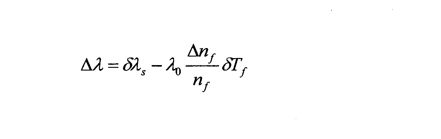
- Each temperature change ⁇ T a and ⁇ T f is expressed by the following equation from the standing wave condition.
- ⁇ 0 represents the grating reflection wavelength in the initial state.
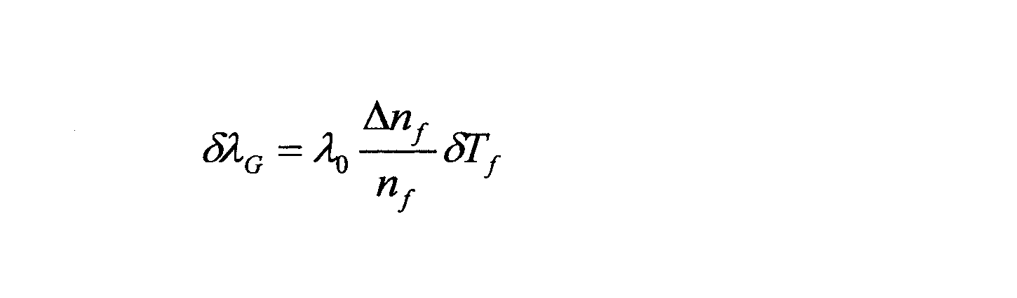
- ⁇ G in the grating reflection wavelength is expressed by the following equation.
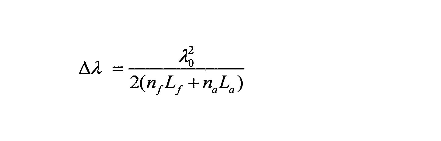
- the longitudinal mode interval ⁇ is approximately expressed by the following equation.
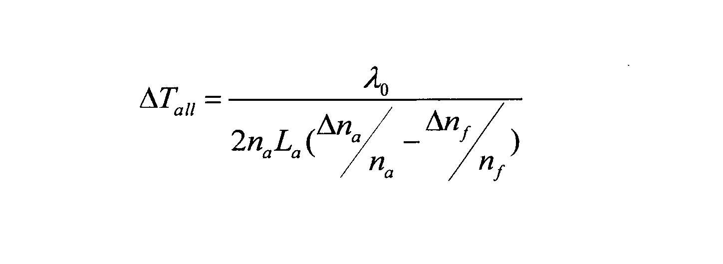
- Mathematical formula 5 is established from mathematical formulas 3 and 4.
- Mode hop is a phenomenon in which the oscillation mode (longitudinal mode) in the resonator changes from one mode to another.
- the gain and resonator conditions change, the laser oscillation wavelength changes, and the problem arises that optical power fluctuates, which is called kink. Therefore, in the case of an FP type GaAs semiconductor laser, the wavelength usually changes with a temperature coefficient of 0.3 nm / ° C., but when a mode hop occurs, a larger fluctuation occurs. At the same time, the output fluctuates by 5% or more.
- Patent Document 6 in order to make the temperature independent, the conventional resonator structure is left as it is, and stress is applied to the optical waveguide layer to compensate for the temperature coefficient due to thermal expansion, thereby realizing temperature independence. is doing. For this reason, a metal plate is attached to the element, and a layer for adjusting the temperature coefficient is added to the waveguide. For this reason, there exists a problem that a resonator structure becomes still larger.
- the present inventor has disclosed an external resonator type laser structure using an optical waveguide grating element in Patent Document 7.
- Patent Document 7 when the full width at half maximum ⁇ G of the reflection characteristic of the grating element satisfies a specific equation, laser oscillation with high wavelength stability and no power fluctuation is possible without temperature control.
- the coupling efficiency is 50% or more and the allowable axis deviation is about ⁇ 1 ⁇ m.
- the inventor determines the thickness of the optical material layer in the incident portion and the width of the ridge-type optical waveguide by the mode field diameter of the laser light emitted from the light source (vertical direction, horizontal direction). ) Tried to set larger than.
- the width of the ridge-type optical waveguide was tried to be 1.5 times or more the mode field diameter in the horizontal direction of the laser light.
- the thickness of the optical material layer was tried to be 1.5 times or more the mode field diameter in the vertical direction of the laser beam.
- the lateral mode of the light source is a single mode, and the spot diameter is 0.5 ⁇ m to 2 ⁇ m in the vertical direction and 1 ⁇ m to 6 ⁇ m in the horizontal direction.
- the thickness of the optical material layer at the incident portion is such that W inv / ⁇ is 2 or more. If the optical material layer is too thick, the coupling loss increases, so W inv / ⁇ is preferably 3 or less.
- the width of the ridge-type optical waveguide at the incident portion in the wavelength range of 0.7 ⁇ m to 1.1 ⁇ m is preferably 5 ⁇ m or more from the viewpoint of increasing the axial deviation tolerance, and the coupling loss increases. Is preferred.
- An object of the present invention is to improve the wavelength stability of an external resonator type laser using a Bragg grating while increasing the axial deviation tolerance between the laser light from the light source and the optical waveguide of the grating element.
- the grating element according to the present invention is Support substrate, An optical material layer provided on the support substrate; A ridge type optical waveguide provided on the optical material layer and having an incident surface on which laser light is incident and an output end for emitting outgoing light of a desired wavelength, and a Bragg grating made of irregularities formed in the ridge type optical waveguide
- the ridge-type optical waveguide includes an incident portion provided between the incident surface and the Bragg grating, and a tapered portion provided between the incident portion and the Bragg grating, and at least the Bragg grating Propagating light propagates in a single mode in the grating, the width of the ridge-type optical waveguide in the incident part is larger than the width of the ridge-type optical waveguide in the Bragg grating, and the width of the ridge-type optical waveguide in the tapered part is It is characterized by being smaller from the incident part toward the Bragg grating, and satisfying the following expressions (1) to (4).
- n b 0.8 nm ⁇ ⁇ G ⁇ 6.0 nm (1) 10 ⁇ m ⁇ L b ⁇ 300 ⁇ m (2) 20 nm ⁇ td ⁇ 250 nm (3) n b ⁇ 1.8 (4)
- ⁇ G is the full width at half maximum at the Bragg reflectivity peak of the Bragg grating.
- L b is the length of the Bragg grating.
- t d is the depth of the irregularities constituting the Bragg grating.
- n b is the refractive index of the material constituting the optical material layer.
- the present invention also provides: Support substrate, An optical material layer provided on the support substrate; A ridge type optical waveguide provided on the optical material layer and having an incident surface on which laser light is incident and an output end for emitting outgoing light of a desired wavelength, and a Bragg grating made of irregularities formed in the ridge type optical waveguide
- the ridge-type optical waveguide includes an incident portion provided between the incident surface and the Bragg grating, and a tapered portion provided between the incident portion and the Bragg grating, and at least the Bragg grating Propagating light propagates in a single mode in the grating, the width of the ridge-type optical waveguide in the incident part is larger than the width of the ridge-type optical waveguide in the Bragg grating, and the width of the ridge-type optical waveguide in the tapered part is It is reduced from the incident part toward the Bragg grating, and the relations of the following formulas (1) to (3) are satisfied, and the material constituting the optical material layer is gallium arsenide, lithium
- ⁇ G is the full width at half maximum at the Bragg reflectivity peak of the Bragg grating.
- L b is the length of the Bragg grating.
- t d is the depth of the irregularities constituting the Bragg grating.
- the present invention also relates to an external resonator type light emitting device including a light source that oscillates a semiconductor laser beam and a grating element that constitutes the light source and an external resonator,
- the light source includes an active layer that oscillates the semiconductor laser light, and the grating element is the above-described one.
- quartz has a small temperature coefficient of refractive index, so d ⁇ G / dT is small and
- DELTA temperature range
- the temperature coefficient of the refractive index can be increased and d ⁇ G / dT can be increased. Therefore,
- the full width at half maximum ⁇ G at the peak of the Bragg reflectivity is set larger.
- ⁇ G can be set to 0.8 nm or more and 6 nm or less.
- the number of longitudinal modes can be adjusted to 2-5. That is, the wavelengths satisfying the phase condition are discrete, and when the number of longitudinal modes in ⁇ G is 2 or more and 5 or less, mode hops are repeated in ⁇ G , and It will not come off. For this reason, it has been found that a large mode hop does not occur, so that the wavelength stability can be increased and the optical power fluctuation can be suppressed.
- the width of the ridge-type optical waveguide at the incident portion is made larger than the horizontal mode field diameter of the laser light, for example, 1.5 times or more, the tolerance of the axis deviation with the light source can be increased.
- the width of the optical waveguide is increased, the propagation light becomes multimode in the Bragg grating, so that the wavelength stability is impaired.
- the ridge type optical waveguide width in the Bragg grating is relatively reduced, and a taber portion having a small ridge type optical waveguide width is provided between the incident portion and the Bragg grating. This has succeeded in improving the off-axis tolerance under the condition that the propagating light is single mode in the Bragg grating.
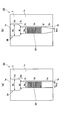
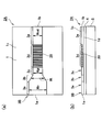
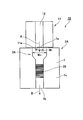
- FIGS. 1A and 1B are plan views schematically showing the grating elements 2A and 2B, respectively.
- (A) is a plan view schematically showing the grating element 2A
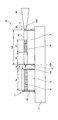
- (b) is a side view schematically showing the grating element 2A.
- (A) is a plan view schematically showing the grating element 2B
- (b) is a side view schematically showing the grating element 2B.
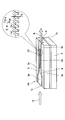
- It is a perspective view of a grating element.
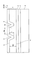
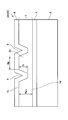
- It is a cross-sectional view of a grating element.
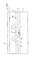
- It is a cross-sectional view of another grating element.
- the grating elements 2A and 2B are provided with an optical material layer 1 having an incident surface 1a on which laser light is incident and an emission surface 1b that emits emitted light of a desired wavelength. It has been.
- the optical material layer 1 ridge type optical waveguides 3A and 3B are provided.
- the ridge type optical waveguide 3A includes an incident portion 3a, a tapered portion 3b, a connecting portion 3c, a grating portion 3d, and an emitting portion 3e, and a Bragg grating 20 is formed in the grating portion 3d.
- the width of the emission part 3e is constant.
- the ridge-type optical waveguide 3B includes an incident portion 3a, a tapered portion 3b, a connecting portion 3c, a grating portion 3d, an emitting portion 3e, and a connecting portion 3f between the grating portion and the emitting portion 3e.
- the Bragg grating 20 is formed.
- the width of the connecting portion 3f is constant, but the width of the emitting portion 3e is gradually reduced as it approaches the emitting surface.
- the optical material layer 1 is formed on the support substrate 5 with the lower clad layer 4 interposed therebetween. 1c is an upper surface.
- the clad layer may be a material having a refractive index smaller than that of the optical material layer, and may be an adhesive layer. In the case of the adhesive layer, the bottom surface 1 d of the optical material layer is bonded onto the support substrate 5.
- the optical material layer 1 is formed on the support substrate 5 with the lower clad layer 4 interposed therebetween. 1c is an upper surface.
- the lower clad layer may be a material having a refractive index smaller than that of the optical material layer, and may be an adhesive layer. In the case of the adhesive layer, the bottom surface 1 d of the optical material layer is bonded onto the support substrate 5.
- FIG. 4 schematically shows a perspective view of the grating element 2A.
- the grating element 4B is substantially the same.
- FIG. 5, FIG. 6, and FIG. 7 show cross sections obtained by cutting the grating element with a Bragg grating, respectively.
- the optical material layer 1 is formed on the support substrate 5 via the adhesive layer 7 and the lower buffer layer 4, and the upper buffer layer 8 is formed on the optical material layer 1.
- a pair of ridge grooves 9 are formed in the optical material layer 1, and a grating portion 3 d of a ridge type optical waveguide is formed between the ridge grooves 9.
- the Bragg grating may be formed on the upper surface 1c side, or may be formed on the bottom surface 1d side. From the viewpoint of reducing variations in the shapes of the Bragg grating and the ridge groove, it is preferable to provide the Bragg grating and the ridge groove 9 on the opposite side of the substrate by forming the Bragg grating on the flat bottom surface 1d side.
- optical material layer 1 is formed on the lower side of the support substrate 5 via the buffer layer 4.
- An upper buffer layer 8 is formed on the optical material layer 1.
- the optical material layer 1 is formed on the support substrate 5 via the adhesive layer 7 and the lower buffer layer 4, and the upper buffer layer 8 is formed on the optical material layer 1.
- a pair of ridge grooves 9 are formed on the support substrate 5 side of the optical material layer 1, and a ridge type optical waveguide 3 d is formed between the ridge grooves 9.
- the Bragg grating may be formed on the flat top surface 1c side, or may be formed on the bottom surface 1d side having the ridge groove.
- the Bragg grating and the ridge groove are provided on the opposite side of the substrate by forming the Bragg grating on the flat upper surface 1c side.
- the upper buffer layer 8 may be omitted, and in this case, the air layer can directly contact the grating.
- the difference in refractive index can be increased without the presence of a grating groove, and the reflectance can be increased with a short grating length.
- the support substrate 5 has a higher refractive index than the optical material layer 1, it is preferable that the upper buffer layer is formed from the viewpoint of reducing the propagation loss of the waveguide.
- the 8 and 9 includes a light source 11 that oscillates laser light and a grating element 2A.
- the light source 11 and the grating element 2 ⁇ / b> A are mounted on the common substrate 17.
- the light source 11 includes an active layer 12 that oscillates semiconductor laser light.
- the active layer 12 is provided on the substrate 15.
- a reflective film 16 is provided on the outer end face of the light source, and an antireflective layer 13A is formed on the end face of the active layer 12 on the grating element side.
- Reference numeral 13B denotes an antireflective film provided on the incident surface side of the optical material layer 1
- reference numeral 13C denotes an antireflective film provided on the output surface side of the optical material layer 1.
- the reflectance of the non-reflective layers 13A, 13B, and 13C may be a value smaller than the grating reflectance, and is preferably 0.1% or less. However, as long as the reflectance at the end face is smaller than the grating reflectance, the non-reflective layer may be omitted, and a reflective film may be provided instead of the non-reflective layer.
- the oscillation wavelength of the laser light is determined by the wavelength reflected by the Bragg grating. If the reflected light from the Bragg grating and the reflected light from the end face of the active layer on the grating element side exceed the laser gain threshold, the oscillation condition is satisfied. Thereby, a laser beam with high wavelength stability can be obtained.
- the feedback amount from the grating may be increased.
- the reflectance of the grating is preferably larger than the reflectance at the end face of the active layer.
- a laser with a highly reliable GaAs-based or InP-based material is suitable.
- a GaAs laser that oscillates near a wavelength of 1064 nm is used. Since GaAs-based and InP-based lasers have high reliability, a light source such as a one-dimensionally arranged laser array can be realized. It may be a super luminescence diode or a semiconductor optical amplifier (SOA).
- the oscillation wavelength of the laser is particularly preferably 990 nm or less in order to improve wavelength stability.
- the wavelength is shortened, the refractive index change ⁇ na of the semiconductor becomes too large. Therefore, in order to improve the wavelength stability, the laser oscillation wavelength is particularly preferably 780 nm or more.
- the material and wavelength of the active layer can be selected as appropriate.
- Non-Patent Document 3 Furukawa Electric Times, January 2000, No. 105, p24-29
- the ridge-type optical waveguide is obtained by, for example, physical processing and molding by cutting with an outer peripheral blade or laser ablation processing.
- the Bragg grating can be formed by physical or chemical etching as follows.
- a metal film such as Ni, Ti, or Cr is formed on a high refractive index substrate, and windows are periodically formed by photolithography to form an etching mask.
- periodic grating grooves are formed by a dry etching apparatus such as reactive ion etching. Finally, it can be formed by removing the metal mask.
- the ridge type optical waveguide can also be formed in the same manner as the grating groove.
- one or more metals selected from the group consisting of magnesium (Mg), zinc (Zn), scandium (Sc), and indium (In) are used to further improve the optical damage resistance of the optical waveguide. Elements may be included, in which case magnesium is particularly preferred.
- the crystal can contain a rare earth element as a doping component. As the rare earth element, Nd, Er, Tm, Ho, Dy, and Pr are particularly preferable.
- the material of the adhesive layer may be an inorganic adhesive, an organic adhesive, or a combination of an inorganic adhesive and an organic adhesive.
- the optical material layer may be formed by forming a film on the support substrate by a thin film forming method.
- a thin film forming method include sputtering, vapor deposition, and CVD.
- the optical material layer 11 is directly formed on the support base.
- the optical material layer can be formed after the lower buffer layer is formed on the support substrate.
- the specific material of the support substrate is not particularly limited, and examples thereof include glass such as lithium niobate, lithium tantalate, and quartz glass, quartz, and Si.
- the lower cladding layer is essential, but it is preferable to provide the upper cladding layer from the viewpoint of reducing the waveguide loss.
- the lower and upper cladding layers may be the lower and upper buffer layers, respectively, and their refractive indices are lower than the refractive index of the optical material layer.
- the reflectance of the non-reflective layer needs to be equal to or lower than the grating reflectivity, and as a film material to be formed on the non-reflective layer, a film laminated with an oxide such as silicon dioxide, tantalum pentoxide, magnesium fluoride, Metals can also be used.
- each end face of the light source element and the grating element may be cut obliquely in order to suppress the end face reflection.
- the grating element and the support substrate are bonded and fixed in the example of FIG. 2, they may be directly bonded.
- a single layer film made of a material having a refractive index lower than that of the material constituting the optical material layer is formed on at least one of the entrance surface and the exit surface.
- the thickness of such a single layer film does not need to be determined exactly as in the AR coating, and end face reflection can be reduced simply by forming a single layer film.
- the degree of reflection suppression may be reduced or eliminated depending on the relationship between the refractive index and the thickness between the multilayer films, and it is necessary to control the thickness of each layer of the multilayer film. Therefore, the single layer film is superior. Thereby, the end surface reflectance of the grating element can be surely reduced as compared with the case where there is no single layer film.
- the thickness of the single layer film is preferably 1 ⁇ m or less.
- the grating element 2A is optically coupled to the light source 11, and the optical waveguide 22 of the separate optical waveguide substrate 21 is optically coupled to the emission surface of the emission part 3e of the grating element 2A. Is bound to.
- the grating element 2B is optically coupled to the light source 11, and the optical waveguide 22 of the separate optical waveguide substrate 21 is optically coupled to the emission surface of the emission part 3e of the grating element 2B. Is bound to.
- the light source 11 and the grating element 22 are mounted on a common substrate 24. It is also possible to provide the adhesive layers 7 and 25.
- the ridge type optical waveguide 23A of the grating element 22 includes an incident portion 23a, a tapered portion 23b, a grating portion 23d, and an emitting portion 23e, and a Bragg grating 20 is formed in the grating portion 23d.
- the optical waveguide width W in the entrance portion 23a is larger than the optical waveguide width W gr in a Bragg grating.
- Optical waveguide width W t of the tapered portion 23b is monotonically decreases from W in to W gr. Further, in the present embodiment, the optical waveguide width W out of the exit portion 23e is constant.
- the optical material layer thickness W inv at the incident portion 23a is larger than the optical material layer thickness W grv at the Bragg grating.
- the optical material layer thickness W tv at the tapered portion 23b monotonously decreases from W inv toward W grv .
- the optical material layer thickness W outv at the emitting portion 23e is constant.
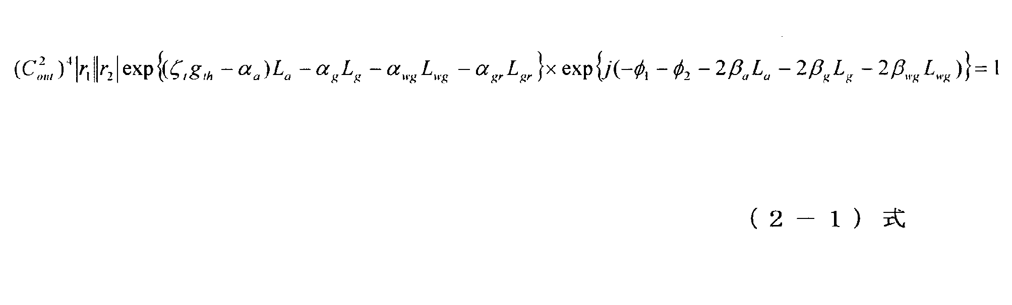
- the oscillation condition of the semiconductor laser is determined by gain condition ⁇ phase condition as shown in the following equation.
- ⁇ a , ⁇ g , ⁇ wg , ⁇ gr are the active layer, the gap between the semiconductor laser and the waveguide, the unprocessed waveguide portion on the input side, and the loss factor of the grating portion, respectively
- L a , L g , L wg , and L gr are the length of the active layer, the gap between the semiconductor laser and the waveguide, the unprocessed waveguide portion on the input side, and the grating portion, respectively
- r 1 and r 2 are mirrors
- C out is the coupling loss between the grating element and the light source
- ⁇ t g t is the gain threshold of the laser medium
- ⁇ 1 is the laser side reflection
- the phase change amount by the mirror, and ⁇ 2 is the phase change amount in the grating section.
- the gain condition when the gain ⁇ t g th (gain threshold value) of the laser medium exceeds the loss, it indicates that laser oscillation occurs.
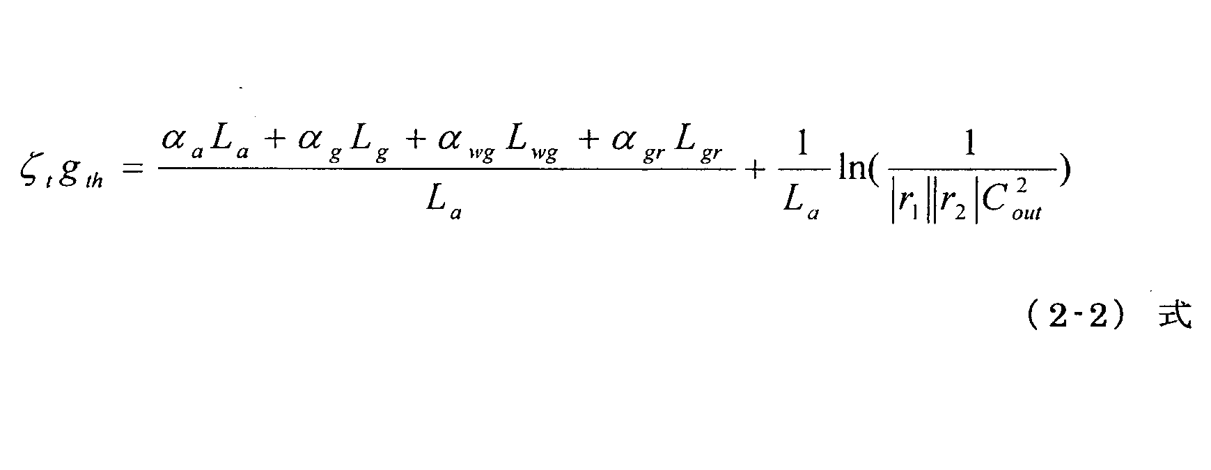
- the gain curve (wavelength dependence) of the laser medium has a full width at half maximum of 50 nm or more and has broad characteristics. Further, since the loss part (right side) has almost no wavelength dependence other than the reflectance of the grating, the gain condition is determined by the grating. For this reason, in the comparison table, the gain condition can be considered only by the grating.
- phase condition is expressed by the following equation from the equation (2-1). However, ⁇ 1 is zero.
- the external resonator type laser a product using a quartz glass waveguide or FBG as an external resonator has been commercialized.
- the length of the grating portion is 1 mm.
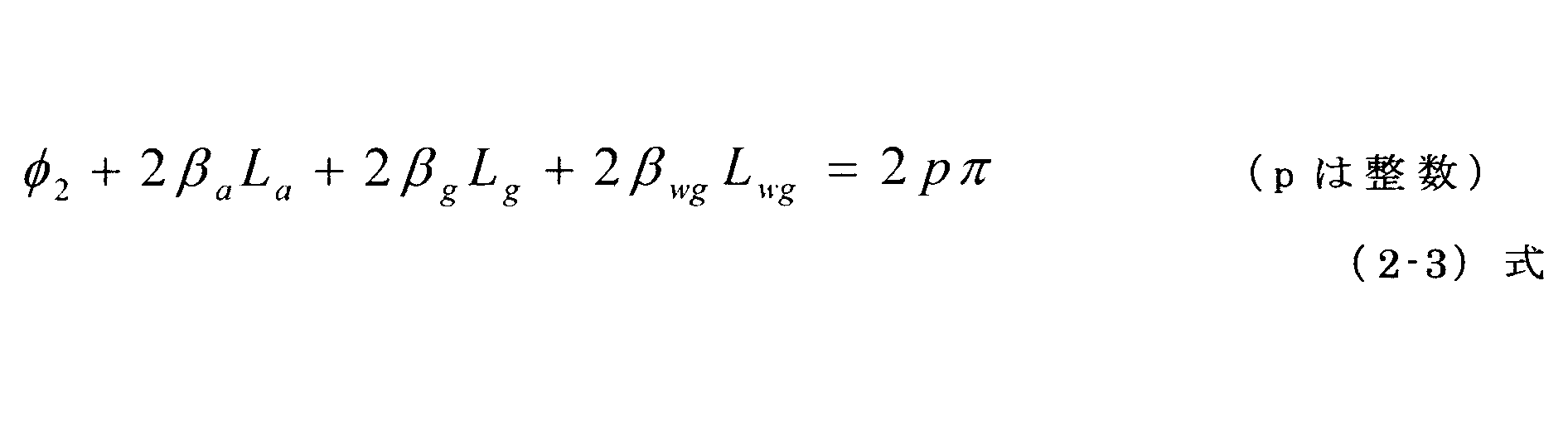
- the phase condition, the wavelength which satisfies become discrete, in ⁇ lambda G, are designed to be (2-3) equation points 2-3. For this reason, the thing with a long active layer length of a laser medium is needed, and the thing of 1 mm or more is used.
- the external cavity laser has a feature of high wavelength stability.
- ⁇ G TM is a wavelength interval (longitudinal mode interval) that satisfies the phase condition of the external cavity laser.
- the temperature T mh at which the mode hop occurs is about 5 ° C. For this reason, mode hops are likely to occur. Therefore, when a mode hop occurs, the power fluctuates based on the reflection characteristics of the grating and fluctuates by 5% or more.
- the conventional external cavity laser using the glass waveguide or FBG performs temperature control using the Peltier element.
- the present invention uses a grating element having a small denominator of the equation (2-4) as a precondition.
- the denominator of the formula (2-4) is preferably 0.03 nm / ° C. or less, and specific optical material layers include gallium arsenide (GaAs), lithium niobate (LN), lithium tantalate (LT), Tantalum oxide (Ta 2 O 5 ), zinc oxide (ZnO), aluminum oxide (Al 2 O 3 ), magnesium oxide (MgO), niobium oxide (Nb 2 O 5 ), and titanium oxide (TiO 2 ) are preferable.
- ⁇ lambda grating length in order to increase the G L b is a 100 ⁇ m example
- ⁇ G TM to be increased L a is a 250 ⁇ m example.
- FIG. 6 The present application presupposes that the temperature coefficient of the grating wavelength and the temperature coefficient of the gain curve of the semiconductor are close to each other. For this reason, a material having a refractive index of 1.8 or more is used. Further grating groove depth t d of 20nm or more, and 250nm or more, the reflectance of 3% or more, 60% or less, and 0.8nm over the full width at half maximum ⁇ lambda G, is set to 250nm or less. As a result, the resonator structure can be made compact and temperature-independence can be realized without any additional components.
- each parameter is described as follows, and each is in the category of the prior art.
- L b 3mm
- a material having a lower refractive index such as quartz, has been generally used.
- the refractive index of the material constituting the Bragg grating is increased. This is because a material with a large refractive index has a large temperature change in the refractive index, so that T mh in equation (2-4) can be increased, and the temperature coefficient d ⁇ G / dT of the grating as described above. It is because it can enlarge.
- nb is more preferably 1.9 or more.
- the upper limit of n b is not particularly preferably 4 or less since the formed grating pitch becomes too small it is difficult.
- the full width at half maximum ⁇ G at the peak of the Bragg reflectivity is set to 0.8 nm or more (Formula 1).
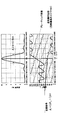
- ⁇ G is the Bragg wavelength. That is, as shown in FIGS. 15 and 16, when the reflection wavelength by the Bragg grating is taken on the horizontal axis and the reflectance is taken on the vertical axis, the wavelength at which the reflectance becomes maximum is the Bragg wavelength. In the peak centered on the Bragg wavelength, the difference between the two wavelengths at which the reflectance is half of the peak is defined as the full width at half maximum ⁇ G.
- the full width at half maximum ⁇ G at the peak of the Bragg reflectance is set to 0.8 nm or more (formula (1)). This is to make the reflectance peak broad. From this viewpoint, the full width at half maximum ⁇ G is preferably set to 1.2 nm or more, and more preferably set to 1.5 nm or more. The full width at half maximum ⁇ G is 5 nm or less, more preferably 3 nm or less, and preferably 2 nm or less.
- the length L b of the Bragg grating to 300 ⁇ m or less (formula 2: see FIG. 9).
- the length L b of the Bragg grating is a grating length in the direction of the optical axis of the light propagating through the optical waveguide. Be shorter than the Bragg grating length L b below the conventional 300 ⁇ m is a premise of the design concept of the present invention. That is, it is necessary to increase the wavelength interval (longitudinal mode interval) that satisfies the phase condition in order to make mode hopping difficult. For this purpose, it is necessary to shorten the resonator length, and to shorten the length of the grating element. From this viewpoint, it is more preferable that the Bragg grating length L b and 200 ⁇ m or less.
- Reducing the length of the grating element reduces the loss and can reduce the laser oscillation threshold. As a result, driving with low current, low heat generation, and low energy is possible.
- the length L b of the grating, in order to obtain a reflectance of 3% or more is preferably at least 5 [mu] m, in order to obtain a reflectance of 5% or more, more preferably more than 10 [mu] m.
- t d is the depth of the irregularities constituting the Bragg grating (see FIG. 4).
- ⁇ G can be set to 0.8 nm or more and 250 nm or less, and the number of longitudinal modes can be adjusted to 2 or more and 5 or less in ⁇ G.
- t d is more preferably not less than 30 nm, also more preferably 200nm or less. In order to set the full width at half maximum to 3 nm or less, 150 nm or less is preferable.
- the reflectance of the grating element is preferably set to 3% or more and 40% or less in order to promote laser oscillation. This reflectivity is more preferably 5% or more in order to further stabilize the output power, and more preferably 25% or less in order to increase the output power.
- the laser oscillation condition is established from a gain condition and a phase condition. Wavelengths satisfying the phase condition are discrete and are shown in FIG. 21, for example. That is, in the structure of the present application, the oscillation wavelength can be fixed within ⁇ G by bringing the temperature coefficient of the gain curve (0.3 nm / ° C. in the case of GaAs) close to the temperature coefficient d ⁇ G / dT of the grating.
- ⁇ lambda G number of longitudinal modes are two or more in, when present 5 or less, the oscillation wavelength repeats mode hopping in the ⁇ lambda G, large because it can reduce the probability of laser oscillation outside the ⁇ lambda G There is no mode hop, the wavelength is stable, and the output power can operate stably.
- length L a of the active layer also to 500 ⁇ m or less length L a of the active layer (Fig. 9). From this viewpoint, it is more preferable to set the length L a of the active layer and 300 ⁇ m or less.
- the length L a of the active layer with a view to increasing the output of the laser it is preferable that the 150 ⁇ m or more.
- d ⁇ G / dT is the temperature coefficient of the Bragg wavelength.
- D ⁇ TM / dT is a temperature coefficient of the wavelength that satisfies the phase condition of the external cavity laser.
- ⁇ TM is a wavelength that satisfies the phase condition of the external cavity laser, that is, a wavelength that satisfies the above-described phase condition of (Equation 2.3). This is called “vertical mode” in this specification.
- ⁇ 2 ⁇ n eff / ⁇ , where n eff is the effective refractive index of the portion, and ⁇ satisfying this is ⁇ TM .
- ⁇ 2 is the phase change of the Bragg grating, lambda TM is shown in Figure 15.
- ⁇ G TM is a wavelength interval (longitudinal mode interval) that satisfies the phase condition of the external cavity laser.
- the numerical value of the formula (6) is more preferably 0.025 or less.
- the length L WG grating element also to 600 ⁇ m or less (Fig. 9).
- LWG is preferably 400 ⁇ m or less, and more preferably 300 ⁇ m or less. Further, LWG is preferably 50 ⁇ m or more.
- the distance L g between the light exit surface of the light source and the light entrance surface of the optical waveguide is 1 ⁇ m or more and 10 ⁇ m or less (see FIG. 9). As a result, stable oscillation is possible.
- the length L m of the entrance portion and the tapered portion and 100 ⁇ m or less. This promotes stable oscillation.
- the lower limit is not particularly length L m of the propagating portion is preferably not less than 10 [mu] m, more preferably more than 20 [mu] m.
- the width W in (see FIGS. 10, 11, and 13) of the ridge-type optical waveguide at the incident portion is the mode field diameter W h in the horizontal direction of the laser light. It is preferably 1.5 times or more. Moreover, it is further preferable that the width W in the ridge type optical waveguide or less 2.5 times the horizontal direction of the mode field diameter W h of the laser beam at the incident portion.
- the thickness W inv (FIG. 13) of the optical material layer at the incident portion is 1.5 times or more the mode field diameter W v in the vertical direction of the laser light. It is preferable that Further, it is preferable that the thickness W inv of the optical material layer at the incident portion is 2.5 times or less of the mode field diameter W v in the vertical direction of the laser light.
- the horizontal and vertical mode field diameters of the laser light are measured as follows. Measure the light intensity distribution of the laser beam and measure the width where the intensity distribution is 1 / e 2 (e is the base of natural logarithm: 2.71828) with respect to the maximum value (usually equivalent to the center of the core). This is generally defined as a mode field diameter.
- the mode field is defined because the size differs between the horizontal direction and the vertical direction of the laser element. When it is concentric like an optical fiber, it is defined as a diameter.
- the light intensity distribution of the spot of the laser beam can be generally obtained by beam profile measurement using a near infrared camera or light intensity measurement by a knife edge.
- W inv / ⁇ is preferably 3 or less.
- W inv is 1.7 ⁇ m or more and 2.55 ⁇ m or less.
- the ridge type optical waveguide width Win in the incident part is larger than the ridge type optical waveguide width Wgr in the grating part.
- the width of the ridge-type optical waveguide means a distance between two corners of the cross section of the upper surface of the ridge portion constituting the optical waveguide (see FIG. 5).
- W in / W gr is preferably 1.5 or more, and more preferably 2 or more. Further, if W in / W gr is too large, the substrate radiation in the Bragg grating tends to increase, so that W in / W gr is preferably 3.5 or less.
- the width of the ridge type optical waveguide at the incident portion is preferably 5 ⁇ m or more, and preferably 10 ⁇ m or less.
- the ridge width of the grating portion is preferably 3 ⁇ or more and 5 ⁇ or less.
- the ridge width is preferably 2.55 ⁇ m or more, and preferably 4.25 ⁇ m or less.
- the incident part and the grating part are connected by a taper part.
- the tapered portion preferably be smoothly ridge width W t is reduced towards the grating portion from the incident portion, it is more preferable to reduce a linear function with respect to longitudinal direction of the element.
- the width W out of the emitting portions 3e and 23e may be the same as the width W gr of the ridge-type optical waveguide in the grating element, but may be smaller than W gr .
- W out / W gr is preferably 1.0 or less, and may be 0.5 or less, but is preferably 0.7 or more from the viewpoint of propagation efficiency.
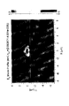
- the propagation light is converted into a single mode, so that the spot shape as shown in FIG. FIG. 17 shows a spot shape when the wavelength is 0.85 ⁇ m and the ridge width is 2 ⁇ m.
- the optical electric field leaks to the substrate, and the optical electric field on the top surface of the ridge becomes small.
- the optical electric field hardly perceives the step of the groove, and the reflectance does not increase.
- FIG. 18 shows a spot shape when the ridge type optical waveguide width is 3 ⁇ m. In this case, it can be seen that the shape is elliptical and does not leak into the substrate mode.
- the ridge width of the grating part is made too large, it will be multimoded, so there is an optimum ridge width.
- FIG. 19 shows the calculated value of the effective refractive index of the fundamental mode of the waveguide at the ridge width of 1 to 10 ⁇ m when the optical material layer thickness W inv is 2 ⁇ m and T r is 1.2 ⁇ m. From this result, the ridge widths of 1 ⁇ m and 2 ⁇ m are the rising regions of the effective refractive index and are regions close to the cutoff.
- FIG. 20 is a calculated value of propagation efficiency for the same ridge width. As a result, it can be seen that the propagation efficiency is lowered by the radiation to the substrate mode when the ridge width is 1 ⁇ m and 2 ⁇ m. In addition, the propagation efficiency tends to decrease at 5 ⁇ m or more, but this is due to the multimode.
- the thickness of the optical material layer of the grating parts 3d and 23d can be made smaller than the thickness of the optical material layer in the incident parts 3a and 23a (FIG. 3B). ), See FIG.
- the thickness of the optical material layer in the grating portions 3d and 23d / the thickness of the optical material layer in the incident portions 3a and 23a is preferably 1.0 or less. 0.7 or less, but from the viewpoint of propagation efficiency, it is preferably 0.3 or more.
- Example 1 A grating element as shown in FIGS. 1A, 2 and 4 was produced. Specifically, the optical material layer 1 was formed by depositing 1 ⁇ m of SiO 2 on the support substrate 5 made of quartz by a sputtering apparatus and further depositing 2 ⁇ m of Ta 2 O 5 . Next, Ti was formed on the optical material layer 1, and a grating pattern was produced by a photolithography technique. Thereafter, a grating groove having a pitch interval of ⁇ 205.4 nm and a length of L b of 25 ⁇ m was formed by fluorine-based reactive ion etching using the Ti pattern as a mask. Groove depth t d of the grating was set to 100 nm.
- the waveguide pattern was patterned by photolithography and reactive ion etching was performed to form a ridge groove with an incident width W in 8 ⁇ m, Tr 1 ⁇ m, a grating width W gr 3 ⁇ m, and Tr 1 ⁇ m. .
- the length from the incident surface to the grating portion start point was 25 ⁇ m.
- the input side and the output side of the element were etched to the quartz substrate by dry etching to make the end face a mirror surface.
- a single layer film of 90 nm was formed on both end surfaces by sputtering of SiO 2 .
- the reflectance of the end face was 3%.
- the element size was 1 mm wide and L wg 100 ⁇ m long.
- Optical characteristics of the grating element are measured by using a super luminescence diode (SLD), which is a broadband wavelength light source, and inputting TE mode light into the grating element and analyzing the output light with an optical spectrum analyzer. The reflection characteristics were evaluated from the characteristics.
- the reflection center wavelength of the measured element was 850 nm.
- the light source element used was an ordinary GaAs laser.
- the module After mounting the module, when driven by current control (ACC) without using a Peltier element, it oscillates at a center wavelength of 850 nm corresponding to the reflection wavelength of the grating, and the output is smaller than that without the grating element, but a 30 mW laser It was a characteristic. The fluctuation of output was stable within 1%. Further, the temperature dependence of the laser oscillation wavelength was measured in the temperature range of 20 ° C. to 40 ° C. As a result, the temperature coefficient of the oscillation wavelength was 0.05 nm / ° C.
- Example 1 A grating element having the same structure was formed by the same method as in Example 1. However, ridge groove processing was performed with a light source input portion width W in of 8 ⁇ m and T r of 1 ⁇ m and a grating portion width of W gr of 8 ⁇ m and T r of 1 ⁇ m. The length from the input end face to the grating part starting point was 25 ⁇ m.
- the input side and the output side of the element were etched to the quartz substrate by dry etching to make the end face a mirror surface.
- a single layer film of 90 nm was formed on both end surfaces by sputtering of SiO 2 .
- the reflectance of the end face was 3%.
- the element size was 1 mm wide and L wg 100 ⁇ m long.
- Optical characteristics of the grating element are measured by using a super luminescence diode (SLD), which is a broadband wavelength light source, and inputting TE mode light into the grating element and analyzing the output light with an optical spectrum analyzer.
- SLD super luminescence diode
- the reflection characteristics were evaluated from the characteristics.
- the reflection center wavelength of the measured element was 850 nm. However, reflection was measured at a plurality of wavelengths 845 nm, 840 nm, and 836 nm on the shorter wavelength side than this.
- the light source element used was an ordinary GaAs laser.
- the module When the module is mounted and driven by current control (ACC) without using a Peltier element, it oscillates at a center wavelength of 845 nm corresponding to the reflection wavelength of the grating, and the output is smaller than in the case where there is no grating element.
- the laser characteristic was 30 mW, which was almost equivalent to Further, the temperature dependence of the laser oscillation wavelength was measured in the temperature range of 20 ° C. to 40 ° C. As a result, the temperature coefficient of the oscillation wavelength was 0.05 nm / ° C., but the wavelength greatly changed to 850.4 nm around 30 ° C., and the output greatly fluctuated.
- Example 2 A grating element having the same structure was formed by the same method as in Example 1. However, ridge groove processing was performed with a light source input width W in 8 ⁇ m, Tr 1 ⁇ m, and a grating width W gr 2 ⁇ m, Tr 1 ⁇ m. The length from the input end face to the grating part starting point was 25 ⁇ m.
- the input side and the output side of the element were etched to the quartz substrate by dry etching to make the end face a mirror surface.
- a single layer film of 90 nm was formed on both end surfaces by sputtering of SiO 2 .
- the reflectance of the end face was 3%.
- the element size was 1 mm wide and L wg 100 ⁇ m long.
- Optical characteristics of the grating element are measured by using a super luminescence diode (SLD), which is a broadband wavelength light source, and inputting TE mode light into the grating element and analyzing the output light with an optical spectrum analyzer.
- SLD super luminescence diode
- the reflection characteristics were evaluated from the characteristics.
- the reflection center wavelength of the measured element was 849.5 nm.
- the light source element used was an ordinary GaAs laser.
- the module After mounting the module, when driven by current control (ACC) without using a Peltier device, it oscillates at a center wavelength of 849.5 nm corresponding to the reflection wavelength of the grating, and the output is smaller than that of Example 1 and has a laser characteristic of 10 mW there were. This was due to an increase in propagation loss. However, the fluctuation of the output was stable within 1%. Further, the temperature dependence of the laser oscillation wavelength was measured in the temperature range of 20 ° C. to 40 ° C. As a result, there was no change as in Example 1, and the temperature coefficient of the oscillation wavelength was 0.05 nm / ° C.
- Example 3 Elements as shown in FIGS. 1A and 3 were produced.
- the optical material layer 1 was formed by forming 2 ⁇ m of SiO 2 on the support substrate 5 made of quartz by a sputtering apparatus and further forming 2 ⁇ m of Ta 2 O 5 .
- Ti was formed on the optical material layer 1, and a grating pattern was produced by a photolithography technique. Thereafter, a grating groove having a pitch interval of ⁇ 205.4 nm and a length of L b of 25 ⁇ m was formed by fluorine-based reactive ion etching using the Ti pattern as a mask. Groove depth t d of the grating was set to 100 nm.
- the length from the input end face to the grating part starting point was 25 ⁇ m.
- the input portion and the taper portion were masked, and the thickness of the Ta 2 O 5 was etched by 1 ⁇ m on the entire grating portion by reactive ion etching. As a result, as shown in FIG.
- the optical material layer thickness in the grating element was made smaller than the optical material layer thickness in the incident portion and the tapered portion.
- Groove depth t d of this time the grating was set to be in 40 nm
- groove depth of the ridge waveguide was set to be 0.6 .mu.m.
- the input side and the output side of the element were etched up to the quartz substrate by dry etching to make the end face a mirror surface.
- a single layer film of 90 nm was formed on both end surfaces by sputtering of SiO 2 .
- the reflectance of the end face was 3%.
- the element size was 1 mm wide and L wg 100 ⁇ m long.
- Optical characteristics of the grating element are measured by using a super luminescence diode (SLD), which is a broadband wavelength light source, and inputting TE mode light into the grating element and analyzing the output light with an optical spectrum analyzer. The reflection characteristics were evaluated from the characteristics.
- the reflection center wavelength of the measured element was 848 nm.
- the light source element used was an ordinary GaAs laser.
- the module After mounting the module, when driven by current control (ACC) without using a Peltier element, it oscillates at a center wavelength of 848 nm corresponding to the reflection wavelength of the grating, and the output is smaller than that without the grating element, but a 30 mW laser It was a characteristic. The fluctuation of output was stable within 1%. Further, the temperature dependence of the laser oscillation wavelength was measured in the temperature range of 20 ° C. to 40 ° C. As a result, the temperature coefficient of the oscillation wavelength was 0.05 nm / ° C.
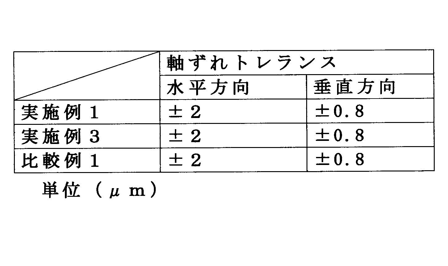
- the tolerance of the misalignment between the semiconductor laser and the grating element was measured.
- a semiconductor laser which is a light source element, and a grating element were mounted on an optical alignment device, and the optical axis was adjusted to maximize the amount of light output from the grating element. From this state, the axis was shifted in increments of 0.1 ⁇ m only in the horizontal direction, and the change in the amount of light was measured.
- the horizontal axis tolerance is defined as the amount of axis deviation when the amount of light is 25 mW.
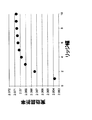
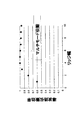
- the vertical deviation was measured to measure the amount of axial deviation. The results measured for Examples 1 and 3 and Comparative Example 1 are shown below.
- Example 2 A grating element was formed in the same manner as in Example 1, and a laser module as shown in FIG. 9 was mounted.
- the module When the module was mounted and driven by current control (ACC) without using a Peltier element, it oscillated at a center wavelength of 850 nm corresponding to the reflection wavelength of the grating, and the output was a laser characteristic of 30 mW. The fluctuation of output was stable within 1%. Further, the temperature dependence of the laser oscillation wavelength was measured in the temperature range of 20 ° C. to 40 ° C. As a result, there was no change as in Example 1, and the temperature coefficient of the oscillation wavelength was 0.05 nm / ° C.
- the module When the module was mounted and driven by current control (ACC) without using a Peltier element, it oscillated at a center wavelength of 848 nm corresponding to the reflection wavelength of the grating, and the output was a laser characteristic of 30 mW. The fluctuation of output was stable within 1%. Further, the temperature dependence of the laser oscillation wavelength was measured in the temperature range of 20 ° C. to 40 ° C. As a result, the temperature coefficient of the oscillation wavelength was 0.05 nm / ° C.
- Example 4 A grating element was formed in the same manner as in Example 1, and a laser module as shown in FIG. 9 was mounted.
- the module When the module was mounted and driven by current control (ACC) without using a Peltier element, it oscillated at a center wavelength of 848 nm corresponding to the reflection wavelength of the grating, and the output was a laser characteristic of 35 mW. The fluctuation of output was stable within 1%. Further, the temperature dependence of the laser oscillation wavelength was measured in the temperature range of 20 ° C. to 40 ° C. As a result, there was no change as in Example 1, and the temperature coefficient of the oscillation wavelength was 0.05 nm / ° C.
Landscapes
- Physics & Mathematics (AREA)
- General Physics & Mathematics (AREA)
- Optics & Photonics (AREA)
- Engineering & Computer Science (AREA)
- Microelectronics & Electronic Packaging (AREA)
- Condensed Matter Physics & Semiconductors (AREA)
- Electromagnetism (AREA)
- Optical Integrated Circuits (AREA)
- Semiconductor Lasers (AREA)
Abstract
Description
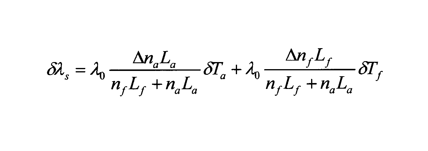
また、グレーティング反射波長の変化δλGは、下式で表される。
支持基板、
前記支持基板上に設けられた光学材料層、
前記光学材料層に設けられ、レーザ光が入射する入射面と所望波長の出射光を出射する出射端を有するリッジ型光導波路、および
このリッジ型光導波路内に形成された凹凸からなるブラッググレーティングを備えており、
前記リッジ型光導波路が、前記入射面と前記ブラッググレーティングとの間に設けられている入射部および前記入射部と前記ブラッググレーティングとの間に設けられているテーパ部を含んでおり、少なくとも前記ブラッググレーティングにおいて伝搬光がシングルモード伝搬し、前記入射部における前記リッジ型光導波路の幅が前記ブラッググレーティングにおける前記リッジ型光導波路の幅よりも大きく、前記テーパ部における前記リッジ型光導波路の幅が前記入射部から前記ブラッググレーティングに向かって小さくなっており、下記式(1)~式(4)の関係が満足されることを特徴とする。
0.8nm≦△λG≦6.0nm・・・(1)
10μm≦Lb≦300μm ・・・(2)
20nm≦td≦250nm ・・・(3)
nb≧1.8 ・・・(4)
(式(1)において、△λGは、前記ブラッググレーティングのブラッグ反射率のピークにおける半値全幅である。
式(2)において、Lbは、前記ブラッググレーティングの長さである。
式(3)において、tdは、前記ブラッググレーティングを構成する凹凸の深さである。
式(4)において、nbは、前記光学材料層を構成する材質の屈折率である。)
また,本発明は、
支持基板、
前記支持基板上に設けられた光学材料層、
前記光学材料層に設けられ、レーザ光が入射する入射面と所望波長の出射光を出射する出射端を有するリッジ型光導波路、および
このリッジ型光導波路内に形成された凹凸からなるブラッググレーティングを備えており、
前記リッジ型光導波路が、前記入射面と前記ブラッググレーティングとの間に設けられている入射部および前記入射部と前記ブラッググレーティングとの間に設けられているテーパ部を含んでおり、少なくとも前記ブラッググレーティングにおいて伝搬光がシングルモード伝搬し、前記入射部における前記リッジ型光導波路の幅が前記ブラッググレーティングにおける前記リッジ型光導波路の幅よりも大きく、前記テーパ部における前記リッジ型光導波路の幅が前記入射部から前記ブラッググレーティングに向かって小さくなっており、下記式(1)~式(3)の関係が満足され、前記光学材料層を構成する材質が、ガリウム砒素、ニオブ酸リチウム単結晶、酸化タンタル、酸化亜鉛、酸化アルミニウム、タンタル酸リチウム、酸化マグネシウム、酸化二オブおよび酸化チタンからなる群より選択されることを特徴とする、グレーティング素子。
0.8nm≦△λG≦6.0nm・・・(1)
10μm≦Lb≦300μm ・・・(2)
20nm≦td≦250nm ・・・(3)
(式(1)において、△λGは、前記ブラッググレーティングのブラッグ反射率のピークにおける半値全幅である。
式(2)において、Lbは、前記ブラッググレーティングの長さである。
式(3)において、tdは、前記ブラッググレーティングを構成する凹凸の深さである。)
前記光源が、前記半導体レーザ光を発振する活性層を備えており、前記グレーティング素子が前記のものであることを特徴とする。
(非特許文献3: 古河電工時報 平成12年1月 第105号 p24-29)
具体例として、Ni、Ti、Crなどの金属膜を高屈折率基板に成膜し、フォトリソグラフィーにより周期的に窓を形成しエッチング用マスクを形成する。その後、反応性イオンエッチングなどのドライエッチング装置で周期的なグレーティング溝を形成する。最後に金属マスクを除去することにより形成できる。
リッジ型光導波路も、グレーティング溝と同じように形成することができる。
下部、上部クラッド層は、それぞれ下部、上部バッファ層であってよく、またこれらの屈折率は、光学材料層の屈折率よりも低い。
ただし、数式は抽象的で理解しにくいので、最初に、従来技術の典型的な形態と本発明の実施形態とを端的に比較し、本発明の特徴を述べる。次いで、本発明の各条件について述べていくこととする。
ΔGTMは、外部共振器レーザの位相条件を満足する波長間隔(縦モード間隔)である。

本願は、グレーティング波長の温度係数と半導体のゲインカーブの温度係数を近づけることを前提としている。このことから屈折率が1.8以上の材料を使用することとしている。さらにグレーティングの溝深さtdを20nm以上、250nm以上とし、反射率を3%以上、60%以下で、かつその半値全幅△λGを0.8nm以上、250nm以下としている。これらにより共振器構造をコンパクトにでき、かつ付加するものをなくして温度無依存性が実現できる。特許文献6では、各パラメータは以下のように記載されており、いずれも従来技術の範疇となっている。
△λG=0.4nm
縦モード間隔△GTM=0.2nm
グレーティング長Lb=3mm
LD活性層長さLa=600μm
伝搬部の長さ=1.5mm
0.8nm≦△λG≦6.0nm・・・(1)
10μm≦Lb≦300μm ・・・(2)
20nm≦td≦250nm ・・・(3)
従来は石英などの、より屈折率の低い材料が一般的であったが、本発明の思想では、ブラッググレーティングを構成する材質の屈折率を高くする。この理由は、屈折率が大きい材料は屈折率の温度変化が大きいからであり、(2-4)式のTmhを大きくすることができ、さらに前述のようにグレーティングの温度係数dλG/dTを大きくできるからである。この観点からは、nbは1.9以上であることが更に好ましい。また、nbの上限は特にないが、グレーティングピッチが小さくなりすぎて形成が困難になることから4以下が好ましい。
また、dλTM/dTは、外部共振器レーザの位相条件を満足する波長の温度係数である。
ここで、λTMは、外部共振器レーザの位相条件を満足する波長であり、つまり前述した(2.3式)の位相条件を満足する波長である。これを本明細書では「縦モード」と呼ぶ。
(2.3)式の中のβ=2πneff/λであり、neffはその部の実効屈折率であり、これを満足するλがλTMとなる。φ2は、ブラッググレーティングの位相変化であり、λTMは図15で示される。
レーザ光の光強度分布を測定して、その強度分布が最大値(通常はコアの中心部分に相当)に対して1/e2(eは自然対数の底: 2.71828)になるところの幅のことを、一般的に、モードフィールド径と定義する。レーザ光の場合、モードフィールドはレーザ素子の水平方向と垂直方向で大きさが異なるために、それぞれ定義する。光ファイバのように同心円である場合には直径として定義される。
レーザ光の波長が0.85μmの場合に、Winvは1.7μm以上、2.55μm以下となる。
図1(a)、図2、図4に示すようなグレーティング素子を作製した。
具体的には、石英からなる支持基板5にスパッタ装置にてSiO2を1μm成膜し、さらにTa2O5を2μm成膜して光学材料層1を形成した。次に、光学材料層1上にTiを成膜して、フォトリソグラフィ技術によりグレーティングパターンを作製した。その後、Tiパターンをマスクにしてフッ素系の反応性イオンエッチングにより、ピッチ間隔Λ205.4nm、長さLb 25μmのグレーティング溝を形成した。グレーティングの溝深さtdは100nmとした。さらに導波路のパターンをフォトリソグラフィ技術にてパターニングして反応性イオンエッチングにより、入射部の幅Win8μm、Tr1μm、グレーティング部の幅Wgr3μm、Tr1μmのリッジ溝加工を実施した。入射面からグレーティング部開始点までの長さは25μmとした。
測定した素子の反射中心波長は850nmであった。
光源素子仕様:
中心波長: 847nm
出力: 50mW
半値幅: 0.1nm
レーザ素子長 250μm
実装仕様:
Lg: 1μm
Win: 8μm
Wh: 3μm
Win/Wh: 2.7
Winv: 2μm
Wv: 1μm
Winv/Wv: 2
実施例1と同様な方法で同様な構造のグレーティング素子を形成した。ただし、光源入力部の幅Win8μm、Tr1μm、グレーティング部の幅Wgr8μm、Tr1μmのリッジ溝加工を実施した。入力端面からグレーティング部開始点までの長さは25μmとした。
測定した素子の反射中心波長は850nmであった。しかし、これよりも短波長側に複数の波長845nm、840nm、836nmで反射が測定された。
光源素子仕様:
中心波長: 847nm
出力: 50mW
半値幅: 0.1nm
レーザ素子長 250μm
実装仕様:
Lg: 1μm
Win: 8μm
Wh: 3μm
Win/Wh: 2.7
Winv: 2μm
Wv: 1μm
Winv/Wv: 2
実施例1と同様な方法で同様な構造のグレーティング素子を形成した。ただし、光源入力部の幅Win8μm、Tr1μm、グレーティング部の幅Wgr2μm、Tr1μmのリッジ溝加工を実施した。入力端面からグレーティング部開始点までの長さは25μmとした。
測定した素子の反射中心波長は849.5nmであった。
光源素子仕様:
中心波長: 847nm
出力: 50mW
半値幅: 0.1nm
レーザ素子長 250μm
実装仕様:
Lg: 1μm
Win: 8μm
Wh: 3μm
Win/Wh: 2.7
Winv: 2μm
Wv: 1μm
Winv/Wv: 2
図1(a)、図3に示すような素子を作製した。
具体的には、石英からなる支持基板5にスパッタ装置にてSiO2を2μm成膜し、さらにTa2O5を2μm成膜して光学材料層1を形成した。次に、光学材料層1上にTiを成膜して、フォトリソグラフィ技術によりグレーティングパターンを作製した。その後、Tiパターンをマスクにしてフッ素系の反応性イオンエッチングにより、ピッチ間隔Λ205.4nm、長さLb 25μmのグレーティング溝を形成した。グレーティングの溝深さtdは100nmとした。さらに導波路のパターンをフォトリソグラフィ技術にてパターニングして反応性イオンエッチングにより、入射部の幅Win8μm、Tr1.6μm、グレーティング部の幅Wgr3μm、Tr1.6μmのリッジ溝加工を実施した。入力端面からグレーティング部開始点までの長さは25μmとした。
その後、入力部とテーパ部をマスキングしてグレーティング部を反応性イオンエッチングにて全体にTa2O5の厚みを1μmエッチングした。これによって、図3(b)に示すように、グレーティング素子における光学材料層厚さを入射部およびテーパ部における光学材料層厚さよりも小さくした。このときグレーティングの溝深さtdは40nmになるようにし、リッジ導波路の溝深さは0.6μmとなるようにした。
測定した素子の反射中心波長は848nmであった。
光源素子仕様:
中心波長: 847nm
出力: 50mW
半値幅: 0.1nm
レーザ素子長 250μm
実装仕様:
Lg: 1μm
Win: 8μm
Wh: 3μm
Win/Wh: 2.7
Winv: 2μm
Wv: 1μm
Winv/Wv: 2
Wgrv: 1μm
Winv/Wgrv: 2
ときの軸ずれ量と定義する。同じように垂直方向についても測定し軸ずれ量を測定した。
実施例1、3、比較例1について測定した結果を以下に示す。
実施例1と同様にグレーティング素子を形成し、図9に示すようなレーザモジュールを実装した。
光源素子仕様:
中心波長: 847nm
出力: 50mW
半値幅: 0.1nm
レーザ素子長 250μm
実装仕様:
Lg: 1μm
Win: 3μm
Wh: 3μm
Win/Wh: 1
Winv: 2μm
Wv: 1μm
Winv/Wv: 2
図1(a)、図3に示すような素子を作製し、図9に示すようなレーザモジュールを実装した。
光源素子仕様:
中心波長: 847nm
出力: 50mW
半値幅: 0.1nm
レーザ素子長 250μm
実装仕様:
Lg: 1μm
Win: 3μm
Wh: 3μm
Win/Wh: 1
Winv: 2μm
Wv: 1μm
Winv/Wv: 2
Wgrv: 1μm
Winv/Wgrv: 2
実施例1と同様にグレーティング素子を形成し、図9に示すようなレーザモジュールを実装した。
光源素子仕様:
中心波長: 847nm
出力: 50mW
半値幅: 0.1nm
レーザ素子長 250μm
実装仕様:
Lg: 1μm
Win: 3μm
Wh: 3μm
Win/Wh: 1
Winv: 1μm
Wv: 1μm
Winv/Wv: 1
Claims (12)
- 支持基板、
前記支持基板上に設けられた光学材料層、
前記光学材料層に設けられ、レーザ光が入射する入射面と所望波長の出射光を出射する出射端を有するリッジ型光導波路、および
このリッジ型光導波路内に形成された凹凸からなるブラッググレーティングを備えており、
前記リッジ型光導波路が、前記入射面と前記ブラッググレーティングとの間に設けられている入射部および前記入射部と前記ブラッググレーティングとの間に設けられているテーパ部を含んでおり、少なくとも前記ブラッググレーティングにおいて伝搬光がシングルモード伝搬し、前記入射部における前記リッジ型光導波路の幅が前記ブラッググレーティングにおける前記リッジ型光導波路の幅よりも大きく、前記テーパ部における前記リッジ型光導波路の幅が前記入射部から前記ブラッググレーティングに向かって小さくなっており、下記式(1)~式(4)の関係が満足されることを特徴とする、グレーティング素子。
0.8nm≦△λG≦6.0nm・・・(1)
10μm≦Lb≦300μm ・・・(2)
20nm≦td≦250nm ・・・(3)
nb≧1.8 ・・・(4)
(式(1)において、△λGは、前記ブラッググレーティングのブラッグ反射率のピークにおける半値全幅である。
式(2)において、Lbは、前記ブラッググレーティングの長さである。
式(3)において、tdは、前記ブラッググレーティングを構成する凹凸の深さである。
式(4)において、nbは、前記光学材料層を構成する材質の屈折率である。)
- 支持基板、
前記支持基板上に設けられた光学材料層、
前記光学材料層に設けられ、レーザ光が入射する入射面と所望波長の出射光を出射する出射端を有するリッジ型光導波路、および
このリッジ型光導波路内に形成された凹凸からなるブラッググレーティングを備えており、
前記リッジ型光導波路が、前記入射面と前記ブラッググレーティングとの間に設けられている入射部および前記入射部と前記ブラッググレーティングとの間に設けられているテーパ部を含んでおり、少なくとも前記ブラッググレーティングにおいて伝搬光がシングルモード伝搬し、前記入射部における前記リッジ型光導波路の幅が前記ブラッググレーティングにおける前記リッジ型光導波路の幅よりも大きく、前記テーパ部における前記リッジ型光導波路の幅が前記入射部から前記ブラッググレーティングに向かって小さくなっており、下記式(1)~式(3)の関係が満足され、前記光学材料層を構成する材質が、ガリウム砒素、ニオブ酸リチウム単結晶、酸化タンタル、酸化亜鉛、酸化アルミニウム、タンタル酸リチウム、酸化マグネシウム、酸化二オブおよび酸化チタンからなる群より選択されることを特徴とする、グレーティング素子。
0.8nm≦△λG≦6.0nm・・・(1)
10μm≦Lb≦300μm ・・・(2)
20nm≦td≦250nm ・・・(3)
(式(1)において、△λGは、前記ブラッググレーティングのブラッグ反射率のピークにおける半値全幅である。
式(2)において、Lbは、前記ブラッググレーティングの長さである。
式(3)において、tdは、前記ブラッググレーティングを構成する凹凸の深さである。)
- 前記入射部における前記光学材料層の厚さが前記ブラッググレーティングにおける前記光学材料層の厚さよりも大きく、前記テーパ部における前記光学材料層の厚さが前記入射部から前記ブラッググレーティングに向かって小さくなっていることを特徴とする、請求項1または2記載の素子。
- 前記レーザ光の波長がλであり、少なくとも前記入射部における前記光学材料層の厚さがWinvであり、Winv/λが2以上、3以下であり、前記ブラッググレーティングにおける前記リッジ型光導波路の幅が3λ以上、5λ以下であることを特徴とする、請求項1~3のいずれか一つの請求項に記載の素子。
- 前記ブラッググレーティングにおける前記光学材料層の厚さWgrv/前記レーザ光の波長λが1以上、2以下であることを特徴とする。請求項4記載の素子。
- 前記入射面と前記出射端との少なくとも一方に、前記光学材料層を構成する前記材質の屈折率よりも低い屈折率を有する材質からなる単層膜が形成されていることを特徴とする、請求項1~5のいずれか一つの請求項に記載の素子。
- レーザ光を発振する光源、およびこの光源と外部共振器を構成するグレーティング素子を備える外部共振器型発光装置であって、
前記光源が、前記レーザ光を発振する活性層を備えており、前記グレーティング素子が、請求項1~6のいずれか一つの請求項に記載のグレーティング素子であることを特徴とする、外部共振器型発光装置。 - 前記入射部における前記リッジ型光導波路の幅が前記レーザ光の水平方向のモードフィールド径の1.5倍以上であることを特徴とする、請求項7記載の装置。
- 前記入射部における前記光学材料層の厚さが、前記レーザ光の垂直方向のモードフィールド径の1.5倍以上であることを特徴とする、請求項7または8記載の装置。
- 下記式(5)の関係が満足されることを特徴とする、請求項7~9のいずれか一つの請求項に記載の装置。
LWG ≦500μm ・・・(5)
(式(5)において、LWGは、前記グレーティング素子の長さである。)
- 前記半値全幅△λGの中に、レーザ発振の位相条件が満足可能な波長が2以上、5以下存在することを特徴とする、請求項7~10のいずれか一つの請求項に記載の装置。
- 下記式(6)の関係が満足されることを特徴とする、請求項7~11のいずれか一つの請求項に記載の装置。
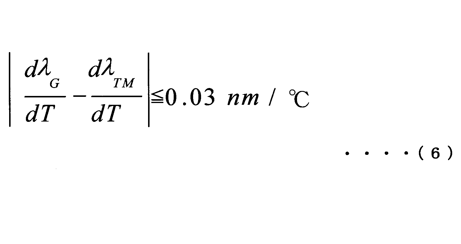
dλTM/dTは、外部共振器レーザの位相条件を満足する波長の温度係数である。)
Priority Applications (4)
| Application Number | Priority Date | Filing Date | Title |
|---|---|---|---|
| DE112015002094.2T DE112015002094B4 (de) | 2014-05-01 | 2015-04-13 | Lichtemittierende Vorrichtung des äußeren Resonatortyps |
| CN201580020713.7A CN106233175B (zh) | 2014-05-01 | 2015-04-13 | 外部谐振器型发光装置 |
| JP2015533779A JP6554035B2 (ja) | 2014-05-01 | 2015-04-13 | グレーティング素子および外部共振器型発光装置 |
| US15/333,487 US10074962B2 (en) | 2014-05-01 | 2016-10-25 | Grating element and external resonator type light emitting device |
Applications Claiming Priority (2)
| Application Number | Priority Date | Filing Date | Title |
|---|---|---|---|
| JP2014-094789 | 2014-05-01 | ||
| JP2014094789 | 2014-05-01 |
Related Child Applications (1)
| Application Number | Title | Priority Date | Filing Date |
|---|---|---|---|
| US15/333,487 Continuation US10074962B2 (en) | 2014-05-01 | 2016-10-25 | Grating element and external resonator type light emitting device |
Publications (1)
| Publication Number | Publication Date |
|---|---|
| WO2015166794A1 true WO2015166794A1 (ja) | 2015-11-05 |
Family
ID=54358529
Family Applications (1)
| Application Number | Title | Priority Date | Filing Date |
|---|---|---|---|
| PCT/JP2015/061385 Ceased WO2015166794A1 (ja) | 2014-05-01 | 2015-04-13 | グレーティング素子および外部共振器型発光装置 |
Country Status (5)
| Country | Link |
|---|---|
| US (1) | US10074962B2 (ja) |
| JP (1) | JP6554035B2 (ja) |
| CN (1) | CN106233175B (ja) |
| DE (1) | DE112015002094B4 (ja) |
| WO (1) | WO2015166794A1 (ja) |
Cited By (3)
| Publication number | Priority date | Publication date | Assignee | Title |
|---|---|---|---|---|
| CN106483600A (zh) * | 2016-11-21 | 2017-03-08 | 华中科技大学 | 一种具有大制作容差的超短垂直波导耦合器 |
| CN108919414A (zh) * | 2018-07-02 | 2018-11-30 | 中国科学院半导体研究所 | 一种soi平面波导布拉格光栅及制作方法 |
| JP2019008255A (ja) * | 2017-06-28 | 2019-01-17 | 京セラ株式会社 | 光導波路フィルタ及び光源装置 |
Families Citing this family (3)
| Publication number | Priority date | Publication date | Assignee | Title |
|---|---|---|---|---|
| DE102016115723A1 (de) * | 2016-08-24 | 2018-03-01 | Forschungsverbund Berlin E.V. | Wellenleiterstruktur und optisches System mit Wellenleiterstruktur |
| WO2018100868A1 (ja) * | 2016-12-02 | 2018-06-07 | 日本碍子株式会社 | 光学素子及びその製造方法 |
| CN115411612B (zh) * | 2022-09-05 | 2023-08-01 | 武汉敏芯半导体股份有限公司 | 窄线宽半导体激光器及其制备方法 |
Citations (4)
| Publication number | Priority date | Publication date | Assignee | Title |
|---|---|---|---|---|
| JPH1098230A (ja) * | 1996-09-25 | 1998-04-14 | Nippon Telegr & Teleph Corp <Ntt> | 周波数安定化レーザ |
| JP2002185076A (ja) * | 2000-12-15 | 2002-06-28 | Hitachi Cable Ltd | ハイブリッドdbrレーザ及びそのアレイ |
| JP3667209B2 (ja) * | 2000-08-01 | 2005-07-06 | 住友電気工業株式会社 | 半導体レーザ |
| JP4271704B2 (ja) * | 2004-04-09 | 2009-06-03 | パナソニック株式会社 | コヒーレント光源および光学装置 |
Family Cites Families (16)
| Publication number | Priority date | Publication date | Assignee | Title |
|---|---|---|---|---|
| JPS49128689A (ja) | 1973-04-06 | 1974-12-10 | ||
| JPS56148880A (en) | 1980-04-21 | 1981-11-18 | Nec Corp | Single longitudinal mode semiconductor laser |
| US5513196A (en) * | 1995-02-14 | 1996-04-30 | Deacon Research | Optical source with mode reshaping |
| JP2000082864A (ja) | 1998-09-04 | 2000-03-21 | Nippon Telegr & Teleph Corp <Ntt> | レーザ装置 |
| US6285702B1 (en) * | 1999-03-05 | 2001-09-04 | Coherent, Inc. | High-power external-cavity optically-pumped semiconductor laser |
| JP2002134833A (ja) | 2000-10-23 | 2002-05-10 | Nippon Telegr & Teleph Corp <Ntt> | 温度無依存型レーザ |
| US6944192B2 (en) | 2001-03-14 | 2005-09-13 | Corning Incorporated | Planar laser |
| US20030174956A1 (en) * | 2002-03-13 | 2003-09-18 | Jean-Francois Viens | Polarization insensitive modal field transformer for high index contrast waveguide devices |
| DE10303927B4 (de) * | 2003-01-31 | 2005-03-31 | Fraunhofer-Gesellschaft zur Förderung der angewandten Forschung e.V. | Sonde für ein optisches Nahfeldmikroskop mit verbesserter Streulichtunterdrückung und Verfahren zu deren Herstellung |
| JP2006222399A (ja) | 2005-02-14 | 2006-08-24 | Hamamatsu Photonics Kk | 半導体レーザ装置 |
| KR100670827B1 (ko) * | 2005-12-10 | 2007-01-19 | 한국전자통신연구원 | 광흡수층을 중심으로 경사형 굴절율 분포를 갖는 도파로형p-i-n 포토다이오드 |
| JP5326601B2 (ja) * | 2009-01-23 | 2013-10-30 | 富士通株式会社 | 光送信装置 |
| KR101038264B1 (ko) * | 2009-06-12 | 2011-06-01 | (주)엠이엘 | 외부공진형 파장가변 레이저 모듈 |
| WO2013034813A2 (en) | 2011-09-07 | 2013-03-14 | Epicrystals Oy | Wavelength conversion unit |
| JP2013120999A (ja) | 2011-12-06 | 2013-06-17 | Seiko Epson Corp | 画像処理装置および画像処理方法 |
| JP2013140225A (ja) * | 2011-12-28 | 2013-07-18 | Citizen Holdings Co Ltd | レーザ光源 |
-
2015
- 2015-04-13 DE DE112015002094.2T patent/DE112015002094B4/de active Active
- 2015-04-13 WO PCT/JP2015/061385 patent/WO2015166794A1/ja not_active Ceased
- 2015-04-13 JP JP2015533779A patent/JP6554035B2/ja active Active
- 2015-04-13 CN CN201580020713.7A patent/CN106233175B/zh active Active
-
2016
- 2016-10-25 US US15/333,487 patent/US10074962B2/en active Active
Patent Citations (4)
| Publication number | Priority date | Publication date | Assignee | Title |
|---|---|---|---|---|
| JPH1098230A (ja) * | 1996-09-25 | 1998-04-14 | Nippon Telegr & Teleph Corp <Ntt> | 周波数安定化レーザ |
| JP3667209B2 (ja) * | 2000-08-01 | 2005-07-06 | 住友電気工業株式会社 | 半導体レーザ |
| JP2002185076A (ja) * | 2000-12-15 | 2002-06-28 | Hitachi Cable Ltd | ハイブリッドdbrレーザ及びそのアレイ |
| JP4271704B2 (ja) * | 2004-04-09 | 2009-06-03 | パナソニック株式会社 | コヒーレント光源および光学装置 |
Cited By (3)
| Publication number | Priority date | Publication date | Assignee | Title |
|---|---|---|---|---|
| CN106483600A (zh) * | 2016-11-21 | 2017-03-08 | 华中科技大学 | 一种具有大制作容差的超短垂直波导耦合器 |
| JP2019008255A (ja) * | 2017-06-28 | 2019-01-17 | 京セラ株式会社 | 光導波路フィルタ及び光源装置 |
| CN108919414A (zh) * | 2018-07-02 | 2018-11-30 | 中国科学院半导体研究所 | 一种soi平面波导布拉格光栅及制作方法 |
Also Published As
| Publication number | Publication date |
|---|---|
| JPWO2015166794A1 (ja) | 2017-04-20 |
| DE112015002094B4 (de) | 2019-08-22 |
| CN106233175B (zh) | 2020-01-03 |
| US20170047711A1 (en) | 2017-02-16 |
| JP6554035B2 (ja) | 2019-07-31 |
| US10074962B2 (en) | 2018-09-11 |
| CN106233175A (zh) | 2016-12-14 |
| DE112015002094T5 (de) | 2017-02-09 |
Similar Documents
| Publication | Publication Date | Title |
|---|---|---|
| JP6125631B2 (ja) | 外部共振器型発光装置 | |
| JP5936771B2 (ja) | 外部共振器型発光装置 | |
| JP6554035B2 (ja) | グレーティング素子および外部共振器型発光装置 | |
| WO2015107960A1 (ja) | 外部共振器型発光装置 | |
| JP6572209B2 (ja) | 光学デバイスおよび光学デバイスの製造方法 | |
| JP5641631B1 (ja) | 外部共振器型発光装置 | |
| US9859684B2 (en) | Grating element and external-resonator-type light emitting device | |
| WO2015190569A1 (ja) | 外部共振器型発光装置 | |
| JP2015115457A (ja) | 外部共振器型発光装置 | |
| WO2015190385A1 (ja) | 外部共振器型発光装置 | |
| WO2016167071A1 (ja) | グレーティング素子および外部共振器型発光装置 | |
| JP2015039011A (ja) | 外部共振器型発光装置 | |
| JP2015103732A (ja) | グレーティング素子および外部共振器型発光装置 | |
| WO2017043222A1 (ja) | 光学デバイス | |
| JPWO2015087914A1 (ja) | 外部共振器型発光装置 |
Legal Events
| Date | Code | Title | Description |
|---|---|---|---|
| ENP | Entry into the national phase |
Ref document number: 2015533779 Country of ref document: JP Kind code of ref document: A |
|
| 121 | Ep: the epo has been informed by wipo that ep was designated in this application |
Ref document number: 15785782 Country of ref document: EP Kind code of ref document: A1 |
|
| WWE | Wipo information: entry into national phase |
Ref document number: 112015002094 Country of ref document: DE |
|
| 122 | Ep: pct application non-entry in european phase |
Ref document number: 15785782 Country of ref document: EP Kind code of ref document: A1 |