WO2015159977A1 - 距離画像センサ - Google Patents
距離画像センサ Download PDFInfo
- Publication number
- WO2015159977A1 WO2015159977A1 PCT/JP2015/061876 JP2015061876W WO2015159977A1 WO 2015159977 A1 WO2015159977 A1 WO 2015159977A1 JP 2015061876 W JP2015061876 W JP 2015061876W WO 2015159977 A1 WO2015159977 A1 WO 2015159977A1
- Authority
- WO
- WIPO (PCT)
- Prior art keywords
- charge
- region
- signal
- transfer
- generation region
- Prior art date
- Legal status (The legal status is an assumption and is not a legal conclusion. Google has not performed a legal analysis and makes no representation as to the accuracy of the status listed.)
- Ceased
Links
Images







Classifications
-
- G—PHYSICS
- G01—MEASURING; TESTING
- G01S—RADIO DIRECTION-FINDING; RADIO NAVIGATION; DETERMINING DISTANCE OR VELOCITY BY USE OF RADIO WAVES; LOCATING OR PRESENCE-DETECTING BY USE OF THE REFLECTION OR RERADIATION OF RADIO WAVES; ANALOGOUS ARRANGEMENTS USING OTHER WAVES
- G01S7/00—Details of systems according to groups G01S13/00, G01S15/00, G01S17/00
- G01S7/48—Details of systems according to groups G01S13/00, G01S15/00, G01S17/00 of systems according to group G01S17/00
- G01S7/491—Details of non-pulse systems
- G01S7/4912—Receivers
- G01S7/4913—Circuits for detection, sampling, integration or read-out
- G01S7/4914—Circuits for detection, sampling, integration or read-out of detector arrays, e.g. charge-transfer gates
-
- G—PHYSICS
- G01—MEASURING; TESTING
- G01S—RADIO DIRECTION-FINDING; RADIO NAVIGATION; DETERMINING DISTANCE OR VELOCITY BY USE OF RADIO WAVES; LOCATING OR PRESENCE-DETECTING BY USE OF THE REFLECTION OR RERADIATION OF RADIO WAVES; ANALOGOUS ARRANGEMENTS USING OTHER WAVES
- G01S17/00—Systems using the reflection or reradiation of electromagnetic waves other than radio waves, e.g. lidar systems
- G01S17/02—Systems using the reflection of electromagnetic waves other than radio waves
- G01S17/06—Systems determining position data of a target
- G01S17/08—Systems determining position data of a target for measuring distance only
- G01S17/32—Systems determining position data of a target for measuring distance only using transmission of continuous waves, whether amplitude-, frequency-, or phase-modulated, or unmodulated
- G01S17/36—Systems determining position data of a target for measuring distance only using transmission of continuous waves, whether amplitude-, frequency-, or phase-modulated, or unmodulated with phase comparison between the received signal and the contemporaneously transmitted signal
-
- G—PHYSICS
- G01—MEASURING; TESTING
- G01S—RADIO DIRECTION-FINDING; RADIO NAVIGATION; DETERMINING DISTANCE OR VELOCITY BY USE OF RADIO WAVES; LOCATING OR PRESENCE-DETECTING BY USE OF THE REFLECTION OR RERADIATION OF RADIO WAVES; ANALOGOUS ARRANGEMENTS USING OTHER WAVES
- G01S17/00—Systems using the reflection or reradiation of electromagnetic waves other than radio waves, e.g. lidar systems
- G01S17/88—Lidar systems specially adapted for specific applications
- G01S17/89—Lidar systems specially adapted for specific applications for mapping or imaging
- G01S17/894—Three-dimensional [3D] imaging with simultaneous measurement of time-of-flight at a two-dimensional [2D] array of receiver pixels, e.g. time-of-flight cameras or flash lidar
-
- G—PHYSICS
- G01—MEASURING; TESTING
- G01S—RADIO DIRECTION-FINDING; RADIO NAVIGATION; DETERMINING DISTANCE OR VELOCITY BY USE OF RADIO WAVES; LOCATING OR PRESENCE-DETECTING BY USE OF THE REFLECTION OR RERADIATION OF RADIO WAVES; ANALOGOUS ARRANGEMENTS USING OTHER WAVES
- G01S7/00—Details of systems according to groups G01S13/00, G01S15/00, G01S17/00
- G01S7/48—Details of systems according to groups G01S13/00, G01S15/00, G01S17/00 of systems according to group G01S17/00
- G01S7/491—Details of non-pulse systems
- G01S7/4912—Receivers
- G01S7/4915—Time delay measurement, e.g. operational details for pixel components; Phase measurement
-
- H—ELECTRICITY
- H10—SEMICONDUCTOR DEVICES; ELECTRIC SOLID-STATE DEVICES NOT OTHERWISE PROVIDED FOR
- H10F—INORGANIC SEMICONDUCTOR DEVICES SENSITIVE TO INFRARED RADIATION, LIGHT, ELECTROMAGNETIC RADIATION OF SHORTER WAVELENGTH OR CORPUSCULAR RADIATION
- H10F39/00—Integrated devices, or assemblies of multiple devices, comprising at least one element covered by group H10F30/00, e.g. radiation detectors comprising photodiode arrays
- H10F39/10—Integrated devices
- H10F39/12—Image sensors
- H10F39/18—Complementary metal-oxide-semiconductor [CMOS] image sensors; Photodiode array image sensors
-
- H—ELECTRICITY
- H10—SEMICONDUCTOR DEVICES; ELECTRIC SOLID-STATE DEVICES NOT OTHERWISE PROVIDED FOR
- H10F—INORGANIC SEMICONDUCTOR DEVICES SENSITIVE TO INFRARED RADIATION, LIGHT, ELECTROMAGNETIC RADIATION OF SHORTER WAVELENGTH OR CORPUSCULAR RADIATION
- H10F39/00—Integrated devices, or assemblies of multiple devices, comprising at least one element covered by group H10F30/00, e.g. radiation detectors comprising photodiode arrays
- H10F39/80—Constructional details of image sensors
- H10F39/802—Geometry or disposition of elements in pixels, e.g. address-lines or gate electrodes
-
- H—ELECTRICITY
- H10—SEMICONDUCTOR DEVICES; ELECTRIC SOLID-STATE DEVICES NOT OTHERWISE PROVIDED FOR
- H10F—INORGANIC SEMICONDUCTOR DEVICES SENSITIVE TO INFRARED RADIATION, LIGHT, ELECTROMAGNETIC RADIATION OF SHORTER WAVELENGTH OR CORPUSCULAR RADIATION
- H10F39/00—Integrated devices, or assemblies of multiple devices, comprising at least one element covered by group H10F30/00, e.g. radiation detectors comprising photodiode arrays
- H10F39/80—Constructional details of image sensors
- H10F39/803—Pixels having integrated switching, control, storage or amplification elements
- H10F39/8037—Pixels having integrated switching, control, storage or amplification elements the integrated elements comprising a transistor
-
- H—ELECTRICITY
- H04—ELECTRIC COMMUNICATION TECHNIQUE
- H04N—PICTORIAL COMMUNICATION, e.g. TELEVISION
- H04N25/00—Circuitry of solid-state image sensors [SSIS]; Control thereof
- H04N25/70—SSIS architectures; Circuits associated therewith
- H04N25/76—Addressed sensors, e.g. MOS or CMOS sensors
- H04N25/77—Pixel circuitry, e.g. memories, A/D converters, pixel amplifiers, shared circuits or shared components
Definitions
- the present invention relates to a distance image sensor.
- a TOF (Time-Of-Flight) type distance image sensor is known (for example, see Patent Document 1).
- each distance sensor arranged in a one-dimensional direction is provided with a rectangular charge generation region and a pair of two opposite sides of the charge generation region.
- An electrode and a signal charge storage region for storing the signal charge transferred by the transfer electrode, respectively.
- the transfer electrode distributes the charge generated in the charge generation region as a signal charge to each signal charge storage region in accordance with transfer signals having different phases.
- the distributed signal charge is stored in each corresponding signal charge storage region.
- the signal charge accumulated in each signal charge accumulation region is read out as an output corresponding to the accumulated charge amount. Based on the ratio of these outputs, the distance to the object is calculated.
- One aspect of the present invention is to provide a distance image sensor of a charge distribution type, in which the influence of charge crosstalk on distance measurement is similar between distance sensors adjacent in a one-dimensional direction.
- the present inventors conducted a research on a distance image sensor that is a charge distribution type distance image sensor, in which the influence of charge crosstalk on the distance measurement is the same between distance sensors adjacent in a one-dimensional direction. . As a result, the present inventors have found the following facts.
- a signal may be detected by a distance sensor other than a distance sensor in which light is incident (hereinafter referred to as an incident distance sensor). This is presumably because crosstalk occurs in which the charge generated in the charge generation region of the incident distance sensor flows into each signal charge storage region of another distance sensor.
- the influence of crosstalk on each signal charge accumulation region of another distance sensor differs depending on the arrangement of each signal charge accumulation region. In particular, the arrangement of the signal charge accumulation regions of the other distance sensors varies greatly depending on whether or not the distance sensor is on the incident distance sensor side.
- the distance to the object is calculated based on the output ratio of each signal charge accumulation region. For this reason, if there is a leakage of charges from the surrounding distance sensors with respect to each signal charge accumulation region, the calculated distance changes.
- the amount of charge distributed according to the transfer signal of one phase is the same as the amount of charge distributed according to the other phase Even so, the measurement distance may be different due to the influence of crosstalk. That is, in the two light incident distance sensors, even if the measurement distances should be the same, the arrangement of the signal charge storage regions that store the signal charges according to the transfer signal of the same phase is the other light.
- the measurement distance may differ depending on the distance sensor.
- the inventors focused on these facts found by themselves, and conducted further research on a configuration in which the influence of charge crosstalk on distance measurement is similar between distance sensors adjacent in a one-dimensional direction.
- the inventors came up with the invention.
- a distance image sensor is a distance image sensor in which a plurality of distance sensors are arranged in a one-dimensional direction, and each of the plurality of distance sensors generates a charge according to incident light.
- the charge generated in the charge generation region is separated from the charge generation region on one side in the one-dimensional direction of the charge generation region and spaced apart from each other along a direction orthogonal to the one-dimensional direction.
- the first and second signal charge storage regions to be stored are spaced apart from the charge generation region on the other side in the one-dimensional direction of the charge generation region and face the first signal charge storage region with the charge generation region sandwiched in the one-dimensional direction.
- a third signal charge accumulation region that accumulates the charge generated in the charge generation region as a signal charge, and is spaced apart from the charge generation region on the other side in the one-dimensional direction of the charge generation region and generates the charge in the one-dimensional direction.
- a fourth signal charge storage region that is disposed opposite to the second signal charge storage region across the region and stores the charge generated in the charge generation region as a signal charge; the first and fourth signal charge storage regions; and the charge Two first transfer electrodes that are respectively disposed between the first generation signal region and the first transfer electrode that flows into the first and fourth signal charge storage regions as signal charges.
- the second and third signal charge accumulation regions are arranged between the charge generation region and the charge generation region, respectively, and the charge generated in the charge generation region in response to the second transfer signal having a phase different from that of the first transfer signal is used as the signal charge.
- a plurality of distance sensors are arranged in a one-dimensional direction.
- Each of the plurality of distance sensors includes first and second signal charge storage regions on one side in the one-dimensional direction of the charge generation region, and third and fourth signal charge storage regions on the other side of the charge generation region. Yes.
- the first and fourth signal charge accumulation regions accumulate signal charge that flows in response to the first transfer signal.
- the second and third signal charge accumulation regions accumulate signal charge that flows in response to the second transfer signal.
- the signal charge accumulation regions for accumulating signal charges that flow in response to the first transfer signal are arranged on both sides in the one-dimensional direction of the charge generation region, and the second transfer signal
- the signal charge accumulation regions for accumulating the signal charges that flow in response thereto are arranged on both sides in the one-dimensional direction of the charge generation region.
- a plurality of unnecessary charge collection regions that are disposed apart from the charge generation region on one side and the other side in the one-dimensional direction of the charge generation region and collect the charge generated in the charge generation region as unnecessary charges
- a plurality of unnecessary charge collecting regions and a charge generation region are arranged respectively, and a plurality of charges generated in the charge generation region according to a third transfer signal having a phase different from that of the first and second transfer signals are used as unnecessary charges.
- a plurality of third transfer electrodes that flow into the unnecessary charge collection region may be further provided. In this case, since unnecessary charges can be discharged to the outside, the distance measurement accuracy can be improved.
- a plurality of unnecessary charge collection regions that are arranged to sandwich the charge generation region in a direction orthogonal to the one-dimensional direction and are spaced apart from the charge generation region and collect charges generated in the charge generation region as unnecessary charges
- a plurality of unnecessary charge collecting regions and a charge generation region are arranged respectively, and a plurality of charges generated in the charge generation region according to a third transfer signal having a phase different from that of the first and second transfer signals are used as unnecessary charges.
- a plurality of third transfer electrodes that flow into the unnecessary charge collection region may be further provided. In this case, since unnecessary charges can be discharged to the outside, the distance measurement accuracy can be improved.
- a distance image sensor that is a charge distribution type distance image sensor, wherein the distance sensors adjacent in the one-dimensional direction have the same influence of charge crosstalk on distance measurement. be able to.
- FIG. 1 is a configuration diagram of a distance image sensor according to an embodiment of the present invention.
- FIG. 2 is a schematic plan view showing a part of an imaging region in the distance image sensor of FIG.
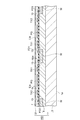
- FIG. 3 is a diagram showing a cross-sectional configuration along the line III-III in FIG.
- FIG. 4 is a diagram showing a cross-sectional configuration along the line IV-IV in FIG.
- FIG. 5 is a diagram showing a cross-sectional configuration along the line VV in FIG.
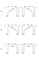
- FIG. 6 is a diagram showing a potential distribution in the vicinity of the second main surface of the semiconductor substrate.
- FIG. 7 is a diagram showing a potential distribution in the vicinity of the second main surface of the semiconductor substrate.
- FIG. 8 is a diagram showing a potential distribution in the vicinity of the second main surface of the semiconductor substrate.
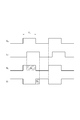
- FIG. 9 is a timing chart of various signals.
- FIG. 10 is a cross-sectional view of the entire imaging device.
- FIG. 11 is a timing chart of various signals.
- FIG. 12 is a diagram illustrating an overall configuration of the distance image measurement device.
- FIG. 13 is a diagram for explaining charge leakage in a conventional distance image sensor.
- FIG. 14 is a schematic plan view showing pixels constituting an imaging region of a distance image sensor according to a modification.
- FIG. 1 is a configuration diagram of a distance image sensor according to the present embodiment.
- the distance image sensor RS is a line sensor having an array structure in which a plurality of distance sensors P 1 to P N (N is a natural number of 2 or more) are arranged in a one-dimensional direction A.
- Each of the plurality of distance sensors P 1 to P N constitutes one pixel of the distance image sensor RS by one or two or more.
- each of the plurality of distance sensors P 1 to P N constitutes one pixel of the distance image sensor RS.
- FIG. 2 is a schematic plan view showing a part of an imaging region in the distance image sensor of FIG.
- FIG. 3 is a diagram showing a cross-sectional configuration along the line III-III in FIG.
- FIG. 4 is a diagram showing a cross-sectional configuration along the line IV-IV in FIG.
- FIG. 5 is a diagram showing a cross-sectional configuration along the line VV in FIG.
- FIGS. 2 to 5 particularly show two adjacent distance sensors P n and P n + 1 (n is a natural number equal to or less than N ⁇ 1).
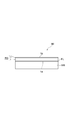
- the distance image sensor RS is a surface incidence type distance image sensor, and includes a semiconductor substrate 1 having first and second main surfaces 1a and 1b facing each other.
- the second main surface 1b is a light incident surface.
- the distance image sensor RS includes a light shielding layer LI in front of the second main surface 1b which is a light incident surface.
- An opening LIa is formed in the one-dimensional direction A in each of the regions corresponding to the plurality of distance sensors P 1 to P N in the light shielding layer LI.
- the opening LIa has a rectangular shape. In the present embodiment, the opening LIa has a rectangular shape.
- the light enters the semiconductor substrate 1 through the opening LIa of the light shielding layer LI. Therefore, the light receiving region is defined in the semiconductor substrate 1 by the opening LIa.
- the light shielding layer LI is made of a metal such as aluminum, for example.
- the semiconductor substrate 1 includes a p-type first semiconductor region 3 which is located on the first principal surface 1a side, p impurity concentration than the first semiconductor region 3 located on the lower and side second main surface 1b - type first Two semiconductor regions 5.
- the semiconductor substrate 1 can be obtained, for example, by growing a p ⁇ type epitaxial layer having an impurity concentration lower than that of the semiconductor substrate on the p type semiconductor substrate.
- an insulating layer 7 is formed on the second main surface 1b (second semiconductor region 5) of the semiconductor substrate 1.
- a plurality of distance sensors P 1 to P N are arranged in the one-dimensional direction A.
- Each of the plurality of distance sensors P 1 to P N includes a photogate electrode PG, a first signal charge storage region FD1, a second signal charge storage region FD2, a third signal charge storage region FD3, and a fourth signal charge storage.
- a region FD4 two first transfer electrodes TX1, two second transfer electrodes TX2, four unnecessary charge collection regions 11a to 11d, four third transfer electrodes TX3, a p-type well region W, It has.
- the conductor 13 (see FIGS. 3 to 5) disposed on the first to fourth signal charge storage regions FD1 to FD4 is omitted.
- the photogate electrode PG is disposed corresponding to the opening LIa.
- the region corresponding to the photogate electrode PG in the semiconductor substrate 1 (second semiconductor region 5) (the region located below the photogate electrode PG in FIGS. 3 to 5) is a charge that generates charges in response to incident light. Functions as a generation area.
- the photogate electrode PG also corresponds to the shape of the opening LIa and has a rectangular shape in plan view.
- the photogate electrode PG has a rectangular shape like the opening LIa. That is, the photogate electrode PG includes first and second long sides L1 and L2 that are orthogonal to the one-dimensional direction A and face each other, and first and second short sides S1 that are parallel to the one-dimensional direction A and face each other. , S2 and a planar shape.
- the photogate electrode PG has a first long side L1 on one side in the one-dimensional direction A and a second long side L2 on the other side in the one-dimensional direction A.
- the first and second signal charge accumulation regions FD1 and FD2 are separated from the photogate electrode PG on the first long side L1 side (one side in the one-dimensional direction A) of the photogate electrode PG and orthogonal to the one-dimensional direction A. They are spaced apart from each other along the direction of the movement.
- the third and fourth signal charge accumulation regions FD3 and FD4 are separated from the photogate electrode PG on the second long side L2 side (the other side in the one-dimensional direction A) of the photogate electrode PG and orthogonal to the one-dimensional direction A. They are spaced apart from each other along the direction of the movement.
- the third signal charge accumulation region FD3 is arranged to face the first signal charge accumulation region FD1 across the photogate electrode PG in the one-dimensional direction A.
- the fourth signal charge accumulation region FD4 is disposed to face the second signal charge accumulation region FD2 with the photogate electrode PG interposed therebetween in the one-dimensional direction A.
- the first to fourth signal charge storage regions FD1 to FD4 are n-type semiconductor regions formed in the second semiconductor region 5 and having a high impurity concentration, and store charges generated in the charge generation region as signal charges.
- the unnecessary charge collection regions 11a and 11b are separated from the photogate electrode PG on the first long side L1 side of the photogate electrode PG and are first and second signal charge accumulation regions along a direction orthogonal to the one-dimensional direction A. They are arranged opposite to each other with FD1 and FD2 interposed therebetween. Along the direction orthogonal to the one-dimensional direction A, the unnecessary charge collection region 11a is adjacent to the first signal charge storage region FD1, and the unnecessary charge collection region 11b is adjacent to the second signal charge storage region FD2.
- the unnecessary charge collection regions 11c and 11d are separated from the photogate electrode PG on the second long side L2 side of the photogate electrode PG, and the third and fourth signal charge accumulation regions along the direction orthogonal to the one-dimensional direction A.
- the FD3 and the FD4 are arranged opposite to each other.
- the unnecessary charge collection region 11c is adjacent to the third signal charge storage region FD3
- the unnecessary charge collection region 11d is adjacent to the fourth signal charge storage region FD4.
- the unnecessary charge collection regions 11a and 11c are arranged to face each other across the photogate electrode PG in the one-dimensional direction A.
- the unnecessary charge collection regions 11b and 11d are arranged to face each other with the photogate electrode PG interposed therebetween in the one-dimensional direction A.
- the unnecessary charge collection regions 11a to 11d are n-type semiconductor regions formed in the second semiconductor region 5 and having a high impurity concentration, and collect the charges generated in the charge generation region as unnecessary charges.
- the well region W surrounds the photogate electrode PG, the first and second transfer electrodes TX1 and TX2, and the first to fourth signal charge storage regions FD1 to FD4 when viewed from the direction orthogonal to the second main surface 1b.
- the second semiconductor region 5 is formed.
- the well region W overlaps with a part of each of the first to fourth signal charge accumulation regions FD1 to FD4 when viewed from the direction orthogonal to the second main surface 1b.
- the outer edge of the well region W substantially coincides with the outer edges of the plurality of distance sensors P 1 to P N.
- the well region W has the same conductivity type as that of the second semiconductor region 5 and has an impurity concentration higher than that of the second semiconductor region 5.
- the well region W suppresses the coupling between the depletion layer expanded by applying a voltage to the photogate electrode PG and the depletion layer expanded from the first to fourth signal charge storage regions FD1 to FD4. Thereby, crosstalk is suppressed.
- the first and second signal charge accumulation regions FD1, FD2 and the unnecessary charge collection regions 11a, 11b are separated from each other along the direction orthogonal to the one-dimensional direction A on the first long side L1 side of the photogate electrode PG.
- the third and fourth signal charge accumulation regions FD3, FD4 and the unnecessary charge collection regions 11c, 11d are separated from each other along the direction orthogonal to the one-dimensional direction A on the second long side L2 side of the photogate electrode PG.
- the first to fourth signal charge accumulation regions FD1 to FD4 and the unnecessary charge collection regions 11a to 11d have a rectangular shape in plan view.
- the first to fourth signal charge accumulation regions FD1 to FD4 and the unnecessary charge collection regions 11a to 11d have a square shape in plan view, and have the same shape.
- One of the distance sensor P n and the distance sensor P n + 1 is arranged at an even number, and the other is arranged at an odd number. That is, in the distance image sensor RS, the distance sensor P n and the distance sensor P n + 1 are alternately arranged in the one-dimensional direction A.
- the distance sensor P n and the distance sensor P n + 1 are arranged in the arrangement order of the first to fourth signal charge accumulation areas FD1 to FD4 and the unnecessary charge collection areas 11a to 11d, and the arrangement order of the first to third transfer electrodes TX1 to TX3. Differ only in the differences. That is, on the first long side L1 side of the photogate electrode PG, the distance sensor Pn includes an unnecessary charge collection region 11a, a first signal charge storage region FD1, a second signal charge storage region FD2, and an unnecessary charge collection region 11b.
- the distance sensor P n + 1 is arranged in this order from the first short side S1 side, whereas the distance sensor P n + 1 is arranged in this order from the second short side S2 side.
- the unnecessary charge collection region 11c, the third signal charge storage region FD3, the fourth signal charge storage region FD4, and the unnecessary charge collection region 11d are arranged in this order.
- the distance sensor P n + 1 is arranged from the one short side S1 side, it is arranged from the second short side S2 side in this order.
- the third transfer electrode TX3, the first transfer electrode TX1, the second transfer electrode TX2, and the third transfer electrode TX3 are in this order in the first short side.
- the distance sensor P n + 1 is arranged from the side S1 side, it is arranged from the second short side S2 side in this order.
- the third transfer electrode TX3, the second transfer electrode TX2, the first transfer electrode TX1, and the third transfer electrode TX3 are in this order in the first short side S1.
- the distance sensor P n + 1 is arranged in this order from the second short side S2 side.
- the distance between the sensor P n fourth signal charge storage region FD4 a distance sensor P n + 1 of the first signal charge accumulating region FD1 of are adjacent in one-dimensional direction A.
- Distance sensor P n of the third signal charge storage region FD3 a distance sensor P n + 1 of the second signal charge accumulating region FD2 are adjacent in the one-dimensional direction A.
- the first signal charge accumulation region FD1 and the fourth signal charge accumulation region FD4 are in the one-dimensional direction.
- the second signal charge storage region FD2 and the third signal charge storage region FD3 are adjacent to each other in the one-dimensional direction A.
- the impurity concentration is high means, for example, that the impurity concentration is about 1 ⁇ 10 17 cm ⁇ 3 or more, and “+” is attached to the conductivity type.
- impurity concentration is low means, for example, about 10 ⁇ 10 15 cm ⁇ 3 or less, and “ ⁇ ” is attached to the conductivity type.
- the thickness / impurity concentration of each semiconductor region is as follows.
- First semiconductor region 3 thickness 10 to 1000 ⁇ m / impurity concentration 1 ⁇ 10 12 to 10 19 cm ⁇ 3
- Second semiconductor region 5 thickness 1 to 50 ⁇ m / impurity concentration 1 ⁇ 10 12 to 10 15 cm ⁇ 3
- First to fourth signal charge accumulation regions FD1 to FD4, unnecessary charge collection regions 11a to 11d thickness 0.1 to 1 ⁇ m / impurity concentration 1 ⁇ 10 18 to 10 20 cm ⁇ 3
- Well region W thickness 0.5 to 5 ⁇ m / impurity concentration 1 ⁇ 10 16 to 10 18 cm ⁇ 3
- the semiconductor substrate 1 (first and second semiconductor regions 3 and 5) is supplied with a reference potential such as a ground potential via a back gate or a through electrode.
- the first transfer electrode TX1 is disposed on the insulating layer 7 and between the first and fourth signal charge storage regions FD1, FD4 and the photogate electrode PG.
- the first transfer electrode TX1 is disposed away from the first and fourth signal charge storage regions FD1, FD4 and the photogate electrode PG.
- the first transfer electrode TX1 causes charges generated in the charge generation region in response to the first transfer signal S 1 (see FIG. 9) to flow into the first and fourth signal charge storage regions FD1 and FD4 as signal charges.
- the second transfer electrode TX2 is disposed on the insulating layer 7 and between the second and third signal charge storage regions FD2, FD3 and the photogate electrode PG.
- the second transfer electrode TX2 is disposed away from the second and third signal charge storage regions FD2, FD3 and the photogate electrode PG.
- the second transfer electrode TX2 uses the charge generated in the charge generation region in response to the second transfer signal S 2 (see FIG. 9) having a phase different from that of the first transfer signal S 1 as the signal charge. It flows into the accumulation areas FD2, FD3.
- the third transfer electrode TX3 is disposed on the insulating layer 7 and between the unnecessary charge collection regions 11a to 11d and the photogate electrode PG.
- the third transfer electrode TX3 is disposed away from the unnecessary charge collection regions 11a to 11d and the photogate electrode PG.
- the third transfer electrode TX3 uses the charge generated in the charge generation region according to the third transfer signal S 3 (see FIG. 9) having a phase different from that of the first transfer signal S 1 and the second transfer signal S 2 as an unnecessary charge. Unnecessary charge collection regions 11a to 11d are caused to flow.
- the first to third transfer electrodes TX1 to TX3 are spaced apart from each other along the direction orthogonal to the one-dimensional direction A on the first long side L1 side and the second long side L2 side of the photogate electrode PG. Yes.
- the first to third transfer electrodes TX1 to TX3 have a rectangular shape in plan view.
- the first to third transfer electrodes TX1 to TX3 have a rectangular shape having a long side in a direction orthogonal to the one-dimensional direction A, and have the same shape.
- the lengths of the long sides of the first to third transfer electrodes TX1 to TX3 are substantially equal to, for example, the length obtained by dividing the first long side L1 of the photogate electrode PG into four equal parts.
- the insulating layer 7 is provided with a contact hole for exposing the surface of the second semiconductor region 5.
- a conductor 13 for connecting the first to fourth signal charge accumulation regions FD1 to FD4 and the unnecessary charge collection regions 11a to 11d to the outside is disposed in the contact hole.
- the semiconductor substrate is made of Si
- the insulating layer 7 is made of SiO 2
- photo gate electrode PG and the first to third transfer electrodes TX1-TX3 is made of polysilicon, these other materials may be used.
- the second transfer signal S 2 of the phase applied to the first transfer signals S 1 and the phase of the second transfer electrode TX2 applied to the first transfer electrode TX1, are 180 degrees.
- Light incident on each of the plurality of distance sensors P 1 to P N is converted into electric charges in the semiconductor substrate 1 (second semiconductor region 5).
- a part of the charges generated in this way is a first transfer electrode according to a potential gradient formed by a voltage applied to the photogate electrode PG and the first and second transfer electrodes TX1, TX2 as a signal charge. It runs in the direction of TX1 or the second transfer electrode TX2, that is, the direction parallel to the first and second short sides S1, S2 of the photogate electrode PG.
- An n-type semiconductor includes a positively ionized donor, has a positive potential, and attracts electrons.
- a part of the charges generated by the incidence of light on each of the plurality of distance sensors P 1 to P N is formed as a potential by a voltage applied to the photogate electrode PG and the third transfer electrode TX3 as unnecessary charges. It travels in the direction of the third transfer electrode TX3 according to the gradient.
- the potential below the third transfer electrode TX3 is greater than the potential of the semiconductor substrate 1 (second semiconductor region 5) below the photogate electrode PG relative to electrons.
- the negative charge (electrons) is pulled down in the direction of the third transfer electrode TX3 and collected in the potential well formed by the unnecessary charge collection regions 11a to 11d.
- a potential (for example, ground potential) lower than the positive potential is applied to the third transfer electrode TX3, a potential barrier is generated by the third transfer electrode TX3, and the charge generated in the semiconductor substrate 1 It is not drawn into 11d.
- FIG. 6 is a diagram showing a potential distribution in the vicinity of the second main surface of the semiconductor substrate along the line III-III in FIG.
- FIG. 7 is a diagram showing a potential distribution in the vicinity of the second main surface of the semiconductor substrate along the line IV-IV in FIG.
- FIG. 8 is a diagram showing a potential distribution in the vicinity of the second main surface of the semiconductor substrate along the line VV in FIG. 6 to 8, the downward direction is the positive direction of the potential.
- FIGS. 6A, 6B, 7A, 7B, and 8A are diagrams for explaining a signal charge accumulation operation.
- FIG. 6C, FIG. 7C, and FIG. 8B are diagrams for explaining an unnecessary charge discharging operation.
- the potential ⁇ PG in the region immediately below the photogate electrode PG is the potential ( ⁇ TX1 , ⁇ TX2 , ⁇ TX3 ) in the region immediately below the adjacent first to third transfer electrodes TX1 to TX3 when no bias is applied. Is set higher than this reference potential.
- the potential ⁇ PG of the charge generation region is higher than the potentials ⁇ TX1 , ⁇ TX2 , and ⁇ TX3 , and the potential distribution has a shape recessed downward in the drawing in the charge generation region.
- the first transfer electrode TX1 When the first transfer signals S 1 of phase applied to the first transfer electrode TX1 is 0 degrees, the first transfer electrode TX1 is given positive potential.
- the second transfer electrode TX2 is supplied with a reverse-phase potential, that is, a potential having a phase of 180 degrees (for example, a ground potential).
- a potential between the potential applied to the first transfer electrode TX1 and the potential applied to the second transfer electrode TX2 is applied to the photogate electrode PG.
- the negative charge e generated in the charge generation region is caused by the potential ⁇ TX1 of the semiconductor immediately below the first transfer electrode TX1 being the potential of the charge generation region. by falls below phi PG, it flows into the first signal charge storage region FD1 and the potential well of the fourth signal charge storage region FD4.
- the second transfer electrode TX2 semiconductor potential phi TX2 immediately below is not lowered, the second signal charge accumulation region FD2 and the potential well of the third signal charge storage region FD3, charge does not flow into.
- signal charges are collected and accumulated in the potential wells of the first signal charge accumulation region FD1 and the fourth signal charge accumulation region FD4.
- the potential is recessed in the positive direction because the n-type impurity is added.
- a potential between the potential applied to the first transfer electrode TX1 and the potential applied to the second transfer electrode TX2 is applied to the photogate electrode PG.
- the negative charge e generated in the charge generation region is caused by the potential ⁇ TX2 of the semiconductor immediately below the second transfer electrode TX2 being the potential of the charge generation region. by falls below phi PG, it flows into the second signal charge storage region FD2 and the potential well of the third signal charge storage region FD3.
- the semiconductor potential phi TX1 directly under the first transfer electrode TX1 is not lowered, the first signal charge accumulation region FD1 and the potential well of the fourth signal charge storage region FD4, charge does not flow into.
- signal charges are collected and accumulated in the potential wells of the second signal charge accumulation region FD2 and the third signal charge accumulation region FD3.
- signal charges are collected and accumulated in the potential wells of the first to fourth signal charge accumulation regions FD1 to FD4.
- the signal charges accumulated in the potential wells of the first to fourth signal charge accumulation regions FD1 to FD4 are read out to the outside.
- a ground potential is applied to the first and second transfer electrodes TX1, TX2. For this reason, as shown in FIGS. 6C and 7C, the potentials ⁇ TX1 and ⁇ TX2 of the semiconductor immediately below the first and second transfer electrodes TX1 and TX2 are not lowered, and the first to fourth signals Charges do not flow into the potential wells of the charge storage regions FD1 to FD4. On the other hand, a positive potential is applied to the third transfer electrode TX3. In this case, as shown in FIG.
- the semiconductor potential phi TX3 immediately below the third transfer electrodes TX3 drops below the potential phi PG charge generation region
- unnecessary charges are collected in the potential wells of the unnecessary charge collection regions 11a to 11d.
- Unnecessary charges collected in the potential wells of the unnecessary charge collection regions 11a to 11d are discharged to the outside. That is, the unnecessary charge collection regions 11a to 11d also function as unnecessary charge discharge regions (unnecessary charge discharge drains).
- the unnecessary charge collection regions 11a to 11d are connected to a fixed potential, for example.
- FIG. 9 is a timing chart of various signals.
- Intensity signal L P and the second transfer signal S 2 of overlapping portions to be applied to the second transfer electrode TX2 of the reflected light is the sum of the second and third signal charge storage region FD2, respectively accumulated amount of charges to FD3 It corresponds to the amount of charge Q 2 is.
- FIG. 10 is a cross-sectional view of the entire imaging device.
- the imaging device IM includes a distance image sensor RS and a wiring board WB.
- the distance image sensor RS is affixed to the wiring substrate WB via the adhesion region FL in a state where the first main surface 1a side of the semiconductor substrate 1 is opposed to the wiring substrate WB.
- the adhesion region FL has an insulating adhesive or filler.
- FIG. 11 is a timing chart of various actual signals.
- the one-frame period TF includes a signal charge accumulation period (accumulation period) T acc and a signal charge read period (readout period) Tro . Focusing on one pixel, in the accumulation period T acc , a drive signal SD having a plurality of pulses is applied to the light source LS (see FIG. 12), and in synchronization therewith, the first and second transfer signals S 1 , S 2 is applied to the first and second transfer electrodes TX1, TX2 in opposite phases. Prior to the distance measurement, the reset signal reset is applied to the first to fourth signal charge accumulation regions FD1 to FD4, and the charges accumulated inside are discharged to the outside.
- accumulation period T acc Focusing on one pixel, in the accumulation period T acc , a drive signal SD having a plurality of pulses is applied to the light source LS (see FIG. 12), and in synchronization therewith, the first and second transfer signals S 1 , S 2 is applied to the first and second transfer electrodes TX1, TX2 in opposite phases. Prior to the
- the signal charges accumulated in the first to fourth signal charge accumulation regions FD1 to FD4 are read.
- the third transfer signal S 3 is ON applied to the third transfer electrodes TX3, a positive potential is applied to the third transfer electrodes TX3, unnecessary charges in the potential wells of the unnecessary charge collection region 11a ⁇ 11d Collected.
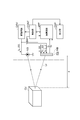
- FIG. 12 is a diagram showing an overall configuration of the distance image measuring apparatus.
- the distance d to the object OJ is measured by a distance image measuring device.
- the light source LS such as a laser beam irradiation apparatus and the LED drive signal S D is applied
- the charge generation region of the intensity signal L P is the range image sensor RS of the reflecting light image reflected by the object OJ Is incident on.
- the amount of electric charge collected in synchronization with the first and second transfer signals S 1, S 2 Q 1, Q 2 are output in synchronization with the drive signal S D calculation Input to circuit ART.
- the distance d is calculated for each pixel as described above, and the calculation result is transferred to the control unit CONT.
- the control unit CONT controls the drive circuit DRV that drives the light source LS, outputs the first to third transfer signals S 1 to S 3 , and displays the calculation result input from the calculation circuit ART on the display DSP. .
- the operation and effect of the distance image sensor RS configured as described above will be described.
- the operation and effect of the distance image sensor RS will be described in comparison with a conventional distance image sensor.
- FIG. 13 is a diagram for explaining charge leakage in a conventional distance image sensor.
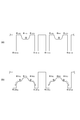
- each of the plurality of distance sensors R 1 to R N arranged in the one-dimensional direction includes the first signal charge accumulation region FD1 and the first transfer electrode on one side in the one-dimensional direction of the photogate electrode PG.
- TX1 is provided, and the second signal charge storage region FD2 and the second transfer electrode TX2 are provided on the other side in the one-dimensional direction of the photogate electrode PG. That is, the plurality of distance sensors R 1 to R N are arranged one-dimensionally in the charge distribution direction. In the two adjacent distance sensors R n and R n + 1 , the first signal charge accumulation region FD1 and the second signal charge accumulation region FD2 are adjacent in a one-dimensional direction.
- the conventional distance image sensor further includes a p-type well region W.
- the well region W surrounds the photogate electrode PG, the first and second transfer electrodes TX1 and TX2, and the first and second signal charge storage regions FD1 and FD2 when viewed from the direction orthogonal to the second main surface 1b.
- the second semiconductor region 5 is formed.
- the well region W overlaps with a part of each of the first and second signal charge storage regions FD1, FD2 when viewed from the direction orthogonal to the second main surface 1b.
- the outer edge of the well region W substantially coincides with the outer edges of the plurality of distance sensors R 1 to R N.
- the first signal charge accumulation region FD1 is disposed on the distance sensor R n side, and the second signal charge accumulation region FD2 is disposed on the opposite side to the distance sensor R n . Therefore, if the distance sensor R n distance sensor R n + 1 to the charge leaks, leakage amount B% to the first signal charge storage region FD1, from leakage amount A% to the second signal charge storage region FD2 also grows.
- the distance sensor R n + 1 light is incident, the distance sensor if R n + 1 distance sensor R n charge leaks from the distance sensor R n, the distance sensor R n + 1 side second signal charge accumulating region FD2 Therefore, the leakage amount D% into the second signal charge storage region FD2 is larger than the leakage amount C% into the first signal charge storage region FD1.
- the distance to be measured should become distance sensor R n and the distance sensor R n + 1 and the same.
- charges leak into each other in the distance sensors R n and R n + 1 so that the amount of charge accumulated in each of the first and second signal charge accumulation regions FD1 and FD2 is equal to the distance sensor R n and the distance. It differs from sensor R n + 1 . Therefore, the distance to be measured may be different between the distance sensor R n and the distance sensor R n + 1.
- a plurality of distance sensors P 1 to P N are arranged in the one-dimensional direction A, and each of the plurality of distance sensors P 1 to P N is a photogate electrode PG.
- the first and second signal charge accumulation regions FD1 and FD2 are provided on one side in the one-dimensional direction A, and the third and fourth signal charge accumulation regions FD3 and FD4 are provided on the other side of the photogate electrode PG.
- the first and fourth signal charge storage regions FD1, FD4 accumulates the signal charges flowing in response to the first transfer signal S 1.
- Second and third signal charge storage region FD2, FD3 accumulates the signal charges flowing in response to the second transfer signal S 2.
- the first and fourth signal charge accumulation regions FD1 and FD4 that accumulate the signal charge that flows in response to the first transfer signal S 1 are primary charge generation regions. together are arranged on each sides of the original direction a, the second transfer signal second and third signal charge storage region FD2, FD3 accumulates the inflow signal charges in response to S 2 is one-dimensional direction of the charge generation region It is arranged on each side of A. For this reason, in each of the plurality of distance sensors P 1 to P N , the charge leaking from the other distance sensors is the first and fourth signal charge accumulations that accumulate the signal charge that flows in accordance with the first transfer signal S 1.
- FD1 a region FD1, FD4, and the second transfer signal second and third signal charge storage region FD2, FD3 accumulates the inflow signal charges in response to S 2, balance is well distributed. Therefore, the influence of charge crosstalk on distance measurement is the same between distance sensors adjacent in the one-dimensional direction A.
- the distance image sensor RS includes unnecessary charge collection regions 11a to 11d that collect charges generated in the charge generation region as unnecessary charges, and a third transfer signal S having a phase different from that of the first and second transfer signals S 1 and S 2. And a third transfer electrode TX3 that allows the charge generated in the charge generation region to flow into the unnecessary charge collection regions 11a to 11d as an unnecessary charge. For this reason, unnecessary charges can be discharged to the outside, so that the distance measurement accuracy can be improved.
- the first and second transfer electrodes TX1 and TX2 are arranged to face each other across the photogate electrode PG in the one-dimensional direction A. That is, in each of the plurality of distance sensors P 1 to P N , the first and second transfer electrodes TX1 and TX2 are arranged without deviation in the direction orthogonal to the one-dimensional direction A. For this reason, even if light is incident only on a portion in the direction orthogonal to the one-dimensional direction A of the photogate electrode PG, and the amount of charge generated in the charge generation region is biased in the direction orthogonal to the one-dimensional direction A, The amount of charge distributed to the first and second transfer electrodes TX1 and TX2 is not easily biased. As a result, the accuracy of the measurement distance is improved.
- the present invention is not limited to the above embodiment.
- the unnecessary charge collection regions 11a to 11d and the third transfer electrode TX3 are disposed on the first long side L1 side or the second long side L2 side of the photogate electrode PG. I can't.
- FIG. 14 is a schematic plan view showing pixels constituting an imaging region of a distance image sensor according to a modification.
- the distance image sensor RS according to the modification includes a plurality of distance sensors P 1 to P N that collect unnecessary charges on the first long side L1 side and the second long side L2 side.
- the regions 11a to 11d one unnecessary charge collecting region 11e, 11f arranged on the first short side S1 side and the second short side S2 side, and the first long side L1 side and the second long side are provided.
- the embodiment includes two third transfer electrodes TX3 arranged on the first short side S1 side and the second short side S2 side instead of the four third transfer electrodes TX3 arranged on the side L2 side. This is mainly different from the distance image sensor RS according to FIG.
- the unnecessary charge collection region 11e is arranged on the first short side S1 side of the photogate electrode PG and is separated from the photogate electrode PG.
- the unnecessary charge collection region 11f is arranged on the second short side S2 side of the photogate electrode PG and spaced from the photogate electrode PG. That is, the unnecessary charge collection regions 11e and 11f are arranged so as to sandwich the photogate electrode PG in a direction orthogonal to the one-dimensional direction A and to be separated from the photogate electrode PG.
- the unnecessary charge collection regions 11e and 11f have a rectangular shape in plan view. Here, it has a rectangular shape, has the same shape, and has long sides parallel to the one-dimensional direction A.
- the first to fourth signal charge accumulation regions FD1 to FD4 have a rectangular shape in plan view, have the same shape, and have long sides parallel to the direction orthogonal to the one-dimensional direction A.
- the third transfer electrode TX3 is disposed between the unnecessary charge collection regions 11e and 11f and the photogate electrode PG, respectively.
- the third transfer electrode TX3 is disposed away from the unnecessary charge collection regions 11e and 11f and the photogate electrode PG.
- the third transfer electrode TX3 has a rectangular shape in plan view, and has the same shape and long sides parallel to the one-dimensional direction A.
- the length of this long side is equal to the length of the first and second short sides S1, S2 of the photogate electrode PG, for example.
- the lengths of the long sides of the first and second transfer electrodes TX1, TX2 are approximately equal to, for example, the lengths of the first and second long sides L1, L2 of the photogate electrode PG divided into two equal parts, respectively.
- the unnecessary charge collection regions 11a to 11d and the third transfer electrode TX3 are arranged on the first long side L1 side and the second long side L2 side of the photogate electrode PG, and in addition, the first short side of the photogate electrode PG is arranged. Unnecessary charge collection regions 11e and 11f and a third transfer electrode TX3 may be further arranged on the side S1 side or the second short side S2 side.
- the number of unnecessary charge collection regions is not limited to four or two and can be set as appropriate, and need not be provided.
- the unnecessary charge collection region may be arranged, for example, between the first and second transfer electrodes TX1 and TX2, and may be appropriately arranged.
- the distance image sensor RS is a line sensor in which each of the plurality of distance sensors P 1 to P N is arranged one-dimensionally, but may be arranged two-dimensionally. In this case, a two-dimensional image can be easily obtained. A two-dimensional image can also be obtained by rotating the line sensor or by scanning with two line sensors.
- the distance image sensor RS is not limited to the surface incident type distance image sensor.
- the distance image sensor RS may be a back-illuminated distance image sensor.
- the charge generation region in which charge is generated in response to incident light may be configured by a photodiode (for example, an embedded photodiode).
- the p-type and n-type conductivity types in the distance image sensor RS according to the present embodiment may be switched so as to be opposite to those described above.
- the present invention can be used for a charge distribution type distance image sensor.
- 11a to 11f Unnecessary charge collection region, A: One-dimensional direction, FD1: First signal charge storage region, FD2: Second signal charge storage region, FD3 ... Third signal charge storage region, FD4 ... Fourth signal charge storage region , P 1 to P N ... distance sensor, PG ... photogate electrode, RS ... distance image sensor, S 1 ... first transfer signal, S 2 ... second transfer signal, S 3 ... third transfer signal, TX1 ... first Transfer electrode, TX2 ... second transfer electrode, TX3 ... third transfer electrode.
Landscapes
- Engineering & Computer Science (AREA)
- Physics & Mathematics (AREA)
- Computer Networks & Wireless Communication (AREA)
- General Physics & Mathematics (AREA)
- Radar, Positioning & Navigation (AREA)
- Remote Sensing (AREA)
- Electromagnetism (AREA)
- Solid State Image Pick-Up Elements (AREA)
- Optical Radar Systems And Details Thereof (AREA)
- Measurement Of Optical Distance (AREA)
- Transforming Light Signals Into Electric Signals (AREA)
Abstract
Description
第一半導体領域3:厚さ10~1000μm/不純物濃度1×1012~1019cm-3
第二半導体領域5:厚さ1~50μm/不純物濃度1×1012~1015cm-3
第一~第四信号電荷蓄積領域FD1~FD4、不要電荷収集領域11a~11d:厚さ0.1~1μm/不純物濃度1×1018~1020cm-3
ウェル領域W:厚さ0.5~5μm/不純物濃度1×1016~1018cm-3
Claims (3)
- 複数の距離センサが一次元方向に配置されている距離画像センサであって、
前記複数の距離センサそれぞれは、
入射光に応じて電荷が発生する電荷発生領域と、
前記電荷発生領域の前記一次元方向の一方側に前記電荷発生領域から離間し且つ前記一次元方向と直交する方向に沿って互いに離間して配置され、前記電荷発生領域にて発生した電荷を信号電荷として蓄積する前記第一及び第二信号電荷蓄積領域と、
前記電荷発生領域の前記一次元方向の他方側に前記電荷発生領域から離間し且つ前記一次元方向で前記電荷発生領域を挟んで前記第一信号電荷蓄積領域と対向して配置され、前記電荷発生領域にて発生した電荷を信号電荷として蓄積する第三信号電荷蓄積領域と、
前記電荷発生領域の前記一次元方向の他方側に前記電荷発生領域から離間し且つ前記一次元方向で前記電荷発生領域を挟んで前記第二信号電荷蓄積領域と対向して配置され、前記電荷発生領域にて発生した電荷を信号電荷として蓄積する第四信号電荷蓄積領域と、
前記第一及び第四信号電荷蓄積領域と前記電荷発生領域との間にそれぞれ配置され、第一転送信号に応じて前記電荷発生領域にて発生した電荷を信号電荷として前記第一及び第四信号電荷蓄積領域に流入させる二つの第一転送電極と、
前記第二及び第三信号電荷蓄積領域と前記電荷発生領域との間にそれぞれ配置され、前記第一転送信号と位相が異なる第二転送信号に応じて前記電荷発生領域にて発生した電荷を信号電荷として前記第二及び前記第三信号電荷蓄積領域に流入させる二つの第二転送電極と、を備えており、
前記一次元方向に隣り合ういずれの二つの前記距離センサにおいて、前記第一信号電荷蓄積領域と前記第四信号電荷蓄積領域とが前記一次元方向で隣り合うと共に、前記第二信号電荷蓄積領域と前記第三信号電荷蓄積領域とが前記一次元方向で隣り合っている、距離画像センサ。 - 前記電荷発生領域の前記一次元方向の一方側及び他方側に前記電荷発生領域から離間して配置され、前記電荷発生領域にて発生した電荷を不要電荷として収集する複数の不要電荷収集領域と、
前記複数の不要電荷収集領域と前記電荷発生領域との間にそれぞれ配置され、前記第一及び第二転送信号と位相が異なる第三転送信号に応じて前記電荷発生領域にて発生した電荷を不要電荷として前記複数の不要電荷収集領域に流入させる複数の第三転送電極と、を更に備えている、請求項1に記載の距離画像センサ。 - 前記一次元方向と直交する方向で前記電荷発生領域を挟み且つ前記電荷発生領域から離間して配置され、前記電荷発生領域にて発生した電荷を不要電荷として収集する複数の不要電荷収集領域と、
前記複数の不要電荷収集領域と前記電荷発生領域との間にそれぞれ配置され、前記第一及び第二転送信号と位相が異なる第三転送信号に応じて前記電荷発生領域にて発生した電荷を不要電荷として前記複数の不要電荷収集領域に流入させる複数の第三転送電極と、を更に備えている、請求項1に記載の距離画像センサ。
Priority Applications (5)
| Application Number | Priority Date | Filing Date | Title |
|---|---|---|---|
| KR1020167027500A KR102232213B1 (ko) | 2014-04-18 | 2015-04-17 | 거리 화상 센서 |
| CH01354/16A CH711151B8 (de) | 2014-04-18 | 2015-04-17 | Entfernungsabbildungssensor. |
| US15/302,178 US10436908B2 (en) | 2014-04-18 | 2015-04-17 | Range image sensor |
| DE112015001877.8T DE112015001877T5 (de) | 2014-04-18 | 2015-04-17 | Entfernungsabbildungssensor |
| CN201580020107.5A CN106233157B (zh) | 2014-04-18 | 2015-04-17 | 距离图像传感器 |
Applications Claiming Priority (2)
| Application Number | Priority Date | Filing Date | Title |
|---|---|---|---|
| JP2014-086175 | 2014-04-18 | ||
| JP2014086175A JP6315679B2 (ja) | 2014-04-18 | 2014-04-18 | 距離画像センサ |
Publications (1)
| Publication Number | Publication Date |
|---|---|
| WO2015159977A1 true WO2015159977A1 (ja) | 2015-10-22 |
Family
ID=54324178
Family Applications (1)
| Application Number | Title | Priority Date | Filing Date |
|---|---|---|---|
| PCT/JP2015/061876 Ceased WO2015159977A1 (ja) | 2014-04-18 | 2015-04-17 | 距離画像センサ |
Country Status (7)
| Country | Link |
|---|---|
| US (1) | US10436908B2 (ja) |
| JP (1) | JP6315679B2 (ja) |
| KR (1) | KR102232213B1 (ja) |
| CN (1) | CN106233157B (ja) |
| CH (1) | CH711151B8 (ja) |
| DE (1) | DE112015001877T5 (ja) |
| WO (1) | WO2015159977A1 (ja) |
Families Citing this family (5)
| Publication number | Priority date | Publication date | Assignee | Title |
|---|---|---|---|---|
| KR102615195B1 (ko) | 2018-07-19 | 2023-12-18 | 삼성전자주식회사 | ToF 기반의 3D 이미지 센서 및 그 이미지 센서를 구비한 전자 장치 |
| JP2020113573A (ja) * | 2019-01-08 | 2020-07-27 | キヤノン株式会社 | 光電変換装置 |
| US20230027464A1 (en) * | 2019-12-26 | 2023-01-26 | Hamamatsu Photonics K.K. | Distance measurement device, and method for driving distance measurement sensor |
| DE112020006361T5 (de) * | 2019-12-26 | 2022-10-27 | Hamamatsu Photonics K.K. | Lichtdetektionsvorrichtung und Verfahren zum Betreiben von Photosensor |
| CN114339084B (zh) * | 2020-09-30 | 2025-04-25 | 思特威(上海)电子科技股份有限公司 | Tof图像传感器像素结构及测距系统 |
Citations (3)
| Publication number | Priority date | Publication date | Assignee | Title |
|---|---|---|---|---|
| JP2007526448A (ja) * | 2003-06-17 | 2007-09-13 | カネスタ インコーポレイテッド | 三次元及び色彩検出における電荷管理のための方法及び装置 |
| JP2011112376A (ja) * | 2009-11-24 | 2011-06-09 | Hamamatsu Photonics Kk | 距離センサ及び距離画像センサ |
| JP2011133464A (ja) * | 2009-11-24 | 2011-07-07 | Hamamatsu Photonics Kk | 距離センサ及び距離画像センサ |
Family Cites Families (13)
| Publication number | Priority date | Publication date | Assignee | Title |
|---|---|---|---|---|
| JPS582999B2 (ja) | 1977-10-20 | 1983-01-19 | 株式会社関口 | 節水型洗剤 |
| WO2002049366A1 (en) * | 2000-12-14 | 2002-06-20 | 3Dv Systems, Ltd. | 3d camera |
| JP3906859B2 (ja) | 2004-09-17 | 2007-04-18 | 松下電工株式会社 | 距離画像センサ |
| JP5153062B2 (ja) | 2005-07-13 | 2013-02-27 | 新光電気工業株式会社 | 固体酸化物型燃料電池 |
| US7781811B2 (en) * | 2005-08-30 | 2010-08-24 | National University Corporation Shizuoka University | Semiconductor range-finding element and solid-state imaging device |
| JP2008122223A (ja) * | 2006-11-13 | 2008-05-29 | Suzuki Motor Corp | 距離計測装置 |
| JP5528739B2 (ja) | 2009-08-12 | 2014-06-25 | 株式会社ジャパンディスプレイ | 検出装置、表示装置、および物体の近接距離測定方法 |
| JP5244076B2 (ja) * | 2009-11-24 | 2013-07-24 | 浜松ホトニクス株式会社 | 距離センサ及び距離画像センサ |
| JP5460304B2 (ja) | 2009-12-24 | 2014-04-02 | 株式会社第一興商 | パーソナルマイクに対応するカラオケ装置 |
| JP2012083213A (ja) * | 2010-10-12 | 2012-04-26 | Hamamatsu Photonics Kk | 距離センサ及び距離画像センサ |
| JP5518667B2 (ja) | 2010-10-12 | 2014-06-11 | 浜松ホトニクス株式会社 | 距離センサ及び距離画像センサ |
| US8520114B2 (en) | 2011-06-01 | 2013-08-27 | Global Oled Technology Llc | Apparatus for displaying and sensing images |
| US9229096B2 (en) * | 2011-07-27 | 2016-01-05 | Semiconductor Components Industries, Llc | Time-of-flight imaging systems |
-
2014
- 2014-04-18 JP JP2014086175A patent/JP6315679B2/ja active Active
-
2015
- 2015-04-17 CH CH01354/16A patent/CH711151B8/de unknown
- 2015-04-17 KR KR1020167027500A patent/KR102232213B1/ko active Active
- 2015-04-17 US US15/302,178 patent/US10436908B2/en active Active
- 2015-04-17 DE DE112015001877.8T patent/DE112015001877T5/de active Pending
- 2015-04-17 WO PCT/JP2015/061876 patent/WO2015159977A1/ja not_active Ceased
- 2015-04-17 CN CN201580020107.5A patent/CN106233157B/zh active Active
Patent Citations (3)
| Publication number | Priority date | Publication date | Assignee | Title |
|---|---|---|---|---|
| JP2007526448A (ja) * | 2003-06-17 | 2007-09-13 | カネスタ インコーポレイテッド | 三次元及び色彩検出における電荷管理のための方法及び装置 |
| JP2011112376A (ja) * | 2009-11-24 | 2011-06-09 | Hamamatsu Photonics Kk | 距離センサ及び距離画像センサ |
| JP2011133464A (ja) * | 2009-11-24 | 2011-07-07 | Hamamatsu Photonics Kk | 距離センサ及び距離画像センサ |
Also Published As
| Publication number | Publication date |
|---|---|
| JP6315679B2 (ja) | 2018-04-25 |
| CN106233157B (zh) | 2018-08-28 |
| KR102232213B1 (ko) | 2021-03-24 |
| US10436908B2 (en) | 2019-10-08 |
| KR20160144988A (ko) | 2016-12-19 |
| DE112015001877T5 (de) | 2017-01-12 |
| CH711151B1 (de) | 2017-10-13 |
| US20170031025A1 (en) | 2017-02-02 |
| JP2015206634A (ja) | 2015-11-19 |
| CH711151B8 (de) | 2017-12-15 |
| CN106233157A (zh) | 2016-12-14 |
Similar Documents
| Publication | Publication Date | Title |
|---|---|---|
| JP6231940B2 (ja) | 測距装置及び測距装置の駆動方法 | |
| JP5558999B2 (ja) | 距離センサ及び距離画像センサ | |
| JP5244076B2 (ja) | 距離センサ及び距離画像センサ | |
| CN103155150B (zh) | 距离传感器以及距离图像传感器 | |
| JP5620087B2 (ja) | 距離センサ及び距離画像センサ | |
| JP6386777B2 (ja) | 距離画像センサ | |
| JP6315679B2 (ja) | 距離画像センサ | |
| JP6010425B2 (ja) | 距離センサ及び距離画像センサ | |
| JP5502694B2 (ja) | 距離センサ及び距離画像センサ | |
| JP2012083221A (ja) | 距離センサ及び距離画像センサ | |
| JP2012083214A (ja) | 距離センサ及び距離画像センサ | |
| JP2012083220A (ja) | 距離センサ及び距離画像センサ | |
| JP2012083219A (ja) | 距離センサ及び距離画像センサ | |
| JP2012083222A (ja) | 距離センサ及び距離画像センサ |
Legal Events
| Date | Code | Title | Description |
|---|---|---|---|
| 121 | Ep: the epo has been informed by wipo that ep was designated in this application |
Ref document number: 15779607 Country of ref document: EP Kind code of ref document: A1 |
|
| ENP | Entry into the national phase |
Ref document number: 20167027500 Country of ref document: KR Kind code of ref document: A |
|
| WWE | Wipo information: entry into national phase |
Ref document number: 15302178 Country of ref document: US |
|
| WWE | Wipo information: entry into national phase |
Ref document number: 10201600001354 Country of ref document: CH |
|
| WWE | Wipo information: entry into national phase |
Ref document number: 112015001877 Country of ref document: DE |
|
| 122 | Ep: pct application non-entry in european phase |
Ref document number: 15779607 Country of ref document: EP Kind code of ref document: A1 |