WO2015159328A1 - 薄膜トランジスタ基板の製造方法 - Google Patents
薄膜トランジスタ基板の製造方法 Download PDFInfo
- Publication number
- WO2015159328A1 WO2015159328A1 PCT/JP2014/006377 JP2014006377W WO2015159328A1 WO 2015159328 A1 WO2015159328 A1 WO 2015159328A1 JP 2014006377 W JP2014006377 W JP 2014006377W WO 2015159328 A1 WO2015159328 A1 WO 2015159328A1
- Authority
- WO
- WIPO (PCT)
- Prior art keywords
- film
- cumn alloy
- alloy film
- cumn
- thin film
- Prior art date
- Legal status (The legal status is an assumption and is not a legal conclusion. Google has not performed a legal analysis and makes no representation as to the accuracy of the status listed.)
- Ceased
Links
Images










Classifications
-
- H—ELECTRICITY
- H10—SEMICONDUCTOR DEVICES; ELECTRIC SOLID-STATE DEVICES NOT OTHERWISE PROVIDED FOR
- H10P—GENERIC PROCESSES OR APPARATUS FOR THE MANUFACTURE OR TREATMENT OF DEVICES COVERED BY CLASS H10
- H10P74/00—Testing or measuring during manufacture or treatment of wafers, substrates or devices
- H10P74/23—Testing or measuring during manufacture or treatment of wafers, substrates or devices characterised by multiple measurements, corrections, marking or sorting processes
-
- G—PHYSICS
- G09—EDUCATION; CRYPTOGRAPHY; DISPLAY; ADVERTISING; SEALS
- G09F—DISPLAYING; ADVERTISING; SIGNS; LABELS OR NAME-PLATES; SEALS
- G09F9/00—Indicating arrangements for variable information in which the information is built-up on a support by selection or combination of individual elements
- G09F9/30—Indicating arrangements for variable information in which the information is built-up on a support by selection or combination of individual elements in which the desired character or characters are formed by combining individual elements
-
- H—ELECTRICITY
- H10—SEMICONDUCTOR DEVICES; ELECTRIC SOLID-STATE DEVICES NOT OTHERWISE PROVIDED FOR
- H10D—INORGANIC ELECTRIC SEMICONDUCTOR DEVICES
- H10D30/00—Field-effect transistors [FET]
- H10D30/60—Insulated-gate field-effect transistors [IGFET]
- H10D30/67—Thin-film transistors [TFT]
-
- H—ELECTRICITY
- H10—SEMICONDUCTOR DEVICES; ELECTRIC SOLID-STATE DEVICES NOT OTHERWISE PROVIDED FOR
- H10D—INORGANIC ELECTRIC SEMICONDUCTOR DEVICES
- H10D30/00—Field-effect transistors [FET]
- H10D30/60—Insulated-gate field-effect transistors [IGFET]
- H10D30/67—Thin-film transistors [TFT]
- H10D30/6729—Thin-film transistors [TFT] characterised by the electrodes
-
- H—ELECTRICITY
- H10—SEMICONDUCTOR DEVICES; ELECTRIC SOLID-STATE DEVICES NOT OTHERWISE PROVIDED FOR
- H10D—INORGANIC ELECTRIC SEMICONDUCTOR DEVICES
- H10D30/00—Field-effect transistors [FET]
- H10D30/60—Insulated-gate field-effect transistors [IGFET]
- H10D30/67—Thin-film transistors [TFT]
- H10D30/674—Thin-film transistors [TFT] characterised by the active materials
- H10D30/6755—Oxide semiconductors, e.g. zinc oxide, copper aluminium oxide or cadmium stannate
-
- H—ELECTRICITY
- H10—SEMICONDUCTOR DEVICES; ELECTRIC SOLID-STATE DEVICES NOT OTHERWISE PROVIDED FOR
- H10D—INORGANIC ELECTRIC SEMICONDUCTOR DEVICES
- H10D64/00—Electrodes of devices having potential barriers
- H10D64/01—Manufacture or treatment
- H10D64/011—Manufacture or treatment of electrodes ohmically coupled to a semiconductor
-
- H—ELECTRICITY
- H10—SEMICONDUCTOR DEVICES; ELECTRIC SOLID-STATE DEVICES NOT OTHERWISE PROVIDED FOR
- H10D—INORGANIC ELECTRIC SEMICONDUCTOR DEVICES
- H10D64/00—Electrodes of devices having potential barriers
- H10D64/60—Electrodes characterised by their materials
- H10D64/62—Electrodes ohmically coupled to a semiconductor
-
- H—ELECTRICITY
- H10—SEMICONDUCTOR DEVICES; ELECTRIC SOLID-STATE DEVICES NOT OTHERWISE PROVIDED FOR
- H10D—INORGANIC ELECTRIC SEMICONDUCTOR DEVICES
- H10D86/00—Integrated devices formed in or on insulating or conducting substrates, e.g. formed in silicon-on-insulator [SOI] substrates or on stainless steel or glass substrates
- H10D86/40—Integrated devices formed in or on insulating or conducting substrates, e.g. formed in silicon-on-insulator [SOI] substrates or on stainless steel or glass substrates characterised by multiple TFTs
- H10D86/441—Interconnections, e.g. scanning lines
-
- H—ELECTRICITY
- H10—SEMICONDUCTOR DEVICES; ELECTRIC SOLID-STATE DEVICES NOT OTHERWISE PROVIDED FOR
- H10D—INORGANIC ELECTRIC SEMICONDUCTOR DEVICES
- H10D86/00—Integrated devices formed in or on insulating or conducting substrates, e.g. formed in silicon-on-insulator [SOI] substrates or on stainless steel or glass substrates
- H10D86/40—Integrated devices formed in or on insulating or conducting substrates, e.g. formed in silicon-on-insulator [SOI] substrates or on stainless steel or glass substrates characterised by multiple TFTs
- H10D86/60—Integrated devices formed in or on insulating or conducting substrates, e.g. formed in silicon-on-insulator [SOI] substrates or on stainless steel or glass substrates characterised by multiple TFTs wherein the TFTs are in active matrices
-
- H—ELECTRICITY
- H10—SEMICONDUCTOR DEVICES; ELECTRIC SOLID-STATE DEVICES NOT OTHERWISE PROVIDED FOR
- H10D—INORGANIC ELECTRIC SEMICONDUCTOR DEVICES
- H10D99/00—Subject matter not provided for in other groups of this subclass
-
- H—ELECTRICITY
- H10—SEMICONDUCTOR DEVICES; ELECTRIC SOLID-STATE DEVICES NOT OTHERWISE PROVIDED FOR
- H10P—GENERIC PROCESSES OR APPARATUS FOR THE MANUFACTURE OR TREATMENT OF DEVICES COVERED BY CLASS H10
- H10P70/00—Cleaning of wafers, substrates or parts of devices
- H10P70/20—Cleaning during device manufacture
- H10P70/27—Cleaning during device manufacture during, before or after processing of conductive materials, e.g. polysilicon or amorphous silicon layers
-
- H—ELECTRICITY
- H10—SEMICONDUCTOR DEVICES; ELECTRIC SOLID-STATE DEVICES NOT OTHERWISE PROVIDED FOR
- H10P—GENERIC PROCESSES OR APPARATUS FOR THE MANUFACTURE OR TREATMENT OF DEVICES COVERED BY CLASS H10
- H10P74/00—Testing or measuring during manufacture or treatment of wafers, substrates or devices
- H10P74/20—Testing or measuring during manufacture or treatment of wafers, substrates or devices characterised by the properties tested or measured, e.g. structural or electrical properties
- H10P74/203—Structural properties, e.g. testing or measuring thicknesses, line widths, warpage, bond strengths or physical defects
Definitions
- the present disclosure relates to a method for manufacturing a thin film transistor substrate.
- An active matrix display device such as a liquid crystal display device or an organic EL display device uses a TFT substrate on which a thin film transistor (TFT) is formed as a switching element or a driving element.
- TFT thin film transistor
- Patent Document 1 discloses an active matrix organic EL display device using a TFT substrate.
- the configuration of the TFT includes a bottom gate TFT having a structure in which a gate electrode is formed below the channel layer (substrate side), or a top gate TFT having a structure in which the gate electrode is formed above the channel layer. is there.
- a silicon semiconductor or an oxide semiconductor is used for the channel layer of the TFT.
- a plurality of wirings for transmitting signals (voltages) for driving each pixel are formed on a TFT substrate (TFT array substrate) including a plurality of pixels arranged in a matrix.
- the wiring of the TFT substrate has become longer and the wiring resistance has increased due to the increase in the size of the substrate accompanying the increase in the screen size of the display device. For this reason, it is desired to reduce the resistance of the wiring.
- the wiring is formed in the same layer using the same material as the source / drain electrodes in the TFT. For this reason, the source / drain electrodes are required to have not only the performance as a TFT but also the performance as a wiring.
- wirings and electrodes covered with an insulating film are electrically connected to other electrodes and wirings through contact holes formed in the insulating film.
- an insulating film interlayer insulating film
- a contact hole is formed in the insulating film on the CuMn alloy film to expose the surface of the CuMn alloy film.
- the contact resistance is generated on the CuMn alloy film by exposing the surface of the CuMn alloy film, the contact resistance cannot be controlled so far, and it is difficult to realize a TFT substrate having a desired performance. There is.
- the technique disclosed herein aims to obtain a TFT substrate having a desired performance.
- one aspect of a method of manufacturing a thin film transistor substrate is a method of manufacturing a thin film transistor substrate including a thin film transistor having a CuMn alloy film, the step of forming the CuMn alloy film, And a control step of controlling contact resistance on the surface of the CuMn alloy film based on the contact angle of the surface.
- a TFT substrate having desired performance can be realized.
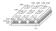
- FIG. 1 is a partially cutaway perspective view of an organic EL display device according to an embodiment.
- FIG. 2 is a perspective view illustrating an example of a pixel bank of the organic EL display device according to the embodiment.
- FIG. 3 is an electric circuit diagram showing a configuration of a pixel circuit in the organic EL display device according to the embodiment.
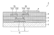
- FIG. 4 is a schematic cross-sectional view of the TFT substrate according to the embodiment.
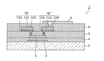
- FIG. 5 is a schematic cross-sectional view of a TFT substrate according to another embodiment.
- FIG. 6 is a diagram showing the relationship between the CuMn surface exposure time and the contact resistance in the CuMn alloy film and the ITO film.
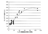
- FIG. 7 is a diagram showing the relationship between the CuMn surface exposure time in the CuMn alloy film and the ITO film and the contact angle of the surface of the CuMn alloy film.
- FIG. 8 is a diagram showing an analysis result of peak separation of Cu2p3 / 2 spectrum by XPS in a CuMn alloy film.
- FIG. 9A is a diagram showing a change in the abundance ratio of CuO with respect to the standing time.
- FIG. 9B is a diagram showing a change in the abundance ratio of metalCu or Cu 2 O with respect to the standing time.
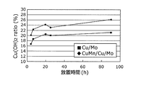
- FIG. 9C is a diagram showing a change in the abundance ratio of Cu (OH) 2 with respect to the standing time.
- FIG. 10 is a diagram showing the relationship between the contact angle on the surface of the CuMn alloy film and the contact resistance on the surface of the CuMn alloy film.
- FIG. 11A is a cross-sectional view of the step of forming a gate electrode (first wiring layer) in the TFT substrate manufacturing method according to the embodiment.
- FIG. 11B is a cross-sectional view of the first insulating film (gate insulating film) forming step in the manufacturing method of the TFT substrate according to the embodiment.
- FIG. 11C is a cross-sectional view of the oxide semiconductor layer forming step in the manufacturing method of the TFT substrate according to the exemplary embodiment.
- FIG. 11D is a cross-sectional view of the second insulating film forming step in the manufacturing method of the TFT substrate according to the embodiment.
- FIG. 11E is a cross-sectional view of the contact hole forming step in the manufacturing method of the TFT substrate according to the exemplary embodiment.
- FIG. 11F is a cross-sectional view of the source / drain electrode layer (second wiring layer) forming step in the manufacturing method of the TFT substrate according to the embodiment.
- FIG. 11G is a cross-sectional view of the third insulating film forming step in the manufacturing method of the TFT substrate according to the embodiment.
- FIG. 11H is a cross-sectional view of a resist film forming step in the TFT substrate manufacturing method according to the embodiment.
- FIG. 11I is a cross-sectional view of the resist film patterning forming step in the TFT substrate manufacturing method according to the embodiment.
- FIG. 11J is a cross-sectional view of the contact hole forming step in the manufacturing method of the TFT substrate according to the embodiment.
- FIG. 11K is a cross-sectional view of the resist film removing step in the manufacturing method of the TFT substrate according to the embodiment.
- FIG. 11L is a cross-sectional view of the contact angle measurement step in the method for manufacturing a TFT substrate according to the embodiment.
- FIG. 11M is a cross-sectional view of the third wiring layer forming step in the manufacturing method of the TFT substrate according to the embodiment.
- FIG. 12 is a schematic cross-sectional view of a TFT substrate according to a modification.
- FIG. 1 is a partially cutaway perspective view of an organic EL display device according to an embodiment.
- FIG. 2 is a perspective view illustrating an example of a pixel bank of the organic EL display device according to the embodiment.
- an organic EL display device 100 includes a TFT substrate (TFT array substrate) 1 on which a plurality of thin film transistors are arranged, an anode 131 that is a lower electrode, and an EL layer 132 that is a light emitting layer made of an organic material. And a laminated structure with an organic EL element (light emitting part) 130 including a cathode 133 which is a transparent upper electrode.
- the organic EL display device 100 in this embodiment is a top emission type, and the anode 131 is a reflective electrode.
- the organic EL display device 100 is not limited to the top emission type, and may be a bottom emission type.
- the TFT substrate 1 has a plurality of pixels 110 arranged in a matrix, and each pixel 110 is provided with a pixel circuit 120.
- the organic EL element 130 is formed corresponding to each of the plurality of pixels 110, and the light emission of each organic EL element 130 is controlled by the pixel circuit 120 provided in each pixel 110.
- the organic EL element 130 is formed on an interlayer insulating film (planarization layer) formed so as to cover a plurality of thin film transistors.
- the organic EL element 130 has a configuration in which an EL layer 132 is disposed between the anode 131 and the cathode 133.
- a hole transport layer is further stacked between the anode 131 and the EL layer 132, and an electron transport layer is further stacked between the EL layer 132 and the cathode 133.
- another organic functional layer may be provided between the anode 131 and the cathode 133.
- Each pixel 110 is driven and controlled by the respective pixel circuit 120.
- Source wiring (signal wiring) 150 and a plurality of power supply wirings (not shown in FIG. 1) arranged in parallel with the source wiring 150 are formed.
- Each pixel 110 is partitioned by, for example, an orthogonal gate wiring 140 and a source wiring 150.
- the gate wiring 140 is connected to the gate electrode of the thin film transistor operating as a switching element included in each pixel circuit 120 for each row.
- the source wiring 150 is connected to the source electrode of the thin film transistor that operates as a switching element included in each pixel circuit 120 for each column.
- the power supply wiring is connected to the drain electrode of the thin film transistor operating as a driving element included in each pixel circuit 120 for each column.
- each pixel 110 of the organic EL display device 100 is configured by sub-pixels 110R, 110G, and 110B of three colors (red, green, and blue), and these sub-pixels 110R, 110G, and 110B. Are formed in a matrix on the display surface.
- the sub-pixels 110R, 110G, and 110B are separated from each other by the bank 111.
- the banks 111 are formed in a lattice shape so that the ridges extending in parallel to the gate wiring 140 and the ridges extending in parallel to the source wiring 150 intersect each other.
- Each of the portions surrounded by the protrusions (that is, the opening of the bank 111) and the sub-pixels 110R, 110G, and 110B have a one-to-one correspondence.
- the bank 111 is a pixel bank, but may be a line bank.
- the anode 131 is formed for each of the sub-pixels 110R, 110G, and 110B on the interlayer insulating film (flattening layer) on the TFT substrate 1 and in the opening of the bank 111.
- the EL layer 132 is formed for each of the sub-pixels 110R, 110G, and 110B on the anode 131 and in the opening of the bank 111.
- the transparent cathode 133 is continuously formed on the plurality of banks 111 so as to cover all the EL layers 132 (all the subpixels 110R, 110G, and 110B).
- the pixel circuit 120 is provided for each of the sub-pixels 110R, 110G, and 110B, and each of the sub-pixels 110R, 110G, and 110B and the corresponding pixel circuit 120 are electrically connected by a contact hole and a relay electrode.
- the sub-pixels 110R, 110G, and 110B have the same configuration except that the emission color of the EL layer 132 is different.
- FIG. 3 is an electric circuit diagram showing a configuration of a pixel circuit in the organic EL display device according to the embodiment.
- the pixel circuit 120 includes a thin film transistor SwTr that operates as a switching element, a thin film transistor DrTr that operates as a driving element, and a capacitor C that stores data to be displayed on the corresponding pixel 110.
- the thin film transistor SwTr is a switching transistor for selecting the pixel 110
- the thin film transistor DrTr is a drive transistor for driving the organic EL element 130.
- the thin film transistor SwTr includes a gate electrode G1 connected to the gate wiring 140, a source electrode S1 connected to the source wiring 150, a drain electrode D1 connected to the capacitor C and the gate electrode G2 of the thin film transistor DrTr, and a semiconductor film (FIG. Not shown).
- a predetermined voltage is applied to the connected gate wiring 140 and source wiring 150
- the voltage applied to the source wiring 150 is stored in the capacitor C as a data voltage.
- the thin film transistor DrTr includes a gate electrode G2 connected to the drain electrode D1 of the thin film transistor SwTr and the capacitor C, a drain electrode D2 connected to the power supply wiring 160 and the capacitor C, and a source electrode connected to the anode 131 of the organic EL element 130. It is comprised by S2 and a semiconductor film (not shown).
- the thin film transistor DrTr supplies a current corresponding to the data voltage held by the capacitor C from the power supply wiring 160 to the anode 131 of the organic EL element 130 through the source electrode S2. Thereby, in the organic EL element 130, a drive current flows from the anode 131 to the cathode 133, and the EL layer 132 emits light.
- the organic EL display device 100 having the above configuration employs an active matrix system in which display control is performed for each pixel 110 located at the intersection of the gate wiring 140 and the source wiring 150. Thereby, the corresponding organic EL element 130 selectively emits light by the thin film transistors SwTr and DrTr of each pixel 110 (each sub-pixel 110R, 110G, 110B), and a desired image is displayed.
- FIG. 4 is a schematic cross-sectional view of the TFT substrate according to the embodiment.
- the TFT substrate 1 in the organic EL display device 100 will be described.
- the thin film transistor Tr in this embodiment can be applied to both the thin film transistor SwTr (switching transistor) and the thin film transistor DrTr (drive transistor).
- the TFT substrate 1 includes a substrate 2, a gate electrode 3, a gate insulating film 4 (first insulating film), an oxide semiconductor layer 5, and an insulating layer 6 (second insulating film). , Source electrode 7S and drain electrode 7D, insulating layer 8 (third insulating film), and upper wiring 9.
- the gate electrode 3, the source electrode 7S and the drain electrode 7D, and the upper layer wiring 9 are made of a metal material, and the layer in which these electrodes and wiring are formed is a metal layer (wiring layer). Specifically, the layer in which the gate electrode 3 is formed is a first wiring layer (first metal layer), and the layer in which the source electrode 7S and the drain electrode 7D are formed is a second wiring layer (second metal layer). The layer on which the upper wiring 9 is formed is a third wiring layer (third metal layer).
- the TFT substrate 1 in the present embodiment has a three-layer wiring layer structure, and each metal layer can be used as a wiring layer for forming various wirings. That is, by patterning a metal film (conductive film) formed on each metal layer into a predetermined shape, a desired wiring or electrode having a predetermined shape can be formed in addition to the electrodes and wirings described above.
- a metal film conductive film
- a desired wiring or electrode having a predetermined shape can be formed in addition to the electrodes and wirings described above.
- a gate wiring 140, a source wiring 150, and a power wiring 160 shown in FIG. 1 are formed. Also, contact holes are formed in the insulating layer between the upper and lower metal layers in order to connect the wirings of the respective metal layers or connect the wirings and the electrodes.
- the thin film transistor Tr is composed of a gate electrode 3, a gate insulating film 4, an oxide semiconductor layer 5, a source electrode 7S, and a drain electrode 7D.
- the gate electrode 3, the source electrode 7S, and the drain electrode 7D correspond to the gate electrode G2, the source electrode S2, and the drain electrode D2 in FIG. 3, respectively.
- the thin film transistor Tr in this embodiment is a bottom-gate TFT.
- the substrate 2 is, for example, a glass substrate such as a G8 substrate. Further, as the substrate 2, a flexible substrate such as a resin substrate may be used. An undercoat layer may be formed on the surface of the substrate 2.
- the gate electrode 3 is formed in a predetermined shape above the substrate 2.
- the gate electrode 3 include metals such as titanium (Ti), molybdenum (Mo), tungsten (W), aluminum (Al), gold (Au), copper (Cu), or ITO (Indium Tin Oxide).
- a conductive oxide such as indium tin) is used.
- an alloy such as molybdenum tungsten (MoW) can also be used as the gate electrode 3.
- Ti, Al, Au, or the like is used as a metal having good adhesion to the oxide, and a laminate sandwiching these metals can be used as the gate electrode 3. .
- the gate insulating film 4 is formed between the gate electrode 3 and the oxide semiconductor layer 5.
- the gate insulating film 4 is formed on the substrate 2 so as to cover the gate electrode 3.
- an oxide thin film such as a silicon oxide film or a hafnium oxide film, a nitride film such as a silicon nitride film or a single layer film of a silicon oxynitride film, or a laminated film thereof is used.
- the oxide semiconductor layer 5 is formed in a predetermined shape above the substrate 2.
- the oxide semiconductor layer 5 is a channel layer (semiconductor layer) of the thin film transistor Tr and is formed to face the gate electrode 3.
- the oxide semiconductor layer 5 is formed in an island shape on the gate insulating film 4 above the gate electrode 3.
- the oxide semiconductor layer 5 is preferably composed of a transparent amorphous oxide semiconductor (TAOS) such as InGaZnO x (IGZO) containing In—Ga—Zn—O.
- TAOS transparent amorphous oxide semiconductor
- IGZO InGaZnO x
- a thin film transistor using a transparent amorphous oxide semiconductor as a channel layer has high carrier mobility and is suitable for a large-screen and high-definition display device. Further, since the transparent amorphous oxide semiconductor can be formed at a low temperature, it can be easily formed over a flexible substrate.
- the amorphous oxide semiconductor of InGaZnO X can be formed by a vapor phase film forming method such as a sputtering method or a laser vapor deposition method using, for example, a polycrystalline sintered body having an InGaO 3 (ZnO) 4 composition.
- the insulating layer 6 is formed on the gate insulating film 4 so as to cover the oxide semiconductor layer 5. That is, the oxide semiconductor layer 5 is covered with the insulating layer 6, and the insulating layer 6 functions as a protective layer (channel protective layer) that protects the oxide semiconductor layer 5.
- the insulating layer 6 is, for example, a single layer film of an oxide film such as a silicon oxide film (SiO 2 ) or an aluminum oxide film (Al 2 O 3 ), or a laminated film of these oxide films. A part of the insulating layer 6 is opened so as to penetrate, and the oxide semiconductor layer 5 is connected to the source electrode 7S and the drain electrode 7D through the opening (contact hole).
- the source electrode 7S and the drain electrode 7D are formed on the insulating layer 6 in a predetermined shape. Specifically, the source electrode 7S and the drain electrode 7D are connected to the oxide semiconductor layer 5 through contact holes provided in the insulating layer 6, and have a predetermined interval in the substrate horizontal direction on the insulating layer 6. They are arranged opposite each other.
- the source electrode 7S and the drain electrode 7D both contain copper (Cu) as a main component, and have a laminated structure of a copper film (Cu film) and a copper manganese alloy film (CuMn alloy film).
- the source electrode 7S is a stacked film in which a first film 71S that is a Cu film and a second film 72S that is a CuMn alloy film are stacked in this order from the bottom to the top.
- the drain electrode 7D is a stacked film in which a first film 71D that is a Cu film and a second film 72D that is a CuMn alloy film are stacked in this order from the bottom to the top.
- the first films 71S and 71D, which are Cu films, are preferably thicker than the second films 72S and 72D.
- the resistance of the source electrode 7S and the drain electrode 7D can be reduced, and the wiring formed in the second metal layer (Wiring in the same layer as the source electrode 7S and the drain electrode 7D) can be a low resistance wiring.
- the CuMn alloy film as the uppermost layer (cap layer) of the source electrode 7S and the drain electrode 7D, it is possible to suppress the Cu film from being oxidized and the Cu film from being altered. Thereby, the increase in resistance of the source electrode 7S and the drain electrode 7D due to oxidation of Cu can be suppressed.
- the CuMn alloy film means an alloy film of copper and manganese.
- the insulating layer 8 is formed on the insulating layer 6 so as to cover the source electrode 7S and the drain electrode 7D.
- the insulating layer 8 is, for example, a single layer film of an oxide film such as a silicon oxide film (SiO 2 ) or an aluminum oxide film (Al 2 O 3 ), or a laminated film of these oxide films.
- the upper wiring 9 is made of a conductive film formed in a predetermined shape on the insulating layer 8, and is connected to the drain electrode 7D through a contact hole formed in the insulating layer 8.
- the upper wiring 9 in the present embodiment is an ITO film made of ITO.
- the TFT substrate 1 in the present embodiment is configured as described above.
- the source electrode 7S and the drain electrode 7D have a two-layer structure of a CuMn alloy film and a Cu film, but the present invention is not limited to this.
- a TFT substrate 1 ' having a source electrode 7S' and a drain electrode 7D 'having a three-layer structure may be used.
- the source electrode 7S ′ is formed by stacking a third film 73S that is a Mo (molybdenum) film or a CuMn film, a first film 71S that is a Cu film, and a second film 72S that is a CuMn alloy film. It may be a film.
- the drain electrode 7D ′ may be a laminated film of a third film 73D that is a Mo film or a CuMn film, a first film 71D that is a Cu film, and a second film 72D that is a CuMn alloy film. .
- the CuMn film or the Mo film as the lowermost layer of the source electrode 7S ′ and the drain electrode 7D ′, it is possible to suppress the diffusion of Cu atoms to the lower layer in the second film (Cu film) and It is possible to improve the adhesion.
- the TFT substrate when wiring and electrodes between different wiring layers are physically connected, a contact hole is formed in the insulating film (interlayer insulating film). At this time, when the ITO film in the upper wiring layer is formed on the CuMn alloy film in the lower wiring layer through the contact hole of the insulating film, the surface of the CuMn alloy film is exposed.
- the TFT substrate 1 shown in FIG. 4 when connecting the second film 72D (CuMn alloy film) of the drain electrode 7D and the upper wiring 9 (ITO film), after forming a contact hole in the insulating layer 8, The surface of the second film 72D is exposed.
- the contact between the ITO film and the CuMn alloy film increases with an increase in the waiting time from the exposure of the CuMn alloy film (second film 72D) to the covering with the ITO film (upper wiring 9). Resistance increases. As a result, display uniformity and reliability of the display panel are reduced.
- the change in contact resistance is because the exposed surface of the CuMn alloy film is oxidized during the standby time until the ITO film is formed.
- a method of observing the change in contact resistance as an in-line process could not be controlled. For this reason, it has been difficult to realize a TFT substrate having desired performance.
- FIG. 6 is a diagram showing the relationship between the CuMn surface exposure time and the contact resistance in the CuMn alloy film and the ITO film.
- the contact resistance increases as the CuMn surface exposure time increases, and the CuMn surface exposure time is constant as described above. It was found that the contact resistance hardly changed after the time (about 60 hours) was exceeded.
- the CuMn surface exposure time is the time after removing the resist film in forming the contact hole in the insulating film (insulating layer 8) covering the CuMn alloy film.
- the contact resistance is measured after forming an ITO film on the CuMn alloy film.
- the contact resistance of the second film 72D (CuMn alloy film) of each drain electrode 7D of the plurality of thin film transistors Tr on the TFT substrate 1 shown in FIG. 4 is measured by a contact chain.
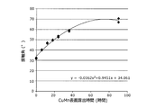
- FIG. 7 is a diagram showing the relationship between the CuMn surface exposure time in the CuMn alloy film and the ITO film and the contact angle of the surface of the CuMn alloy film.
- the contact angle increases as the CuMn surface exposure time increases, and the CuMn surface exposure time is constant time. After exceeding (about 60 hours), it was found that the contact angle hardly changed.
- the contact angle is a contact angle with respect to water and was measured using a contact angle meter.
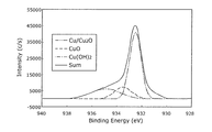
- the inventor also analyzed the atomic bonding state (composition change), not the surface state (contact angle), of the CuMn alloy film. This point will be described with reference to FIGS. 8 and 9A to 9C.
- FIG. 8 is a diagram showing an analysis result of peak separation of Cu2p3 / 2 spectrum by XPS in a CuMn alloy film.
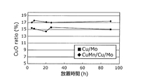
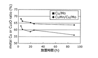
- FIGS. 9A to 9C The results are shown in FIGS. 9A to 9C.
- FIG. 9A is a diagram showing a change in the abundance ratio of CuO with respect to the standing time.
- FIG. 9B is a diagram showing a change in the abundance ratio of metalCu or Cu 2 O with respect to the standing time.
- FIG. 9C is a diagram showing a change in the abundance ratio of Cu (OH) 2 with respect to the standing time.
- the standing time in FIGS. 9A to 9C is the CuMn surface exposure time described above, and the process of leaving the atmosphere after removing the resist film when the contact hole is formed in the insulating film covering the CuMn alloy film. It's time.
- FIG. 10 is a diagram showing the relationship between the contact angle on the surface of the CuMn alloy film and the contact resistance on the surface of the CuMn alloy film.
- the present invention has been made on the basis of a new finding that has not existed in the past that there is a correlation between the contact angle on the surface of the CuMn alloy film and the contact resistance on the surface of the CuMn alloy film.
- the inventors have found that the contact resistance on the surface of the CuMn alloy film can be controlled by monitoring the contact angle of the surface of the CuMn alloy film.
- the contact angle of the surface of the CuMn alloy film is measured, and the correlation between the contact angle of the CuMn alloy film and the contact resistance on the surface of the CuMn alloy film, which has been measured and calculated as reference data in advance (for example, based on FIG. 10), the contact resistance on the surface of the CuMn alloy film is determined by determining whether or not the contact angle of the CuMn alloy film actually measured in the TFT substrate manufacturing process is equal to or less than a predetermined value. Control.
- the contact resistance on the surface of the CuMn alloy film can be controlled as desired by measuring the contact angle of the CuMn alloy film formed on the substrate in-line and feeding it back to the process.
- FIGS. 11A to 11M are cross-sectional views of each step in the method of manufacturing the thin film transistor substrate according to the embodiment.
- the manufacturing method of the TFT substrate 1 in the present embodiment is a manufacturing method of a TFT substrate including a TFT having a CuMn alloy film, and the contact resistance on the surface of the CuMn alloy film based on the contact angle of the surface of the CuMn alloy film.
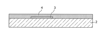
- a substrate 2 is prepared, and a gate electrode 3 having a predetermined shape is formed above the substrate 2.
- a gate metal film is formed on the substrate 2 of a G8 glass substrate by a sputtering method, and the gate metal film is processed using a photolithography method and a wet etching method, thereby forming the gate electrode 3 having a predetermined shape.
- a gate insulating film 4 is formed above the substrate 2.
- the gate insulating film 4 made of silicon oxide is formed by plasma CVD or the like so as to cover the gate electrode 3.
- an oxide semiconductor layer 5 having a predetermined shape is formed above the substrate 2.
- the oxide semiconductor layer 5 is formed over the gate insulating film 4.
- a transparent amorphous oxide semiconductor of InGaZnO X is formed on the gate insulating film 4 by a sputtering method or the like, and the transparent amorphous oxide semiconductor is processed by using a photolithography method and an etching method, so that the upper portion of the gate electrode 3 is formed. Then, an oxide semiconductor layer 5 having a predetermined shape is formed.
- an insulating layer 6 is formed on the gate insulating film 4 so as to cover the oxide semiconductor layer 5.
- the insulating layer 6 made of a silicon oxide film is formed by plasma CVD.
- contact holes CH1 and CH1 ′ for contacting the oxide semiconductor layer 5 with the source electrode 7S and the drain electrode 7D are formed by removing a part of the insulating layer 6.
- the contact holes CH1 and CH1 ' are formed in the insulating layer 6 by using a photolithography method and an etching method so that a part of the oxide semiconductor layer 5 is exposed.
- a source electrode 7S and a drain electrode 7D having a predetermined shape are formed on the insulating layer 6 so as to be connected to the oxide semiconductor layer 5.
- a Cu film is formed on the insulating layer 6 by sputtering so as to fill the contact holes CH1 and CH1 ′ of the insulating layer 6, and then a CuMn alloy film is formed on the Cu film by sputtering. Form a film.
- the laminated film of the Cu film and the CuMn alloy film is processed into a predetermined shape by using a photolithography method and an etching method.
- the CuMn alloy film and the Cu film are patterned by wet etching using hydrogen peroxide as an etchant.
- a drain electrode 7D having a laminated structure with the second film 72D can be formed.
- an insulating layer 8 is formed on the insulating layer 6 so as to cover the source electrode 7S and the drain electrode 7D. That is, the insulating layer 8 is formed on the second films 72S and 72D that are CuMn alloy films.
- the insulating layer 8 made of a silicon oxide film is formed at a film forming temperature of 300 ° C. by plasma CVD.
- an upper wiring 9 having a predetermined shape is formed on the insulating layer 8 so as to be connected to the drain electrode 7D through the contact hole of the insulating layer 8.
- contact holes are formed in the insulating layer 8 to expose the second films 72S and 72D, which are CuMn alloy films.
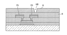
- a resist film R is formed on the insulating layer 8, and then the resist film R is exposed and exposed by photolithography to form a drain electrode as shown in FIG. 11I.
- a through hole HR is formed in the resist film R on 7D.
- a portion corresponding to the through hole HR in the insulating layer 8 is selectively removed by etching to form a contact hole CH2 in the insulating layer 8, and the surface of the drain electrode 7D is exposed.
- the surface of the second film 72D (CuMn alloy film) which is the uppermost layer of the drain electrode 7D is exposed.
- the contact hole CH2 is formed by dry etching, but wet etching may be used.
- the resist film R is removed with a stripping solution such as an alkaline solution.
- control process the contact resistance on the surface of the CuMn alloy film is controlled based on the contact angle of the surface of the CuMn alloy film (control process).
- control step the contact resistance on the surface of the CuMn alloy film is calculated based on the correlation (for example, FIG. 10) between the contact angle on the surface of the CuMn alloy film and the contact resistance on the surface of the CuMn alloy film.
- the control step includes a contact angle measurement step of measuring the contact angle of the surface of the CuMn alloy film and a determination step of determining whether or not the measured contact angle is equal to or less than a predetermined value.
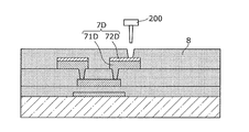
- the contact angle of the surface of the exposed drain electrode 7D is measured using a contact angle meter 200. That is, the contact angle of the surface of the CuMn alloy film that is the uppermost layer film of the drain electrode 7D exposed from the contact hole CH2 of the insulating layer 8 is measured (contact angle measurement step).
- the measured contact angle is a predetermined value or less (determination step). At this time, when it is determined that the measured contact angle exceeds a predetermined value, the surface of the CuMn alloy film is cleaned (cleaning step).
- the surface of the CuMn alloy film can be cleaned using an alkaline solution.
- the same stripping solution as the resist film R can be used as the cleaning solution.
- residues such as the resist film R remaining on the surface of the CuMn alloy film can be removed.
- the contact angle of the surface of the CuMn alloy film can be reduced, and the contact resistance of the CuMn alloy film can be reduced.
- the contact resistance increase curve becomes large. Therefore, the predetermined value of the contact angle in the determination step is 52 °. Good. That is, when the measured contact angle exceeds 52 °, the contact resistance is controlled by cleaning the surface of the CuMn alloy film so that the contact angle is 52 ° or less. As described above, the contact resistance can be easily controlled by determining the threshold value when the contact angle of the CuMn alloy film having a small rising curve is 52 °. That is, in a region where the slope of the contact resistance with respect to the contact angle is steep, the fluctuation range of the contact resistance with respect to the unit contact angle becomes large, and it becomes difficult to control the contact resistance.
- the upper wiring 9 that is an ITO film is formed on the second film 72D that is a CuMn alloy film through the contact hole CH2 of the insulating layer 8.
- an ITO film is formed on the insulating layer 8 by a sputtering method so as to fill the contact hole CH2 of the insulating layer 8, and the ITO film is formed by using a photolithography method and an etching method.
- an upper wiring 9 having a predetermined shape is formed on the insulating layer 8.
- the ITO film is patterned by wet etching using an oxalic acid-based etchant.
- the control process of controlling the contact resistance on the surface of CuMn alloy film based on the contact angle of the surface of CuMn alloy film is included.
- the thin film transistor substrate As described above, the thin film transistor substrate, the method for manufacturing the thin film transistor substrate, and the organic EL display device have been described based on the embodiments. However, the present invention is not limited to the above embodiments.
- the source electrode and the drain electrode are exemplified as the member having the CuMn alloy film on the TFT substrate, but the present invention is not limited thereto.
- a member having a CuMn alloy film such as a TFT substrate 1 ′′ having a four-layer wiring layer structure shown in FIG. 12, may be used as the intermediate wiring 9 ′′.
- the source electrode 7S ′′ and the drain electrode 7D ′′ are Cu films made of pure Cu, and further insulated from the intermediate wiring 9 ′′ (third wiring layer).
- a layer 10 (third insulating layer) and an upper layer wiring 11 (fourth wiring layer) are provided.
- the intermediate wiring 9 ′′ has a laminated structure of a first film 91 that is a Cu film and a second film 92 that is a CuMn alloy film.
- the insulating layer 10 is a resin material such as an acrylic resin, a silicon oxide film, or the like. And is formed on the insulating layer 8 so as to cover the intermediate wiring 9 ′′.
- the upper layer wiring 11 is an ITO film formed in a predetermined shape on the insulating layer 8 and is connected to the drain electrode 7D ′′ via a contact hole formed in the insulating layer 8.
- the contact resistance is the contact resistance between the CuMn alloy film and the ITO film, but is not limited thereto.
- the contact resistance between the CuMn alloy film and the conductive film formed thereon can be controlled by measuring the contact angle on the surface of the CuMn alloy film.
- the CuMn alloy film has a laminated structure with the Cu film, but the present invention is not limited to this.
- the CuMn alloy film may be a single layer wiring or electrode.
- the thin film transistor is a bottom gate type, but may be a top gate type.
- the thin film transistor is a channel etching stopper type (channel protection type), but may be a channel etching type. That is, in the above embodiment, the insulating layer 6 may not be formed.
- an organic EL display device is described as a display device using a thin film transistor substrate.
- the thin film transistor substrate in the above embodiment is used for other display devices using an active matrix substrate such as a liquid crystal display device. Can also be applied.
- the display device such as the organic EL display device described above can be used as a flat panel display and applied to all electronic devices having a display panel such as a television set, a personal computer, and a mobile phone. can do. In particular, it is suitable for a large-screen and high-definition display device.
- the technology disclosed herein can be widely used in a thin film transistor substrate using an oxide semiconductor, a manufacturing method thereof, a display device such as an organic EL display device using the thin film transistor substrate, and the like.
Landscapes
- Physics & Mathematics (AREA)
- General Physics & Mathematics (AREA)
- Engineering & Computer Science (AREA)
- Theoretical Computer Science (AREA)
- Internal Circuitry In Semiconductor Integrated Circuit Devices (AREA)
- Thin Film Transistor (AREA)
- Electrodes Of Semiconductors (AREA)
Abstract
Description
まず、TFT基板が用いられる表示装置の一例として、有機EL表示装置の構成について説明する。
図1は、実施の形態に係る有機EL表示装置の一部切り欠き斜視図である。図2は、実施の形態に係る有機EL表示装置のピクセルバンクの例を示す斜視図である。
次に、実施の形態に係るTFT基板について、図4を用いて説明する。図4は、実施の形態に係るTFT基板の概略断面図である。以下の実施の形態では、上記有機EL表示装置100におけるTFT基板1について説明する。なお、本実施の形態における薄膜トランジスタTrは、上記の薄膜トランジスタSwTr(スイッチングトランジスタ)及び薄膜トランジスタDrTr(駆動トランジスタ)のいずれにも適用することができる。
次に、CuMn合金膜の表面状態や原子結合状態の分析結果について、本発明の知見を得るに至った経緯も含めて詳細に説明する。
次に、上記のコンタクト抵抗の制御を用いた実施の形態に係るTFT基板1の製造方法について、図11A~図11Mを用いて説明する。図11A~図11Mは、実施の形態に係る薄膜トランジスタ基板の製造方法における各工程の断面図である。
以上、薄膜トランジスタ基板、薄膜トランジスタ基板の製造方法及び有機EL表示装置について、実施の形態に基づいて説明したが、本発明は、上記実施の形態に限定されるものではない。
2 基板
3、G1、G2 ゲート電極
4 ゲート絶縁膜
5 酸化物半導体層
6、8、10 絶縁層
7S、7S’、7S”、S1、S2 ソース電極
7D、7D’、7D”、D1、D2 ドレイン電極
9、11 上層配線
9” 中間配線
100 有機EL表示装置
110 画素
110R、110G、110B サブ画素
111 バンク
120 画素回路
130 有機EL素子
131 陽極
132 EL層
133 陰極
140 ゲート配線
150 ソース配線
160 電源配線
200 接触角計
SwTr、DrTr 薄膜トランジスタ
C キャパシタ
CH1、CH1’、CH2、 コンタクトホール
HR 貫通孔
Claims (8)
- CuMn合金膜を有する薄膜トランジスタを備える薄膜トランジスタ基板の製造方法であって、
前記CuMn合金膜を形成する工程と、
前記CuMn合金膜の表面の接触角に基づいて前記CuMn合金膜の表面上のコンタクト抵抗を制御する制御工程とを含む
薄膜トランジスタ基板の製造方法。 - 前記制御工程では、予め算出した、CuMn合金膜の表面の接触角とCuMn合金膜の表面上のコンタクト抵抗との相関関係に基づいて、前記CuMn合金膜の表面上のコンタクト抵抗を制御する
請求項1に記載の薄膜トランジスタ基板の製造方法。 - 前記制御工程は、
前記CuMn合金膜の表面の接触角を測定する接触角測定工程と、
測定した前記接触角が所定の値以下であるか否かを判定する判定工程とを含む
請求項1又は2に記載の薄膜トランジスタ基板の製造方法。 - 前記接触角の所定の値は、52°である
請求項3に記載の薄膜トランジスタ基板の製造方法。 - 前記制御工程は、さらに、前記判定工程において、測定した前記接触角が前記所定の値を超えていると判定された場合に前記CuMn合金膜の表面を洗浄する洗浄工程を含む
請求項3又は4に記載の薄膜トランジスタ基板の製造方法。 - 前記洗浄工程では、アルカリ溶液を用いて前記CuMn合金膜の表面を洗浄する
請求項5に記載の薄膜トランジスタ基板の製造方法。 - さらに、
前記CuMn合金膜上に絶縁層を成膜する工程と、
コンタクトホールを前記絶縁層に形成して前記CuMn合金膜を露出させる工程と、
前記コンタクトホールを介して前記CuMn合金膜上にITO膜を形成する工程とを含み、
前記制御工程は、前記CuMn合金膜を露出させる工程と前記ITO膜を形成する工程との間に行う
請求項1~6のいずれか1項に記載の薄膜トランジスタ基板の製造方法。 - 前記CuMn膜は、前記薄膜トランジスタのソース電極及びドレイン電極の最上層膜である
請求項1~7のいずれか1項に記載の薄膜トランジスタ基板の製造方法。
Priority Applications (2)
| Application Number | Priority Date | Filing Date | Title |
|---|---|---|---|
| JP2016513500A JP6248265B2 (ja) | 2014-04-15 | 2014-12-22 | 薄膜トランジスタ基板の製造方法 |
| US15/304,060 US9824942B2 (en) | 2014-04-15 | 2014-12-22 | Method of manufacturing thin-film transistor substrate including a copper alloy film |
Applications Claiming Priority (2)
| Application Number | Priority Date | Filing Date | Title |
|---|---|---|---|
| JP2014084036 | 2014-04-15 | ||
| JP2014-084036 | 2014-04-15 |
Publications (1)
| Publication Number | Publication Date |
|---|---|
| WO2015159328A1 true WO2015159328A1 (ja) | 2015-10-22 |
Family
ID=54323580
Family Applications (1)
| Application Number | Title | Priority Date | Filing Date |
|---|---|---|---|
| PCT/JP2014/006377 Ceased WO2015159328A1 (ja) | 2014-04-15 | 2014-12-22 | 薄膜トランジスタ基板の製造方法 |
Country Status (3)
| Country | Link |
|---|---|
| US (1) | US9824942B2 (ja) |
| JP (1) | JP6248265B2 (ja) |
| WO (1) | WO2015159328A1 (ja) |
Citations (3)
| Publication number | Priority date | Publication date | Assignee | Title |
|---|---|---|---|---|
| JP2002214177A (ja) * | 2001-01-15 | 2002-07-31 | Toda Constr Co Ltd | 抗菌用材の性能の確認方法、防汚用材の性能の確認方法、抗菌用材の抗菌活性度の評価方法、防汚用材の防汚性能の評価方法と、その用材の表面における菌数の評価方法および用材の表面における汚れの評価方法 |
| JP2004186275A (ja) * | 2002-11-29 | 2004-07-02 | Honda Motor Co Ltd | 電気二重層コンデンサ用の電極シート、その製造方法、分極性電極および分極性電極を用いた電気二重層コンデンサ |
| WO2011089722A1 (ja) * | 2010-01-22 | 2011-07-28 | トヨタ自動車株式会社 | 正極およびその製造方法 |
Family Cites Families (11)
| Publication number | Priority date | Publication date | Assignee | Title |
|---|---|---|---|---|
| JP2000165002A (ja) | 1998-11-26 | 2000-06-16 | Furontekku:Kk | 電子機器用基板及びその製造方法と電子機器 |
| JP2000282033A (ja) | 1999-01-25 | 2000-10-10 | Harufusa Hiuga | 金属表面処理剤及び金属層の表面処理方法 |
| JP2009004518A (ja) * | 2007-06-20 | 2009-01-08 | Kobe Steel Ltd | 薄膜トランジスタ基板、および表示デバイス |
| JP5053956B2 (ja) | 2008-06-20 | 2012-10-24 | キヤノン株式会社 | 有機el表示装置 |
| JP2012027159A (ja) | 2010-07-21 | 2012-02-09 | Kobe Steel Ltd | 表示装置 |
| JP5988564B2 (ja) | 2010-10-27 | 2016-09-07 | 住友化学株式会社 | 有機薄膜トランジスタの製造方法及び該方法で製造された有機薄膜トランジスタ |
| JP5171990B2 (ja) | 2011-05-13 | 2013-03-27 | 株式会社神戸製鋼所 | Cu合金膜および表示装置 |
| KR20120138074A (ko) | 2011-06-14 | 2012-12-24 | 삼성디스플레이 주식회사 | 박막 트랜지스터, 및 박막 트랜지스터 표시판과 이들을 제조하는 방법 |
| JP2013110014A (ja) * | 2011-11-22 | 2013-06-06 | Panasonic Corp | 有機el素子の製造方法および有機el表示パネル |
| JP2015159132A (ja) | 2012-06-14 | 2015-09-03 | パナソニック株式会社 | 薄膜トランジスタ |
| JP2014032999A (ja) * | 2012-08-01 | 2014-02-20 | Panasonic Liquid Crystal Display Co Ltd | 薄膜トランジスタ及びその製造方法 |
-
2014
- 2014-12-22 WO PCT/JP2014/006377 patent/WO2015159328A1/ja not_active Ceased
- 2014-12-22 US US15/304,060 patent/US9824942B2/en active Active
- 2014-12-22 JP JP2016513500A patent/JP6248265B2/ja active Active
Patent Citations (3)
| Publication number | Priority date | Publication date | Assignee | Title |
|---|---|---|---|---|
| JP2002214177A (ja) * | 2001-01-15 | 2002-07-31 | Toda Constr Co Ltd | 抗菌用材の性能の確認方法、防汚用材の性能の確認方法、抗菌用材の抗菌活性度の評価方法、防汚用材の防汚性能の評価方法と、その用材の表面における菌数の評価方法および用材の表面における汚れの評価方法 |
| JP2004186275A (ja) * | 2002-11-29 | 2004-07-02 | Honda Motor Co Ltd | 電気二重層コンデンサ用の電極シート、その製造方法、分極性電極および分極性電極を用いた電気二重層コンデンサ |
| WO2011089722A1 (ja) * | 2010-01-22 | 2011-07-28 | トヨタ自動車株式会社 | 正極およびその製造方法 |
Also Published As
| Publication number | Publication date |
|---|---|
| US20170040234A1 (en) | 2017-02-09 |
| JPWO2015159328A1 (ja) | 2017-04-13 |
| JP6248265B2 (ja) | 2017-12-20 |
| US9824942B2 (en) | 2017-11-21 |
Similar Documents
| Publication | Publication Date | Title |
|---|---|---|
| JP6019329B2 (ja) | 表示装置および電子機器 | |
| KR102248641B1 (ko) | 유기전계 발광소자 | |
| JP6019507B2 (ja) | 薄膜トランジスタ基板及び薄膜トランジスタ基板の製造方法 | |
| US9312279B2 (en) | Thin film transistor array substrate, method of manufacturing the same, and display apparatus including the same | |
| JP5766481B2 (ja) | 表示装置および電子機器 | |
| US20160204126A1 (en) | Thin-film transistor substrate and method for fabricating the same | |
| US9362312B2 (en) | Semiconductor device, display unit, and electronic apparatus | |
| KR20170115641A (ko) | 트랜지스터 표시판, 그 제조 방법 및 이를 포함하는 표시 장치 | |
| JP2010182818A (ja) | 薄膜トランジスタおよび表示装置 | |
| CN111081734B (zh) | 薄膜晶体管元件基板及其制造方法、和有机el显示装置 | |
| JP2021013021A (ja) | ディスプレイ装置 | |
| JP2015149467A (ja) | 薄膜トランジスタ基板の製造方法 | |
| US9627515B2 (en) | Method of manufacturing thin-film transistor substrate | |
| KR20220030492A (ko) | 표시 장치 및 표시 장치의 제조 방법 | |
| US20180233596A1 (en) | Semiconductor device | |
| JP2012204548A (ja) | 表示装置およびその製造方法 | |
| US10847655B2 (en) | Semiconductor device | |
| WO2013187046A1 (ja) | 薄膜トランジスタ | |
| CN111048554A (zh) | 有机发光显示装置 | |
| JP6248265B2 (ja) | 薄膜トランジスタ基板の製造方法 | |
| JP6311900B2 (ja) | 薄膜トランジスタ基板の製造方法 | |
| JP6500202B2 (ja) | 薄膜トランジスタ及び薄膜トランジスタの製造方法 | |
| WO2016067527A1 (ja) | 薄膜トランジスタの製造方法 |
Legal Events
| Date | Code | Title | Description |
|---|---|---|---|
| 121 | Ep: the epo has been informed by wipo that ep was designated in this application |
Ref document number: 14889448 Country of ref document: EP Kind code of ref document: A1 |
|
| ENP | Entry into the national phase |
Ref document number: 2016513500 Country of ref document: JP Kind code of ref document: A |
|
| WWE | Wipo information: entry into national phase |
Ref document number: 15304060 Country of ref document: US |
|
| NENP | Non-entry into the national phase |
Ref country code: DE |
|
| 122 | Ep: pct application non-entry in european phase |
Ref document number: 14889448 Country of ref document: EP Kind code of ref document: A1 |