WO2015156291A1 - 圧力センサ - Google Patents
圧力センサ Download PDFInfo
- Publication number
- WO2015156291A1 WO2015156291A1 PCT/JP2015/060881 JP2015060881W WO2015156291A1 WO 2015156291 A1 WO2015156291 A1 WO 2015156291A1 JP 2015060881 W JP2015060881 W JP 2015060881W WO 2015156291 A1 WO2015156291 A1 WO 2015156291A1
- Authority
- WO
- WIPO (PCT)
- Prior art keywords
- terminal
- pressure sensor
- eprom
- lead pin
- pressure
- Prior art date
- Legal status (The legal status is an assumption and is not a legal conclusion. Google has not performed a legal analysis and makes no representation as to the accuracy of the status listed.)
- Ceased
Links
Images


Classifications
-
- G—PHYSICS
- G01—MEASURING; TESTING
- G01L—MEASURING FORCE, STRESS, TORQUE, WORK, MECHANICAL POWER, MECHANICAL EFFICIENCY, OR FLUID PRESSURE
- G01L9/00—Measuring steady of quasi-steady pressure of fluid or fluent solid material by electric or magnetic pressure-sensitive elements; Transmitting or indicating the displacement of mechanical pressure-sensitive elements, used to measure the steady or quasi-steady pressure of a fluid or fluent solid material, by electric or magnetic means
Definitions
- the present invention relates to a pressure sensor including a pressure detection element having a terminal for writing to EPROM and EPROM, and in particular, information stored in EPROM is erased by high voltage pulse noise applied to the terminal for writing to EPROM.
- the present invention relates to a pressure sensor that can prevent rewriting.
- a liquid is sealed in a pressure receiving space in which a pressure detection element having a nonvolatile memory such as an EPROM (Erasable Programmable Read Only Memory) is accommodated, and the pressure applied from the outside to the pressure detection chamber is pressurized through the liquid.
- a pressure detection element having a nonvolatile memory such as an EPROM (Erasable Programmable Read Only Memory)
- EPROM Erasable Programmable Read Only Memory
- Patent Document 1 discloses that a fluid pressure is received by a diaphragm, a pressure transmitted through the sealed liquid is detected by a sensor chip (pressure detection element), and the detected pressure is a voltage.
- a pressure sensor is described which is connected to a plurality of electrode pins (lead pins) arranged on concentric circles of a base by bonding wires and outputs to the outside through a wiring board.
- the voltage output from the pressure detection element of the pressure sensor cannot be used as an external output as it is due to manufacturing or component variations, and correction / adjustment according to the characteristics of each pressure sensor is essential.
- digital trimming techniques have been adopted for the correction / adjustment. For example, as described in Patent Document 2, correction information is stored in advance in a read-only memory, and information stored at the time of pressure measurement is read to correct the voltage. Is done.
- the lead pin is provided for the voltage correction (hereinafter referred to as “for adjustment”) in addition to the output.
- the output lead pin is soldered to the wiring board, and the voltage signal from the pressure detection element is transmitted through the wiring board to, for example, the external output lead wire drawn from the center of the pressure sensor. Used exclusively when storing correction information during manufacturing, and is not connected to an external output lead wire. Further, the output lead pins and the adjustment lead pins are usually arranged separately for each group in consideration of the structure of the pressure detection element and the ease of the adjustment work.
- the present invention has been made to solve the above-described problem, and various data stored in the EPROM are lost (bits) even when high-voltage pulse noise is applied to the EPROM write terminal of the pressure detection element. It is an object of the present invention to provide a pressure sensor that can prevent data from being “1” to “0”) and data rewriting (a bit being changed from “0” to “1”).
- a pressure sensor of the present invention comprises a base, a diaphragm that forms a pressure receiving space with the base, and a pressure detecting unit having a pressure detecting element provided in the pressure receiving space.
- the pressure detection element includes a nonvolatile memory, a control gate terminal and a drain terminal that are nonvolatile memory writing terminals, an enable terminal that is an adjustment terminal, a data input / output terminal, and a clock input terminal for a shift register.
- a sensor that selects at least one of the two nonvolatile memory write terminals and the three adjustment terminals, and has a higher noise resistance effect than the other nonvolatile memory write terminals or the adjustment terminals. It is a terminal.
- a control gate terminal and a drain terminal that are the nonvolatile memory writing terminals, an enable terminal that is the adjustment terminal, a data input / output terminal, and a shift register clock input terminal are connected to lead pins, respectively. It is characterized by that.
- a lead pin connected to a terminal selected as a terminal having a high noise resistance effect is made shorter than a lead pin connected to another terminal, so that a noise resistance effect is made higher than that of other terminals.
- the lead pin is inserted into an insertion hole formed in the base, the insertion hole is configured to be sealed by a hermetic seal, and the terminal selected as a terminal having a high noise resistance effect among the insertion holes
- a lead pin for connecting a terminal selected as a terminal having a high noise resistance effect, with a through hole for inserting a lead pin connected to the terminal being radially larger than at least one of the insertion holes for inserting a lead pin connected to another terminal The outer shape of the hermetic seal for sealing the insertion hole is made larger.
- a terminal that increases the noise resistance effect is the drain terminal.
- a terminal that increases the noise resistance effect is the control gate terminal.
- a terminal that increases the noise resistance effect is the enable terminal.
- a terminal that increases the noise resistance effect is the data input / output terminal.
- a terminal for increasing the noise resistance effect is the clock input terminal for the shift register.
- various data stored in a nonvolatile memory such as an EPROM included in the pressure detection element of the pressure sensor are protected from the possibility of data loss and data rewriting due to pulse noise or the like. can do.
- FIG. 1 is a longitudinal sectional view showing an embodiment (Examples 1 and 2) of a pressure sensor according to the present invention.
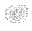
- FIG. 2 is a view taken along the line AA in FIG. 1 and shows a state in which the connector (34) and the cover (35) are removed.
- FIG. 3 is an electric circuit diagram of an embodiment of the pressure sensor according to the present invention.
- the pressure sensor 1 includes a pressure detection element 21 inside, a pressure detection unit 2 to which a fluid inflow unit 22 is connected, and surrounds the pressure detection unit 2.
- a wiring board (hereinafter referred to as “board”) 31 connected to the pressure detecting element 21 and a connector connecting portion 3 that accommodates an external output lead wire 32 are provided.
- the pressure detection unit 2 includes a pressure detection element 21, a base 23, a receiving member 24 arranged to face the base 23, and a diaphragm 25 sandwiched between the base 23 and the receiving member 24.
- An insulating liquid such as oil is sealed in the pressure receiving space 26 between the base 23 and the diaphragm 25.
- the pressure detection element 21 is fixed to the base 23 inside the pressure receiving space 26 and faces the diaphragm 25.
- a pressurizing space 27 as a pressure introducing space is formed between the receiving member 24 and the diaphragm 25, and the internal space of the fluid inflow portion 22 communicates with the pressurizing space 27.
- the base 23 is formed in a lid shape, and the pressure detection element 21 is fixed to the lower surface of the base 23.
- the receiving member 24 is formed in a dish shape that opens upward, and the fluid inflow portion 22 is brazed and fixed to the central opening.
- the diaphragm 25 has its outer peripheral edge sandwiched between the flange of the base 23 and the flange of the receiving member 24, and these three members 23 to 25 are located at the outer peripheral edge where the outer peripheral edge of the diaphragm 25 is exposed. They are welded simultaneously by laser welding or the like and integrated as the pressure detection unit 2.
- the pressure receiving space 26 after a liquid (oil) is injected from a filling hole (not shown) formed through the base 23, the filling hole is sealed by a ball 28 on the upper surface of the base 23.
- the pressure detection element 21 is, for example, a piezo element.
- This piezo element is a kind of ferroelectric substance and is also called a piezoelectric element. When a force such as vibration or pressure is applied, a voltage is generated. When it is added, it expands and contracts.
- the pressure detection element 21 includes an output terminal, an adjustment terminal, and an EPROM writing terminal. These terminals are bonding pads provided on the pressure detection element 21.
- the output terminal includes a Vcc terminal 21b for power input, a Vout terminal 21c for signal output, and a GND terminal 21d for grounding.
- the adjustment terminals include a DS terminal 21e for serial data input / output, a CLK terminal 21f for shift register clock input, and an enable terminal (E terminal) 21g for controlling the validity of the adjustment signal. It consists of.
- the EPROM writing terminal is composed of a control gate terminal 21i and a drain terminal 21h.
- Each terminal is electrically connected to eight lead pins that pass through a through hole 23 a formed in the base 23 via a bonding wire 29.
- the lead pins are GND lead pins 33A, which are three output lead pins, signal output lead pins 33B, voltage supply lead pins 33C (these three lead pins 33A to 33C are collectively referred to as output lead pins), and the same three lead pins.
- the output lead pin is for outputting a voltage signal corresponding to the pressure detected by the pressure detection element 21 to the outside, and the adjustment lead pin and the EPROM write lead pin are voltage correction at the time of manufacture as described above. It is used for business.
- one of the output lead pins (33A to 33C) and the adjustment lead pin 36 (36B) has its upper end fixed to the substrate 31.
- three wiring patterns 50 made of metal foil for connecting and fixing the output lead pins 33A to 33C are formed, and a metal foil 51 for fixing the adjustment lead pin 36B is formed. Is formed.
- the substrate 31 is formed with a notch 31a so as to expose the upper side of the EPROM drain lead pin 37A for writing the EPROM.
- the three wiring patterns 50 are formed to connect the output lead pins 33A to 33C and each of the three external output lead wires 32 connected to the substrate 31 via the connector 34.
- the metal foil 51 is provided only for fixing the adjustment lead pin 36B to the substrate 31. Even if the adjustment lead pin 36B is connected to the metal foil 51, the adjustment lead pin 36B may be connected to another lead pin. They are not connected to the external output lead wires and are electrically disconnected from these.
- the three lead wires 32 are connected to output lead pins 33A to 33C through connectors 34, respectively.
- the adjustment lead pins 36A to 36C and the EPROM writing lead pins 37A and 37B are only used for adjustment before actual use of the pressure sensor 1, and are not connected to the lead wires. Accordingly, as shown in FIG.
- each lead pin is arranged on a substantially annular shape with the pressure detection element 21 as the center, and the external output lead wire 32 is arranged in the direction of the central axis of the pressure detection element 21 (the relevant pressure If the lead wire 33A to 33C for output and the lead wire 32 for external output are eccentric with each other in the case of being pulled out in the direction of the central axis of the sensor 1, the external output lead wire 32 is simply connected by the substrate 31 for external output. When a tensile force or the like is applied to the lead wire 32, a lateral stress is applied to the output lead pins 33A to 33C to deform them, and the hermetic seals 20d to 20f to be described later surrounding the output lead pins 33A to 33C and 20h may be destroyed.
- the adjustment lead pin 36B located on the opposite side of the output lead pins 33A to 33C with respect to the pressure detection element 21 (in other words, the center of the above-described ring) is provided on the substrate 31.
- the output lead pins 33A to 33C are adjusted. There is no possibility that the hermetic seals 20d to 20f and 20h surrounding each of the lead pins 36B for use will be broken.
- an EPROM drain lead pin 37A which is one of the EPROM write lead pins, has a portion protruding from the base 23 formed shorter than the other lead pins 33A to 33C, 36A to 36C, and 37B.
- the lead pin 37A may be prepared in advance with a shorter one than the other lead pins and may be hermetically sealed.
- the lead pin 37A having the same length as the other lead pins is prepared and hermetically sealed. Thereafter, the cutting may be performed after adjusting the EPROM 21a.
- lead pins other than the lead pin 37A may be shortened similarly to the lead pin 37A.
- the through hole 23a of the base 23 is sealed so as not to leak liquid (oil) by the hermetic seals 20a to 20h after the output lead pins 33A to 33C and the adjustment lead pin 36A are inserted.
- a connector 34 is attached to the substrate 31, and a voltage signal from the pressure detecting element 21 is taken out from the external output lead wire 32 through the bonding wire 29, the output lead pin 33, the substrate 31 and the connector 34. .
- the hermetic seal 20a can be thicker in the radial direction than the other hermetic seals 20b to 20h.
- the connector connecting portion 3 includes a cover 35 that accommodates the pressure detecting portion 2 so as to be fitted to the base 23 from the outside and cover the side of the receiving member 24.
- the cover 35 also functions as a connector case that covers the substrate 31 and the connector 34.
- the cover 35 is made of a synthetic resin such as PPE, and the upper end portion that covers the connector 34 is reduced in diameter so as to surround the external output lead wire 32, and the lower end portion side that accommodates the pressure detection unit 2 is It is formed in a large diameter shape extending in a cylindrical skirt shape.
- the cover 35 is formed with an annular step portion 35a having the same diameter as the outer diameter of the base 23 on the inner peripheral side thereof on the large diameter end side, and the base 23 is formed at an annular corner portion 23b which is an outer diameter corner portion. It is mounted so as to be fitted and seated on the annular step 35a.
- the inner space of the cover 35 is divided by the base 23 inserted in the cover 35 to form a space 41.
- the output lead pin 33, the adjustment lead pin 36, the EPROM writing lead pin 37, the substrate 31, the connector 34, and the external output lead wire 32 are accommodated in the space 41.
- the space 41 is filled with an adhesive such as urethane resin having high adhesiveness and elasticity with the cover 35 and the external output lead wire 32, and then cured. This adhesive fills the space 41 so that the output lead pins 33A to 33C, the adjustment lead pins 36A to 36C, the EPROM write lead pins 37A and 37B, the substrate 31, the connector 34, and the external output lead wire 32 are buried. Therefore, the sealing function is exhibited for the components such as the substrate 31 and the connector 34.
- the pressure sensor 1 having the above configuration changes the pressure of the pressurized space 27 due to the pressure change of the fluid flowing in from the fluid inflow portion 22 and deforms the diaphragm 25. Due to the deformation of the diaphragm 25, the pressure of the liquid (oil) sealed in the pressure receiving space 26 changes, and the pressure change propagates to the pressure detection element 21.
- the pressure detected by the pressure detection element 21 is converted into a voltage, and at that time, a predetermined voltage correction corresponding to the characteristics of the pressure sensor 1 is performed by an electronic circuit provided inside the pressure detection element 21.
- the corrected voltage signal is transmitted to the external output lead wire 32 via the bonding wire 29, the output lead pins 33A to 33C, the substrate 31, and the connector 34.
- the EPROM drain lead pin 37A is shortened, and the outer shape of the hermetic seal 20a that fills the through hole through which the EPROM drain lead pin 37A is inserted is described as being simultaneously provided. Even if these configurations are individually provided, there is no problem.
- the EPROM drain lead pin 37A may have the same length as other lead pins, and the outer diameter of the hermetic seal 20a of the through hole through which the EPROM drain lead pin 37A is inserted may be increased.
- the EPROM drain lead pin 37A may be shortened so that the outer diameter of the hermetic seal 20a is equivalent to that of other hermetic seals. Even a pressure sensor having each configuration individually can exert the effect of suppressing the application of pulse noise and preventing data loss of EPROM.
- the shift register clock input terminal lead pin 36B is fixed to the substrate 31, but the adjustment lead pins 36A to 36C and the EPROM writing lead pin 37A are used.
- 37B may be fixed to the substrate 31, or three or more of the three adjustment lead pins 36A to 36C and the two EPROM writing lead pins 37A, 37B may be fixed to the substrate 31. May be. However, in the configuration in which the EPROM drain lead pin 37A is shortened, it cannot be used for fixing the substrate 31.
- the wiring board 31 is described as being provided with the notch 31a.
- the present invention is not particularly limited to this, and the wiring board 31 is extended above the lead pin 37A without providing the notch 31a. May be.
- the lead pin 37A has the same length as the other lead pins, it may be fixed to the wiring board 31 while maintaining the insulation of the lead pin 37A, like the lead pin 36B.
- the wiring board 31 may be fixed to the wiring board 31 while extending the lead pins 36A, 37B, and 36C while maintaining the insulating properties of the lead pins.
- the pressure detection unit 2 is sandwiched between the pressure detection element 21, the base 23, the receiving member 24 arranged to face the base 23, and the base 23 and the receiving member 24.
- the diaphragm 25 is provided, but the present invention is not limited to this.
- the diaphragm is fixed to the base 23 (or a member that supports the pressure detecting element 21) by an appropriate method (for example, welding) and pressure is applied.
- the detection unit may be configured and the receiving member 24 may be omitted.
- the first embodiment has a configuration for preventing bit omission at the time of EPROM writing.
- the data of “0” in the EPROM 21a. May be rewritten to “1”.
- a structure for preventing the rewriting phenomenon of data in the EPROM in this pressure sensor will be described.
- the length of the EPROM drain lead pin 37A connected to the drain terminal 21h is shortened, and the hermetic seal 20a filling the through hole through which the lead pin 37A is inserted.
- a configuration having an enlarged outer shape or a configuration having both is shown.
- the data rewrite prevention structure in the EPROM in the second embodiment has three adjustment terminals (ie, a DS terminal 21e for serial data input / output, a CLK terminal 21f for shift register clock input, and an adjustment).
- 5 lead pins 36A, 36B and 36C connected to an enable terminal (E terminal) 21g) and two EPROM write terminals (drain terminal 21h and control gate terminal 21i), respectively, for controlling the validity of the signal for use
- E terminal enable terminal
- drain terminal 21h and control gate terminal 21i control gate terminal 21i
- the configuration of shortening the length and the outer shape of the hermetic seal filling the through-hole through which the lead pin is inserted are increased, and the noise resistance of at least one lead pin is increased. It is configured to be different from other lead pins. It is intended. Since the specific structure is the same as that of the first embodiment, the description thereof is omitted.
- the lead pin having a different noise resistance effect can be obtained. Since there is one or more, noise from the lead pin can be made difficult to be injected into each terminal of the pressure detection element 21, so that the noise applied to the terminal of the pressure detection element 21 connected to the lead pin is other This is different from the noise applied to the terminal connected to the lead pin, and rewriting of data in the EPROM 21a can be prevented.
- the drain terminal 21h is used as the terminal that enhances the noise tolerance effect, thereby preventing both data bit omission due to pulse noise application and data rewriting.
- the data rewriting may be prevented by increasing the noise resistance effect of any one of the control gate terminal 21i, E terminal 21g, DS terminal 21e, CLK terminal 21f, and E terminal 21g.
- the drain terminal 21h and at least one of the control gate terminal 21i, the DS terminal 21e, the CLK terminal 21f, and the E terminal 21g may be selected as a terminal for increasing the noise tolerance effect.
Landscapes
- Physics & Mathematics (AREA)
- General Physics & Mathematics (AREA)
- Measuring Fluid Pressure (AREA)
Abstract
書き込み端子及び調整用端子へのパルスノイズの印加によるEPROMのデータ消失及び書き換わりを防止することが可能な圧力センサを提供する。 EPROMが具備するEPROMドレイン端子(21h)と接続するEPROMドレイン用リードピン(37A)の長さを、他のリードピンより短くし、また、EPROMドレイン用リードピン(37A)が挿通される貫通孔(23a)を充填するハーメチックシールの径を大きくすることによって、EPROMドレイン端子(21h)とこれに接続するEPROMドレイン用リードピン(37A)にパルスノイズが印加されることを防止し、EPROM(21a)のデータ消失及びデータの書き換わりを防ぐことが可能となる。
Description
本発明は、EPROM及びEPROMへの書き込み用端子を有する圧力検出素子を具備する圧力センサに関し、特に、EPROM書き込み用端子に印加される高電圧パルスノイズ等によってEPROMに記憶された情報が消去されたり、書き換わったりすることを防止することが可能な圧力センサに関する。
従来、EPROM(Erasable Programmable Read Only Memory)等の不揮発性メモリを具備する圧力検出素子が収容された受圧空間内に液体を封入し、圧力検出室に外部から加えられた圧力を液体を介して圧力検出素子に伝えることで、圧力検出素子から外部圧力に応じた電圧信号を出力する圧力センサが種々提案されている。
上記液封入式圧力センサの一例として、特許文献1には、流体圧力をダイアフラムで受圧し、封入液を介して伝達された圧力をセンサチップ(圧力検出素子)によって検出し、検出した圧力を電圧に変換し、ボンディングワイヤによりベースの同心円上に配置された複数の電極ピン(リードピン)と接続され、配線基板を介して外部に出力する圧力センサが記載されている。
また、圧力センサの圧力検出素子から出力された電圧は、製造時や部品のばらつきによりそのまま外部出力とすることはできず、個々の圧力センサの特性に応じた補正・調整が必須となる。当該補正・調整は近年ではデジタルトリミングの手法が採用され、例えば特許文献2に記載のように、予め補正情報をリードオンリーメモリへ記憶させ、圧力計測時に記憶した情報を読み出して電圧を補正することにより行われる。
この場合、リードピンは、出力用の他、上記電圧補正用(以下「調整用」という。)のものも配設される。出力用リードピンは、配線基板に半田付けされ、圧力検出素子からの電圧信号を配線基板を介して、例えば当該圧力センサの中心から引き出される外部出力用リード線へ伝達するが、調整用リードピンは、専ら製造の際に補正情報を記憶する場合にのみ用いられ、外部出力用リード線と接続されない。また、出力用リードピンと調整用リードピンは、圧力検出素子の構造や上記調整作業のし易さを考慮し、各グループ毎に区分して配設されるのが通常である。
しかし、公知構造の圧力センサにおいては、EPROMのデータが消失してしまう事象を生ずる場合があることが判明し、この原因を調査した結果、圧力検出素子に高電圧のパルスノイズ等が印加されることによってEPRОM内のデータ消失となっていたことを突き止めた。更に詳細に原因を調査すると、EPROMドレイン端子に繰り返し高電圧のパルスノイズが印加されることで、フローティングゲートに蓄えられた電荷が低下し、EPROMに記憶するデータにおいてビット抜けが生じる、即ち記憶データの消失が発生することがある。これによって圧力検出素子の出力信号が不正となり、結果として圧力センサが正しく動作しなくなるということが生じていることが判明した。
また、上記のようなEPROMに記憶するデータにおいて1が0に変わるビット抜けに加え、サージなどの外来ノイズが複数の書き込み端子や調整用端子に同時に注入されると、圧力検出素子内のEPROMに記憶するデータが、0から1へと書き換わってしまう現象が確認されている。
そこで、本発明は、上記課題を解決するためになされたものであって、圧力検出素子のEPROM書き込み端子に高電圧のパルスノイズが印加されてもEPROMに記憶される種々のデータの消失(ビットが「1」から「0」となる現象)及びデータの書き換わり(ビットが「0」から「1」となる現象)を防止することが可能な圧力センサを提供することを目的とする。
上記目的を達成するため、本発明の圧力センサは、べース、該ベースとの間で受圧空間を形成するダイアフラム及び該受圧空間内に設けられた圧力検出素子を有する圧力検出部を具備し、該圧力検出素子は、不揮発性メモリと、不揮発性メモリ書き込み用端子であるコントロールゲート端子及びドレイン端子と、調整用端子であるイネーブル端子、データ入出力端子及びシフトレジスタ用クロック入力端子を有する圧力センサであって、2つの不揮発性メモリ書き込み用端子及び3つの調整用端子のうち、少なくとも1つの端子を選択し、他の前記不揮発性メモリ書き込み用端子又は前記調整端子よりもノイズ耐性効果の高い端子とすることを特徴とする。
上記圧力センサにおいて、前記不揮発性メモリ書き込み用端子であるコントロールゲート端子及びドレイン端子、及び前記調整用端子であるイネーブル端子、データ入出力端子及びシフトレジスタ用クロック入力端子は、夫々リードピンに接続されることを特徴とする。
上記圧力センサにおいて、前記ノイズ耐性効果の高い端子として選択した端子に接続するリードピンを、他の端子に接続するリードピンよりも短くすることで、他の端子よりもノイズ耐性効果を高くすることを特徴とする。
上記圧力センサにおいて、前記リードピンは、前記ベースに形成された挿通孔に挿通され、該挿通孔はハーメチックシールによって封じるよう構成され、前記挿通孔のうち、前記ノイズ耐性効果の高い端子として選択した端子と接続するリードピンを挿通する挿通孔を、他の端子と接続するリードピンを挿通する挿通孔の少なくとも1つよりも径方向に大きくし、前記ノイズ耐性効果の高い端子として選択した端子と接続するリードピンの挿通孔を封じるハーメチックシールの外形を大きくするよう構成したことを特徴とする。
上記圧力センサにおいて、前記ノイズ耐性効果を高くする端子を、前記ドレイン端子とすることを特徴とする。
上記圧力センサにおいて、前記ノイズ耐性効果を高くする端子を、前記コントロールゲート端子とすることを特徴とする。
上記圧力センサにおいて、前記ノイズ耐性効果を高くする端子を、前記イネーブル端子とすることを特徴とする。
上記圧力センサにおいて、前記ノイズ耐性効果を高くする端子を、前記データ入出力端子とすることを特徴とする。
上記圧力センサにおいて、前記ノイズ耐性効果を高くする端子を、前記シフトレジスタ用クロック入力端子とすることを特徴とする。
以上のように、本発明によれば、圧力センサの圧力検出素子が具備するEPROM等の不揮発性メモリに記憶される各種データに対して、パルスノイズ等によるデータ消失及びデータ書き換わりの虞から保護することができる。
次に、本発明を実施するための形態について、図面を参照しながら詳細に説明する。
まず、EPROM書き込み時のビット抜け(記憶データの消失)を防止するための構成を実施例1に基づき説明する。
まず、EPROM書き込み時のビット抜け(記憶データの消失)を防止するための構成を実施例1に基づき説明する。
図1に示されるように、本発明の実施例1の圧力センサ1は、内部に圧力検出素子21を有すると共に、流体流入部22が接続される圧力検出部2と、圧力検出部2を囲繞すると共に、圧力検出素子21に接続される配線基板(以下「基板」という。)31や外部出力用リード線32を収容するコネクタ接続部3とを備える。
圧力検出部2は、圧力検出素子21と、ベース23と、ベース23に対向して配置された受け部材24と、ベース23と受け部材24とで挟持されたダイアフラム25とを備える。ベース23とダイアフラム25との間の受圧空間26には、オイル等の絶縁性の液体が封入される。圧力検出素子21は、受圧空間26の内部でベース23に固定され、ダイアフラム25と対向する。受け部材24とダイアフラム25との間には圧力導入空間としての加圧空間27が形成され、加圧空間27には流体流入部22の内部空間が連通する。
ベース23は蓋状に形成され、ベース23の下面には圧力検出素子21が固定される。受け部材24は上方が開口する皿状に形成され、中心部開口に流体流入部22がろう付け固定される。ダイアフラム25は、その外周縁部がベース23の鍔部と受け部材24の鍔部との間に挟み込まれ、これら3つの部材23~25は、ダイアフラム25の外周縁部が露出する外周縁部分においてレーザー溶接等によって同時に溶接され、圧力検出部2として一体化される。受圧空間26は、ベース23を貫通して形成された充填孔(不図示)から液体(オイル)が注入された後、ベース23の上面において、充填孔がボール28によって封じられる。
圧力検出素子21は、例えば、ピエゾ素子であって、このピエゾ素子は、強誘電体の一種であって圧電素子とも呼ばれ、振動や圧力等の力が加わると電圧が発生し、逆に電圧が加えられると伸縮する。
圧力検出素子21は、図3に示すように、出力用端子と調整用端子とEPROM書き込み用端子を具備する。これらの端子は圧力検出素子21に設けられたボンディングパッドである。出力用端子は、電源入力用のVcc端子21bと、信号出力用のVout端子21cと、グランドを取るためのGND端子21dとから構成される。また、調整用端子は、シリアルデータ入出力のためのDS端子21eと、シフトレジスタ用クロック入力のためのCLK端子21fと、調整用信号の有効無効を制御するためのイネーブル端子(E端子)21gとから構成される。EPROM書き込み用端子はコントロールゲート端子21iと、ドレイン端子21hとから構成される。夫々の端子は、ベース23に形成された貫通孔23aを挿通する8本のリードピンとボンディングワイヤ29を介して電気的に接続される。リードピンは、3本の出力用リードピンであるGND用リードピン33A、信号出力用リードピン33B、電圧供給用リードピン33C(これら3本のリードピン33A~33Cを総じて出力用リードピンと称呼する)、同じく3本の調整用リードピンであるシリアルデータ入出力端子用リードピン36A、シフトレジスタ用クロック入力端子用リードピン36B、イネーブル端子用リードピン36C(これら3本のリードピン36A~36Cを総じて調整用リードピンと称呼する)、及び2本のEPROM書き込み用リードピンであるEPROMドレイン用リードピン37A、EPROMコントロールゲート用リードピン37B(これら2本のリードピン37A、37Bを総じてEPROM書き込み用リードピンと称呼する)から構成される。出力用リードピンは、圧力検出素子21で検出された圧力に応じた電圧信号を外部に出力するためのものであり、調整用リードピン及びEPROM書き込み用リードピンは、上述のように、製造時の電圧補正用等に用いられるものである。
また、出力用リードピン(33A~33C)、及び調整用リードピン36のうちの1本(36B)は、各々の上端部が基板31に固定される。基板31の表面には、出力用リードピン33A~33Cを夫々接続し固定するための、金属箔からなる3つの配線パターン50が形成されると共に、調整用リードピン36Bを固定するための金属箔51が形成されている。また、基板31にはEPROM書き込み用のEPROMドレイン用リードピン37Aの上方を露出させるために切欠部31aが形成されている。
3つの配線パターン50は、各出力用リードピン33A~33Cと、コネクタ34を介して基板31に接続される3つの外部出力用リード線32の各々とを接続するために形成されている。
金属箔51は、調整用リードピン36Bを基板31に固定するためだけに設けられており、金属箔51に調整用リードピン36Bを接続しても、調整用リードピン36Bは、他のリードピンと接続されたり、外部出力用リード線と接続されたりすることはなく、これらと電気的には遮断されている。
3本のリード線32は、それぞれコネクタ34を介して出力用リードピン33A~33Cに接続される。一方、調整用リードピン36A~36C及びEPROM書き込み用リードピン37A、37Bは、当該圧力センサ1の実使用前の調整用に使われるのみなので、リード線には接続されない。従って、図1に示されるように、各リードピンが、圧力検出素子21を中心として略円環上に配置されており、かつ外部出力用リード線32が圧力検出素子21の中心軸方向(当該圧力センサ1の中心軸方向)に引き出すようにされている場合、出力用リードピン33A~33Cと外部出力用リード線32とは偏心しているから、単にこれらを基板31で接続しただけでは、外部出力用リード線32に引張力等が加えられたときに、出力用リードピン33A~33Cに横方向の応力が加わってこれが変形し、また各出力用リードピン33A~33Cを取り囲む後述のハーメチックシール20d~f及び20hが破壊されるおそれがある。
しかし、本実施例1のように、圧力検出素子21(換言すれば、上記の円環の中心)に対して各出力用リードピン33A~33Cと反対側に位置する調整用リードピン36Bを基板31に固定することにより、外部出力用リード線32に引張力等が加えられても、出力用リードピン33A~33Cに横方向の応力が加わることがなく、この結果、各出力用リードピン33A~33C、調整用リードピン36Bの夫々を取り囲むハーメチックシール20d~f及び20hが破壊されるおそれがない。
このように、出力用リードピン33A~33Cだけでなく、本来、基板31に固定する必要がない調整用リードピン36Bを基板31に固定することによって、出力用リードピン33A~33C、基板31及び調整用リードピン36Bの全体構造の強度が高まり、出力用リードピン33A~33Cの周りの構造上の脆弱性を改善することができる。
図1に示すように、EPROM書き込み用リードピンの1つであるEPROMドレイン用リードピン37Aは、ベース23から突出する部分を他のリードピン33A~33C、36A~36C及び37Bよりも短く形成している。この場合、リードピン37Aは、予め他のリードピンよりも短いものを準備して、これにハーメチックシールをしても良いが、他のリードピンと同じ長さのものを準備し、これにハーメチックシールをした後、EPROM21aに対する調整作業を経てから切断する様にしても良い。これによってEPROMドレイン用リードピン37Aがベース23から突出した部分に対して外部からの放射パルスノイズの影響を低減することができる。なお、リードピン37A以外のリードピンをリードピン37Aと同様に短くしても良い。
ベース23の貫通孔23aは、出力用リードピン33A~33C及び調整用リードピン36Aを挿通させた後、ハーメチックシール20a~hによって液体(オイル)漏れがないように封じられる。基板31には、コネクタ34が取り付けられ、圧力検出素子21からの電圧信号は、ボンディングワイヤ29、出力用リードピン33、基板31及びコネクタ34を介して外部出力用リード線32から外部へと取り出される。
図2に示すように、このハーメチックシール20a~hにおいて、EPROM書き込み用リードピンであるEPROMドレイン用リードピン37Aを挿通する貫通孔23aは、他の貫通孔23aよりも径方向に大きく形成される。従ってハーメチックシール20aを他のハーメチックシール20b~20hよりも径方向に厚みを持たせることができる。EPROMドレイン37Aのハーメチックシール20aの外形を大きくすることによって、ベース23とリードピン37Aとの絶縁距離が長くなるため、EPROMドレイン37Aに印加されるパルスノイズを低減することが可能となる。
コネクタ接続部3は、ベース23に外側から嵌合して受け部材24の側方を覆うように圧力検出部2を収容するカバー35を備える。カバー35は、基板31及びコネクタ34を覆うコネクタケースとしても機能する。このカバー35は、PPE等の合成樹脂製で形成され、コネクタ34を覆う上端部は、外部出力用リード線32を囲繞するように縮径され、圧力検出部2を収容する下端部側は、筒状スカート状に延びる大径状に形成される。
カバー35は、大径端部側において、その内周側にベース23の外径と略同径の環状段部35aが形成され、ベース23は、その外径角部である環状角部23bにおいて環状段部35aに嵌合座着するように載置される。
カバー35の内部空間は、カバー35に装入されたベース23で区切られ、空間41が形成される。出力用リードピン33と、調整用リードピン36と、EPROM書き込み用リードピン37と、基板31と、コネクタ34と、外部出力用リード線32とは、空間41に収容される。空間41には、カバー35や外部出力用リード線32との接着性及び弾性の大きいウレタン樹脂等の接着剤が充填され、その後、硬化される。この接着剤は、出力用リードピン33A~33C、調整用リードピン36A~36C、EPROM書き込み用リードピン37A及び37B、基板31、コネクタ34及び外部出力用リード線32が埋設状態になるように空間41に充填されるので、基板31やコネクタ34等の部品に対して封止機能を奏する。
また、この接着剤の硬化にはある程度の時間を要するが、接着剤の硬化に至るまでの間に外部出力用リード線に引張力等が加えられても、前述のように、リードピンの変形やハーメチックシール20a~hの破壊が防止される。もちろん、接着剤の硬化後も上記変形や破壊の防止効果は達成される。また、受け部材24とカバー35とにより形成される空間42も、樹脂等で封止される。
上記構成を有する圧力センサ1は、流体流入部22から流入した流体の圧力変化によって加圧空間27の圧力が変化し、ダイアフラム25を変形させる。ダイアフラム25の変形により受圧空間26の内部に封入されている液体(オイル)の圧力が変化し、その圧力変化が圧力検出素子21へ伝播する。圧力検出素子21により検出された圧力は、電圧に変換され、その際、圧力検出素子21の内部に設けられた電子回路により、圧力センサ1の特性に応じた所定の電圧補正がなされる。補正後の電圧信号は、ボンディングワイヤ29、出力用リードピン33A~33C、基板31及びコネクタ34を介して外部出力用リード線32へ伝送される。
なお、上記実施例1において、EPROMドレイン用リードピン37Aを短くする構成と、EPROMドレイン用リードピン37Aを挿通する貫通孔を充填するハーメチックシール20aの外形を大きくする構成とを同時に備えるものとして説明したが、これらの構成を個別に備えたとしても何ら問題ない。例えばEPROMドレイン用リードピン37Aを他のリードピンと同等の長さとし、EPROMドレイン用リードピン37Aを挿通する貫通孔のハーメチックシール20aの外径を大きくする構成としてもよい。逆にEPROMドレイン用リードピン37Aを短くし、ハーメチックシール20aの外径を他のハーメチックシールと同等とする構成としてもよい。各々の構成を夫々単独に備えた圧力センサであっても、パルスノイズの印加を抑制し、EPROMのデータ消失を防止する効果を発揮することが可能である。
また、上記実施例1においては、3本の調整用リードピン36A~36Cのうちのシフトレジスタ用クロック入力端子用リードピン36Bを基板31に固定したが、調整用リードピン36A~36C及びEPROM書き込み用リードピン37A、37Bのいずれか一つのみを基板31に固定してもよく、また、3本の調整用リードピン36A~36C及び2本のEPROM書き込み用リードピン37A、37Bのうち3本以上を基板31に固定してもよい。但し、EPROMドレイン用リードピン37Aを短くする構成において、これを基板31の固定に用いることはできない。
さらに配線基板31には切欠部31aが設けられるものとして説明したが、本発明は特にこれのみに限定されることはなく、切欠部31aを設けずに配線基板31をリードピン37Aの上方に延長してもよい。この場合、リードピン37Aを他のリードピンと同じ長さにする場合はリードピン36Bと同様に、リードピン37Aの絶縁性を保ちつつ配線基板31に固定しても良い。
さらにまた、配線基板31をリードピン36A、37B、36Cの上方に延長する様にして、それらリードピンの絶縁性を保ちつつ配線基板31に固定しても良いことは当然である。
さらにまた、前述の説明においては、圧力検出部2は、圧力検出素子21と、ベース23と、ベース23に対向して配置された受け部材24と、ベース23と受け部材24とで挟持されたダイアフラム25とを備えるものとしたが、本発明はこれのみに限定されることはなく、ベース23(あるいは圧力検出素子21を支持する部材)にダイアフラムを適宜の手法(例えば溶接)により固着し圧力検出部を構成し、受け部材24を省略するようにしても良い。
さらにまた、配線基板31をリードピン36A、37B、36Cの上方に延長する様にして、それらリードピンの絶縁性を保ちつつ配線基板31に固定しても良いことは当然である。
さらにまた、前述の説明においては、圧力検出部2は、圧力検出素子21と、ベース23と、ベース23に対向して配置された受け部材24と、ベース23と受け部材24とで挟持されたダイアフラム25とを備えるものとしたが、本発明はこれのみに限定されることはなく、ベース23(あるいは圧力検出素子21を支持する部材)にダイアフラムを適宜の手法(例えば溶接)により固着し圧力検出部を構成し、受け部材24を省略するようにしても良い。
上記実施例1は、EPROM書き込み時のビット抜けを防止するための構成であるが、EPROM書き込み用端子及び調整用端子に同時に同種のノイズが印加されると、EPROM21a内の「0」であるデータが「1」に書き換わる現象が発生することがある。以下、この圧力センサにおけるEPROM内データの書き換わり現象の防止構造について説明する。
上記実施例1では、EPROMのデータ消失を防止する構成として、ドレイン端子21hに接続するEPROMドレイン用リードピン37Aの長さを短くする構成や、リードピン37Aを挿通する貫通孔を充填するハーメチックシール20aの外形を大きくする構成、またはその両方を備える構成を示した。
それに対し、本実施例2におけるEPROM内データの書き換わり防止構造は、3つの調整用端子(すなわちシリアルデータ入出力のためのDS端子21e、シフトレジスタ用クロック入力のためのCLK端子21f、及び調整用信号の有効無効を制御するためのイネーブル端子(E端子)21g)並びに2つのEPROM書き込み用端子(ドレイン端子21h及びコントロールゲート端子21i)のそれぞれと接続する5本のリードピン36A、36B及び36C、並びに37A及び37Bの少なくとも何れか1つに対して、長さを短くする構成や、当該リードピンを挿通する貫通孔を充填するハーメチックシールの外形を大きくし、少なくとも1本以上のリードピンのノイズ耐性を高めることで、他のリードピンと相違するよう構成するものである。具体的な構造については先の実施例1と同様であるため、その説明を省略する。
このような構成とすることで、圧力検出素子21が有するEPROM書き込み用端子及び調整用端子に同時に同種のノイズが印加されたとしても、ノイズ耐性効果が異なる(あるいはノイズ耐性効果が高い)リードピンが1つ以上存在することから、当該リードピンからのノイズは圧力検出素子21の各端子に注入されにくくすることができるので、当該リードピンと接続する圧力検出素子21の端子に印加されるノイズは、他のリードピンと接続する端子に印加されるノイズとは別種のものとなり、EPROM21a内のデータの書き換わりを防ぐことが可能となる。
尚、少なくとも1つのリードピンの寸法を、他のリードピンの寸法と変えることで同時に同種のノイズが各リードピンに印加されることを防止することが可能であるため、1つ以上のリードピンを他のリードピンよりも長くすることでも、同様の効果を得ることができる。しかしながらリードピンを長くすることは多様なノイズのアンテナとなってしまい、その影響を受けやすくしてしまうことから、リードピンの長さを変える場合は、他のリードピンよりも短くするよう構成することが望ましい。また、短くするリードピンは多い方がEPROM21a内のデータの書き換わりを効果的に防止することが可能となる。
上記各実施例からも分かる通り、ノイズ耐性効果を高くする端子をドレイン端子21hとすることで、パルスノイズ印加によるデータのビット抜けと、データの書き換わりの双方を防止することが可能である。当然、コントロールゲート端子21i、E端子21g、DS端子21e、CLK端子21f、E端子21gの何れかのノイズ耐性効果を高くすることで、データの書き換わりを防止する構成としてもよい。さらにまた、ノイズ耐性効果を高くする端子として、ドレイン端子21hと、コントロールゲート端子21i、DS端子21e、CLK端子21f、及びE端子21gの少なくとも1つとを選択しても良い。
1 圧力センサ
2 圧力検出部
3 コネクタ接続部
20a~20h ハーメチックシール
21 圧力検出素子
21a EPROM(不揮発性メモリ)
21b、21c、21d 出力用端子
21e、21f、21g 調整用端子
21h、21i EPROM書き込み用端子
22 流体流入部
23 ベース
23a 貫通孔
23b 環状角部
24 受け部材
25 ダイアフラム
26 受圧空間
27 加圧空間
28 ボール
29 ワイヤ
31 配線基板
31a 切欠部
32 外部出力用リード線
33A GND用リードピン
33B 信号出力用リードピン
33C 電圧供給用リードピン
34 コネクタ
35 カバー
35a 環状段部
36A シリアルデータ入出力端子用リードピン
36B シフトレジスタ用クロック入力端子用リードピン
36C イネーブル端子用リードピン
37A EPROMドレイン用リードピン
37B EPROMコントロールゲート用リードピン
38A GND用接続端子
38B 電圧供給用接続端子
38C 信号出力用接続端子
41 空間
42 空間
50 配線パターン
51 金属箔
2 圧力検出部
3 コネクタ接続部
20a~20h ハーメチックシール
21 圧力検出素子
21a EPROM(不揮発性メモリ)
21b、21c、21d 出力用端子
21e、21f、21g 調整用端子
21h、21i EPROM書き込み用端子
22 流体流入部
23 ベース
23a 貫通孔
23b 環状角部
24 受け部材
25 ダイアフラム
26 受圧空間
27 加圧空間
28 ボール
29 ワイヤ
31 配線基板
31a 切欠部
32 外部出力用リード線
33A GND用リードピン
33B 信号出力用リードピン
33C 電圧供給用リードピン
34 コネクタ
35 カバー
35a 環状段部
36A シリアルデータ入出力端子用リードピン
36B シフトレジスタ用クロック入力端子用リードピン
36C イネーブル端子用リードピン
37A EPROMドレイン用リードピン
37B EPROMコントロールゲート用リードピン
38A GND用接続端子
38B 電圧供給用接続端子
38C 信号出力用接続端子
41 空間
42 空間
50 配線パターン
51 金属箔
Claims (9)
- ベース、該ベースとの間で受圧空間を形成するダイアフラム及び該受圧空間内に設けられた圧力検出素子を有する圧力検出部を具備し、
該圧力検出素子は、不揮発性メモリと、不揮発性メモリ書き込み用端子であるコントロールゲート端子及びドレイン端子と、調整用端子であるイネーブル端子、データ入出力端子及びシフトレジスタ用クロック入力端子を有する圧力センサであって、
2つの不揮発性メモリ書き込み用端子及び3つの調整用端子のうち、少なくとも1つの端子を選択し、他の前記不揮発性メモリ書き込み用端子又は前記調整端子よりもノイズ耐性効果の高い端子とすることを特徴とする圧力センサ。 - 前記不揮発性メモリ書き込み用端子であるコントロールゲート端子及びドレイン端子、及び前記調整用端子であるイネーブル端子、データ入出力端子及びシフトレジスタ用クロック入力端子は、夫々リードピンに接続されることを特徴とする請求項1記載の圧力センサ。
- 前記ノイズ耐性効果の高い端子として選択した端子に接続するリードピンを、他の端子に接続するリードピンよりも短くすることで、他の端子よりもノイズ耐性効果を高くすることを特徴とする請求項2記載の圧力センサ。
- 前記リードピンは、前記ベースに形成された挿通孔に挿通され、該挿通孔はハーメチックシールによって封じるよう構成され、
前記挿通孔のうち、前記ノイズ耐性効果の高い端子として選択した端子と接続するリードピンを挿通する挿通孔を、他の端子と接続するリードピンを挿通する挿通孔の少なくとも1つよりも径方向に大きくし、前記ノイズ耐性効果の高い端子として選択した端子と接続するリードピンの挿通孔を封じるハーメチックシールの外形を大きくするよう構成したことを特徴とする請求項2又は3に記載の圧力センサ。 - 前記ノイズ耐性効果を高くする端子を、前記ドレイン端子とすることを特徴とする請求項1乃至4の何れか一項記載の圧力センサ。
- 前記ノイズ耐性効果を高くする端子を、前記コントロールゲート端子とすることを特徴とする請求項1乃至4の何れか一項記載の圧力センサ。
- 前記ノイズ耐性効果を高くする端子を、前記イネーブル端子とすることを特徴とする請求項1乃至4の何れか一項記載の圧力センサ。
- 前記ノイズ耐性効果を高くする端子を、前記データ入出力端子とすることを特徴とする請求項1乃至4の何れか一項記載の圧力センサ。
- 前記ノイズ耐性効果を高くする端子を、前記シフトレジスタ用クロック入力端子とすることを特徴とする請求項1乃至4の何れか一項記載の圧力センサ。
Applications Claiming Priority (2)
| Application Number | Priority Date | Filing Date | Title |
|---|---|---|---|
| JP2014-079342 | 2014-04-08 | ||
| JP2014079342 | 2014-04-08 |
Publications (1)
| Publication Number | Publication Date |
|---|---|
| WO2015156291A1 true WO2015156291A1 (ja) | 2015-10-15 |
Family
ID=54287865
Family Applications (1)
| Application Number | Title | Priority Date | Filing Date |
|---|---|---|---|
| PCT/JP2015/060881 Ceased WO2015156291A1 (ja) | 2014-04-08 | 2015-04-07 | 圧力センサ |
Country Status (1)
| Country | Link |
|---|---|
| WO (1) | WO2015156291A1 (ja) |
Cited By (1)
| Publication number | Priority date | Publication date | Assignee | Title |
|---|---|---|---|---|
| WO2019240945A1 (en) | 2018-06-12 | 2019-12-19 | Dwyer Instruments, Inc. | Electrostatic discharge resistantpressure sensor |
Citations (4)
| Publication number | Priority date | Publication date | Assignee | Title |
|---|---|---|---|---|
| JPH04118974A (ja) * | 1990-09-10 | 1992-04-20 | Fujitsu Ltd | 半導体不揮発性記憶装置及びその製造方法 |
| JP2003270069A (ja) * | 2002-03-14 | 2003-09-25 | Denso Corp | センサ装置 |
| JP2004165275A (ja) * | 2002-11-11 | 2004-06-10 | Renesas Technology Corp | デジタルトリミングシステム |
| JP2005308503A (ja) * | 2004-04-20 | 2005-11-04 | Toyoda Mach Works Ltd | 半導体センサ |
-
2015
- 2015-04-07 WO PCT/JP2015/060881 patent/WO2015156291A1/ja not_active Ceased
Patent Citations (4)
| Publication number | Priority date | Publication date | Assignee | Title |
|---|---|---|---|---|
| JPH04118974A (ja) * | 1990-09-10 | 1992-04-20 | Fujitsu Ltd | 半導体不揮発性記憶装置及びその製造方法 |
| JP2003270069A (ja) * | 2002-03-14 | 2003-09-25 | Denso Corp | センサ装置 |
| JP2004165275A (ja) * | 2002-11-11 | 2004-06-10 | Renesas Technology Corp | デジタルトリミングシステム |
| JP2005308503A (ja) * | 2004-04-20 | 2005-11-04 | Toyoda Mach Works Ltd | 半導体センサ |
Cited By (5)
| Publication number | Priority date | Publication date | Assignee | Title |
|---|---|---|---|---|
| WO2019240945A1 (en) | 2018-06-12 | 2019-12-19 | Dwyer Instruments, Inc. | Electrostatic discharge resistantpressure sensor |
| KR20210033944A (ko) * | 2018-06-12 | 2021-03-29 | 드와이어 인스투르먼쓰 인코포레이티드 | 정전기 방전 저항 압력 센서 |
| EP3807208A4 (en) * | 2018-06-12 | 2022-03-09 | Dwyer Instruments, Inc. | STATIC RESISTANT PRESSURE SENSOR |
| US11435249B2 (en) | 2018-06-12 | 2022-09-06 | Dwyer Instruments, Inc. | Electrostatic discharge resistant pressure sensor |
| KR102533097B1 (ko) * | 2018-06-12 | 2023-05-15 | 드와이어 인스투르먼쓰 인코포레이티드 | 정전기 방전 저항 압력 센서 |
Similar Documents
| Publication | Publication Date | Title |
|---|---|---|
| JP5840172B2 (ja) | 圧力センサーおよび圧力センサーの製造方法 | |
| US10352808B2 (en) | Pressure detection unit | |
| EP2857817A1 (en) | Pressure detection device | |
| JP5833835B2 (ja) | 圧力センサ | |
| US9470598B2 (en) | Pressure detection device and method for producing same | |
| US20150177088A1 (en) | Pressure sensor | |
| JP5278143B2 (ja) | 圧力センサ | |
| CN103487198B (zh) | 压力传感器以及压力传感器的制造方法 | |
| JP2017134014A (ja) | 圧力センサ | |
| JP6394707B2 (ja) | 電子部品、特に再調整可能な感度を備えたマイクロフォン、および調整方法 | |
| WO2015156291A1 (ja) | 圧力センサ | |
| JP5966071B2 (ja) | 圧力センサ | |
| US9891128B2 (en) | Pressure sensor having a digital circuit unit connected to adjustment terminals and earth terminals | |
| WO2009087767A1 (ja) | 圧力センサ及びその製造方法 | |
| CN110418950A (zh) | 压力传感器 | |
| JP4737032B2 (ja) | コネクタ一体型センサ | |
| JP5656318B2 (ja) | 圧力センサーおよび圧力センサーの製造方法 | |
| JP2014102115A (ja) | 圧力検知ユニット及びその製造方法 | |
| JP2017092192A (ja) | 電子機器の製造方法および電子機器 | |
| JP6810680B2 (ja) | 圧力センサ | |
| JP6456314B2 (ja) | 冷媒回路構成部品 | |
| JP5720450B2 (ja) | 圧力センサおよび圧力センサの取り付け構造 | |
| CN112875636A (zh) | 封装环境传感器 | |
| WO2018055953A1 (ja) | 圧力センサ | |
| JP2017092354A (ja) | 電子機器 |
Legal Events
| Date | Code | Title | Description |
|---|---|---|---|
| 121 | Ep: the epo has been informed by wipo that ep was designated in this application |
Ref document number: 15776252 Country of ref document: EP Kind code of ref document: A1 |
|
| WA | Withdrawal of international application | ||
| NENP | Non-entry into the national phase |
Ref country code: DE |