WO2015156104A1 - プローブカバー - Google Patents
プローブカバー Download PDFInfo
- Publication number
- WO2015156104A1 WO2015156104A1 PCT/JP2015/058574 JP2015058574W WO2015156104A1 WO 2015156104 A1 WO2015156104 A1 WO 2015156104A1 JP 2015058574 W JP2015058574 W JP 2015058574W WO 2015156104 A1 WO2015156104 A1 WO 2015156104A1
- Authority
- WO
- WIPO (PCT)
- Prior art keywords
- base
- probe cover
- socket
- locking
- positioning pin
- Prior art date
- Legal status (The legal status is an assumption and is not a legal conclusion. Google has not performed a legal analysis and makes no representation as to the accuracy of the status listed.)
- Ceased
Links
Images









Classifications
-
- G—PHYSICS
- G01—MEASURING; TESTING
- G01R—MEASURING ELECTRIC VARIABLES; MEASURING MAGNETIC VARIABLES
- G01R1/00—Details of instruments or arrangements of the types included in groups G01R5/00 - G01R13/00 and G01R31/00
- G01R1/02—General constructional details
- G01R1/06—Measuring leads; Measuring probes
- G01R1/067—Measuring probes
- G01R1/073—Multiple probes
- G01R1/07307—Multiple probes with individual probe elements, e.g. needles, cantilever beams or bump contacts, fixed in relation to each other, e.g. bed of nails fixture or probe card
-
- G—PHYSICS
- G01—MEASURING; TESTING
- G01R—MEASURING ELECTRIC VARIABLES; MEASURING MAGNETIC VARIABLES
- G01R31/00—Arrangements for testing electric properties; Arrangements for locating electric faults; Arrangements for electrical testing characterised by what is being tested not provided for elsewhere
- G01R31/28—Testing of electronic circuits, e.g. by signal tracer
- G01R31/2851—Testing of integrated circuits [IC]
- G01R31/2886—Features relating to contacting the IC under test, e.g. probe heads; chucks
-
- G—PHYSICS
- G01—MEASURING; TESTING
- G01R—MEASURING ELECTRIC VARIABLES; MEASURING MAGNETIC VARIABLES
- G01R1/00—Details of instruments or arrangements of the types included in groups G01R5/00 - G01R13/00 and G01R31/00
- G01R1/02—General constructional details
- G01R1/04—Housings; Supporting members; Arrangements of terminals
-
- H—ELECTRICITY
- H01—ELECTRIC ELEMENTS
- H01R—ELECTRICALLY-CONDUCTIVE CONNECTIONS; STRUCTURAL ASSOCIATIONS OF A PLURALITY OF MUTUALLY-INSULATED ELECTRICAL CONNECTING ELEMENTS; COUPLING DEVICES; CURRENT COLLECTORS
- H01R33/00—Coupling devices specially adapted for supporting apparatus and having one part acting as a holder providing support and electrical connection via a counterpart which is structurally associated with the apparatus, e.g. lamp holders; Separate parts thereof
- H01R33/74—Devices having four or more poles, e.g. holders for compact fluorescent lamps
- H01R33/76—Holders with sockets, clips, or analogous contacts adapted for axially-sliding engagement with parallely-arranged pins, blades, or analogous contacts on counterpart, e.g. electronic tube socket
- H01R33/7664—Holders with sockets, clips, or analogous contacts adapted for axially-sliding engagement with parallely-arranged pins, blades, or analogous contacts on counterpart, e.g. electronic tube socket having additional guiding, adapting, shielding, anti-vibration or mounting means
-
- H—ELECTRICITY
- H01—ELECTRIC ELEMENTS
- H01R—ELECTRICALLY-CONDUCTIVE CONNECTIONS; STRUCTURAL ASSOCIATIONS OF A PLURALITY OF MUTUALLY-INSULATED ELECTRICAL CONNECTING ELEMENTS; COUPLING DEVICES; CURRENT COLLECTORS
- H01R33/00—Coupling devices specially adapted for supporting apparatus and having one part acting as a holder providing support and electrical connection via a counterpart which is structurally associated with the apparatus, e.g. lamp holders; Separate parts thereof
- H01R33/74—Devices having four or more poles, e.g. holders for compact fluorescent lamps
- H01R33/76—Holders with sockets, clips, or analogous contacts adapted for axially-sliding engagement with parallely-arranged pins, blades, or analogous contacts on counterpart, e.g. electronic tube socket
- H01R33/7671—Holders with sockets, clips, or analogous contacts adapted for axially-sliding engagement with parallely-arranged pins, blades, or analogous contacts on counterpart, e.g. electronic tube socket having multiple positions or sockets, e.g. stacked sockets while mounting
Definitions
- the present invention relates to a probe cover that is attached to a socket that supports a plurality of contact probes.
- the contact probe is used, for example, to electrically connect an inspection object such as a semiconductor integrated circuit and an inspection substrate on the measuring instrument side.
- a socket supporting a plurality of contact probes is fixed to an inspection substrate, and the socket is pressed against an inspection object.
- one end of each contact probe is in contact with the electrode of the inspection substrate, and the other end is in contact with the electrode (for example, solder bump) of the inspection object.
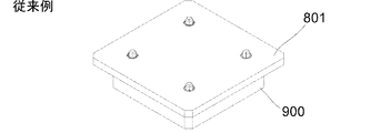
- the probe cover is fixed to the socket by screws. For example, there are 4 to 6 screwing points. 15 and 16 show a state in which the conventional probe cover 801 is screwed to the socket 900 at four locations.
- the probe cover and socket holes must be coaxial with each other.
- the present invention has been made in recognition of such a situation, and an object thereof is to provide a probe cover that can be attached to a plurality of sockets having different shapes.
- One embodiment of the present invention is a probe cover.
- This probe cover A probe cover attached to a socket supporting a plurality of contact probes, Base and Two positioning pins provided on the base; And at least one support member provided on the base, The two positioning pins and the support member can position the base with a predetermined distance from the socket. The distance between the two positioning pins can be changed.
- the mutual separation distance can be selected from continuous values.
- the base may have a guide portion that supports the two positioning pins so as to be slidable.
- both the guide portions are provided on the same straight line.
- locking means for locking one of the two positioning pins at an arbitrary slide position It is preferable to have locking means for locking one of the two positioning pins at an arbitrary slide position.
- the base has a plurality of mounting holes and the support member can be mounted in any of the mounting holes.
- the two support members are provided, and the two support members can be arranged separately on both sides across a straight line passing through the two positioning pins.
- the base has a disc shape.
- the base is transparent.
- FIG. 3 is an exploded upper perspective view of the probe cover 1.
- the disassembled lower perspective view of the probe cover 1. The top view of the probe cover 1.
- the B section enlarged view of FIG. 5 non-locking state).
- CC sectional drawing of FIG. FIG. 3 is a front sectional view of the probe cover 1.
- the D section enlarged view of FIG. The right view of the probe cover 1.
- FIG. FIG. The top perspective view of the state which screwed the conventional probe cover 801 to the socket 900.
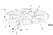
- FIG. 1 is a top perspective view of a probe cover 1 according to an embodiment of the present invention.
- FIG. 2 is a lower perspective view of the same.
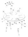
- FIG. 3 is an exploded upper perspective view of the probe cover 1.
- FIG. 4 is an exploded lower perspective view of the probe cover 1.
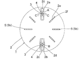
- FIG. 5 is a plan view of the probe cover 1. In FIG. 5, the stand pin 5 is highlighted by hatching.
- FIG. 6 is an enlarged view of part A in FIG.
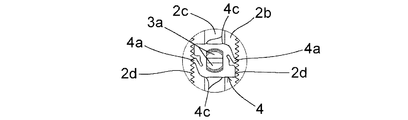
- FIG. 7 is an enlarged view (locked state) of B part in FIG.
- FIG. 8 is an enlarged view of a portion B in FIG. 5 (unlocked state).
- 9 is a cross-sectional view taken along the line CC of FIG.
- FIG. 10 is a front sectional view of the probe cover 1.
- FIG. 11 is an enlarged view of a portion D in FIG.
- FIG. 12 is a right side view of the probe cover 1.
- FIG. 13 is an upper perspective view of the probe cover 1 attached to the socket 100.
- the probe cover 1 is attached to a socket 100 that supports a plurality of contact probes, and protects the tip of each contact probe protruding from the socket 100. In FIG. 13 and FIG. 14, illustration of each contact probe supported by the socket 100 is omitted.
- the probe cover 1 includes a base 2, two positioning pins 3 having the same shape, two positioning pin holders 4 having the same shape, and two stand pins 5 having the same shape as support members.
- the shape and color of the base 2 are not particularly limited, it is preferably a disc-shaped transparent resin molded body, and is formed as such in the present embodiment.
- the positioning pin 3, the positioning pin holder 4, and the stand pin 5 are, for example, resin molded bodies.
- the base 2 has a slide guide groove 2a and a slide locking groove 2b.
- Slide guide holes 2c as guide portions are provided at the bottoms of the slide guide groove 2a and the slide locking groove 2b, respectively.
- the width of the slide guide hole 2c in the short direction (the width in the direction orthogonal to the slide direction) is smaller than the width of the slide guide groove 2a and the slide locking groove 2b in the same direction.
- the width of the slide locking groove 2b in the short direction is larger than the width of the slide guide groove 2a in the same direction so that a positioning pin holder 4 described later can be rotated.
- the slide guide groove 2 a and the slide locking groove 2 b and both slide guide holes 2 c are provided on the same straight line passing through the center of the base 2.
- locking rack portions 2d are provided along the sliding direction.
- the base 2 has a plurality of recesses 2e. Each recess 2 e extends radially from the inside to the outside of the base 2. A plurality of stand pin locking holes 2f as a plurality of mounting holes are provided on the bottom surface of each recess 2e. In the illustrated example, three recesses 2e are provided at equal angular intervals on both sides across a straight line passing through the slide guide groove 2a and the slide locking groove 2b, and five stand pin locking holes 2f are provided on the bottom surface of each recess 2e. It is provided one by one.
- the positioning pin 3 has a pair of claw portions 3a, a base portion 3b, and a pin body portion 3c.
- the pair of claw portions 3a is erected upward from the base portion 3b.
- the pin main body 3c is, for example, a columnar shape, and is erected downward from the base 3b.
- the outer diameter of the pin main body 3c is smaller than the outer diameter of the base 3b.
- the lower end surface of the base portion 3b is a mounting surface for the socket 100 (FIGS. 13 and 14).
- the pin body 3c has a socket locking projection 3d on the outer peripheral surface in the vicinity of the base 3b.
- the positioning pin holder 4 is accommodated in the slide guide groove 2a and the slide locking groove 2b, respectively.
- the upper surface of the positioning pin holder 4 is preferably substantially flush with the upper surface of the base 2.
- the positioning pin holder 4 has a pair of tongue pieces 4a (claw portions), positioning pin locking holes 4b, and a predetermined number of protrusions 4c.
- the pair of tongue pieces 4a are locked to the locking rack portion 2d of the slide locking groove 2b at a predetermined rotational position (FIG. 7).
- the locking rack portion 2d and the tongue piece portion 4a function as locking means for locking the positioning pin 3 at an arbitrary slide position.
- the positioning pin locking hole 4 b is provided in the center of the positioning pin holder 4. As shown in FIG.
- a pair of locking projections 4 d are provided on the inner surface of the positioning pin locking hole 4 b to lock the pair of claw portions 3 a of the positioning pin 3.
- two ridges 4c are provided on both side surfaces of the positioning pin holder 4 where the tongue pieces 4a are not provided so as to extend in the vertical direction.
- the protrusion 4c has a function to prevent the positioning pin holder 4 from rattling in the slide guide groove 2a (FIG. 6).
- the stand pin 5 has a stand portion 5a and a locking pin portion 5b.
- the locking pin portion 5b has, for example, a cylindrical shape and is erected at the center of the upper surface of the stand portion 5a.
- a locking recess 5c is provided on the outer peripheral surface near the tip of the locking pin 5b. As shown in FIG. 11, the locking recess 5 c is fitted to the throttle portion 2 g of the stand pin locking hole 2 f and functions as a retaining pin for the stand pin 5.
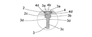
- the pair of claw portions 3a of the positioning pin 3 is positioned in the slide guide groove 2a from below via the slide guide hole 2c formed on the bottom surface of the slide guide groove 2a. Then, the positioning pin holder 4 is inserted into the slide guide groove 2a from above, and the pair of claw portions 3a of the positioning pin 3 is hooked on the pair of locking convex portions 4d in the positioning pin locking hole 4b. In this state, as shown in FIG. 9, the upper end surface of the base portion 3 b of the positioning pin 3 comes into contact with the lower end surface of the base 2 (surface around the slide guide hole 2 c).
- the positioning pin 3 sandwiches the periphery of the locking projection 4d of the positioning pin holder 4 and the slide guide hole 2c between the pair of claw portions 3a and the upper end surface of the base portion 3b, and together with the positioning pin holder 4, the slide guide groove 2a and It becomes possible to slide with a certain sliding resistance along the slide guide hole 2c (supported so as to be slidable with respect to the base 2).
- the other positioning pin 3 and positioning pin holder 4 are also attached to the base 2 in the same procedure.
- the rotation position of the positioning pin holder 4 is as shown in FIG. 8 (the tongue piece portion 4a is not engaged with the locking rack portion 2d).
- the other positioning pin 3 can slide with a certain sliding resistance along the slide guide hole 2c in the slide locking groove 2b together with the positioning pin holder 4 (being slidable with respect to the base 2). Supported).
- the positioning pin 3 and the positioning pin holder 4 may be attached to either the slide guide groove 2a side or the slide locking groove 2b side first.
- the positioning pin 3 is slid in accordance with the position of the through hole of the socket 100 to which the probe cover 1 is attached, and the positioning pin on the slide locking groove 2b side 3 and the positioning pin holder 4 are rotated by 90 ° from the non-locking state shown in FIG. 8 to the locking state shown in FIG. Accordingly, the positioning pin 3 and the positioning pin holder 4 on the slide locking groove 2b side are locked at the current slide position.
- the slide position slightly shifts when the positioning pin 3 and the positioning pin holder 4 on the slide locking groove 2b side are brought into the locked state shown in FIG. 7, the positioning on the slide guide groove 2a side that can always slide is possible. This can be dealt with by adjusting the slide positions of the pin 3 and the positioning pin holder 4.
- the locking pin portion 5b of the stand pin 5 is inserted into a desired stand pin locking hole 2f of the base 2, and the locking recess portion 5c of the locking pin portion 5b and the stand pin locking hole as shown in FIG.
- the stand pin 5 is locked in the stand pin locking hole 2f.
- the tip of the locking pin portion 5 b is located in the recess 2 e of the base 2 and does not protrude from the upper surface of the base 2.
- the attachment positions of the two stand pins 5 (which stand pin engagement holes 2f are attached) are appropriately determined according to the shape of the socket 100 to which the probe cover 1 is attached. Note that the stand pin 5 may be attached before the positioning pin 3 and the positioning pin holder 4.
- the probe cover 1 is attached to the socket 100 as shown in FIGS. To do. Specifically, the pin main body portion 3 c of the positioning pin 3 is inserted into the through hole 101 of the socket 100, and the socket locking convex portion 3 d of the pin main body portion 3 c is fitted into the through hole 101. Then, the socket locking convex portion 3d presses the inner surface of the through hole 101, generates a certain resistance against the disconnection, the pin main body portion 3c is locked to the through hole 101, and the probe cover for the socket 100. The rattling of 1 is prevented.
- the probe cover 1 is positioned and mounted on the socket 100 by the two positioning pins 3, the positioning pin holder 4 and the two stand pins 5 with the lower surface of the base 2 spaced apart from the upper surface of the socket 100 by a certain distance.
- the pin body portion 3 c of the positioning pin 3 comes out of the through hole 101 of the socket 100, and the probe cover 1 is separated from the socket 100.
- the positioning pin 3 on the slide locking groove 2b side is rotated by 90 °, the positioning pin holder 4 and the locking rack portion 2d are disengaged (FIG. 7 ⁇ FIG. 8).
- the positioning pin 3 is pulled downward while pressing and contracting the pair of claw portions 3a of the positioning pin 3, the positioning pin 3 is separated from the positioning pin holder 4 and the base 2, and the positioning pin holder 4 is moved to the slide guide groove 2a and the slide locking groove 2b. It becomes separable from.
- the stand pin 5 is separated from the base 2 by holding the stand portion 5a and pulling it downward with a certain force or more.
- the distance between the two positioning pins 3 can be changed, the distance between the two positioning pins 3 can be adjusted according to the position of the through hole 101 of the socket 100 to which the probe cover 1 is attached.
- the probe cover 1 can be attached to various sockets 100 having different sizes and shapes (the versatility of the probe cover 1 is enhanced). For this reason, it is not necessary to custom-design the probe cover according to each socket, and the design man-hour and the manufacturing cost can be reduced.
- the positioning pins 3 Since the mutual distance between the two positioning pins 3 can be selected from continuous values by sliding, the positioning pins 3 penetrate the socket 100 as compared with the case where the mutual distance is selected from discrete values. It is possible to reliably align with the hole 101.
- the positioning pin 3 can be locked at any sliding position by engaging the pair of tongue pieces 4a of the positioning pin holder 4 with the locking rack portion 2d of the slide locking groove 2b, the probe After the cover 1 is attached to the socket 100, the positioning pin 3 can be prevented from sliding along the slide guide hole 2c (that is, the base 2 sliding relative to the socket 100).
- the two stand pins 5 Since the attachment destinations of the two stand pins 5 can be arbitrarily selected from a large number of stand pin locking holes 2f, the two stand pins 5 should be appropriately arranged according to various socket 100 shapes. Can do.
- the eaves base 2 has a disk shape, it is different from the case where the base 2 is a square such as a square or a rectangle. There is no problem of not matching.
- the two positioning pins 3 may have different shapes. The same applies to the two positioning pin holders 4 and the two stand pins 5.
Landscapes
- Physics & Mathematics (AREA)
- General Physics & Mathematics (AREA)
- Engineering & Computer Science (AREA)
- Computer Hardware Design (AREA)
- Microelectronics & Electronic Packaging (AREA)
- General Engineering & Computer Science (AREA)
- Connecting Device With Holders (AREA)
- Testing Of Individual Semiconductor Devices (AREA)
- Measuring Leads Or Probes (AREA)
- Testing Or Measuring Of Semiconductors Or The Like (AREA)
Abstract
異なる形状の複数のソケットに取付け可能なプローブカバーを提供する。 プローブカバー1は、複数のコンタクトプローブを支持したソケットに取り付けるものであり、ベース2と、ベース2に設けられた2つの位置決めピン3と、ベース2に設けられた2つのスタンドピン5とを備える。位置決めピン3は、ベース2に設けられたスライドガイド孔2cに沿ってスライド可能である。プローブカバー1をソケットに取り付ける際には、位置決めピン3を所望のスライド位置にセットし、スタンドピン5を所望のスタンドピン係止孔2fに取り付け、位置決めピン3をソケットの貫通孔に挿入する。
Description
本発明は、複数のコンタクトプローブを支持したソケットに取り付けるプローブカバーに関する。
コンタクトプローブは、例えば、半導体集積回路等の検査対象物と測定器側の検査用基板とを電気的に接続するために使用される。検査時には通常、複数本のコンタクトプローブを支持したソケットを検査用基板に固定し、前記ソケットを検査対象物に押し当てる。このとき、各コンタクトプローブの一端は検査用基板の電極に接触し、他端は検査対象物の電極(例えば、半田バンプ)に接触する。ソケットの出荷梱包時や未使用時(保管時)には、ソケットから突出したコンタクトプローブの先端を保護するために、プローブカバーをソケットに取り付ける。現状、プローブカバーはソケットに対してネジ止めにより固定されている。ネジ止め箇所は例えば4~6箇所である。図15及び図16は、従来のプローブカバー801をソケット900に4箇所でネジ止めした状態を示す。
プローブカバーをソケットに対してネジ止めで固定するには、プローブカバーとソケットの複数の穴同士が相互に同軸になる必要がある。一方、ソケットの形状は様々で、ネジ止めに利用できる穴の位置は製品によって異なる。そのため現在は、個々のソケットに合わせたプローブカバーをカスタム設計しているが、設計工数がかかり、製造コストも高いという問題があった。
本発明はこうした状況を認識してなされたものであり、その目的は、異なる形状の複数のソケットに取付け可能なプローブカバーを提供することにある。
本発明のある態様は、プローブカバーである。このプローブカバーは、
複数のコンタクトプローブを支持したソケットに取り付けるプローブカバーであって、
ベースと、
前記ベースに設けられた2つの位置決めピンと、
前記ベースに設けられた少なくとも1つの支持部材とを備え、
前記2つの位置決めピン及び前記支持部材により、前記ソケットに対して前記ベースを所定距離離間した状態で位置決め可能であり、
前記2つの位置決めピンの相互離間距離を変更可能である。
複数のコンタクトプローブを支持したソケットに取り付けるプローブカバーであって、
ベースと、
前記ベースに設けられた2つの位置決めピンと、
前記ベースに設けられた少なくとも1つの支持部材とを備え、
前記2つの位置決めピン及び前記支持部材により、前記ソケットに対して前記ベースを所定距離離間した状態で位置決め可能であり、
前記2つの位置決めピンの相互離間距離を変更可能である。
前記相互離間距離を連続値の中から選択可能であると好ましい。
前記ベースは、前記2つの位置決めピンをそれぞれスライド可能に支持するガイド部を有してもよい。
双方の前記ガイド部が同一直線上に設けられると好ましい。
前記2つの位置決めピンの一方を任意のスライド位置で係止する係止手段を有することが好ましい。
前記ベースが複数の取付穴を有し、前記支持部材を任意の前記取付穴に取付け可能であると好ましい。
前記支持部材を2つ有し、前記2つの支持部材を、前記2つの位置決めピンを通る直線を挟んで両側に分けて配置可能であると好ましい。
前記ベースが円板形状であると好ましい。
前記ベースが透明であると好ましい。
なお、以上の構成要素の任意の組合せ、本発明の表現を方法やシステムなどの間で変換したものもまた、本発明の態様として有効である。
本発明によれば、異なる形状の複数のソケットに取付け可能なプローブカバーを提供することができる。
以下、図面を参照しながら本発明の好適な実施の形態を詳述する。なお、各図面に示される同一または同等の構成要素、部材等には同一の符号を付し、適宜重複した説明は省略する。また、実施の形態は発明を限定するものではなく例示であり、実施の形態に記述されるすべての特徴やその組み合わせは必ずしも発明の本質的なものであるとは限らない。
図1は、本発明の実施の形態に係るプローブカバー1の上方斜視図である。図2は、同下方斜視図である。図3は、プローブカバー1の分解上方斜視図である。図4は、プローブカバー1の分解下方斜視図である。図5は、プローブカバー1の平面図である。図5において、スタンドピン5をハッチングにより強調表示している。図6は、図5のA部拡大図である。図7は、図5のB部拡大図(係止状態)である。図8は、図5のB部拡大図(非係止状態)である。図9は、図5のC-C断面図である。図10は、プローブカバー1の正断面図である。図11は、図10のD部拡大図である。図12は、プローブカバー1の右側面図である。図13は、プローブカバー1をソケット100に取り付けた状態の上方斜視図である。図14は、同下方斜視図である。
プローブカバー1は、複数のコンタクトプローブを支持したソケット100に取り付けられ、ソケット100から突出した各コンタクトプローブの先端を保護するものである。なお、図13及び図14では、ソケット100に支持された各コンタクトプローブの図示は省略している。プローブカバー1は、ベース2と、互いに同形状の2つの位置決めピン3と、互いに同形状の2つの位置決めピンホルダ4と、支持部材としての互いに同形状の2つのスタンドピン5とを備える。ベース2の形状及び色は特に限定されないが、好ましくは円板形状の透明な樹脂成形体で、本実施の形態ではそのように形成される。位置決めピン3、位置決めピンホルダ4、及びスタンドピン5は、共に例えば樹脂成形体である。
ベース2は、スライドガイド溝2aと、スライド係止溝2bとを有する。スライドガイド溝2a及びスライド係止溝2bの底部にはそれぞれ、ガイド部としてのスライドガイド孔2cが設けられる。スライドガイド孔2cの短手方向の幅(スライド方向と直交する方向の幅)は、スライドガイド溝2a及びスライド係止溝2bの同方向の幅より小さい。スライド係止溝2bの短手方向の幅は、後述の位置決めピンホルダ4を回転可能にするため、スライドガイド溝2aの同方向の幅より大きい。スライドガイド溝2a及びスライド係止溝2b並びに双方のスライドガイド孔2cは、ベース2の中心を通る同一直線上に設けられる。スライド係止溝2bの両側壁には、スライド方向に沿って係止用ラック部2dがそれぞれ設けられる。
ベース2は、複数の凹部2eを有する。各凹部2eは、ベース2の内側から外側に向けて放射状に延びる。各凹部2eの底面には、複数の取付穴としての複数のスタンドピン係止孔2fが設けられる。図示の例では、スライドガイド溝2a及びスライド係止溝2bを通る直線を挟んで両側に凹部2eが3つずつ等角度間隔で設けられ、各凹部2eの底面にスタンドピン係止孔2fが5つずつ設けられている。
位置決めピン3は、一対の爪部3aと、ベース部3bと、ピン本体部3cとを有する。一対の爪部3aは、ベース部3bから上方に立設される。ピン本体部3cは、例えば円柱形状であってベース部3bから下方に立設される。ピン本体部3cの外径は、ベース部3bの外径より小さい。ベース部3bの下端面は、ソケット100(図13及び図14)の載置面となる。ピン本体部3cは、ベース部3bの近傍の外周面にソケット係止用凸部3dを有する。
位置決めピンホルダ4は、スライドガイド溝2a及びスライド係止溝2bの内部にそれぞれ収容される。位置決めピンホルダ4の上面は、好ましくはベース2の上面と略面一となる。位置決めピンホルダ4は、一対の舌片部4a(爪部)と、位置決めピン係止孔4bと、所定数の凸条4cとを有する。一対の舌片部4aは、所定の回転位置でスライド係止溝2bの係止用ラック部2dに係止される(図7)。係止用ラック部2d及び舌片部4aは、位置決めピン3を任意のスライド位置で係止する係止手段として機能する。位置決めピン係止孔4bは、位置決めピンホルダ4の中央に設けられる。図9に示すように、位置決めピン係止孔4bの内面には一対の係止用凸部4dが設けられ、位置決めピン3の一対の爪部3aを係止する。図3等に示すように、凸条4cは、位置決めピンホルダ4の、舌片部4aが設けられていない両側面に、上下方向に延びるようにそれぞれ2つ設けられる。凸条4cは、スライドガイド溝2a内における位置決めピンホルダ4のガタつき防止機能を有する(図6)。
スタンドピン5は、スタンド部5aと、係止用ピン部5bとを有する。係止用ピン部5bは、例えば円柱形状であって、スタンド部5aの上面中央に立設される。係止用ピン部5bの先端近傍の外周面には係止用凹部5cが設けられる。図11に示すように、係止用凹部5cは、スタンドピン係止孔2fの絞り部2gと嵌合し、スタンドピン5の抜止めとして機能する。
プローブカバー1の組立手順及びソケット100への取付手順について説明する。
まず、位置決めピン3の一対の爪部3aを、スライドガイド溝2aの底面に形成されたスライドガイド孔2cを経由して、下方からスライドガイド溝2a内に位置させる。そして、位置決めピンホルダ4をスライドガイド溝2aに上方から挿入し、位置決めピン3の一対の爪部3aを、位置決めピン係止孔4b内の一対の係止用凸部4dに引っ掛ける。この状態で、図9に示すように、位置決めピン3のベース部3bの上端面はベース2の下端面(スライドガイド孔2cの周囲の面)に当接する。こうして位置決めピン3は、一対の爪部3aとベース部3bの上端面とで位置決めピンホルダ4の係止用凸部4dとスライドガイド孔2cの周囲を挟持し、位置決めピンホルダ4と共にスライドガイド溝2a及びスライドガイド孔2cに沿って一定の摺動抵抗を持ってスライド可能となる(ベース2に対してスライド可能に支持される)。
もう1つの位置決めピン3及び位置決めピンホルダ4も、同様の手順でベース2に取り付けられる。ただし、位置決めピンホルダ4をスライド係止溝2bに上方から挿入するとき、位置決めピンホルダ4の回転位置は図8のようにする(舌片部4aを係止用ラック部2dに係合させない)。これにより、もう1つの位置決めピン3は、位置決めピンホルダ4と共にスライド係止溝2b内でスライドガイド孔2cに沿って一定の摺動抵抗を持ってスライド可能となる(ベース2に対してスライド可能に支持される)。なお、位置決めピン3及び位置決めピンホルダ4は、スライドガイド溝2a側とスライド係止溝2b側のどちらを先に取り付けてもよい。
2つの位置決めピン3及び位置決めピンホルダ4をベース2に取り付けたら、プローブカバー1の装着先となるソケット100の貫通孔の位置に合わせて位置決めピン3をスライドさせ、スライド係止溝2b側の位置決めピン3及び位置決めピンホルダ4を90°回転させて図8に示す非係止状態から図7に示す係止状態にする。これにより、スライド係止溝2b側の位置決めピン3及び位置決めピンホルダ4が現在のスライド位置に係止される。なお、スライド係止溝2b側の位置決めピン3及び位置決めピンホルダ4を図7に示す係止状態にする際にスライド位置に若干ずれが発生しても、常時スライド可能なスライドガイド溝2a側の位置決めピン3及び位置決めピンホルダ4のスライド位置を調整することで対応可能である。
次に2つのスタンドピン5をベース2に取り付ける。スタンドピン5の係止用ピン部5bをベース2の所望のスタンドピン係止孔2fに挿入し、図11に示すように係止用ピン部5bの係止用凹部5cとスタンドピン係止孔2fの絞り部2gを嵌合させると、スタンドピン5がスタンドピン係止孔2fに係止される。係止用ピン部5bの先端は、ベース2の凹部2e内に位置し、ベース2の上面から突出しない。2つのスタンドピン5の取付位置(どのスタンドピン係止孔2fに取り付けるか)は、プローブカバー1の装着先となるソケット100の形状に合わせて適宜に定める。なお、位置決めピン3及び位置決めピンホルダ4より先にスタンドピン5を取り付けてもよい。
2つの位置決めピン3及び位置決めピンホルダ4、並びに2つのスタンドピン5をベース2に取り付けたら(プローブカバー1の組立てが完了したら)、図13及び図14に示すようにプローブカバー1をソケット100に装着する。具体的には、ソケット100の貫通孔101に位置決めピン3のピン本体部3cを挿入し、ピン本体部3cのソケット係止用凸部3dを貫通孔101に嵌め込む。すると、ソケット係止用凸部3dが貫通孔101の内面を押圧し、抜けに対して一定の抵抗力を発生してピン本体部3cが貫通孔101に係止され、またソケット100に対するプローブカバー1のガタつきが防止される。ピン本体部3cを貫通孔101に最後まで挿入すると、位置決めピン3のベース部3bの下端面と、スタンドピン5のスタンド部5aの下端面が、ソケット100の上面に接触する。こうしてプローブカバー1は、2つの位置決めピン3及び位置決めピンホルダ4並びに2つのスタンドピン5により、ソケット100に対して、ベース2の下面がソケット100の上面と一定距離離間した状態で位置決め装着される。
プローブカバー1のソケット100からの取外し手順及び分解手順について説明する。
プローブカバー1をベース2を持ってソケット100から離れる方向に一定以上の力を加えると、位置決めピン3のピン本体部3cがソケット100の貫通孔101から抜け、プローブカバー1がソケット100から分離される。スライド係止溝2b側の位置決めピン3を90°回転させると、位置決めピンホルダ4と係止用ラック部2dとの係合が解除される(図7→図8)。位置決めピン3の一対の爪部3aを押し縮めながら位置決めピン3を下方に引くと、位置決めピン3が位置決めピンホルダ4及びベース2から分離され、位置決めピンホルダ4をスライドガイド溝2a及びスライド係止溝2bから分離可能となる。スタンドピン5は、スタンド部5aを持って一定以上の力で下方に引っ張ることでベース2から分離される。
本実施の形態によれば、下記の効果を奏することができる。
(1) 2つの位置決めピン3の相互離間距離を変更できるため、プローブカバー1の装着先となるソケット100の貫通孔101の位置に合わせて2つの位置決めピン3の相互離間距離を調整することで、プローブカバー1を異なる大きさや形状の様々なソケット100に取り付けることができる(プローブカバー1の汎用性が高められる)。このため、個々のソケットに合わせたプローブカバーをカスタム設計する必要がなくなり、設計工数及び製造コストの低減が可能となる。
(2) プローブカバー1は、ソケット100に取り付ける際にネジ止め等による固定が不要なため、ソケット100に対する着脱作業が容易である。
(3) 2つの位置決めピン3の相互離間距離をスライドにより連続値の中から選択可能なため、相互離間距離を離散値の中から選択する場合と比較して、位置決めピン3をソケット100の貫通孔101に対して確実に位置合わせすることができる。
(4) 位置決めピンホルダ4の一対の舌片部4aをスライド係止溝2bの係止用ラック部2dに係合させることで一方の位置決めピン3を任意のスライド位置で係止可能なため、プローブカバー1をソケット100に取り付けた後に位置決めピン3がスライドガイド孔2cに沿ってスライドすること(すなわちベース2がソケット100に対してスライドすること)を防止できる。
(5) 2つのスタンドピン5の取付先を多数のスタンドピン係止孔2fの中から任意に選択可能なため、多様なソケット100の形状に合わせて2つのスタンドピン5を適切に配置することができる。
(6) プローブカバー1は、2つの位置決めピン3と2つのスタンドピン5により4箇所でソケット100の上面に接触するため、ベース2がソケット100の上面に平行となる姿勢に維持しやすい。
(7) ベース2が円板形状であるため、ベース2が正方形や長方形等の四角形である場合と異なり、上方から見て正方形や長方形等の四角形であることが多いソケット100に対して回転位置が合わない等の問題がない。
(8) ベース2が透明であるため、ベース2を通してソケット100の貫通孔101を目視可能であり、プローブカバー1をソケット100に取り付ける際の作業性が良い。
以上、実施の形態を例に本発明を説明したが、実施の形態の各構成要素や各処理プロセスには請求項に記載の範囲で種々の変形が可能であることは当業者に理解されるところである。以下、変形例について触れる。
2つの位置決めピン3は、相互に異なる形状であってもよい。2つの位置決めピンホルダ4及び2つのスタンドピン5についても同様である。
1 プローブカバー、2 ベース、2a スライドガイド溝、2b スライド係止溝、2c スライドガイド孔、2d 係止用ラック部、2e 凹部、2f スタンドピン係止孔、2g 絞り部、3 位置決めピン、3a 爪部、3b ベース部、3c ピン本体部、3d ソケット係止用凸部、4 位置決めピンホルダ、4a 舌片部、4b 位置決めピン係止孔、4c 凸条、4d 係止用凸部、5 スタンドピン、5a スタンド部、5b 係止用ピン部、5c 係止用凹部、100 ソケット、101 貫通孔、801 プローブカバー、900 ソケット
Claims (9)
- 複数のコンタクトプローブを支持したソケットに取り付けるプローブカバーであって、
ベースと、
前記ベースに設けられた2つの位置決めピンと、
前記ベースに設けられた少なくとも1つの支持部材とを備え、
前記2つの位置決めピン及び前記支持部材により、前記ソケットに対して前記ベースを所定距離離間した状態で位置決め可能であり、
前記2つの位置決めピンの相互離間距離を変更可能である、プローブカバー。 - 前記相互離間距離を連続値の中から選択可能である請求項1に記載のプローブカバー。
- 前記ベースは、前記2つの位置決めピンをそれぞれスライド可能に支持するガイド部を有する、請求項1又は2に記載のプローブカバー。
- 双方の前記ガイド部が同一直線上に設けられている請求項3に記載のプローブカバー。
- 前記2つの位置決めピンの一方を任意のスライド位置で係止する係止手段を有する請求項3又は4に記載のプローブカバー。
- 前記ベースが複数の取付穴を有し、前記支持部材を任意の前記取付穴に取付け可能である、請求項1から5のいずれか一項に記載のプローブカバー。
- 前記支持部材を2つ有し、前記2つの支持部材を、前記2つの位置決めピンを通る直線を挟んで両側に分けて配置可能である、請求項1から6のいずれか一項に記載のプローブカバー。
- 前記ベースが円板形状である請求項1から7のいずれか一項に記載のプローブカバー。
- 前記ベースが透明である請求項1から8のいずれか一項に記載のプローブカバー。
Priority Applications (1)
| Application Number | Priority Date | Filing Date | Title |
|---|---|---|---|
| US15/302,666 US10324110B2 (en) | 2014-04-10 | 2015-03-20 | Probe cover |
Applications Claiming Priority (2)
| Application Number | Priority Date | Filing Date | Title |
|---|---|---|---|
| JP2014-081152 | 2014-04-10 | ||
| JP2014081152A JP6254038B2 (ja) | 2014-04-10 | 2014-04-10 | プローブカバー |
Publications (1)
| Publication Number | Publication Date |
|---|---|
| WO2015156104A1 true WO2015156104A1 (ja) | 2015-10-15 |
Family
ID=54287683
Family Applications (1)
| Application Number | Title | Priority Date | Filing Date |
|---|---|---|---|
| PCT/JP2015/058574 Ceased WO2015156104A1 (ja) | 2014-04-10 | 2015-03-20 | プローブカバー |
Country Status (4)
| Country | Link |
|---|---|
| US (1) | US10324110B2 (ja) |
| JP (1) | JP6254038B2 (ja) |
| MY (1) | MY176785A (ja) |
| WO (1) | WO2015156104A1 (ja) |
Families Citing this family (3)
| Publication number | Priority date | Publication date | Assignee | Title |
|---|---|---|---|---|
| JP6613844B2 (ja) * | 2015-11-25 | 2019-12-04 | 日本電産リード株式会社 | 検査治具、基板検査装置、及び基板検査方法 |
| JP6872943B2 (ja) * | 2017-03-24 | 2021-05-19 | 株式会社日本マイクロニクス | 電気的接続装置 |
| JP2021148700A (ja) * | 2020-03-23 | 2021-09-27 | 株式会社ヨコオ | プローブヘッド |
Citations (5)
| Publication number | Priority date | Publication date | Assignee | Title |
|---|---|---|---|---|
| JPH08148535A (ja) * | 1994-11-15 | 1996-06-07 | Sony Corp | 半導体測定プローブカード用プロテクターおよび保管方法 |
| JPH11101848A (ja) * | 1997-09-29 | 1999-04-13 | Nec Kansai Ltd | 半導体装置の環境試験用治具 |
| JP2005514596A (ja) * | 2001-12-19 | 2005-05-19 | フォームファクター,インコーポレイテッド | プローブ・カード・カバーリング・システムおよび方法 |
| JP2007287425A (ja) * | 2006-04-14 | 2007-11-01 | Enplas Corp | 電気部品用ソケット |
| US7598727B1 (en) * | 2006-09-12 | 2009-10-06 | Xilinx, Inc. | Probe card head protection device for wafer sort set up |
Family Cites Families (4)
| Publication number | Priority date | Publication date | Assignee | Title |
|---|---|---|---|---|
| JPH02237047A (ja) * | 1989-03-09 | 1990-09-19 | Mitsubishi Electric Corp | 半導体試験装置 |
| JP2005061851A (ja) * | 2003-08-12 | 2005-03-10 | Japan Electronic Materials Corp | プローブカード用基板 |
| JP2011014377A (ja) | 2009-07-02 | 2011-01-20 | Alps Electric Co Ltd | 接点ボード用の収納容器、および前記収納容器を使用した接続装置の組み立て方法 |
| US8876536B2 (en) * | 2012-02-29 | 2014-11-04 | Data I/O Corporation | Integrated circuit socket system with configurable structures and method of manufacture thereof |
-
2014
- 2014-04-10 JP JP2014081152A patent/JP6254038B2/ja active Active
-
2015
- 2015-03-20 MY MYPI2016703694A patent/MY176785A/en unknown
- 2015-03-20 WO PCT/JP2015/058574 patent/WO2015156104A1/ja not_active Ceased
- 2015-03-20 US US15/302,666 patent/US10324110B2/en active Active
Patent Citations (5)
| Publication number | Priority date | Publication date | Assignee | Title |
|---|---|---|---|---|
| JPH08148535A (ja) * | 1994-11-15 | 1996-06-07 | Sony Corp | 半導体測定プローブカード用プロテクターおよび保管方法 |
| JPH11101848A (ja) * | 1997-09-29 | 1999-04-13 | Nec Kansai Ltd | 半導体装置の環境試験用治具 |
| JP2005514596A (ja) * | 2001-12-19 | 2005-05-19 | フォームファクター,インコーポレイテッド | プローブ・カード・カバーリング・システムおよび方法 |
| JP2007287425A (ja) * | 2006-04-14 | 2007-11-01 | Enplas Corp | 電気部品用ソケット |
| US7598727B1 (en) * | 2006-09-12 | 2009-10-06 | Xilinx, Inc. | Probe card head protection device for wafer sort set up |
Also Published As
| Publication number | Publication date |
|---|---|
| JP2015200621A (ja) | 2015-11-12 |
| US20170038412A1 (en) | 2017-02-09 |
| MY176785A (en) | 2020-08-21 |
| JP6254038B2 (ja) | 2017-12-27 |
| US10324110B2 (en) | 2019-06-18 |
Similar Documents
| Publication | Publication Date | Title |
|---|---|---|
| JP5090432B2 (ja) | 電気コネクタの嵌合案内部品及びこれを有する電気コネクタ装置 | |
| JP6470472B2 (ja) | レールフレームを有する回路基板ソケット | |
| US7993144B2 (en) | Receptacle RF connector having cutouts on a tubular frame of an outer shell | |
| JP6254038B2 (ja) | プローブカバー | |
| JP2019032432A5 (ja) | ||
| JP2019502138A (ja) | 検査ソケットユニット | |
| US11160173B2 (en) | Fixing apparatus | |
| US10067161B2 (en) | Socket | |
| US8500477B2 (en) | Individual loading mechanism with simplified locking arrangement | |
| KR101823116B1 (ko) | 반도체 패키지 테스트 소켓 및 그를 구비하는 반도체 패키지 도킹 플레이트 | |
| JP2012248186A (ja) | マザーボード固定装置 | |
| JP6904789B2 (ja) | ハーネス固定具およびハーネス固定構造 | |
| CN109654092B (zh) | 用于零件的固定装置 | |
| US10569644B2 (en) | Mounting structure for integrated component of fuel tank | |
| JP5926347B2 (ja) | コネクタの連結構造 | |
| US9722371B2 (en) | Socket for vehicle passenger compartment | |
| JP6422139B1 (ja) | ケーブル固定具 | |
| KR20170042641A (ko) | 전기 장치 | |
| US9634418B2 (en) | Socket for vehicle passenger compartment | |
| KR20160025917A (ko) | 밴드 케이블 장치 | |
| US7729124B2 (en) | Mounting apparatus for heat sink | |
| CN108145742B (zh) | 一种连接机构和机器人 | |
| JP6244228B2 (ja) | 電気接続箱 | |
| JP2017067525A (ja) | 電子部品用のソケット、および電子部品の取付方法 | |
| JP2024060701A (ja) | 同軸電気コネクタおよび回路基板付同軸電気コネクタ |
Legal Events
| Date | Code | Title | Description |
|---|---|---|---|
| 121 | Ep: the epo has been informed by wipo that ep was designated in this application |
Ref document number: 15776828 Country of ref document: EP Kind code of ref document: A1 |
|
| WWE | Wipo information: entry into national phase |
Ref document number: 15302666 Country of ref document: US |
|
| NENP | Non-entry into the national phase |
Ref country code: DE |
|
| 122 | Ep: pct application non-entry in european phase |
Ref document number: 15776828 Country of ref document: EP Kind code of ref document: A1 |