WO2015151864A1 - Three-dimensional lamination device and three-dimensional lamination method - Google Patents
Three-dimensional lamination device and three-dimensional lamination method Download PDFInfo
- Publication number
- WO2015151864A1 WO2015151864A1 PCT/JP2015/058496 JP2015058496W WO2015151864A1 WO 2015151864 A1 WO2015151864 A1 WO 2015151864A1 JP 2015058496 W JP2015058496 W JP 2015058496W WO 2015151864 A1 WO2015151864 A1 WO 2015151864A1
- Authority
- WO
- WIPO (PCT)
- Prior art keywords
- unit
- dimensional
- powder
- heating
- molding layer
- Prior art date
Links
- 238000000034 method Methods 0.000 title claims abstract description 52
- 238000003475 lamination Methods 0.000 title claims abstract description 27
- 239000000843 powder Substances 0.000 claims abstract description 251
- 238000010438 heat treatment Methods 0.000 claims abstract description 160
- 238000010030 laminating Methods 0.000 claims abstract description 122
- 239000000463 material Substances 0.000 claims abstract description 68
- 238000002844 melting Methods 0.000 claims abstract description 6
- 230000008018 melting Effects 0.000 claims abstract description 6
- 238000005245 sintering Methods 0.000 claims abstract description 3
- 238000000465 moulding Methods 0.000 claims description 152
- 230000007246 mechanism Effects 0.000 claims description 47
- 238000001514 detection method Methods 0.000 claims description 42
- 238000005259 measurement Methods 0.000 claims description 33
- 239000004065 semiconductor Substances 0.000 claims description 32
- 239000013307 optical fiber Substances 0.000 claims description 23
- 238000009826 distribution Methods 0.000 claims description 17
- 230000001678 irradiating effect Effects 0.000 claims description 17
- 239000000155 melt Substances 0.000 claims description 14
- 238000007493 shaping process Methods 0.000 claims description 7
- 238000005507 spraying Methods 0.000 claims description 4
- 238000007711 solidification Methods 0.000 claims description 2
- 230000008023 solidification Effects 0.000 claims description 2
- 238000003754 machining Methods 0.000 description 91
- 238000003860 storage Methods 0.000 description 58
- 239000007789 gas Substances 0.000 description 36
- 238000010586 diagram Methods 0.000 description 33
- NJPPVKZQTLUDBO-UHFFFAOYSA-N novaluron Chemical compound C1=C(Cl)C(OC(F)(F)C(OC(F)(F)F)F)=CC=C1NC(=O)NC(=O)C1=C(F)C=CC=C1F NJPPVKZQTLUDBO-UHFFFAOYSA-N 0.000 description 33
- 238000004519 manufacturing process Methods 0.000 description 32
- 230000008569 process Effects 0.000 description 31
- 238000012545 processing Methods 0.000 description 24
- 238000011084 recovery Methods 0.000 description 12
- 230000015572 biosynthetic process Effects 0.000 description 10
- 238000004891 communication Methods 0.000 description 9
- 238000013461 design Methods 0.000 description 9
- XKRFYHLGVUSROY-UHFFFAOYSA-N Argon Chemical compound [Ar] XKRFYHLGVUSROY-UHFFFAOYSA-N 0.000 description 8
- QVGXLLKOCUKJST-UHFFFAOYSA-N atomic oxygen Chemical compound [O] QVGXLLKOCUKJST-UHFFFAOYSA-N 0.000 description 8
- 230000008859 change Effects 0.000 description 8
- 239000001301 oxygen Substances 0.000 description 8
- 229910052760 oxygen Inorganic materials 0.000 description 8
- 238000003384 imaging method Methods 0.000 description 7
- 238000002156 mixing Methods 0.000 description 6
- 238000003756 stirring Methods 0.000 description 6
- 238000000105 evaporative light scattering detection Methods 0.000 description 5
- 230000005484 gravity Effects 0.000 description 5
- 239000002245 particle Substances 0.000 description 5
- IJGRMHOSHXDMSA-UHFFFAOYSA-N Atomic nitrogen Chemical compound N#N IJGRMHOSHXDMSA-UHFFFAOYSA-N 0.000 description 4
- 229910052786 argon Inorganic materials 0.000 description 4
- 239000011261 inert gas Substances 0.000 description 4
- 239000002184 metal Substances 0.000 description 4
- 229910052751 metal Inorganic materials 0.000 description 4
- 230000003746 surface roughness Effects 0.000 description 4
- 230000007423 decrease Effects 0.000 description 3
- 230000002093 peripheral effect Effects 0.000 description 3
- XEEYBQQBJWHFJM-UHFFFAOYSA-N Iron Chemical compound [Fe] XEEYBQQBJWHFJM-UHFFFAOYSA-N 0.000 description 2
- 239000000654 additive Substances 0.000 description 2
- 230000000996 additive effect Effects 0.000 description 2
- 239000000470 constituent Substances 0.000 description 2
- 238000007599 discharging Methods 0.000 description 2
- 238000002347 injection Methods 0.000 description 2
- 239000007924 injection Substances 0.000 description 2
- 239000007769 metal material Substances 0.000 description 2
- 229910052757 nitrogen Inorganic materials 0.000 description 2
- 230000003287 optical effect Effects 0.000 description 2
- 239000012255 powdered metal Substances 0.000 description 2
- 239000002994 raw material Substances 0.000 description 2
- 239000007921 spray Substances 0.000 description 2
- 238000011144 upstream manufacturing Methods 0.000 description 2
- RYGMFSIKBFXOCR-UHFFFAOYSA-N Copper Chemical compound [Cu] RYGMFSIKBFXOCR-UHFFFAOYSA-N 0.000 description 1
- RTAQQCXQSZGOHL-UHFFFAOYSA-N Titanium Chemical compound [Ti] RTAQQCXQSZGOHL-UHFFFAOYSA-N 0.000 description 1
- 238000010521 absorption reaction Methods 0.000 description 1
- 229910052782 aluminium Inorganic materials 0.000 description 1
- XAGFODPZIPBFFR-UHFFFAOYSA-N aluminium Chemical compound [Al] XAGFODPZIPBFFR-UHFFFAOYSA-N 0.000 description 1
- 239000000919 ceramic Substances 0.000 description 1
- 239000011248 coating agent Substances 0.000 description 1
- 238000000576 coating method Methods 0.000 description 1
- 238000001816 cooling Methods 0.000 description 1
- 229910052802 copper Inorganic materials 0.000 description 1
- 239000010949 copper Substances 0.000 description 1
- 230000006837 decompression Effects 0.000 description 1
- 230000003247 decreasing effect Effects 0.000 description 1
- 238000000151 deposition Methods 0.000 description 1
- 238000005516 engineering process Methods 0.000 description 1
- 239000000835 fiber Substances 0.000 description 1
- 239000012530 fluid Substances 0.000 description 1
- 229910052742 iron Inorganic materials 0.000 description 1
- 239000012778 molding material Substances 0.000 description 1
- 238000003921 particle size analysis Methods 0.000 description 1
- 230000009467 reduction Effects 0.000 description 1
- 238000004611 spectroscopical analysis Methods 0.000 description 1
- 238000006467 substitution reaction Methods 0.000 description 1
- 239000000758 substrate Substances 0.000 description 1
- 239000010936 titanium Substances 0.000 description 1
- 229910052719 titanium Inorganic materials 0.000 description 1
- 230000007704 transition Effects 0.000 description 1
- 230000007723 transport mechanism Effects 0.000 description 1
- 238000003466 welding Methods 0.000 description 1
Images


Classifications
-
- B—PERFORMING OPERATIONS; TRANSPORTING
- B23—MACHINE TOOLS; METAL-WORKING NOT OTHERWISE PROVIDED FOR
- B23K—SOLDERING OR UNSOLDERING; WELDING; CLADDING OR PLATING BY SOLDERING OR WELDING; CUTTING BY APPLYING HEAT LOCALLY, e.g. FLAME CUTTING; WORKING BY LASER BEAM
- B23K26/00—Working by laser beam, e.g. welding, cutting or boring
- B23K26/34—Laser welding for purposes other than joining
- B23K26/342—Build-up welding
-
- B—PERFORMING OPERATIONS; TRANSPORTING
- B22—CASTING; POWDER METALLURGY
- B22F—WORKING METALLIC POWDER; MANUFACTURE OF ARTICLES FROM METALLIC POWDER; MAKING METALLIC POWDER; APPARATUS OR DEVICES SPECIALLY ADAPTED FOR METALLIC POWDER
- B22F10/00—Additive manufacturing of workpieces or articles from metallic powder
- B22F10/20—Direct sintering or melting
- B22F10/25—Direct deposition of metal particles, e.g. direct metal deposition [DMD] or laser engineered net shaping [LENS]
-
- B—PERFORMING OPERATIONS; TRANSPORTING
- B22—CASTING; POWDER METALLURGY
- B22F—WORKING METALLIC POWDER; MANUFACTURE OF ARTICLES FROM METALLIC POWDER; MAKING METALLIC POWDER; APPARATUS OR DEVICES SPECIALLY ADAPTED FOR METALLIC POWDER
- B22F10/00—Additive manufacturing of workpieces or articles from metallic powder
- B22F10/30—Process control
- B22F10/36—Process control of energy beam parameters
- B22F10/368—Temperature or temperature gradient, e.g. temperature of the melt pool
-
- B—PERFORMING OPERATIONS; TRANSPORTING
- B22—CASTING; POWDER METALLURGY
- B22F—WORKING METALLIC POWDER; MANUFACTURE OF ARTICLES FROM METALLIC POWDER; MAKING METALLIC POWDER; APPARATUS OR DEVICES SPECIALLY ADAPTED FOR METALLIC POWDER
- B22F12/00—Apparatus or devices specially adapted for additive manufacturing; Auxiliary means for additive manufacturing; Combinations of additive manufacturing apparatus or devices with other processing apparatus or devices
- B22F12/40—Radiation means
- B22F12/44—Radiation means characterised by the configuration of the radiation means
-
- B—PERFORMING OPERATIONS; TRANSPORTING
- B22—CASTING; POWDER METALLURGY
- B22F—WORKING METALLIC POWDER; MANUFACTURE OF ARTICLES FROM METALLIC POWDER; MAKING METALLIC POWDER; APPARATUS OR DEVICES SPECIALLY ADAPTED FOR METALLIC POWDER
- B22F12/00—Apparatus or devices specially adapted for additive manufacturing; Auxiliary means for additive manufacturing; Combinations of additive manufacturing apparatus or devices with other processing apparatus or devices
- B22F12/50—Means for feeding of material, e.g. heads
- B22F12/53—Nozzles
-
- B—PERFORMING OPERATIONS; TRANSPORTING
- B22—CASTING; POWDER METALLURGY
- B22F—WORKING METALLIC POWDER; MANUFACTURE OF ARTICLES FROM METALLIC POWDER; MAKING METALLIC POWDER; APPARATUS OR DEVICES SPECIALLY ADAPTED FOR METALLIC POWDER
- B22F12/00—Apparatus or devices specially adapted for additive manufacturing; Auxiliary means for additive manufacturing; Combinations of additive manufacturing apparatus or devices with other processing apparatus or devices
- B22F12/90—Means for process control, e.g. cameras or sensors
-
- B—PERFORMING OPERATIONS; TRANSPORTING
- B22—CASTING; POWDER METALLURGY
- B22F—WORKING METALLIC POWDER; MANUFACTURE OF ARTICLES FROM METALLIC POWDER; MAKING METALLIC POWDER; APPARATUS OR DEVICES SPECIALLY ADAPTED FOR METALLIC POWDER
- B22F3/00—Manufacture of workpieces or articles from metallic powder characterised by the manner of compacting or sintering; Apparatus specially adapted therefor ; Presses and furnaces
- B22F3/12—Both compacting and sintering
- B22F3/16—Both compacting and sintering in successive or repeated steps
-
- B—PERFORMING OPERATIONS; TRANSPORTING
- B23—MACHINE TOOLS; METAL-WORKING NOT OTHERWISE PROVIDED FOR
- B23K—SOLDERING OR UNSOLDERING; WELDING; CLADDING OR PLATING BY SOLDERING OR WELDING; CUTTING BY APPLYING HEAT LOCALLY, e.g. FLAME CUTTING; WORKING BY LASER BEAM
- B23K26/00—Working by laser beam, e.g. welding, cutting or boring
- B23K26/0093—Working by laser beam, e.g. welding, cutting or boring combined with mechanical machining or metal-working covered by other subclasses than B23K
-
- B—PERFORMING OPERATIONS; TRANSPORTING
- B23—MACHINE TOOLS; METAL-WORKING NOT OTHERWISE PROVIDED FOR
- B23K—SOLDERING OR UNSOLDERING; WELDING; CLADDING OR PLATING BY SOLDERING OR WELDING; CUTTING BY APPLYING HEAT LOCALLY, e.g. FLAME CUTTING; WORKING BY LASER BEAM
- B23K26/00—Working by laser beam, e.g. welding, cutting or boring
- B23K26/02—Positioning or observing the workpiece, e.g. with respect to the point of impact; Aligning, aiming or focusing the laser beam
- B23K26/03—Observing, e.g. monitoring, the workpiece
- B23K26/034—Observing the temperature of the workpiece
-
- B—PERFORMING OPERATIONS; TRANSPORTING
- B23—MACHINE TOOLS; METAL-WORKING NOT OTHERWISE PROVIDED FOR
- B23K—SOLDERING OR UNSOLDERING; WELDING; CLADDING OR PLATING BY SOLDERING OR WELDING; CUTTING BY APPLYING HEAT LOCALLY, e.g. FLAME CUTTING; WORKING BY LASER BEAM
- B23K26/00—Working by laser beam, e.g. welding, cutting or boring
- B23K26/02—Positioning or observing the workpiece, e.g. with respect to the point of impact; Aligning, aiming or focusing the laser beam
- B23K26/03—Observing, e.g. monitoring, the workpiece
- B23K26/0342—Observing magnetic fields related to the workpiece
-
- B—PERFORMING OPERATIONS; TRANSPORTING
- B23—MACHINE TOOLS; METAL-WORKING NOT OTHERWISE PROVIDED FOR
- B23K—SOLDERING OR UNSOLDERING; WELDING; CLADDING OR PLATING BY SOLDERING OR WELDING; CUTTING BY APPLYING HEAT LOCALLY, e.g. FLAME CUTTING; WORKING BY LASER BEAM
- B23K26/00—Working by laser beam, e.g. welding, cutting or boring
- B23K26/02—Positioning or observing the workpiece, e.g. with respect to the point of impact; Aligning, aiming or focusing the laser beam
- B23K26/04—Automatically aligning, aiming or focusing the laser beam, e.g. using the back-scattered light
-
- B—PERFORMING OPERATIONS; TRANSPORTING
- B23—MACHINE TOOLS; METAL-WORKING NOT OTHERWISE PROVIDED FOR
- B23K—SOLDERING OR UNSOLDERING; WELDING; CLADDING OR PLATING BY SOLDERING OR WELDING; CUTTING BY APPLYING HEAT LOCALLY, e.g. FLAME CUTTING; WORKING BY LASER BEAM
- B23K26/00—Working by laser beam, e.g. welding, cutting or boring
- B23K26/02—Positioning or observing the workpiece, e.g. with respect to the point of impact; Aligning, aiming or focusing the laser beam
- B23K26/06—Shaping the laser beam, e.g. by masks or multi-focusing
- B23K26/0604—Shaping the laser beam, e.g. by masks or multi-focusing by a combination of beams
- B23K26/0608—Shaping the laser beam, e.g. by masks or multi-focusing by a combination of beams in the same heat affected zone [HAZ]
-
- B—PERFORMING OPERATIONS; TRANSPORTING
- B23—MACHINE TOOLS; METAL-WORKING NOT OTHERWISE PROVIDED FOR
- B23K—SOLDERING OR UNSOLDERING; WELDING; CLADDING OR PLATING BY SOLDERING OR WELDING; CUTTING BY APPLYING HEAT LOCALLY, e.g. FLAME CUTTING; WORKING BY LASER BEAM
- B23K26/00—Working by laser beam, e.g. welding, cutting or boring
- B23K26/02—Positioning or observing the workpiece, e.g. with respect to the point of impact; Aligning, aiming or focusing the laser beam
- B23K26/06—Shaping the laser beam, e.g. by masks or multi-focusing
- B23K26/064—Shaping the laser beam, e.g. by masks or multi-focusing by means of optical elements, e.g. lenses, mirrors or prisms
- B23K26/0643—Shaping the laser beam, e.g. by masks or multi-focusing by means of optical elements, e.g. lenses, mirrors or prisms comprising mirrors
-
- B—PERFORMING OPERATIONS; TRANSPORTING
- B23—MACHINE TOOLS; METAL-WORKING NOT OTHERWISE PROVIDED FOR
- B23K—SOLDERING OR UNSOLDERING; WELDING; CLADDING OR PLATING BY SOLDERING OR WELDING; CUTTING BY APPLYING HEAT LOCALLY, e.g. FLAME CUTTING; WORKING BY LASER BEAM
- B23K26/00—Working by laser beam, e.g. welding, cutting or boring
- B23K26/02—Positioning or observing the workpiece, e.g. with respect to the point of impact; Aligning, aiming or focusing the laser beam
- B23K26/06—Shaping the laser beam, e.g. by masks or multi-focusing
- B23K26/064—Shaping the laser beam, e.g. by masks or multi-focusing by means of optical elements, e.g. lenses, mirrors or prisms
- B23K26/0648—Shaping the laser beam, e.g. by masks or multi-focusing by means of optical elements, e.g. lenses, mirrors or prisms comprising lenses
-
- B—PERFORMING OPERATIONS; TRANSPORTING
- B23—MACHINE TOOLS; METAL-WORKING NOT OTHERWISE PROVIDED FOR
- B23K—SOLDERING OR UNSOLDERING; WELDING; CLADDING OR PLATING BY SOLDERING OR WELDING; CUTTING BY APPLYING HEAT LOCALLY, e.g. FLAME CUTTING; WORKING BY LASER BEAM
- B23K26/00—Working by laser beam, e.g. welding, cutting or boring
- B23K26/08—Devices involving relative movement between laser beam and workpiece
- B23K26/082—Scanning systems, i.e. devices involving movement of the laser beam relative to the laser head
-
- B—PERFORMING OPERATIONS; TRANSPORTING
- B23—MACHINE TOOLS; METAL-WORKING NOT OTHERWISE PROVIDED FOR
- B23K—SOLDERING OR UNSOLDERING; WELDING; CLADDING OR PLATING BY SOLDERING OR WELDING; CUTTING BY APPLYING HEAT LOCALLY, e.g. FLAME CUTTING; WORKING BY LASER BEAM
- B23K26/00—Working by laser beam, e.g. welding, cutting or boring
- B23K26/12—Working by laser beam, e.g. welding, cutting or boring in a special atmosphere, e.g. in an enclosure
- B23K26/127—Working by laser beam, e.g. welding, cutting or boring in a special atmosphere, e.g. in an enclosure in an enclosure
-
- B—PERFORMING OPERATIONS; TRANSPORTING
- B23—MACHINE TOOLS; METAL-WORKING NOT OTHERWISE PROVIDED FOR
- B23K—SOLDERING OR UNSOLDERING; WELDING; CLADDING OR PLATING BY SOLDERING OR WELDING; CUTTING BY APPLYING HEAT LOCALLY, e.g. FLAME CUTTING; WORKING BY LASER BEAM
- B23K26/00—Working by laser beam, e.g. welding, cutting or boring
- B23K26/14—Working by laser beam, e.g. welding, cutting or boring using a fluid stream, e.g. a jet of gas, in conjunction with the laser beam; Nozzles therefor
- B23K26/144—Working by laser beam, e.g. welding, cutting or boring using a fluid stream, e.g. a jet of gas, in conjunction with the laser beam; Nozzles therefor the fluid stream containing particles, e.g. powder
-
- B—PERFORMING OPERATIONS; TRANSPORTING
- B23—MACHINE TOOLS; METAL-WORKING NOT OTHERWISE PROVIDED FOR
- B23K—SOLDERING OR UNSOLDERING; WELDING; CLADDING OR PLATING BY SOLDERING OR WELDING; CUTTING BY APPLYING HEAT LOCALLY, e.g. FLAME CUTTING; WORKING BY LASER BEAM
- B23K26/00—Working by laser beam, e.g. welding, cutting or boring
- B23K26/14—Working by laser beam, e.g. welding, cutting or boring using a fluid stream, e.g. a jet of gas, in conjunction with the laser beam; Nozzles therefor
- B23K26/1462—Nozzles; Features related to nozzles
- B23K26/1464—Supply to, or discharge from, nozzles of media, e.g. gas, powder, wire
- B23K26/1476—Features inside the nozzle for feeding the fluid stream through the nozzle
-
- B—PERFORMING OPERATIONS; TRANSPORTING
- B33—ADDITIVE MANUFACTURING TECHNOLOGY
- B33Y—ADDITIVE MANUFACTURING, i.e. MANUFACTURING OF THREE-DIMENSIONAL [3-D] OBJECTS BY ADDITIVE DEPOSITION, ADDITIVE AGGLOMERATION OR ADDITIVE LAYERING, e.g. BY 3-D PRINTING, STEREOLITHOGRAPHY OR SELECTIVE LASER SINTERING
- B33Y10/00—Processes of additive manufacturing
-
- B—PERFORMING OPERATIONS; TRANSPORTING
- B33—ADDITIVE MANUFACTURING TECHNOLOGY
- B33Y—ADDITIVE MANUFACTURING, i.e. MANUFACTURING OF THREE-DIMENSIONAL [3-D] OBJECTS BY ADDITIVE DEPOSITION, ADDITIVE AGGLOMERATION OR ADDITIVE LAYERING, e.g. BY 3-D PRINTING, STEREOLITHOGRAPHY OR SELECTIVE LASER SINTERING
- B33Y30/00—Apparatus for additive manufacturing; Details thereof or accessories therefor
-
- B—PERFORMING OPERATIONS; TRANSPORTING
- B33—ADDITIVE MANUFACTURING TECHNOLOGY
- B33Y—ADDITIVE MANUFACTURING, i.e. MANUFACTURING OF THREE-DIMENSIONAL [3-D] OBJECTS BY ADDITIVE DEPOSITION, ADDITIVE AGGLOMERATION OR ADDITIVE LAYERING, e.g. BY 3-D PRINTING, STEREOLITHOGRAPHY OR SELECTIVE LASER SINTERING
- B33Y50/00—Data acquisition or data processing for additive manufacturing
- B33Y50/02—Data acquisition or data processing for additive manufacturing for controlling or regulating additive manufacturing processes
-
- B—PERFORMING OPERATIONS; TRANSPORTING
- B22—CASTING; POWDER METALLURGY
- B22F—WORKING METALLIC POWDER; MANUFACTURE OF ARTICLES FROM METALLIC POWDER; MAKING METALLIC POWDER; APPARATUS OR DEVICES SPECIALLY ADAPTED FOR METALLIC POWDER
- B22F10/00—Additive manufacturing of workpieces or articles from metallic powder
- B22F10/30—Process control
- B22F10/32—Process control of the atmosphere, e.g. composition or pressure in a building chamber
-
- B—PERFORMING OPERATIONS; TRANSPORTING
- B22—CASTING; POWDER METALLURGY
- B22F—WORKING METALLIC POWDER; MANUFACTURE OF ARTICLES FROM METALLIC POWDER; MAKING METALLIC POWDER; APPARATUS OR DEVICES SPECIALLY ADAPTED FOR METALLIC POWDER
- B22F10/00—Additive manufacturing of workpieces or articles from metallic powder
- B22F10/50—Treatment of workpieces or articles during build-up, e.g. treatments applied to fused layers during build-up
-
- B—PERFORMING OPERATIONS; TRANSPORTING
- B22—CASTING; POWDER METALLURGY
- B22F—WORKING METALLIC POWDER; MANUFACTURE OF ARTICLES FROM METALLIC POWDER; MAKING METALLIC POWDER; APPARATUS OR DEVICES SPECIALLY ADAPTED FOR METALLIC POWDER
- B22F10/00—Additive manufacturing of workpieces or articles from metallic powder
- B22F10/70—Recycling
- B22F10/73—Recycling of powder
-
- B—PERFORMING OPERATIONS; TRANSPORTING
- B22—CASTING; POWDER METALLURGY
- B22F—WORKING METALLIC POWDER; MANUFACTURE OF ARTICLES FROM METALLIC POWDER; MAKING METALLIC POWDER; APPARATUS OR DEVICES SPECIALLY ADAPTED FOR METALLIC POWDER
- B22F12/00—Apparatus or devices specially adapted for additive manufacturing; Auxiliary means for additive manufacturing; Combinations of additive manufacturing apparatus or devices with other processing apparatus or devices
- B22F12/22—Driving means
- B22F12/222—Driving means for motion along a direction orthogonal to the plane of a layer
-
- B—PERFORMING OPERATIONS; TRANSPORTING
- B22—CASTING; POWDER METALLURGY
- B22F—WORKING METALLIC POWDER; MANUFACTURE OF ARTICLES FROM METALLIC POWDER; MAKING METALLIC POWDER; APPARATUS OR DEVICES SPECIALLY ADAPTED FOR METALLIC POWDER
- B22F12/00—Apparatus or devices specially adapted for additive manufacturing; Auxiliary means for additive manufacturing; Combinations of additive manufacturing apparatus or devices with other processing apparatus or devices
- B22F12/22—Driving means
- B22F12/224—Driving means for motion along a direction within the plane of a layer
-
- B—PERFORMING OPERATIONS; TRANSPORTING
- B22—CASTING; POWDER METALLURGY
- B22F—WORKING METALLIC POWDER; MANUFACTURE OF ARTICLES FROM METALLIC POWDER; MAKING METALLIC POWDER; APPARATUS OR DEVICES SPECIALLY ADAPTED FOR METALLIC POWDER
- B22F12/00—Apparatus or devices specially adapted for additive manufacturing; Auxiliary means for additive manufacturing; Combinations of additive manufacturing apparatus or devices with other processing apparatus or devices
- B22F12/30—Platforms or substrates
- B22F12/37—Rotatable
-
- B—PERFORMING OPERATIONS; TRANSPORTING
- B22—CASTING; POWDER METALLURGY
- B22F—WORKING METALLIC POWDER; MANUFACTURE OF ARTICLES FROM METALLIC POWDER; MAKING METALLIC POWDER; APPARATUS OR DEVICES SPECIALLY ADAPTED FOR METALLIC POWDER
- B22F12/00—Apparatus or devices specially adapted for additive manufacturing; Auxiliary means for additive manufacturing; Combinations of additive manufacturing apparatus or devices with other processing apparatus or devices
- B22F12/40—Radiation means
- B22F12/41—Radiation means characterised by the type, e.g. laser or electron beam
-
- B—PERFORMING OPERATIONS; TRANSPORTING
- B22—CASTING; POWDER METALLURGY
- B22F—WORKING METALLIC POWDER; MANUFACTURE OF ARTICLES FROM METALLIC POWDER; MAKING METALLIC POWDER; APPARATUS OR DEVICES SPECIALLY ADAPTED FOR METALLIC POWDER
- B22F12/00—Apparatus or devices specially adapted for additive manufacturing; Auxiliary means for additive manufacturing; Combinations of additive manufacturing apparatus or devices with other processing apparatus or devices
- B22F12/40—Radiation means
- B22F12/44—Radiation means characterised by the configuration of the radiation means
- B22F12/45—Two or more
-
- B—PERFORMING OPERATIONS; TRANSPORTING
- B22—CASTING; POWDER METALLURGY
- B22F—WORKING METALLIC POWDER; MANUFACTURE OF ARTICLES FROM METALLIC POWDER; MAKING METALLIC POWDER; APPARATUS OR DEVICES SPECIALLY ADAPTED FOR METALLIC POWDER
- B22F2301/00—Metallic composition of the powder or its coating
- B22F2301/05—Light metals
- B22F2301/052—Aluminium
-
- B—PERFORMING OPERATIONS; TRANSPORTING
- B22—CASTING; POWDER METALLURGY
- B22F—WORKING METALLIC POWDER; MANUFACTURE OF ARTICLES FROM METALLIC POWDER; MAKING METALLIC POWDER; APPARATUS OR DEVICES SPECIALLY ADAPTED FOR METALLIC POWDER
- B22F2301/00—Metallic composition of the powder or its coating
- B22F2301/10—Copper
-
- B—PERFORMING OPERATIONS; TRANSPORTING
- B22—CASTING; POWDER METALLURGY
- B22F—WORKING METALLIC POWDER; MANUFACTURE OF ARTICLES FROM METALLIC POWDER; MAKING METALLIC POWDER; APPARATUS OR DEVICES SPECIALLY ADAPTED FOR METALLIC POWDER
- B22F2301/00—Metallic composition of the powder or its coating
- B22F2301/20—Refractory metals
- B22F2301/205—Titanium, zirconium or hafnium
-
- B—PERFORMING OPERATIONS; TRANSPORTING
- B22—CASTING; POWDER METALLURGY
- B22F—WORKING METALLIC POWDER; MANUFACTURE OF ARTICLES FROM METALLIC POWDER; MAKING METALLIC POWDER; APPARATUS OR DEVICES SPECIALLY ADAPTED FOR METALLIC POWDER
- B22F2301/00—Metallic composition of the powder or its coating
- B22F2301/35—Iron
-
- B—PERFORMING OPERATIONS; TRANSPORTING
- B22—CASTING; POWDER METALLURGY
- B22F—WORKING METALLIC POWDER; MANUFACTURE OF ARTICLES FROM METALLIC POWDER; MAKING METALLIC POWDER; APPARATUS OR DEVICES SPECIALLY ADAPTED FOR METALLIC POWDER
- B22F2998/00—Supplementary information concerning processes or compositions relating to powder metallurgy
- B22F2998/10—Processes characterised by the sequence of their steps
-
- B—PERFORMING OPERATIONS; TRANSPORTING
- B23—MACHINE TOOLS; METAL-WORKING NOT OTHERWISE PROVIDED FOR
- B23K—SOLDERING OR UNSOLDERING; WELDING; CLADDING OR PLATING BY SOLDERING OR WELDING; CUTTING BY APPLYING HEAT LOCALLY, e.g. FLAME CUTTING; WORKING BY LASER BEAM
- B23K2103/00—Materials to be soldered, welded or cut
- B23K2103/02—Iron or ferrous alloys
-
- B—PERFORMING OPERATIONS; TRANSPORTING
- B23—MACHINE TOOLS; METAL-WORKING NOT OTHERWISE PROVIDED FOR
- B23K—SOLDERING OR UNSOLDERING; WELDING; CLADDING OR PLATING BY SOLDERING OR WELDING; CUTTING BY APPLYING HEAT LOCALLY, e.g. FLAME CUTTING; WORKING BY LASER BEAM
- B23K2103/00—Materials to be soldered, welded or cut
- B23K2103/08—Non-ferrous metals or alloys
- B23K2103/10—Aluminium or alloys thereof
-
- B—PERFORMING OPERATIONS; TRANSPORTING
- B23—MACHINE TOOLS; METAL-WORKING NOT OTHERWISE PROVIDED FOR
- B23K—SOLDERING OR UNSOLDERING; WELDING; CLADDING OR PLATING BY SOLDERING OR WELDING; CUTTING BY APPLYING HEAT LOCALLY, e.g. FLAME CUTTING; WORKING BY LASER BEAM
- B23K2103/00—Materials to be soldered, welded or cut
- B23K2103/08—Non-ferrous metals or alloys
- B23K2103/12—Copper or alloys thereof
-
- B—PERFORMING OPERATIONS; TRANSPORTING
- B23—MACHINE TOOLS; METAL-WORKING NOT OTHERWISE PROVIDED FOR
- B23K—SOLDERING OR UNSOLDERING; WELDING; CLADDING OR PLATING BY SOLDERING OR WELDING; CUTTING BY APPLYING HEAT LOCALLY, e.g. FLAME CUTTING; WORKING BY LASER BEAM
- B23K2103/00—Materials to be soldered, welded or cut
- B23K2103/08—Non-ferrous metals or alloys
- B23K2103/14—Titanium or alloys thereof
-
- Y—GENERAL TAGGING OF NEW TECHNOLOGICAL DEVELOPMENTS; GENERAL TAGGING OF CROSS-SECTIONAL TECHNOLOGIES SPANNING OVER SEVERAL SECTIONS OF THE IPC; TECHNICAL SUBJECTS COVERED BY FORMER USPC CROSS-REFERENCE ART COLLECTIONS [XRACs] AND DIGESTS
- Y02—TECHNOLOGIES OR APPLICATIONS FOR MITIGATION OR ADAPTATION AGAINST CLIMATE CHANGE
- Y02P—CLIMATE CHANGE MITIGATION TECHNOLOGIES IN THE PRODUCTION OR PROCESSING OF GOODS
- Y02P10/00—Technologies related to metal processing
- Y02P10/25—Process efficiency
Landscapes
- Engineering & Computer Science (AREA)
- Physics & Mathematics (AREA)
- Optics & Photonics (AREA)
- Mechanical Engineering (AREA)
- Plasma & Fusion (AREA)
- Chemical & Material Sciences (AREA)
- Manufacturing & Machinery (AREA)
- Materials Engineering (AREA)
- Toxicology (AREA)
- Health & Medical Sciences (AREA)
- General Health & Medical Sciences (AREA)
- Automation & Control Theory (AREA)
- Analytical Chemistry (AREA)
- Life Sciences & Earth Sciences (AREA)
- Sustainable Development (AREA)
- Powder Metallurgy (AREA)
- Laser Beam Processing (AREA)
Abstract
Description
複数の前記半導体レーザで出力され、それぞれの前記集光部で集光されたレーザ光が1つの光ファイバに入射されることが好ましい。 In addition, the light source unit includes a plurality of the semiconductor lasers and the condensing unit,
It is preferable that laser beams output from the plurality of semiconductor lasers and collected by the respective condensing units are incident on one optical fiber.
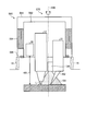
2 三次元積層室
3 予備室
4 積層ヘッド収納室
4a、5a Z軸スライド部
5 機械加工部収納室
6、7 扉
10 ベッド
11 テーブル部
12 積層ヘッド
13 機械加工部
15 Y軸スライド部
16 X軸スライド部
17 回転テーブル部
18、19 ベローズ
20 制御装置
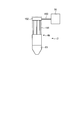
22 工具
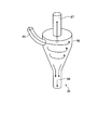
23 ノズル
24 先端部
25 空気排出部
30 形状計測部
31、31a 加熱ヘッド
32 機械加工部計測部
33 工具交換部
34 ノズル交換部
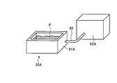
35、35A 粉末導入部
36 基台移動部
37 空気排出部
38 ガス導入部
39 粉末回収部
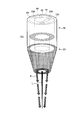
41 外管
42 内管
43 粉末流路
44 レーザ経路
46 本体
47 光源
48 光ファイバ
49 集光部
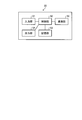
51 入力部
52 制御部
53 記憶部
54 出力部
55 通信部
56 先端
57 光源部
58 撮像部
81、81A 粉末収納部
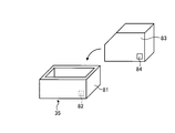
82、82A 粉末識別部
83 カートリッジ
84 材料表示部
85 導入部
86 サイクロン部
87 気体排出部
88 粉末排出部
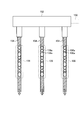
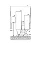
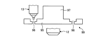
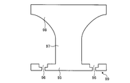
91 台座
92、93 成形層
95 円板部
96 ねじ穴部
97 軸部
98 円錐台部
99 部材
100 基台部
102、104、106、108 矢印
110、112、114 回転軸
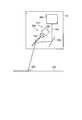
120、120a 温度検出部
130 質量検出部
140 焦点位置調整部
150 粉末供給管
152 分配部
154 分岐管
156 混合部
156a 撹拌板
158 整流装置
162 レーザ光
164 測定波
182 ハーフミラー
190 プラズマ発光検出部
192 反射光検出部
502、502a 光源ユニット
504、504a 加熱位置調整機構
512、520、560 ミラー
512a、514 ガルバノミラー
522、562 角度位置調整機構
532 領域
540、540a 半導体レーザ
542 集光部
544 光ファイバ
550 合波部
551 コリメートレンズ
552 回折格子
554 集光部
A 溶融体
B 固化体
L レーザ光
P 粉末
P1、P2 焦点位置 DESCRIPTION OF SYMBOLS 1 3D laminating apparatus 2 3D laminating room 3 Preliminary room 4 Laminating head storage room 4a, 5a Z axis slide part 5 Machining part storage room 6, 7 Door 10 Bed 11 Table part 12 Laminating head 13 Machining part 15 Y axis Slide part 16 X-axis slide part 17 Rotary table part 18, 19 Bellows 20 Control device 22 Tool 23 Nozzle 24 Tip part 25 Air discharge part 30 Shape measurement part 31, 31a Heating head 32 Machining part measurement part 33 Tool exchange part 34 Nozzle Exchanger 35, 35A Powder introduction part 36 Base movement part 37 Air discharge part 38 Gas introduction part 39 Powder recovery part 41 Outer pipe 42 Inner pipe 43 Powder flow path 44 Laser path 46 Main body 47 Light source 48 Optical fiber 49 Condensing part 51 Input unit 52 Control unit 53 Storage unit 54 Output unit 55 Communication unit 56 Tip 57 Light source unit 58 Imaging Part 81, 81A Powder storage part 82, 82A Powder identification part 83 Cartridge 84 Material display part 85 Introduction part 86 Cyclone part 87 Gas discharge part 88 Powder discharge part 91 Base 92, 93 Molding layer 95 Disc part 96 Screw hole part 97 Shaft Part 98 Frustum part 99 Member 100 Base part 102, 104, 106, 108 Arrows 110, 112, 114 Rotating shaft 120, 120a Temperature detection part 130 Mass detection part 140 Focal position adjustment part 150 Powder supply pipe 152 Distribution part 154 Branch Tube 156 Mixing unit 156a Stirring plate 158 Rectifier 162 Laser beam 164 Measurement wave 182 Half mirror 190 Plasma emission detecting unit 192 Reflected light detecting unit 502, 502a Light source unit 504, 504a Heating position adjusting mechanism 512, 520, 560 Mirror 512a, 514 Galvano mirror 522, 62 angular position adjusting mechanism 532 regions 540,540a semiconductor laser 542 light collecting unit 544 optical fiber 550 multiplexing unit 551 554 condensing unit collimator lens 552 diffraction grating A melt B solidified L laser beam P powder P1, P2 focal position
Claims (19)
- 基台部に成形層を積層させて三次元形状を形成する三次元積層装置であって、
粉末材料を供給する粉末供給部と、
前記粉末材料に光ビームを照射し、前記光ビームが照射された前記粉末材料の少なくとも一部を焼結又は溶融固化させて前記成形層を形成する光照射部と、
前記基台部または成形層の前記光ビームが照射される位置を通過した領域または前記光ビームが照射される位置を通過する前の領域を選択的に加熱する加熱部と、
前記粉末供給部、前記光照射部及び前記加熱部の動作を制御する制御装置と、を有する三次元積層装置。 A three-dimensional laminating apparatus that forms a three-dimensional shape by laminating a molding layer on a base part,
A powder supply unit for supplying powder material;
A light irradiation part for irradiating the powder material with a light beam, and sintering or melting and solidifying at least a part of the powder material irradiated with the light beam;
A heating unit that selectively heats a region of the base part or the molding layer that has passed through the position irradiated with the light beam or a region before passing through the position irradiated with the light beam;
A three-dimensional laminating apparatus comprising: a control device that controls operations of the powder supply unit, the light irradiation unit, and the heating unit. - 前記粉末供給部は、前記基台部に向かって前記粉末材料を噴射し、
前記光照射部は、前記粉末供給部から前記基台部に向けて移動する前記粉末材料に光ビームを照射し、前記粉末材料を溶融させて、溶融した前記粉末材料を前記基台部上で固化させて前記成形層を形成する請求項1に記載の三次元積層装置。 The powder supply unit injects the powder material toward the base unit,
The light irradiation unit irradiates the powder material moving from the powder supply unit toward the base unit with a light beam, melts the powder material, and causes the powder material to melt on the base unit. The three-dimensional laminating apparatus according to claim 1, wherein the molding layer is formed by solidification. - 前記粉末供給部は、前記光照射部の外周に同心円状に配置され、前記光照射部の前記光ビームが通過する経路を囲う内管と前記内管を覆う外管との間が前記粉末材料の流れる粉末流路となる請求項2に記載の三次元積層装置。 The powder supply unit is concentrically arranged on the outer periphery of the light irradiation unit, and the powder material is between an inner tube that surrounds a path through which the light beam of the light irradiation unit passes and an outer tube that covers the inner tube. The three-dimensional laminating apparatus according to claim 2, wherein the three-dimensional laminating apparatus is a powder flow path through which the gas flows.
- 前記光照射部及び前記粉末供給部と、前記基台部と、を相対移動させる移動機構を有し、
前記制御装置は、前記移動機構によって前記基台部に対して前記光照射部及び前記粉末供給部が通過する経路を決定する請求項2または3に記載の三次元積層装置。 A moving mechanism for relatively moving the light irradiation unit, the powder supply unit, and the base unit;
The said control apparatus is a three-dimensional laminating apparatus of Claim 2 or 3 which determines the path | route through which the said light irradiation part and the said powder supply part pass with respect to the said base part by the said moving mechanism. - 前記加熱部は、光ビームを出力する光源ユニットを有し、
前記光源ユニットから出力する光ビームを照射して加熱を行う請求項1から4のいずれか一項に記載の三次元積層装置。 The heating unit includes a light source unit that outputs a light beam,
The three-dimensional laminating apparatus according to any one of claims 1 to 4, wherein heating is performed by irradiating a light beam output from the light source unit. - 前記光ビームは、レーザ光である請求項5に記載の三次元積層装置。 The three-dimensional stacking apparatus according to claim 5, wherein the light beam is a laser beam.
- 前記加熱部は、前記光源ユニットから出力された光ビームを反射するミラー及び前記ミラーの角度を調整する角度調整機構を備える照射位置調整機構を備える請求項5または6に記載の三次元積層装置。 The three-dimensional laminating apparatus according to claim 5 or 6, wherein the heating unit includes an irradiation position adjustment mechanism including a mirror that reflects a light beam output from the light source unit and an angle adjustment mechanism that adjusts an angle of the mirror.
- 前記光源ユニットは、レーザ光を出力する半導体レーザと、前記半導体レーザから出力されたレーザ光を集光する集光部と、前記集光部で集光されたレーザ光が入射される光ファイバとを有する請求項5から7のいずれか一項に記載の三次元積層装置。 The light source unit includes a semiconductor laser that outputs laser light, a condensing unit that condenses the laser light output from the semiconductor laser, and an optical fiber into which the laser light collected by the condensing unit is incident. The three-dimensional laminating apparatus according to any one of claims 5 to 7, comprising:
- 前記光源ユニットは、前記半導体レーザと前記集光部とを複数有し、
複数の前記半導体レーザで出力され、それぞれの前記集光部で集光されたレーザ光が1つの光ファイバに入射される請求項8に記載の三次元積層装置。 The light source unit includes a plurality of the semiconductor lasers and the condensing unit,
The three-dimensional laminating apparatus according to claim 8, wherein laser beams output from a plurality of the semiconductor lasers and condensed by the respective condensing units are incident on one optical fiber. - 前記半導体レーザは、垂直発光型半導体レーザである請求項8に記載の三次元積層装置。 The three-dimensional laminating apparatus according to claim 8, wherein the semiconductor laser is a vertical light emitting semiconductor laser.
- 前記半導体レーザを複数有し、
前記集光部は、複数の前記半導体レーザのそれぞれに配置されたコリメートレンズと、
複数の前記コリメートレンズでコリメートされたレーザ光を合波して前記光ファイバに入射させる合波部と、を有する請求項10に記載の三次元積層装置。 A plurality of the semiconductor lasers;
The condensing unit includes a collimating lens disposed in each of the plurality of semiconductor lasers,
The three-dimensional laminating apparatus according to claim 10, further comprising: a multiplexing unit configured to multiplex laser beams collimated by the plurality of collimating lenses and to enter the optical fiber. - 前記成形層の表面の温度と分布を検出する温度検出部を有し、
前記制御装置は、前記温度検出部による前記成形層の表面温度の計測結果に応じて、前記加熱部による加熱を制御する請求項1から11のいずれか一項に記載の三次元積層装置。 A temperature detection unit for detecting the temperature and distribution of the surface of the molding layer;
The three-dimensional laminating apparatus according to any one of claims 1 to 11, wherein the control device controls heating by the heating unit in accordance with a measurement result of a surface temperature of the molding layer by the temperature detection unit. - 前記制御装置は、前記温度検出部による前記成形層の表面温度の計測結果と、前記基台部及び前記成形層の特性とに基づいて、前記加熱部による加熱を制御する請求項12に記載の三次元積層装置。 The said control apparatus of Claim 12 which controls the heating by the said heating part based on the measurement result of the surface temperature of the said shaping | molding layer by the said temperature detection part, and the characteristic of the said base part and the said shaping | molding layer. Three-dimensional laminating device.
- 前記成形層の表面のプラズマ発光を検出するプラズマ発光検出部を有し、
前記制御装置は、前記プラズマ発光検出部による計測結果に応じて、前記加熱部による加熱を制御する請求項1から13のいずれか一項に記載の三次元積層装置。 Having a plasma emission detector for detecting plasma emission on the surface of the molding layer;
The three-dimensional laminating apparatus according to any one of claims 1 to 13, wherein the control device controls heating by the heating unit in accordance with a measurement result by the plasma light emission detection unit. - 前記成形層の表面からの反射光を検出する反射光検出部を有し、
前記制御装置は、前記反射光検出部による計測結果に応じて、前記加熱部による加熱を制御する請求項1から14のいずれか一項に記載の三次元積層装置。 A reflected light detection unit for detecting reflected light from the surface of the molding layer;
The three-dimensional laminating apparatus according to any one of claims 1 to 14, wherein the control device controls heating by the heating unit in accordance with a measurement result by the reflected light detection unit. - 前記加熱部は、前記光ビームが照射される位置を通過した領域を加熱する請求項1から15のいずれか一項に記載の三次元積層装置。 The three-dimensional laminating apparatus according to any one of claims 1 to 15, wherein the heating unit heats a region that has passed a position irradiated with the light beam.
- 前記加熱部は、前記光ビームが照射される位置を通過する前の領域を加熱する請求項1から15のいずれか一項に記載の三次元積層装置。 The three-dimensional laminating apparatus according to any one of claims 1 to 15, wherein the heating unit heats a region before passing through a position irradiated with the light beam.
- 前記光照射部と前記加熱部の相対位置を切り換える切換機構を有し、
前記制御装置は、前記光照射部と前記加熱部と、前記基台部との相対移動の方向と、前記加熱部で加熱する領域が、前記基台部または成形層の前記光ビームが照射される位置を通過した領域であるか前記光ビームが照射される位置を通過する前の領域であるかに応じて、前記切換機構により前記光照射部と前記加熱部の相対位置を制御する請求項1から15のいずれか一項に記載の三次元積層装置。 A switching mechanism for switching a relative position between the light irradiation unit and the heating unit;
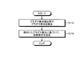
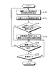
The control device is configured to irradiate the light beam of the base part or the molding layer in a direction of relative movement between the light irradiation part, the heating part, and the base part, and a region heated by the heating part. The relative position of the light irradiation unit and the heating unit is controlled by the switching mechanism according to whether the region passes through a position where the light beam is irradiated or the region before passing through the position irradiated with the light beam. The three-dimensional laminating apparatus as described in any one of 1 to 15. - 基台部に成形層を積層して三次元形状物を形成する三次元積層方法であって、
粉末材料を基台部に向かって噴射しつつ、前記粉末材料に光ビームを照射することにより前記粉末材料を溶融させ、前記溶融した粉末材料を前記基台部上で固化させることにより前記基台部上に成形層を形成し、当該成形層を積層する積層ステップと、
前記基台部または成形層の前記光ビームが照射される位置を通過した領域または前記光ビームが照射される位置を通過する前の領域に光ビームを照射し選択的に加熱するステップと、を有する三次元積層方法。 A three-dimensional lamination method of forming a three-dimensional shape by laminating a molding layer on a base part,
The base material is melted by irradiating the powder material with a light beam while spraying the powder material toward the base portion, and the molten powder material is solidified on the base portion. Forming a molding layer on the part and laminating the molding layer; and
Irradiating and selectively heating the region of the base part or the molding layer that has passed through the position irradiated with the light beam or the region before passing through the position irradiated with the light beam; and A three-dimensional stacking method.
Priority Applications (6)
| Application Number | Priority Date | Filing Date | Title |
|---|---|---|---|
| CN201580017061.1A CN106163703B (en) | 2014-03-31 | 2015-03-20 | Three-dimensional laminating apparatus and three-dimensional laminating method |
| KR1020187012290A KR20180049219A (en) | 2014-03-31 | 2015-03-20 | Three-dimensional lamination device and three-dimensional lamination method |
| EP15773604.2A EP3127685B1 (en) | 2014-03-31 | 2015-03-20 | Three-dimensional deposition device and three-dimensional deposition method |
| US15/129,923 US10898971B2 (en) | 2014-03-31 | 2015-03-20 | Three-dimensional deposition device and three-dimensional deposition method |
| KR1020167027064A KR20160129871A (en) | 2014-03-31 | 2015-03-20 | Three-dimensional lamination device and three-dimensional lamination method |
| MX2016012702A MX2016012702A (en) | 2014-03-31 | 2015-03-20 | Three-dimensional lamination device and three-dimensional lamination method. |
Applications Claiming Priority (2)
| Application Number | Priority Date | Filing Date | Title |
|---|---|---|---|
| JP2014-074058 | 2014-03-31 | ||
| JP2014074058A JP6254036B2 (en) | 2014-03-31 | 2014-03-31 | Three-dimensional laminating apparatus and three-dimensional laminating method |
Publications (1)
| Publication Number | Publication Date |
|---|---|
| WO2015151864A1 true WO2015151864A1 (en) | 2015-10-08 |
Family
ID=54240194
Family Applications (1)
| Application Number | Title | Priority Date | Filing Date |
|---|---|---|---|
| PCT/JP2015/058496 WO2015151864A1 (en) | 2014-03-31 | 2015-03-20 | Three-dimensional lamination device and three-dimensional lamination method |
Country Status (8)
| Country | Link |
|---|---|
| US (1) | US10898971B2 (en) |
| EP (1) | EP3127685B1 (en) |
| JP (1) | JP6254036B2 (en) |
| KR (2) | KR20180049219A (en) |
| CN (1) | CN106163703B (en) |
| MX (1) | MX2016012702A (en) |
| TW (1) | TWI600485B (en) |
| WO (1) | WO2015151864A1 (en) |
Cited By (7)
| Publication number | Priority date | Publication date | Assignee | Title |
|---|---|---|---|---|
| CN107042306A (en) * | 2016-02-09 | 2017-08-15 | 株式会社捷太格特 | The manufacture device and manufacture method of moulder |
| DE102016120044A1 (en) * | 2016-10-20 | 2018-04-26 | Cl Schutzrechtsverwaltungs Gmbh | Device for the additive production of three-dimensional objects |
| US10479018B2 (en) | 2015-03-30 | 2019-11-19 | Renishaw Plc | Additive manufacturing apparatus and methods |
| EP3372061A4 (en) * | 2015-11-06 | 2019-11-27 | IPG Photonics Corporation | Modular laser processing enclosure and system |
| WO2020261386A1 (en) * | 2019-06-25 | 2020-12-30 | 三菱電機株式会社 | Numerical control device and method for controlling additional manufacturing device |
| US11123799B2 (en) | 2013-06-11 | 2021-09-21 | Renishaw Plc | Additive manufacturing apparatus and method |
| US11478856B2 (en) | 2013-06-10 | 2022-10-25 | Renishaw Plc | Selective laser solidification apparatus and method |
Families Citing this family (341)
| Publication number | Priority date | Publication date | Assignee | Title |
|---|---|---|---|---|
| US10378106B2 (en) | 2008-11-14 | 2019-08-13 | Asm Ip Holding B.V. | Method of forming insulation film by modified PEALD |
| US9394608B2 (en) | 2009-04-06 | 2016-07-19 | Asm America, Inc. | Semiconductor processing reactor and components thereof |
| US8802201B2 (en) | 2009-08-14 | 2014-08-12 | Asm America, Inc. | Systems and methods for thin-film deposition of metal oxides using excited nitrogen-oxygen species |
| US9312155B2 (en) | 2011-06-06 | 2016-04-12 | Asm Japan K.K. | High-throughput semiconductor-processing apparatus equipped with multiple dual-chamber modules |
| US10364496B2 (en) | 2011-06-27 | 2019-07-30 | Asm Ip Holding B.V. | Dual section module having shared and unshared mass flow controllers |
| US10854498B2 (en) | 2011-07-15 | 2020-12-01 | Asm Ip Holding B.V. | Wafer-supporting device and method for producing same |
| US20130023129A1 (en) | 2011-07-20 | 2013-01-24 | Asm America, Inc. | Pressure transmitter for a semiconductor processing environment |
| US9017481B1 (en) | 2011-10-28 | 2015-04-28 | Asm America, Inc. | Process feed management for semiconductor substrate processing |
| US9659799B2 (en) | 2012-08-28 | 2017-05-23 | Asm Ip Holding B.V. | Systems and methods for dynamic semiconductor process scheduling |
| US9021985B2 (en) | 2012-09-12 | 2015-05-05 | Asm Ip Holdings B.V. | Process gas management for an inductively-coupled plasma deposition reactor |
| US10714315B2 (en) | 2012-10-12 | 2020-07-14 | Asm Ip Holdings B.V. | Semiconductor reaction chamber showerhead |
| US20160376700A1 (en) | 2013-02-01 | 2016-12-29 | Asm Ip Holding B.V. | System for treatment of deposition reactor |
| US9589770B2 (en) | 2013-03-08 | 2017-03-07 | Asm Ip Holding B.V. | Method and systems for in-situ formation of intermediate reactive species |
| US9484191B2 (en) | 2013-03-08 | 2016-11-01 | Asm Ip Holding B.V. | Pulsed remote plasma method and system |
| US9240412B2 (en) | 2013-09-27 | 2016-01-19 | Asm Ip Holding B.V. | Semiconductor structure and device and methods of forming same using selective epitaxial process |
| US10683571B2 (en) | 2014-02-25 | 2020-06-16 | Asm Ip Holding B.V. | Gas supply manifold and method of supplying gases to chamber using same |
| US10167557B2 (en) | 2014-03-18 | 2019-01-01 | Asm Ip Holding B.V. | Gas distribution system, reactor including the system, and methods of using the same |
| US11015245B2 (en) | 2014-03-19 | 2021-05-25 | Asm Ip Holding B.V. | Gas-phase reactor and system having exhaust plenum and components thereof |
| JP6359316B2 (en) | 2014-03-31 | 2018-07-18 | 三菱重工業株式会社 | Three-dimensional laminating apparatus and three-dimensional laminating method |
| US10618131B2 (en) | 2014-06-05 | 2020-04-14 | Nlight, Inc. | Laser patterning skew correction |
| US10858737B2 (en) | 2014-07-28 | 2020-12-08 | Asm Ip Holding B.V. | Showerhead assembly and components thereof |
| US9890456B2 (en) | 2014-08-21 | 2018-02-13 | Asm Ip Holding B.V. | Method and system for in situ formation of gas-phase compounds |
| US10941490B2 (en) | 2014-10-07 | 2021-03-09 | Asm Ip Holding B.V. | Multiple temperature range susceptor, assembly, reactor and system including the susceptor, and methods of using the same |
| US9657845B2 (en) | 2014-10-07 | 2017-05-23 | Asm Ip Holding B.V. | Variable conductance gas distribution apparatus and method |
| KR102263121B1 (en) | 2014-12-22 | 2021-06-09 | 에이에스엠 아이피 홀딩 비.브이. | Semiconductor device and manufacuring method thereof |
| US10529542B2 (en) | 2015-03-11 | 2020-01-07 | Asm Ip Holdings B.V. | Cross-flow reactor and method |
| US10276355B2 (en) | 2015-03-12 | 2019-04-30 | Asm Ip Holding B.V. | Multi-zone reactor, system including the reactor, and method of using the same |
| US10458018B2 (en) | 2015-06-26 | 2019-10-29 | Asm Ip Holding B.V. | Structures including metal carbide material, devices including the structures, and methods of forming same |
| US10600673B2 (en) | 2015-07-07 | 2020-03-24 | Asm Ip Holding B.V. | Magnetic susceptor to baseplate seal |
| US10083836B2 (en) | 2015-07-24 | 2018-09-25 | Asm Ip Holding B.V. | Formation of boron-doped titanium metal films with high work function |
| US9960072B2 (en) | 2015-09-29 | 2018-05-01 | Asm Ip Holding B.V. | Variable adjustment for precise matching of multiple chamber cavity housings |
| US10211308B2 (en) | 2015-10-21 | 2019-02-19 | Asm Ip Holding B.V. | NbMC layers |
| US10322384B2 (en) | 2015-11-09 | 2019-06-18 | Asm Ip Holding B.V. | Counter flow mixer for process chamber |
| US11179807B2 (en) | 2015-11-23 | 2021-11-23 | Nlight, Inc. | Fine-scale temporal control for laser material processing |
| CN108367389B (en) | 2015-11-23 | 2020-07-28 | 恩耐公司 | Laser processing method and apparatus |
| US10688596B2 (en) * | 2015-12-18 | 2020-06-23 | Illinois Tool Works Inc. | Wire manufactured by additive manufacturing methods |
| US11139308B2 (en) | 2015-12-29 | 2021-10-05 | Asm Ip Holding B.V. | Atomic layer deposition of III-V compounds to form V-NAND devices |
| FR3046367A1 (en) * | 2015-12-31 | 2017-07-07 | Nantes Ecole Centrale | DEVICE FOR ADDITIVE MANUFACTURING BY PROJECTION AND POWDER FUSION |
| US10468251B2 (en) | 2016-02-19 | 2019-11-05 | Asm Ip Holding B.V. | Method for forming spacers using silicon nitride film for spacer-defined multiple patterning |
| US10529554B2 (en) | 2016-02-19 | 2020-01-07 | Asm Ip Holding B.V. | Method for forming silicon nitride film selectively on sidewalls or flat surfaces of trenches |
| US10831180B2 (en) * | 2016-02-25 | 2020-11-10 | General Electric Company | Multivariate statistical process control of laser powder bed additive manufacturing |
| US10501866B2 (en) | 2016-03-09 | 2019-12-10 | Asm Ip Holding B.V. | Gas distribution apparatus for improved film uniformity in an epitaxial system |
| US10343920B2 (en) | 2016-03-18 | 2019-07-09 | Asm Ip Holding B.V. | Aligned carbon nanotubes |
| US9892913B2 (en) | 2016-03-24 | 2018-02-13 | Asm Ip Holding B.V. | Radial and thickness control via biased multi-port injection settings |
| US20180162053A1 (en) * | 2016-03-25 | 2018-06-14 | Technology Research Association For Future Additive Manufacturing | Three-dimensional laminating and shaping apparatus, control method of three-dimensional laminating and shaping apparatus, and control program of three-dimensional laminating and shaping apparatus |
| US10865475B2 (en) | 2016-04-21 | 2020-12-15 | Asm Ip Holding B.V. | Deposition of metal borides and silicides |
| US10190213B2 (en) | 2016-04-21 | 2019-01-29 | Asm Ip Holding B.V. | Deposition of metal borides |
| US10032628B2 (en) | 2016-05-02 | 2018-07-24 | Asm Ip Holding B.V. | Source/drain performance through conformal solid state doping |
| US10367080B2 (en) | 2016-05-02 | 2019-07-30 | Asm Ip Holding B.V. | Method of forming a germanium oxynitride film |
| KR102592471B1 (en) | 2016-05-17 | 2023-10-20 | 에이에스엠 아이피 홀딩 비.브이. | Method of forming metal interconnection and method of fabricating semiconductor device using the same |
| US11453943B2 (en) | 2016-05-25 | 2022-09-27 | Asm Ip Holding B.V. | Method for forming carbon-containing silicon/metal oxide or nitride film by ALD using silicon precursor and hydrocarbon precursor |
| DE102016210042B3 (en) | 2016-06-07 | 2017-10-19 | Sauer Gmbh | Machine tool for build-up welding |
| KR101787718B1 (en) * | 2016-06-21 | 2017-11-16 | 한국기계연구원 | 3-dimensional laser printing apparatus and method |
| US10388509B2 (en) | 2016-06-28 | 2019-08-20 | Asm Ip Holding B.V. | Formation of epitaxial layers via dislocation filtering |
| US10612137B2 (en) | 2016-07-08 | 2020-04-07 | Asm Ip Holdings B.V. | Organic reactants for atomic layer deposition |
| US9859151B1 (en) | 2016-07-08 | 2018-01-02 | Asm Ip Holding B.V. | Selective film deposition method to form air gaps |
| US10714385B2 (en) | 2016-07-19 | 2020-07-14 | Asm Ip Holding B.V. | Selective deposition of tungsten |
| KR102354490B1 (en) | 2016-07-27 | 2022-01-21 | 에이에스엠 아이피 홀딩 비.브이. | Method of processing a substrate |
| US9887082B1 (en) | 2016-07-28 | 2018-02-06 | Asm Ip Holding B.V. | Method and apparatus for filling a gap |
| KR102532607B1 (en) | 2016-07-28 | 2023-05-15 | 에이에스엠 아이피 홀딩 비.브이. | Substrate processing apparatus and method of operating the same |
| US10395919B2 (en) | 2016-07-28 | 2019-08-27 | Asm Ip Holding B.V. | Method and apparatus for filling a gap |
| US9812320B1 (en) | 2016-07-28 | 2017-11-07 | Asm Ip Holding B.V. | Method and apparatus for filling a gap |
| CN109791252B (en) | 2016-09-29 | 2021-06-29 | 恩耐公司 | Adjustable beam characteristics |
| TWI633994B (en) * | 2016-10-06 | 2018-09-01 | 國立中興大學 | 3D printing device capable of instantly monitoring temperature and temperature monitoring method thereof |
| US10410943B2 (en) | 2016-10-13 | 2019-09-10 | Asm Ip Holding B.V. | Method for passivating a surface of a semiconductor and related systems |
| US10643826B2 (en) | 2016-10-26 | 2020-05-05 | Asm Ip Holdings B.V. | Methods for thermally calibrating reaction chambers |
| US11532757B2 (en) | 2016-10-27 | 2022-12-20 | Asm Ip Holding B.V. | Deposition of charge trapping layers |
| US10643904B2 (en) | 2016-11-01 | 2020-05-05 | Asm Ip Holdings B.V. | Methods for forming a semiconductor device and related semiconductor device structures |
| US10435790B2 (en) | 2016-11-01 | 2019-10-08 | Asm Ip Holding B.V. | Method of subatmospheric plasma-enhanced ALD using capacitively coupled electrodes with narrow gap |
| US10714350B2 (en) | 2016-11-01 | 2020-07-14 | ASM IP Holdings, B.V. | Methods for forming a transition metal niobium nitride film on a substrate by atomic layer deposition and related semiconductor device structures |
| US10229833B2 (en) | 2016-11-01 | 2019-03-12 | Asm Ip Holding B.V. | Methods for forming a transition metal nitride film on a substrate by atomic layer deposition and related semiconductor device structures |
| US10134757B2 (en) | 2016-11-07 | 2018-11-20 | Asm Ip Holding B.V. | Method of processing a substrate and a device manufactured by using the method |
| KR102546317B1 (en) | 2016-11-15 | 2023-06-21 | 에이에스엠 아이피 홀딩 비.브이. | Gas supply unit and substrate processing apparatus including the same |
| US10340135B2 (en) | 2016-11-28 | 2019-07-02 | Asm Ip Holding B.V. | Method of topologically restricted plasma-enhanced cyclic deposition of silicon or metal nitride |
| KR20180068582A (en) | 2016-12-14 | 2018-06-22 | 에이에스엠 아이피 홀딩 비.브이. | Substrate processing apparatus |
| US11447861B2 (en) | 2016-12-15 | 2022-09-20 | Asm Ip Holding B.V. | Sequential infiltration synthesis apparatus and a method of forming a patterned structure |
| US11581186B2 (en) | 2016-12-15 | 2023-02-14 | Asm Ip Holding B.V. | Sequential infiltration synthesis apparatus |
| KR20180070971A (en) | 2016-12-19 | 2018-06-27 | 에이에스엠 아이피 홀딩 비.브이. | Substrate processing apparatus |
| US10269558B2 (en) | 2016-12-22 | 2019-04-23 | Asm Ip Holding B.V. | Method of forming a structure on a substrate |
| JP6856238B2 (en) * | 2016-12-27 | 2021-04-07 | 白光株式会社 | Manufacturing method of tip member of heating tool |
| US10867788B2 (en) | 2016-12-28 | 2020-12-15 | Asm Ip Holding B.V. | Method of forming a structure on a substrate |
| US10821512B2 (en) * | 2017-01-06 | 2020-11-03 | General Electric Company | Systems and methods for controlling microstructure of additively manufactured components |
| US10655221B2 (en) | 2017-02-09 | 2020-05-19 | Asm Ip Holding B.V. | Method for depositing oxide film by thermal ALD and PEALD |
| US10468261B2 (en) | 2017-02-15 | 2019-11-05 | Asm Ip Holding B.V. | Methods for forming a metallic film on a substrate by cyclical deposition and related semiconductor device structures |
| US10283353B2 (en) | 2017-03-29 | 2019-05-07 | Asm Ip Holding B.V. | Method of reforming insulating film deposited on substrate with recess pattern |
| US10529563B2 (en) | 2017-03-29 | 2020-01-07 | Asm Ip Holdings B.V. | Method for forming doped metal oxide films on a substrate by cyclical deposition and related semiconductor device structures |
| WO2018181334A1 (en) * | 2017-03-31 | 2018-10-04 | 株式会社ニコン | Modeling system and modeling method |
| US10103040B1 (en) * | 2017-03-31 | 2018-10-16 | Asm Ip Holding B.V. | Apparatus and method for manufacturing a semiconductor device |
| WO2018187489A1 (en) * | 2017-04-04 | 2018-10-11 | Nlight, Inc. | Optical fiducial generation for galvanometric scanner calibration |
| JP6626036B2 (en) * | 2017-04-18 | 2019-12-25 | ファナック株式会社 | Laser processing system with measurement function |
| KR102457289B1 (en) | 2017-04-25 | 2022-10-21 | 에이에스엠 아이피 홀딩 비.브이. | Method for depositing a thin film and manufacturing a semiconductor device |
| CN107415239A (en) * | 2017-05-05 | 2017-12-01 | 南通理工学院 | A kind of UV photocurings 3D rapid prototyping systems and its Method of printing |
| US10770286B2 (en) | 2017-05-08 | 2020-09-08 | Asm Ip Holdings B.V. | Methods for selectively forming a silicon nitride film on a substrate and related semiconductor device structures |
| US10446393B2 (en) | 2017-05-08 | 2019-10-15 | Asm Ip Holding B.V. | Methods for forming silicon-containing epitaxial layers and related semiconductor device structures |
| US10892156B2 (en) | 2017-05-08 | 2021-01-12 | Asm Ip Holding B.V. | Methods for forming a silicon nitride film on a substrate and related semiconductor device structures |
| KR101974722B1 (en) * | 2017-05-26 | 2019-05-02 | 전북대학교산학협력단 | Device for real-time quality monitoring and quality control for three dimensional additive manufacturing process and the method for the same |
| US10504742B2 (en) | 2017-05-31 | 2019-12-10 | Asm Ip Holding B.V. | Method of atomic layer etching using hydrogen plasma |
| US10886123B2 (en) | 2017-06-02 | 2021-01-05 | Asm Ip Holding B.V. | Methods for forming low temperature semiconductor layers and related semiconductor device structures |
| JP6289713B1 (en) * | 2017-06-12 | 2018-03-07 | 南海鋼材株式会社 | Welding system and welding method |
| US11306395B2 (en) | 2017-06-28 | 2022-04-19 | Asm Ip Holding B.V. | Methods for depositing a transition metal nitride film on a substrate by atomic layer deposition and related deposition apparatus |
| US10685834B2 (en) | 2017-07-05 | 2020-06-16 | Asm Ip Holdings B.V. | Methods for forming a silicon germanium tin layer and related semiconductor device structures |
| KR20190009245A (en) | 2017-07-18 | 2019-01-28 | 에이에스엠 아이피 홀딩 비.브이. | Methods for forming a semiconductor device structure and related semiconductor device structures |
| US11018002B2 (en) | 2017-07-19 | 2021-05-25 | Asm Ip Holding B.V. | Method for selectively depositing a Group IV semiconductor and related semiconductor device structures |
| US11374112B2 (en) | 2017-07-19 | 2022-06-28 | Asm Ip Holding B.V. | Method for depositing a group IV semiconductor and related semiconductor device structures |
| US10541333B2 (en) | 2017-07-19 | 2020-01-21 | Asm Ip Holding B.V. | Method for depositing a group IV semiconductor and related semiconductor device structures |
| US10590535B2 (en) | 2017-07-26 | 2020-03-17 | Asm Ip Holdings B.V. | Chemical treatment, deposition and/or infiltration apparatus and method for using the same |
| US10605530B2 (en) | 2017-07-26 | 2020-03-31 | Asm Ip Holding B.V. | Assembly of a liner and a flange for a vertical furnace as well as the liner and the vertical furnace |
| US10312055B2 (en) | 2017-07-26 | 2019-06-04 | Asm Ip Holding B.V. | Method of depositing film by PEALD using negative bias |
| CN109366981B (en) * | 2017-08-03 | 2021-06-11 | 株式会社松浦机械制作所 | Method for three-dimensional object modeling |
| DE102017213720A1 (en) * | 2017-08-07 | 2019-02-07 | Eos Gmbh Electro Optical Systems | Optimized segmentation process |
| US10692741B2 (en) | 2017-08-08 | 2020-06-23 | Asm Ip Holdings B.V. | Radiation shield |
| US10770336B2 (en) | 2017-08-08 | 2020-09-08 | Asm Ip Holding B.V. | Substrate lift mechanism and reactor including same |
| US11139191B2 (en) | 2017-08-09 | 2021-10-05 | Asm Ip Holding B.V. | Storage apparatus for storing cassettes for substrates and processing apparatus equipped therewith |
| US11769682B2 (en) | 2017-08-09 | 2023-09-26 | Asm Ip Holding B.V. | Storage apparatus for storing cassettes for substrates and processing apparatus equipped therewith |
| US10249524B2 (en) | 2017-08-09 | 2019-04-02 | Asm Ip Holding B.V. | Cassette holder assembly for a substrate cassette and holding member for use in such assembly |
| US10236177B1 (en) | 2017-08-22 | 2019-03-19 | ASM IP Holding B.V.. | Methods for depositing a doped germanium tin semiconductor and related semiconductor device structures |
| USD900036S1 (en) | 2017-08-24 | 2020-10-27 | Asm Ip Holding B.V. | Heater electrical connector and adapter |
| US11830730B2 (en) | 2017-08-29 | 2023-11-28 | Asm Ip Holding B.V. | Layer forming method and apparatus |
| KR102491945B1 (en) | 2017-08-30 | 2023-01-26 | 에이에스엠 아이피 홀딩 비.브이. | Substrate processing apparatus |
| US11056344B2 (en) | 2017-08-30 | 2021-07-06 | Asm Ip Holding B.V. | Layer forming method |
| US11295980B2 (en) | 2017-08-30 | 2022-04-05 | Asm Ip Holding B.V. | Methods for depositing a molybdenum metal film over a dielectric surface of a substrate by a cyclical deposition process and related semiconductor device structures |
| JP6393873B1 (en) * | 2017-09-05 | 2018-09-26 | 株式会社松浦機械製作所 | 3D modeling equipment |
| DE102017215838A1 (en) | 2017-09-07 | 2019-03-07 | Sauer Gmbh | Replaceable optics module for a laser processing machine |
| DE102017215840A1 (en) | 2017-09-07 | 2019-03-07 | Sauer Gmbh | Replaceable focusing module |
| DE102017215841A1 (en) | 2017-09-07 | 2019-03-07 | Sauer Gmbh | Powder nozzle for a laser processing machine |
| DE102017215839A1 (en) | 2017-09-07 | 2019-03-07 | Sauer Gmbh | Optics module with device for automatically changing a collimation optics |
| US10607895B2 (en) | 2017-09-18 | 2020-03-31 | Asm Ip Holdings B.V. | Method for forming a semiconductor device structure comprising a gate fill metal |
| KR102630301B1 (en) | 2017-09-21 | 2024-01-29 | 에이에스엠 아이피 홀딩 비.브이. | Method of sequential infiltration synthesis treatment of infiltrateable material and structures and devices formed using same |
| US10844484B2 (en) | 2017-09-22 | 2020-11-24 | Asm Ip Holding B.V. | Apparatus for dispensing a vapor phase reactant to a reaction chamber and related methods |
| US10658205B2 (en) | 2017-09-28 | 2020-05-19 | Asm Ip Holdings B.V. | Chemical dispensing apparatus and methods for dispensing a chemical to a reaction chamber |
| US10403504B2 (en) | 2017-10-05 | 2019-09-03 | Asm Ip Holding B.V. | Method for selectively depositing a metallic film on a substrate |
| US11554442B2 (en) * | 2017-10-06 | 2023-01-17 | Ihi Corporation | Additive manufacturing device and additive manufacturing method |
| JP6577110B2 (en) * | 2017-10-06 | 2019-09-18 | 株式会社アマダホールディングス | Laser processing method and laser processing apparatus |
| US10319588B2 (en) | 2017-10-10 | 2019-06-11 | Asm Ip Holding B.V. | Method for depositing a metal chalcogenide on a substrate by cyclical deposition |
| US10923344B2 (en) | 2017-10-30 | 2021-02-16 | Asm Ip Holding B.V. | Methods for forming a semiconductor structure and related semiconductor structures |
| US10910262B2 (en) | 2017-11-16 | 2021-02-02 | Asm Ip Holding B.V. | Method of selectively depositing a capping layer structure on a semiconductor device structure |
| KR102443047B1 (en) | 2017-11-16 | 2022-09-14 | 에이에스엠 아이피 홀딩 비.브이. | Method of processing a substrate and a device manufactured by the same |
| US11022879B2 (en) | 2017-11-24 | 2021-06-01 | Asm Ip Holding B.V. | Method of forming an enhanced unexposed photoresist layer |
| TWI791689B (en) | 2017-11-27 | 2023-02-11 | 荷蘭商Asm智慧財產控股私人有限公司 | Apparatus including a clean mini environment |
| JP7214724B2 (en) | 2017-11-27 | 2023-01-30 | エーエスエム アイピー ホールディング ビー.ブイ. | Storage device for storing wafer cassettes used in batch furnaces |
| US10290508B1 (en) | 2017-12-05 | 2019-05-14 | Asm Ip Holding B.V. | Method for forming vertical spacers for spacer-defined patterning |
| US11919106B2 (en) * | 2017-12-18 | 2024-03-05 | Northwestern University | Systems and methods for global thermal control of additive manufacturing |
| US10872771B2 (en) | 2018-01-16 | 2020-12-22 | Asm Ip Holding B. V. | Method for depositing a material film on a substrate within a reaction chamber by a cyclical deposition process and related device structures |
| CN111630203A (en) | 2018-01-19 | 2020-09-04 | Asm Ip私人控股有限公司 | Method for depositing gap filling layer by plasma auxiliary deposition |
| TW202325889A (en) | 2018-01-19 | 2023-07-01 | 荷蘭商Asm 智慧財產控股公司 | Deposition method |
| USD903477S1 (en) | 2018-01-24 | 2020-12-01 | Asm Ip Holdings B.V. | Metal clamp |
| US11018047B2 (en) | 2018-01-25 | 2021-05-25 | Asm Ip Holding B.V. | Hybrid lift pin |
| JPWO2019151540A1 (en) * | 2018-01-31 | 2020-12-17 | パナソニックIpマネジメント株式会社 | Manufacturing method of 3D shaped object |
| US10535516B2 (en) | 2018-02-01 | 2020-01-14 | Asm Ip Holdings B.V. | Method for depositing a semiconductor structure on a surface of a substrate and related semiconductor structures |
| USD880437S1 (en) | 2018-02-01 | 2020-04-07 | Asm Ip Holding B.V. | Gas supply plate for semiconductor manufacturing apparatus |
| US11081345B2 (en) | 2018-02-06 | 2021-08-03 | Asm Ip Holding B.V. | Method of post-deposition treatment for silicon oxide film |
| JP7039009B2 (en) * | 2018-02-08 | 2022-03-22 | 中村留精密工業株式会社 | Laser cladding device |
| US10896820B2 (en) | 2018-02-14 | 2021-01-19 | Asm Ip Holding B.V. | Method for depositing a ruthenium-containing film on a substrate by a cyclical deposition process |
| JP7124098B2 (en) | 2018-02-14 | 2022-08-23 | エーエスエム・アイピー・ホールディング・ベー・フェー | Method for depositing a ruthenium-containing film on a substrate by a cyclical deposition process |
| US10731249B2 (en) | 2018-02-15 | 2020-08-04 | Asm Ip Holding B.V. | Method of forming a transition metal containing film on a substrate by a cyclical deposition process, a method for supplying a transition metal halide compound to a reaction chamber, and related vapor deposition apparatus |
| US10658181B2 (en) | 2018-02-20 | 2020-05-19 | Asm Ip Holding B.V. | Method of spacer-defined direct patterning in semiconductor fabrication |
| KR102636427B1 (en) | 2018-02-20 | 2024-02-13 | 에이에스엠 아이피 홀딩 비.브이. | Substrate processing method and apparatus |
| US10975470B2 (en) | 2018-02-23 | 2021-04-13 | Asm Ip Holding B.V. | Apparatus for detecting or monitoring for a chemical precursor in a high temperature environment |
| US11473195B2 (en) | 2018-03-01 | 2022-10-18 | Asm Ip Holding B.V. | Semiconductor processing apparatus and a method for processing a substrate |
| US11629406B2 (en) | 2018-03-09 | 2023-04-18 | Asm Ip Holding B.V. | Semiconductor processing apparatus comprising one or more pyrometers for measuring a temperature of a substrate during transfer of the substrate |
| US11114283B2 (en) | 2018-03-16 | 2021-09-07 | Asm Ip Holding B.V. | Reactor, system including the reactor, and methods of manufacturing and using same |
| KR102646467B1 (en) | 2018-03-27 | 2024-03-11 | 에이에스엠 아이피 홀딩 비.브이. | Method of forming an electrode on a substrate and a semiconductor device structure including an electrode |
| US10510536B2 (en) | 2018-03-29 | 2019-12-17 | Asm Ip Holding B.V. | Method of depositing a co-doped polysilicon film on a surface of a substrate within a reaction chamber |
| US11088002B2 (en) | 2018-03-29 | 2021-08-10 | Asm Ip Holding B.V. | Substrate rack and a substrate processing system and method |
| US11230766B2 (en) | 2018-03-29 | 2022-01-25 | Asm Ip Holding B.V. | Substrate processing apparatus and method |
| KR102501472B1 (en) | 2018-03-30 | 2023-02-20 | 에이에스엠 아이피 홀딩 비.브이. | Substrate processing method |
| US20210245253A1 (en) * | 2018-04-27 | 2021-08-12 | Arcam Ab | Method and device for additive manufacturing |
| KR20190128558A (en) | 2018-05-08 | 2019-11-18 | 에이에스엠 아이피 홀딩 비.브이. | Methods for depositing an oxide film on a substrate by a cyclical deposition process and related device structures |
| TW202349473A (en) | 2018-05-11 | 2023-12-16 | 荷蘭商Asm Ip私人控股有限公司 | Methods for forming a doped metal carbide film on a substrate and related semiconductor device structures |
| KR102596988B1 (en) | 2018-05-28 | 2023-10-31 | 에이에스엠 아이피 홀딩 비.브이. | Method of processing a substrate and a device manufactured by the same |
| US11718913B2 (en) | 2018-06-04 | 2023-08-08 | Asm Ip Holding B.V. | Gas distribution system and reactor system including same |
| US11270899B2 (en) | 2018-06-04 | 2022-03-08 | Asm Ip Holding B.V. | Wafer handling chamber with moisture reduction |
| US11286562B2 (en) | 2018-06-08 | 2022-03-29 | Asm Ip Holding B.V. | Gas-phase chemical reactor and method of using same |
| US20210268586A1 (en) * | 2018-06-13 | 2021-09-02 | Nikon Corporation | Arithmetic device, detection system, modeling apparatus, arithmetic method, detection method, modeling method, arithmetic program, detection program, and modeling program |
| US10797133B2 (en) | 2018-06-21 | 2020-10-06 | Asm Ip Holding B.V. | Method for depositing a phosphorus doped silicon arsenide film and related semiconductor device structures |
| KR102568797B1 (en) | 2018-06-21 | 2023-08-21 | 에이에스엠 아이피 홀딩 비.브이. | Substrate processing system |
| WO2020003000A1 (en) | 2018-06-27 | 2020-01-02 | Asm Ip Holding B.V. | Cyclic deposition methods for forming metal-containing material and films and structures including the metal-containing material |
| CN112292478A (en) | 2018-06-27 | 2021-01-29 | Asm Ip私人控股有限公司 | Cyclic deposition methods for forming metal-containing materials and films and structures containing metal-containing materials |
| US10612136B2 (en) | 2018-06-29 | 2020-04-07 | ASM IP Holding, B.V. | Temperature-controlled flange and reactor system including same |
| KR20200002519A (en) | 2018-06-29 | 2020-01-08 | 에이에스엠 아이피 홀딩 비.브이. | Method for depositing a thin film and manufacturing a semiconductor device |
| US10755922B2 (en) | 2018-07-03 | 2020-08-25 | Asm Ip Holding B.V. | Method for depositing silicon-free carbon-containing film as gap-fill layer by pulse plasma-assisted deposition |
| US10388513B1 (en) | 2018-07-03 | 2019-08-20 | Asm Ip Holding B.V. | Method for depositing silicon-free carbon-containing film as gap-fill layer by pulse plasma-assisted deposition |
| US10767789B2 (en) | 2018-07-16 | 2020-09-08 | Asm Ip Holding B.V. | Diaphragm valves, valve components, and methods for forming valve components |
| US10483099B1 (en) | 2018-07-26 | 2019-11-19 | Asm Ip Holding B.V. | Method for forming thermally stable organosilicon polymer film |
| US11053591B2 (en) | 2018-08-06 | 2021-07-06 | Asm Ip Holding B.V. | Multi-port gas injection system and reactor system including same |
| US10883175B2 (en) | 2018-08-09 | 2021-01-05 | Asm Ip Holding B.V. | Vertical furnace for processing substrates and a liner for use therein |
| US11167375B2 (en) | 2018-08-10 | 2021-11-09 | The Research Foundation For The State University Of New York | Additive manufacturing processes and additively manufactured products |
| US10829852B2 (en) | 2018-08-16 | 2020-11-10 | Asm Ip Holding B.V. | Gas distribution device for a wafer processing apparatus |
| US11430674B2 (en) | 2018-08-22 | 2022-08-30 | Asm Ip Holding B.V. | Sensor array, apparatus for dispensing a vapor phase reactant to a reaction chamber and related methods |
| KR20200030162A (en) | 2018-09-11 | 2020-03-20 | 에이에스엠 아이피 홀딩 비.브이. | Method for deposition of a thin film |
| US11024523B2 (en) | 2018-09-11 | 2021-06-01 | Asm Ip Holding B.V. | Substrate processing apparatus and method |
| US11049751B2 (en) | 2018-09-14 | 2021-06-29 | Asm Ip Holding B.V. | Cassette supply system to store and handle cassettes and processing apparatus equipped therewith |
| CN110970344A (en) | 2018-10-01 | 2020-04-07 | Asm Ip控股有限公司 | Substrate holding apparatus, system including the same, and method of using the same |
| US11232963B2 (en) | 2018-10-03 | 2022-01-25 | Asm Ip Holding B.V. | Substrate processing apparatus and method |
| KR102592699B1 (en) | 2018-10-08 | 2023-10-23 | 에이에스엠 아이피 홀딩 비.브이. | Substrate support unit and apparatuses for depositing thin film and processing the substrate including the same |
| US10847365B2 (en) | 2018-10-11 | 2020-11-24 | Asm Ip Holding B.V. | Method of forming conformal silicon carbide film by cyclic CVD |
| US10811256B2 (en) | 2018-10-16 | 2020-10-20 | Asm Ip Holding B.V. | Method for etching a carbon-containing feature |
| KR102546322B1 (en) | 2018-10-19 | 2023-06-21 | 에이에스엠 아이피 홀딩 비.브이. | Substrate processing apparatus and substrate processing method |
| KR102605121B1 (en) | 2018-10-19 | 2023-11-23 | 에이에스엠 아이피 홀딩 비.브이. | Substrate processing apparatus and substrate processing method |
| USD948463S1 (en) | 2018-10-24 | 2022-04-12 | Asm Ip Holding B.V. | Susceptor for semiconductor substrate supporting apparatus |
| US10381219B1 (en) | 2018-10-25 | 2019-08-13 | Asm Ip Holding B.V. | Methods for forming a silicon nitride film |
| JP2020066038A (en) * | 2018-10-26 | 2020-04-30 | カンタツ株式会社 | Laser processing device, laser processing device control method and laser processing device control program |
| US11087997B2 (en) | 2018-10-31 | 2021-08-10 | Asm Ip Holding B.V. | Substrate processing apparatus for processing substrates |
| KR20200051105A (en) | 2018-11-02 | 2020-05-13 | 에이에스엠 아이피 홀딩 비.브이. | Substrate support unit and substrate processing apparatus including the same |
| US11572620B2 (en) | 2018-11-06 | 2023-02-07 | Asm Ip Holding B.V. | Methods for selectively depositing an amorphous silicon film on a substrate |
| US11031242B2 (en) | 2018-11-07 | 2021-06-08 | Asm Ip Holding B.V. | Methods for depositing a boron doped silicon germanium film |
| US11534961B2 (en) | 2018-11-09 | 2022-12-27 | General Electric Company | Melt pool monitoring system and method for detecting errors in a multi-laser additive manufacturing process |
| US10818758B2 (en) | 2018-11-16 | 2020-10-27 | Asm Ip Holding B.V. | Methods for forming a metal silicate film on a substrate in a reaction chamber and related semiconductor device structures |
| US10847366B2 (en) | 2018-11-16 | 2020-11-24 | Asm Ip Holding B.V. | Methods for depositing a transition metal chalcogenide film on a substrate by a cyclical deposition process |
| US10559458B1 (en) | 2018-11-26 | 2020-02-11 | Asm Ip Holding B.V. | Method of forming oxynitride film |
| US20210197281A1 (en) * | 2018-11-29 | 2021-07-01 | Hitachi Metals, Ltd. | Manufacturing method for additively manufactured body and manufacturing device for additively manufactured body |
| US11217444B2 (en) | 2018-11-30 | 2022-01-04 | Asm Ip Holding B.V. | Method for forming an ultraviolet radiation responsive metal oxide-containing film |
| KR102636428B1 (en) | 2018-12-04 | 2024-02-13 | 에이에스엠 아이피 홀딩 비.브이. | A method for cleaning a substrate processing apparatus |
| US11158513B2 (en) | 2018-12-13 | 2021-10-26 | Asm Ip Holding B.V. | Methods for forming a rhenium-containing film on a substrate by a cyclical deposition process and related semiconductor device structures |
| JP2020096183A (en) | 2018-12-14 | 2020-06-18 | エーエスエム・アイピー・ホールディング・ベー・フェー | Method of forming device structure using selective deposition of gallium nitride, and system for the same |
| TWI819180B (en) | 2019-01-17 | 2023-10-21 | 荷蘭商Asm 智慧財產控股公司 | Methods of forming a transition metal containing film on a substrate by a cyclical deposition process |
| KR20200091543A (en) | 2019-01-22 | 2020-07-31 | 에이에스엠 아이피 홀딩 비.브이. | Semiconductor processing device |
| CN111524788B (en) | 2019-02-01 | 2023-11-24 | Asm Ip私人控股有限公司 | Method for topologically selective film formation of silicon oxide |
| JP7149627B2 (en) * | 2019-02-05 | 2022-10-07 | 技術研究組合次世代3D積層造形技術総合開発機構 | 3D additive manufacturing equipment |
| KR102626263B1 (en) | 2019-02-20 | 2024-01-16 | 에이에스엠 아이피 홀딩 비.브이. | Cyclical deposition method including treatment step and apparatus for same |
| TW202104632A (en) | 2019-02-20 | 2021-02-01 | 荷蘭商Asm Ip私人控股有限公司 | Cyclical deposition method and apparatus for filling a recess formed within a substrate surface |
| KR20200102357A (en) | 2019-02-20 | 2020-08-31 | 에이에스엠 아이피 홀딩 비.브이. | Apparatus and methods for plug fill deposition in 3-d nand applications |
| TW202044325A (en) | 2019-02-20 | 2020-12-01 | 荷蘭商Asm Ip私人控股有限公司 | Method of filling a recess formed within a surface of a substrate, semiconductor structure formed according to the method, and semiconductor processing apparatus |
| TW202100794A (en) | 2019-02-22 | 2021-01-01 | 荷蘭商Asm Ip私人控股有限公司 | Substrate processing apparatus and method for processing substrate |
| JP7165603B2 (en) * | 2019-03-04 | 2022-11-04 | 三菱重工業株式会社 | Calibration member for laminate forming apparatus, laminate forming apparatus, and laminate forming method |
| KR20200108242A (en) | 2019-03-08 | 2020-09-17 | 에이에스엠 아이피 홀딩 비.브이. | Method for Selective Deposition of Silicon Nitride Layer and Structure Including Selectively-Deposited Silicon Nitride Layer |
| KR20200108243A (en) | 2019-03-08 | 2020-09-17 | 에이에스엠 아이피 홀딩 비.브이. | Structure Including SiOC Layer and Method of Forming Same |
| US11742198B2 (en) | 2019-03-08 | 2023-08-29 | Asm Ip Holding B.V. | Structure including SiOCN layer and method of forming same |
| WO2020194445A1 (en) * | 2019-03-25 | 2020-10-01 | 株式会社ニコン | Processing system |
| KR20200116033A (en) | 2019-03-28 | 2020-10-08 | 에이에스엠 아이피 홀딩 비.브이. | Door opener and substrate processing apparatus provided therewith |
| KR20200116855A (en) | 2019-04-01 | 2020-10-13 | 에이에스엠 아이피 홀딩 비.브이. | Method of manufacturing semiconductor device |
| KR20200123380A (en) | 2019-04-19 | 2020-10-29 | 에이에스엠 아이피 홀딩 비.브이. | Layer forming method and apparatus |
| KR20200125453A (en) | 2019-04-24 | 2020-11-04 | 에이에스엠 아이피 홀딩 비.브이. | Gas-phase reactor system and method of using same |
| KR20200130121A (en) | 2019-05-07 | 2020-11-18 | 에이에스엠 아이피 홀딩 비.브이. | Chemical source vessel with dip tube |
| KR20200130118A (en) | 2019-05-07 | 2020-11-18 | 에이에스엠 아이피 홀딩 비.브이. | Method for Reforming Amorphous Carbon Polymer Film |
| KR20200130652A (en) | 2019-05-10 | 2020-11-19 | 에이에스엠 아이피 홀딩 비.브이. | Method of depositing material onto a surface and structure formed according to the method |
| JP2020188255A (en) | 2019-05-16 | 2020-11-19 | エーエスエム アイピー ホールディング ビー.ブイ. | Wafer boat handling device, vertical batch furnace, and method |
| USD947913S1 (en) | 2019-05-17 | 2022-04-05 | Asm Ip Holding B.V. | Susceptor shaft |
| USD975665S1 (en) | 2019-05-17 | 2023-01-17 | Asm Ip Holding B.V. | Susceptor shaft |
| USD935572S1 (en) | 2019-05-24 | 2021-11-09 | Asm Ip Holding B.V. | Gas channel plate |
| USD922229S1 (en) | 2019-06-05 | 2021-06-15 | Asm Ip Holding B.V. | Device for controlling a temperature of a gas supply unit |
| KR20200141003A (en) | 2019-06-06 | 2020-12-17 | 에이에스엠 아이피 홀딩 비.브이. | Gas-phase reactor system including a gas detector |
| KR20200143254A (en) | 2019-06-11 | 2020-12-23 | 에이에스엠 아이피 홀딩 비.브이. | Method of forming an electronic structure using an reforming gas, system for performing the method, and structure formed using the method |
| JP2020199535A (en) * | 2019-06-11 | 2020-12-17 | 三菱重工工作機械株式会社 | Surface processing device and method, and three-dimensional lamination device |
| JP7274948B2 (en) * | 2019-06-11 | 2023-05-17 | ニデックマシンツール株式会社 | Three-dimensional lamination apparatus and method |
| USD944946S1 (en) | 2019-06-14 | 2022-03-01 | Asm Ip Holding B.V. | Shower plate |
| USD931978S1 (en) | 2019-06-27 | 2021-09-28 | Asm Ip Holding B.V. | Showerhead vacuum transport |
| KR20210005515A (en) | 2019-07-03 | 2021-01-14 | 에이에스엠 아이피 홀딩 비.브이. | Temperature control assembly for substrate processing apparatus and method of using same |
| JP2021015791A (en) | 2019-07-09 | 2021-02-12 | エーエスエム アイピー ホールディング ビー.ブイ. | Plasma device and substrate processing method using coaxial waveguide |
| CN112216646A (en) | 2019-07-10 | 2021-01-12 | Asm Ip私人控股有限公司 | Substrate supporting assembly and substrate processing device comprising same |
| KR20210010307A (en) | 2019-07-16 | 2021-01-27 | 에이에스엠 아이피 홀딩 비.브이. | Substrate processing apparatus |
| KR20210010820A (en) | 2019-07-17 | 2021-01-28 | 에이에스엠 아이피 홀딩 비.브이. | Methods of forming silicon germanium structures |
| KR20210010816A (en) | 2019-07-17 | 2021-01-28 | 에이에스엠 아이피 홀딩 비.브이. | Radical assist ignition plasma system and method |
| US11643724B2 (en) | 2019-07-18 | 2023-05-09 | Asm Ip Holding B.V. | Method of forming structures using a neutral beam |
| CN112242296A (en) | 2019-07-19 | 2021-01-19 | Asm Ip私人控股有限公司 | Method of forming topologically controlled amorphous carbon polymer films |
| TW202113936A (en) | 2019-07-29 | 2021-04-01 | 荷蘭商Asm Ip私人控股有限公司 | Methods for selective deposition utilizing n-type dopants and/or alternative dopants to achieve high dopant incorporation |
| CN112309899A (en) | 2019-07-30 | 2021-02-02 | Asm Ip私人控股有限公司 | Substrate processing apparatus |
| CN112309900A (en) | 2019-07-30 | 2021-02-02 | Asm Ip私人控股有限公司 | Substrate processing apparatus |
| US11587814B2 (en) | 2019-07-31 | 2023-02-21 | Asm Ip Holding B.V. | Vertical batch furnace assembly |
| US11587815B2 (en) | 2019-07-31 | 2023-02-21 | Asm Ip Holding B.V. | Vertical batch furnace assembly |
| US11227782B2 (en) | 2019-07-31 | 2022-01-18 | Asm Ip Holding B.V. | Vertical batch furnace assembly |
| CN112323048B (en) | 2019-08-05 | 2024-02-09 | Asm Ip私人控股有限公司 | Liquid level sensor for chemical source container |
| USD965044S1 (en) | 2019-08-19 | 2022-09-27 | Asm Ip Holding B.V. | Susceptor shaft |
| USD965524S1 (en) | 2019-08-19 | 2022-10-04 | Asm Ip Holding B.V. | Susceptor support |
| JP2021031769A (en) | 2019-08-21 | 2021-03-01 | エーエスエム アイピー ホールディング ビー.ブイ. | Production apparatus of mixed gas of film deposition raw material and film deposition apparatus |
| USD930782S1 (en) | 2019-08-22 | 2021-09-14 | Asm Ip Holding B.V. | Gas distributor |
| USD979506S1 (en) | 2019-08-22 | 2023-02-28 | Asm Ip Holding B.V. | Insulator |
| USD940837S1 (en) | 2019-08-22 | 2022-01-11 | Asm Ip Holding B.V. | Electrode |
| USD949319S1 (en) | 2019-08-22 | 2022-04-19 | Asm Ip Holding B.V. | Exhaust duct |
| KR20210024423A (en) | 2019-08-22 | 2021-03-05 | 에이에스엠 아이피 홀딩 비.브이. | Method for forming a structure with a hole |
| KR20210024420A (en) | 2019-08-23 | 2021-03-05 | 에이에스엠 아이피 홀딩 비.브이. | Method for depositing silicon oxide film having improved quality by peald using bis(diethylamino)silane |
| US11286558B2 (en) | 2019-08-23 | 2022-03-29 | Asm Ip Holding B.V. | Methods for depositing a molybdenum nitride film on a surface of a substrate by a cyclical deposition process and related semiconductor device structures including a molybdenum nitride film |
| KR20210029090A (en) | 2019-09-04 | 2021-03-15 | 에이에스엠 아이피 홀딩 비.브이. | Methods for selective deposition using a sacrificial capping layer |
| KR20210029663A (en) | 2019-09-05 | 2021-03-16 | 에이에스엠 아이피 홀딩 비.브이. | Substrate processing apparatus |
| US11562901B2 (en) | 2019-09-25 | 2023-01-24 | Asm Ip Holding B.V. | Substrate processing method |
| CN112593212B (en) | 2019-10-02 | 2023-12-22 | Asm Ip私人控股有限公司 | Method for forming topologically selective silicon oxide film by cyclic plasma enhanced deposition process |
| TW202129060A (en) | 2019-10-08 | 2021-08-01 | 荷蘭商Asm Ip控股公司 | Substrate processing device, and substrate processing method |
| KR20210043460A (en) | 2019-10-10 | 2021-04-21 | 에이에스엠 아이피 홀딩 비.브이. | Method of forming a photoresist underlayer and structure including same |
| KR20210045930A (en) | 2019-10-16 | 2021-04-27 | 에이에스엠 아이피 홀딩 비.브이. | Method of Topology-Selective Film Formation of Silicon Oxide |
| US11637014B2 (en) | 2019-10-17 | 2023-04-25 | Asm Ip Holding B.V. | Methods for selective deposition of doped semiconductor material |
| KR20210047808A (en) | 2019-10-21 | 2021-04-30 | 에이에스엠 아이피 홀딩 비.브이. | Apparatus and methods for selectively etching films |
| KR102224016B1 (en) * | 2019-10-28 | 2021-03-08 | 주식회사 인스텍 | Laser forming device |
| KR102224037B1 (en) * | 2019-10-29 | 2021-03-08 | 주식회사 인스텍 | Laser forming device |
| US11646205B2 (en) | 2019-10-29 | 2023-05-09 | Asm Ip Holding B.V. | Methods of selectively forming n-type doped material on a surface, systems for selectively forming n-type doped material, and structures formed using same |
| KR20210054983A (en) | 2019-11-05 | 2021-05-14 | 에이에스엠 아이피 홀딩 비.브이. | Structures with doped semiconductor layers and methods and systems for forming same |
| US11501968B2 (en) | 2019-11-15 | 2022-11-15 | Asm Ip Holding B.V. | Method for providing a semiconductor device with silicon filled gaps |
| KR20210062561A (en) | 2019-11-20 | 2021-05-31 | 에이에스엠 아이피 홀딩 비.브이. | Method of depositing carbon-containing material on a surface of a substrate, structure formed using the method, and system for forming the structure |
| CN112951697A (en) | 2019-11-26 | 2021-06-11 | Asm Ip私人控股有限公司 | Substrate processing apparatus |
| US11450529B2 (en) | 2019-11-26 | 2022-09-20 | Asm Ip Holding B.V. | Methods for selectively forming a target film on a substrate comprising a first dielectric surface and a second metallic surface |
| CN112885692A (en) | 2019-11-29 | 2021-06-01 | Asm Ip私人控股有限公司 | Substrate processing apparatus |
| CN112885693A (en) | 2019-11-29 | 2021-06-01 | Asm Ip私人控股有限公司 | Substrate processing apparatus |
| JP2021090042A (en) | 2019-12-02 | 2021-06-10 | エーエスエム アイピー ホールディング ビー.ブイ. | Substrate processing apparatus and substrate processing method |
| KR20210070898A (en) | 2019-12-04 | 2021-06-15 | 에이에스엠 아이피 홀딩 비.브이. | Substrate processing apparatus |
| IT201900023991A1 (en) | 2019-12-13 | 2021-06-13 | Cms Spa | Work center and method for machining pieces |
| US11885013B2 (en) | 2019-12-17 | 2024-01-30 | Asm Ip Holding B.V. | Method of forming vanadium nitride layer and structure including the vanadium nitride layer |
| KR20210080214A (en) | 2019-12-19 | 2021-06-30 | 에이에스엠 아이피 홀딩 비.브이. | Methods for filling a gap feature on a substrate and related semiconductor structures |
| JP7439520B2 (en) * | 2020-01-10 | 2024-02-28 | 株式会社ジェイテクト | additive manufacturing equipment |
| KR20210095050A (en) | 2020-01-20 | 2021-07-30 | 에이에스엠 아이피 홀딩 비.브이. | Method of forming thin film and method of modifying surface of thin film |
| TW202130846A (en) | 2020-02-03 | 2021-08-16 | 荷蘭商Asm Ip私人控股有限公司 | Method of forming structures including a vanadium or indium layer |
| TW202146882A (en) | 2020-02-04 | 2021-12-16 | 荷蘭商Asm Ip私人控股有限公司 | Method of verifying an article, apparatus for verifying an article, and system for verifying a reaction chamber |
| CN111331135B (en) * | 2020-02-07 | 2022-06-21 | 江苏大学 | Device and method for selective laser melting of mixed powder |
| US11776846B2 (en) | 2020-02-07 | 2023-10-03 | Asm Ip Holding B.V. | Methods for depositing gap filling fluids and related systems and devices |
| TW202146715A (en) | 2020-02-17 | 2021-12-16 | 荷蘭商Asm Ip私人控股有限公司 | Method for growing phosphorous-doped silicon layer and system of the same |
| KR20210116249A (en) | 2020-03-11 | 2021-09-27 | 에이에스엠 아이피 홀딩 비.브이. | lockout tagout assembly and system and method of using same |
| KR20210116240A (en) | 2020-03-11 | 2021-09-27 | 에이에스엠 아이피 홀딩 비.브이. | Substrate handling device with adjustable joints |
| KR20210117157A (en) | 2020-03-12 | 2021-09-28 | 에이에스엠 아이피 홀딩 비.브이. | Method for Fabricating Layer Structure Having Target Topological Profile |
| KR20210124042A (en) | 2020-04-02 | 2021-10-14 | 에이에스엠 아이피 홀딩 비.브이. | Thin film forming method |
| TW202146689A (en) | 2020-04-03 | 2021-12-16 | 荷蘭商Asm Ip控股公司 | Method for forming barrier layer and method for manufacturing semiconductor device |
| TW202145344A (en) | 2020-04-08 | 2021-12-01 | 荷蘭商Asm Ip私人控股有限公司 | Apparatus and methods for selectively etching silcon oxide films |
| US11821078B2 (en) | 2020-04-15 | 2023-11-21 | Asm Ip Holding B.V. | Method for forming precoat film and method for forming silicon-containing film |
| KR20210132600A (en) | 2020-04-24 | 2021-11-04 | 에이에스엠 아이피 홀딩 비.브이. | Methods and systems for depositing a layer comprising vanadium, nitrogen, and a further element |
| KR20210132605A (en) | 2020-04-24 | 2021-11-04 | 에이에스엠 아이피 홀딩 비.브이. | Vertical batch furnace assembly comprising a cooling gas supply |
| CN113555279A (en) | 2020-04-24 | 2021-10-26 | Asm Ip私人控股有限公司 | Method of forming vanadium nitride-containing layers and structures including the same |
| KR20210134226A (en) | 2020-04-29 | 2021-11-09 | 에이에스엠 아이피 홀딩 비.브이. | Solid source precursor vessel |
| KR20210134869A (en) | 2020-05-01 | 2021-11-11 | 에이에스엠 아이피 홀딩 비.브이. | Fast FOUP swapping with a FOUP handler |
| KR20210141379A (en) | 2020-05-13 | 2021-11-23 | 에이에스엠 아이피 홀딩 비.브이. | Laser alignment fixture for a reactor system |
| KR20210143653A (en) | 2020-05-19 | 2021-11-29 | 에이에스엠 아이피 홀딩 비.브이. | Substrate processing apparatus |
| KR20210145078A (en) | 2020-05-21 | 2021-12-01 | 에이에스엠 아이피 홀딩 비.브이. | Structures including multiple carbon layers and methods of forming and using same |
| TW202201602A (en) | 2020-05-29 | 2022-01-01 | 荷蘭商Asm Ip私人控股有限公司 | Substrate processing device |
| JP6825148B1 (en) * | 2020-06-02 | 2021-02-03 | 株式会社ソディック | Laminated modeling equipment |
| TW202218133A (en) | 2020-06-24 | 2022-05-01 | 荷蘭商Asm Ip私人控股有限公司 | Method for forming a layer provided with silicon |
| TW202217953A (en) | 2020-06-30 | 2022-05-01 | 荷蘭商Asm Ip私人控股有限公司 | Substrate processing method |
| KR20220010438A (en) | 2020-07-17 | 2022-01-25 | 에이에스엠 아이피 홀딩 비.브이. | Structures and methods for use in photolithography |
| TW202204662A (en) | 2020-07-20 | 2022-02-01 | 荷蘭商Asm Ip私人控股有限公司 | Method and system for depositing molybdenum layers |
| TW202212623A (en) | 2020-08-26 | 2022-04-01 | 荷蘭商Asm Ip私人控股有限公司 | Method of forming metal silicon oxide layer and metal silicon oxynitride layer, semiconductor structure, and system |
| USD990534S1 (en) | 2020-09-11 | 2023-06-27 | Asm Ip Holding B.V. | Weighted lift pin |
| USD1012873S1 (en) | 2020-09-24 | 2024-01-30 | Asm Ip Holding B.V. | Electrode for semiconductor processing apparatus |
| TW202229613A (en) | 2020-10-14 | 2022-08-01 | 荷蘭商Asm Ip私人控股有限公司 | Method of depositing material on stepped structure |
| TW202217037A (en) | 2020-10-22 | 2022-05-01 | 荷蘭商Asm Ip私人控股有限公司 | Method of depositing vanadium metal, structure, device and a deposition assembly |
| TW202223136A (en) | 2020-10-28 | 2022-06-16 | 荷蘭商Asm Ip私人控股有限公司 | Method for forming layer on substrate, and semiconductor processing system |
| KR20220076343A (en) | 2020-11-30 | 2022-06-08 | 에이에스엠 아이피 홀딩 비.브이. | an injector configured for arrangement within a reaction chamber of a substrate processing apparatus |
| US11946137B2 (en) | 2020-12-16 | 2024-04-02 | Asm Ip Holding B.V. | Runout and wobble measurement fixtures |
| TW202231903A (en) | 2020-12-22 | 2022-08-16 | 荷蘭商Asm Ip私人控股有限公司 | Transition metal deposition method, transition metal layer, and deposition assembly for depositing transition metal on substrate |
| US20220266522A1 (en) * | 2021-02-23 | 2022-08-25 | Palo Alto Research Center Incorporated | In situ thermo acoustic non-destructive testing during three-dimensional printing |
| USD1023959S1 (en) | 2021-05-11 | 2024-04-23 | Asm Ip Holding B.V. | Electrode for substrate processing apparatus |
| USD980814S1 (en) | 2021-05-11 | 2023-03-14 | Asm Ip Holding B.V. | Gas distributor for substrate processing apparatus |
| USD980813S1 (en) | 2021-05-11 | 2023-03-14 | Asm Ip Holding B.V. | Gas flow control plate for substrate processing apparatus |
| USD981973S1 (en) | 2021-05-11 | 2023-03-28 | Asm Ip Holding B.V. | Reactor wall for substrate processing apparatus |
| CN113500778B (en) * | 2021-08-16 | 2022-03-15 | 吉林大学 | Multi-material multifunctional switchable 3D printing system and method |
| USD990441S1 (en) | 2021-09-07 | 2023-06-27 | Asm Ip Holding B.V. | Gas flow control plate |
| WO2024013931A1 (en) * | 2022-07-14 | 2024-01-18 | 株式会社ニコン | Modeling system |
Citations (10)
| Publication number | Priority date | Publication date | Assignee | Title |
|---|---|---|---|---|
| JPH0332481A (en) * | 1989-06-29 | 1991-02-13 | Komatsu Ltd | Laser build-up welding device |
| JPH11333584A (en) * | 1998-05-26 | 1999-12-07 | Mitsubishi Heavy Ind Ltd | Laser beam machining head |
| JP2003019589A (en) * | 2001-07-05 | 2003-01-21 | Denso Corp | Equipment and method for welding control for controlling temperature of molten part by feedback |
| JP2004253783A (en) * | 2003-01-31 | 2004-09-09 | Fuji Photo Film Co Ltd | Laser module |
| JP2007222869A (en) * | 2006-02-22 | 2007-09-06 | General Electric Co <Ge> | Nozzle for laser net shape production process |
| JP2007286481A (en) * | 2006-04-19 | 2007-11-01 | Jtekt Corp | Dividing and multiplexing unit, and semiconductor laser converging device |
| JP2007301980A (en) * | 2006-04-10 | 2007-11-22 | Matsushita Electric Ind Co Ltd | Laser lamination process and laser lamination apparatus |
| JP2008183614A (en) * | 2007-01-31 | 2008-08-14 | Tokyu Car Corp | Laser welding method |
| JP2009274136A (en) * | 2008-05-15 | 2009-11-26 | General Electric Co <Ge> | Preheating using laser beam |
| JP2010207874A (en) * | 2009-03-11 | 2010-09-24 | Panasonic Corp | Welding equipment and welding method |
Family Cites Families (23)
| Publication number | Priority date | Publication date | Assignee | Title |
|---|---|---|---|---|
| US5393482A (en) * | 1993-10-20 | 1995-02-28 | United Technologies Corporation | Method for performing multiple beam laser sintering employing focussed and defocussed laser beams |
| US5477026A (en) | 1994-01-27 | 1995-12-19 | Chromalloy Gas Turbine Corporation | Laser/powdered metal cladding nozzle |
| US6046426A (en) * | 1996-07-08 | 2000-04-04 | Sandia Corporation | Method and system for producing complex-shape objects |
| US5993554A (en) | 1998-01-22 | 1999-11-30 | Optemec Design Company | Multiple beams and nozzles to increase deposition rate |
| US6811744B2 (en) | 1999-07-07 | 2004-11-02 | Optomec Design Company | Forming structures from CAD solid models |
| US6401001B1 (en) * | 1999-07-22 | 2002-06-04 | Nanotek Instruments, Inc. | Layer manufacturing using deposition of fused droplets |
| AU2002253572A1 (en) * | 2001-04-27 | 2002-11-11 | Honda Giken Kogyo Kabushiki Kaisha | Method and appratus for laser beam welding of overlapping sheets |
| JP2004082556A (en) | 2002-08-27 | 2004-03-18 | Matsushita Electric Works Ltd | Method and apparatus for manufacturing three-dimensional shape molding |
| JP2004335640A (en) | 2003-05-06 | 2004-11-25 | Fuji Photo Film Co Ltd | Projection aligner |
| JP4660074B2 (en) * | 2003-05-26 | 2011-03-30 | 富士フイルム株式会社 | Laser annealing equipment |
| CN100349077C (en) | 2004-12-03 | 2007-11-14 | 清华大学 | Synchronous sintering process for electronic beam selection zone and three dimension layered producing device |
| DE102005016940B4 (en) * | 2005-04-12 | 2007-03-15 | Eos Gmbh Electro Optical Systems | Apparatus and method for applying layers of powdered material to a surface |
| CN100386173C (en) | 2005-12-09 | 2008-05-07 | 大连理工大学 | Laser rapid-forming method based on contour scanning of coated powder materials |
| JP4997925B2 (en) * | 2006-11-08 | 2012-08-15 | 日新電機株式会社 | Silicon dot forming method and apparatus and silicon dot and insulating film forming method and apparatus |
| JP5230264B2 (en) | 2007-05-23 | 2013-07-10 | パナソニック株式会社 | Manufacturing method of three-dimensional shaped object |
| DE102007056984A1 (en) | 2007-11-27 | 2009-05-28 | Eos Gmbh Electro Optical Systems | Method for producing a three-dimensional object by means of laser sintering |
| JP2009142865A (en) * | 2007-12-14 | 2009-07-02 | Keyence Corp | Laser processing apparatus, laser processing method, and method for making settings for laser processing apparatus |
| DE112009000774B4 (en) * | 2008-04-04 | 2018-02-15 | Mitsubishi Electric Corporation | Laser processing device including a process control device |
| US20100193480A1 (en) | 2009-01-30 | 2010-08-05 | Honeywell International Inc. | Deposition of materials with low ductility using solid free-form fabrication |
| JP2011212730A (en) * | 2010-04-01 | 2011-10-27 | Hitachi Ltd | Metal deposition method, and laser metal deposition apparatus |
| DE202010006047U1 (en) * | 2010-04-22 | 2010-07-22 | Trumpf Werkzeugmaschinen Gmbh + Co. Kg | Beam shaping unit for focusing a laser beam |
| KR102038720B1 (en) * | 2011-12-07 | 2019-10-30 | 어플라이드 머티어리얼스, 인코포레이티드 | Laser reflectometry for substrate processing |
| WO2015029466A1 (en) * | 2013-08-28 | 2015-03-05 | 三菱重工業株式会社 | Laser machining device |
-
2014
- 2014-03-31 JP JP2014074058A patent/JP6254036B2/en active Active
-
2015
- 2015-03-20 KR KR1020187012290A patent/KR20180049219A/en active Search and Examination
- 2015-03-20 US US15/129,923 patent/US10898971B2/en active Active
- 2015-03-20 KR KR1020167027064A patent/KR20160129871A/en active Search and Examination
- 2015-03-20 EP EP15773604.2A patent/EP3127685B1/en active Active
- 2015-03-20 CN CN201580017061.1A patent/CN106163703B/en active Active
- 2015-03-20 WO PCT/JP2015/058496 patent/WO2015151864A1/en active Application Filing
- 2015-03-20 MX MX2016012702A patent/MX2016012702A/en active IP Right Grant
- 2015-03-27 TW TW104110108A patent/TWI600485B/en active
Patent Citations (10)
| Publication number | Priority date | Publication date | Assignee | Title |
|---|---|---|---|---|
| JPH0332481A (en) * | 1989-06-29 | 1991-02-13 | Komatsu Ltd | Laser build-up welding device |
| JPH11333584A (en) * | 1998-05-26 | 1999-12-07 | Mitsubishi Heavy Ind Ltd | Laser beam machining head |
| JP2003019589A (en) * | 2001-07-05 | 2003-01-21 | Denso Corp | Equipment and method for welding control for controlling temperature of molten part by feedback |
| JP2004253783A (en) * | 2003-01-31 | 2004-09-09 | Fuji Photo Film Co Ltd | Laser module |
| JP2007222869A (en) * | 2006-02-22 | 2007-09-06 | General Electric Co <Ge> | Nozzle for laser net shape production process |
| JP2007301980A (en) * | 2006-04-10 | 2007-11-22 | Matsushita Electric Ind Co Ltd | Laser lamination process and laser lamination apparatus |
| JP2007286481A (en) * | 2006-04-19 | 2007-11-01 | Jtekt Corp | Dividing and multiplexing unit, and semiconductor laser converging device |
| JP2008183614A (en) * | 2007-01-31 | 2008-08-14 | Tokyu Car Corp | Laser welding method |
| JP2009274136A (en) * | 2008-05-15 | 2009-11-26 | General Electric Co <Ge> | Preheating using laser beam |
| JP2010207874A (en) * | 2009-03-11 | 2010-09-24 | Panasonic Corp | Welding equipment and welding method |
Non-Patent Citations (1)
| Title |
|---|
| See also references of EP3127685A4 * |
Cited By (11)
| Publication number | Priority date | Publication date | Assignee | Title |
|---|---|---|---|---|
| US11478856B2 (en) | 2013-06-10 | 2022-10-25 | Renishaw Plc | Selective laser solidification apparatus and method |
| US11123799B2 (en) | 2013-06-11 | 2021-09-21 | Renishaw Plc | Additive manufacturing apparatus and method |
| US10479018B2 (en) | 2015-03-30 | 2019-11-19 | Renishaw Plc | Additive manufacturing apparatus and methods |
| US11446863B2 (en) | 2015-03-30 | 2022-09-20 | Renishaw Plc | Additive manufacturing apparatus and methods |
| US11780161B2 (en) | 2015-03-30 | 2023-10-10 | Renishaw Plc | Additive manufacturing apparatus and methods |
| EP3372061A4 (en) * | 2015-11-06 | 2019-11-27 | IPG Photonics Corporation | Modular laser processing enclosure and system |
| CN107042306A (en) * | 2016-02-09 | 2017-08-15 | 株式会社捷太格特 | The manufacture device and manufacture method of moulder |
| DE102016120044A1 (en) * | 2016-10-20 | 2018-04-26 | Cl Schutzrechtsverwaltungs Gmbh | Device for the additive production of three-dimensional objects |
| US11198251B2 (en) | 2016-10-20 | 2021-12-14 | Concept Laser Gmbh | Apparatus for additively manufacturing of three-dimensional objects |
| WO2020261386A1 (en) * | 2019-06-25 | 2020-12-30 | 三菱電機株式会社 | Numerical control device and method for controlling additional manufacturing device |
| US11351736B2 (en) | 2019-06-25 | 2022-06-07 | Mitsubishi Electric Corporation | Numerical control device and method for controlling additive manufacturing apparatus |
Also Published As
| Publication number | Publication date |
|---|---|
| KR20160129871A (en) | 2016-11-09 |
| TWI600485B (en) | 2017-10-01 |
| US20170136578A1 (en) | 2017-05-18 |
| CN106163703A (en) | 2016-11-23 |
| EP3127685A4 (en) | 2017-04-19 |
| TW201601860A (en) | 2016-01-16 |
| EP3127685B1 (en) | 2020-08-12 |
| CN106163703B (en) | 2020-01-14 |
| JP2015196164A (en) | 2015-11-09 |
| JP6254036B2 (en) | 2017-12-27 |
| KR20180049219A (en) | 2018-05-10 |
| US10898971B2 (en) | 2021-01-26 |
| EP3127685A1 (en) | 2017-02-08 |
| MX2016012702A (en) | 2016-12-14 |
Similar Documents
| Publication | Publication Date | Title |
|---|---|---|
| JP6254036B2 (en) | Three-dimensional laminating apparatus and three-dimensional laminating method | |
| JP6359316B2 (en) | Three-dimensional laminating apparatus and three-dimensional laminating method | |
| JP6320123B2 (en) | Three-dimensional laminating apparatus and three-dimensional laminating method | |
| JP6338422B2 (en) | 3D laminating equipment | |
| JP6535785B2 (en) | Three-dimensional stacking device | |
| JP2020533175A (en) | An optical module with a device for automatically replacing the collimation optics | |
| JP2020533176A (en) | Replaceable optical module for laser machining machines |
Legal Events
| Date | Code | Title | Description |
|---|---|---|---|
| 121 | Ep: the epo has been informed by wipo that ep was designated in this application |
Ref document number: 15773604 Country of ref document: EP Kind code of ref document: A1 |
|
| WWE | Wipo information: entry into national phase |
Ref document number: IDP00201606368 Country of ref document: ID |
|
| REEP | Request for entry into the european phase |
Ref document number: 2015773604 Country of ref document: EP |
|
| WWE | Wipo information: entry into national phase |
Ref document number: 15129923 Country of ref document: US Ref document number: 2015773604 Country of ref document: EP Ref document number: MX/A/2016/012702 Country of ref document: MX |
|
| ENP | Entry into the national phase |
Ref document number: 20167027064 Country of ref document: KR Kind code of ref document: A |
|
| NENP | Non-entry into the national phase |
Ref country code: DE |