WO2015146447A1 - 導電性フィルム及びタッチパネルモジュール - Google Patents
導電性フィルム及びタッチパネルモジュール Download PDFInfo
- Publication number
- WO2015146447A1 WO2015146447A1 PCT/JP2015/055507 JP2015055507W WO2015146447A1 WO 2015146447 A1 WO2015146447 A1 WO 2015146447A1 JP 2015055507 W JP2015055507 W JP 2015055507W WO 2015146447 A1 WO2015146447 A1 WO 2015146447A1
- Authority
- WO
- WIPO (PCT)
- Prior art keywords
- film
- groove
- conductive film
- ink
- matrix layer
- Prior art date
- Legal status (The legal status is an assumption and is not a legal conclusion. Google has not performed a legal analysis and makes no representation as to the accuracy of the status listed.)
- Ceased
Links
Images




Classifications
-
- G—PHYSICS
- G06—COMPUTING OR CALCULATING; COUNTING
- G06F—ELECTRIC DIGITAL DATA PROCESSING
- G06F3/00—Input arrangements for transferring data to be processed into a form capable of being handled by the computer; Output arrangements for transferring data from processing unit to output unit, e.g. interface arrangements
- G06F3/01—Input arrangements or combined input and output arrangements for interaction between user and computer
- G06F3/03—Arrangements for converting the position or the displacement of a member into a coded form
- G06F3/041—Digitisers, e.g. for touch screens or touch pads, characterised by the transducing means
- G06F3/044—Digitisers, e.g. for touch screens or touch pads, characterised by the transducing means by capacitive means
- G06F3/0446—Digitisers, e.g. for touch screens or touch pads, characterised by the transducing means by capacitive means using a grid-like structure of electrodes in at least two directions, e.g. using row and column electrodes
-
- G—PHYSICS
- G06—COMPUTING OR CALCULATING; COUNTING
- G06F—ELECTRIC DIGITAL DATA PROCESSING
- G06F3/00—Input arrangements for transferring data to be processed into a form capable of being handled by the computer; Output arrangements for transferring data from processing unit to output unit, e.g. interface arrangements
- G06F3/01—Input arrangements or combined input and output arrangements for interaction between user and computer
- G06F3/03—Arrangements for converting the position or the displacement of a member into a coded form
- G06F3/041—Digitisers, e.g. for touch screens or touch pads, characterised by the transducing means
- G06F3/044—Digitisers, e.g. for touch screens or touch pads, characterised by the transducing means by capacitive means
- G06F3/0445—Digitisers, e.g. for touch screens or touch pads, characterised by the transducing means by capacitive means using two or more layers of sensing electrodes, e.g. using two layers of electrodes separated by a dielectric layer
-
- G—PHYSICS
- G06—COMPUTING OR CALCULATING; COUNTING
- G06F—ELECTRIC DIGITAL DATA PROCESSING
- G06F2203/00—Indexing scheme relating to G06F3/00 - G06F3/048
- G06F2203/041—Indexing scheme relating to G06F3/041 - G06F3/045
- G06F2203/04103—Manufacturing, i.e. details related to manufacturing processes specially suited for touch sensitive devices
-
- G—PHYSICS
- G06—COMPUTING OR CALCULATING; COUNTING
- G06F—ELECTRIC DIGITAL DATA PROCESSING
- G06F2203/00—Indexing scheme relating to G06F3/00 - G06F3/048
- G06F2203/041—Indexing scheme relating to G06F3/041 - G06F3/045
- G06F2203/04107—Shielding in digitiser, i.e. guard or shielding arrangements, mostly for capacitive touchscreens, e.g. driven shields, driven grounds
-
- G—PHYSICS
- G06—COMPUTING OR CALCULATING; COUNTING
- G06F—ELECTRIC DIGITAL DATA PROCESSING
- G06F2203/00—Indexing scheme relating to G06F3/00 - G06F3/048
- G06F2203/041—Indexing scheme relating to G06F3/041 - G06F3/045
- G06F2203/04112—Electrode mesh in capacitive digitiser: electrode for touch sensing is formed of a mesh of very fine, normally metallic, interconnected lines that are almost invisible to see. This provides a quite large but transparent electrode surface, without need for ITO or similar transparent conductive material
Definitions
- the present invention relates to a conductive film and a touch panel module, for example, a conductive film suitable for use in a projected capacitive touch panel and a touch panel module using the conductive film.
- touch panels are increasingly used as input devices for portable electronic devices such as smartphones and tablet PCs (personal computers). These devices are required to have high operability, portability, designability, and the like. For example, by making a part or the whole of the device a curved surface, it can be used by being worn on a part of the body, and by providing the input device not only on the display screen but also on the side part and ridge part of the device Even in a small device, the operability can be improved. Further, if a touch sensor function is added to the exterior cover of the device, the number of components can be reduced, and the device can be downsized and thereby improved in portability. Furthermore, if the touch panel can be formed into a free shape such as a three-dimensional shape, the device can be freely designed, and a device with high designability can be manufactured.
- ITO indium tin oxide
- a glass substrate is hard and it is difficult to form a curved surface shape.
- the ITO thin film formed on the film substrate has poor flexibility, and cracks are easily generated according to the bending of the film substrate, causing a disconnection failure. For this reason, there was a restriction on the shape of the touch panel.
- indium which is a rare metal, is used, there is a concern about the supply stability of products due to fear of resource depletion.
- Patent Document 1 shows a conductive film that does not use an ITO thin film, specifically, a conductive film in which a net-like thin metal wire is formed on a flexible film substrate.
- the conductive film on which the net-like fine metal wires are formed can maintain conductivity while ensuring transparency that is practically satisfactory as a touch panel. Further, the fine metal wire does not break even when the conductive film is bent. If this conductive film is used for a touch panel of a portable electronic device, the device can be freely designed.
- a method of patterning a net-like fine metal wire on a film substrate As a method of patterning a net-like fine metal wire on a film substrate, a method of screen printing using a conductive ink (hereinafter simply referred to as “ink”), a method of drawing by an inkjet method, or a groove on the film surface by nanoimprinting.
- a method of embedding a conductive paste after patterning is known.
- the method using nanoimprint is preferable because the edge portion of the fine metal wire can be smoothly formed.
- the method of forming a fine metal wire on the film surface by nanoimprinting comprises the following steps. (1) A transfer mold provided with a desired electrode pattern is produced. (2) An ultraviolet curable resin is applied to the film surface. (3) The resin is cured by irradiating with ultraviolet rays in a state where the mold is pressed against the resin before curing. (4) After removing the mold, ink is filled into the grooves transferred to the resin surface.
- the inventors of the present invention examined the processes (1) to (4) described above for forming fine metal wires on the film surface by nanoimprinting. As a result, it has been found that ink filling is hindered by the fact that the inner wall side surface of the groove filled with ink is perpendicular to the film surface. The cause is considered to be the viscosity of the ink. Filling the groove with ink utilizes a capillary phenomenon. However, ink with high viscosity is disadvantageous for a physical phenomenon in which a capillary is filled with a liquid like a capillary phenomenon. It is assumed that the viscosity of the ink is lowered so that the ink filling due to the capillary phenomenon is sufficiently expressed.
- the solid content of the conductive metal component contained in the ink is reduced, and the amount of metal remaining on the fine metal wire after the solvent component of the ink is volatilized is reduced. As a result, the resistance value of the fine metal wire increases, which may hinder the operation of the touch panel.
- An object of the present invention is to provide a conductive film that is less likely to break, and a touch panel module using the conductive film.
- the conductive film according to the present invention is a conductive film having a net-like conductive pattern made of fine metal wires on the surface of a flexible film member, and the fine metal wires are filled in grooves formed on the surface of the film member.
- a metal material is, among the groove cross-sectional shape, the width of the opening and W O, the width of the bottom and W B, the depth is d, the inner wall side surface of the groove with respect to a direction perpendicular to the surface of the film member
- the groove is W O > W B 0 ⁇ ⁇ 53.74 ⁇ (d / W O ) +50 0 ⁇ ⁇ 64 0.2 ⁇ W O ⁇ 4
- the relationship of 0.1 ⁇ d ⁇ 5 is satisfied.
- the unit of ⁇ is deg, d, W O, and W both units of B is [mu] m.
- the groove may be formed in a matrix layer provided in the film member.
- the matrix layer may be a photocurable resin.
- the metal material may be made of Ag.
- the touch panel module according to the present invention is characterized by using the conductive film of the present invention.
- the cross-sectional shape of the groove formed on the surface of the film member is a shape that easily causes capillary action. For this reason, ink can be sufficiently filled when ink is filled in the groove. In addition, the ink filled with the cross-sectional shape of the groove portion can be easily retained. For this reason, when removing the ink which remains on the surface of a film member, it can suppress that an ink is removed from a groove part. Therefore, disconnection of the fine metal wire is less likely to occur.
- the touch panel module using such a conductive film is less likely to malfunction due to disconnection.
- FIG. 1 is an exploded perspective view of a touch panel module using a conductive film.
- FIG. 2 is a cross-sectional view in which a part of the conductive film according to the present embodiment is omitted.
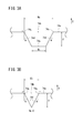
- 3A and 3B are views showing dimensions and angles of the groove section.
- FIG. 4 is a diagram showing a conductive film manufacturing apparatus according to the present embodiment.
- 5A to 5C are diagrams showing a manufacturing process of the sheet-like mold.
- FIG. 6 is a flowchart showing a manufacturing process of the conductive film according to the present embodiment.
- ⁇ indicating a numerical range is used as a meaning including numerical values described before and after the numerical value as a lower limit value and an upper limit value.
- FIG. 1 is an exploded perspective view of a touch panel module 10 using a conductive film 16.
- the touch panel module 10 has a sensor body 12 and a control circuit (not shown).
- the sensor body 12 includes a laminated conductive film 18 formed by laminating a first conductive film 16A and a second conductive film 16B, and a cover layer 20 made of, for example, glass laminated thereon.
- the laminated conductive film 18 and the cover layer 20 are arranged on a display panel 24 in a display device 22 such as a liquid crystal display.
- the first conductive film 16 ⁇ / b> A and the second conductive film 16 ⁇ / b> B include the first sensor region 26 ⁇ / b> A and the second sensor region 26 ⁇ / b> B corresponding to the display screen 24 a of the display panel 24 and the outer periphery of the display panel 24 when viewed from the top.
- a plurality of electrode patterns are formed by a transparent conductive layer composed of fine metal wires.
- Each electrode pattern has a net shape formed by combining a large number of cells, and extends in the first direction (y direction) shown in FIG.
- the plurality of electrode patterns are arranged in a second direction (x direction) orthogonal to the first direction.
- the “cell” refers to a shape that is two-dimensionally partitioned by a plurality of fine metal wires.
- the first conductive film 16A is electrically connected to the first terminal wiring portion 44a by a fine metal wire through the first connection portion 42a to one end portion of the first electrode pattern 36A.
- the first terminal wiring portion 44a led out from each first connection portion 42a is routed toward the substantially central portion of one long side of the first conductive film 16A, and is electrically connected to the corresponding first terminal portion 46a.
- An electrode film 48 is formed in the first terminal wiring region 28A, and the electrode film 48 and the first ground terminal portion 50a are electrically connected.
- a plurality of electrode patterns are formed by a transparent conductive layer composed of fine metal wires.
- Each electrode pattern has a net shape formed by combining a large number of cells, and extends in the second direction (x direction) shown in FIG.
- the plurality of electrode patterns are arranged in the first direction (y direction).
- the second conductive film 16B is electrically connected to one end of each second electrode pattern 36B by a second terminal wiring portion 44b made of a fine metal wire via a second connection portion 42b. It is connected.
- the second terminal wiring portion 44b led out from each second connection portion 42b is routed toward a substantially central portion on one long side of the second conductive film 16B, and is electrically connected to the corresponding second terminal portion 46b.
- a ground line for the purpose of shielding effect so as to surround the second sensor region 26B from one second ground terminal portion 50b to the other second ground terminal portion 50b. 52 is formed.
- the first alignment mark 62a and the second alignment mark 62b are preferably formed.
- the first alignment mark 62a and the second alignment mark 62b become a new composite alignment mark when the first conductive film 16A and the second conductive film 16B are bonded to form the laminated conductive film 18, and this composite alignment mark is formed.
- the alignment mark may be used as an alignment mark for positioning used when the laminated conductive film 18 is installed on the display panel 24.
- a dummy electrode may be formed in addition to the first electrode pattern 36A and the second electrode pattern 36B.
- the dummy electrode is electrically insulated from other electrodes so as not to affect the detection function and operation function of the first electrode pattern 36A and the second electrode pattern 36B.
- FIG. 2 is a cross-sectional view showing the conductive film 16 according to the present embodiment with a part thereof omitted.
- the conductive film 16 includes a thin metal wire 76 on the surface layer of the film member 70.
- the film member 70 includes a substrate 72 and a matrix layer 74 laminated on the substrate 72.
- the matrix layer 74 has a bank portion 74a and a net-like groove portion 74b on the surface.
- the fine metal wires 76 are filled in the groove portions 74 b and form a net-like electrode pattern along the surface layer of the matrix layer 74.
- the substrate 72 is a film-like member having predetermined transparency and flexibility.
- materials that can be used for the substrate 72 include polyethylene terephthalate (PET), polycarbonate (PC), polymethyl methacrylate (PMMA), polyimide (PI), acrylic (Acryl), polyethyllene naphthalate (PEN), and triacetate cellulose.
- Resins such as (TAC) and polyethersulfone (PES).
- the thickness of the substrate 72 is preferably 25 ⁇ m to 250 ⁇ m. Further, the light transmittance of the substrate 72 is preferably 80% or more, and more preferably 90% or more.
- the matrix layer 74 is laminated on one surface of the substrate 72.
- a resin having predetermined transparency and flexibility can be used for the matrix layer 74.
- a prepolymer, an oligomer, and / or a monomer having a polymerizable unsaturated bond or an epoxy group in the molecule, and an ultraviolet curable resin in which a photopolymerization initiator or an additive is mixed as necessary are suitable.
- the ultraviolet curable resin preferably has photosensitivity and cures in a short time in response to ultraviolet energy.
- Examples of the prepolymer and oligomer in the ultraviolet curable resin include unsaturated polyesters such as a condensation product of an unsaturated dicarboxylic acid and a polyhydric alcohol, methacrylates such as polyester methacrylate, polyether methacrylate, polyol methacrylate, melamine methacrylate, and polyester.
- unsaturated polyesters such as a condensation product of an unsaturated dicarboxylic acid and a polyhydric alcohol
- methacrylates such as polyester methacrylate, polyether methacrylate, polyol methacrylate, melamine methacrylate
- polyester examples include acrylates such as acrylates, epoxy acrylates, urethane acrylates, polyether acrylates, polyol acrylates, and melamine acrylates, and cationic polymerization type epoxy compounds.
- Examples of the monomer in the ultraviolet curable resin include styrene monomers such as styrene and ⁇ -methylstyrene, methyl acrylate, 2-ethylhexyl acrylate, methoxyethyl acrylate, butoxyethyl acrylate, butyl acrylate, and acrylic acid.
- styrene monomers such as styrene and ⁇ -methylstyrene, methyl acrylate, 2-ethylhexyl acrylate, methoxyethyl acrylate, butoxyethyl acrylate, butyl acrylate, and acrylic acid.
- Acrylic esters such as methoxybutyl and phenyl acrylate, methyl methacrylate, ethyl methacrylate, propyl methacrylate, methoxyethyl methacrylate, ethoxymethyl methacrylate, phenyl methacrylate, lauryl methacrylate and the like, acrylic Acid-2- (N, N-diethylamino) ethyl, acrylic acid-2- (N, N-dimethylamino) ethyl, acrylic acid-2- (N, N-dibenzylamino) methyl, acrylic acid-2- ( N, N-diethylami )
- Unsaturated substituted amino alcohol esters such as propyl, unsaturated carboxylic acid amides such as acrylamide and methacrylamide, ethylene glycol diacrylate, propylene glycol diacrylate, neopentyl glycol diacrylate, 1,6-hexanediol diacrylate , Compound
- Examples of the photopolymerization initiator include acetophenones, benzophenones, Michler benzoylbenzoate, methyl o-benzoylbenzoate, aldoxime, tetramethylmeurum monosulfide, thioxanthone, and / or n- photosensitizer.
- Examples include butylamine, triethylamine, and tri-butylphosphine.
- the ultraviolet curable resin is disclosed in the specification of International Publication No. 2007/034643.
- the matrix layer 74 has, on the surface, a bank portion 74a divided into a net-like electrode pattern and a groove portion 74b formed so as to coincide with the net-like electrode pattern.
- the groove portion 74b and the bank portion 74a are formed by pressing the mold against the surface of the matrix layer 74.
- the cross-sectional shape of the groove 74b will be described later.
- the fine metal wires 76 are filled in the grooves 74b to form a net-like electrode pattern.
- an ink for example, a material obtained by curing a conductive silver (Ag) paste such as REXALPHA (registered trademark) RF FS 015 manufactured by Toyo Ink Co., Ltd. can be used.
- conductive silver paste pasty copper (Cu), silver (Ag) -carbon (C), aluminum (Al), nickel (Ni), chromium (Cr), nickel (Ni) -phosphorus (P) Carbon black (C) can be used.
- the width and depth of the thin metal wire 76 are preferably the same as those of the groove 74b.
- the inventors of the present invention have found that by devising the cross-sectional shape of the groove 74b formed on the surface of the matrix layer 74, it is possible to fill the groove 74b with insufficient viscosity.
- the cross-sectional shape of the groove 74b will be described.
- FIG. 3A and 3B are diagrams showing dimensions and angles of the cross section of the groove 74b.
- the cross-sectional shape of the groove 74b is a trapezoid or a triangle.
- FIG. 3A shows a trapezoidal cross section and
- FIG. 3B shows a triangular cross section.
- the trapezoidal groove 74b has an opening 74c, two inner wall side surfaces 74d facing each other, and a bottom 74e, and faces each other from the opening 74c toward the bottom 74e.
- the interval between the inner wall side surfaces 74d is narrow. As shown in FIG.
- the groove 74b having a triangular cross section includes an opening 74c and two inner wall side surfaces 74d facing each other, and the inner wall side surfaces 74d facing each other from the opening 74c toward the bottom.
- the interval is narrowed and the inner wall side surfaces 74d are connected to each other at the bottom.
- the cross-sectional shape of the groove 74b can be indicated by the following conditions.
- the width of the opening 74c and W O, the width of the bottom 74e and W B, the depth is d, the inner wall side surface of the groove portion 74b with respect to the direction (V direction in FIG. 3A and 3B) perpendicular to the surface of the film member 70
- the groove 74b is W O > W B 0 ⁇ ⁇ 53.74 ⁇ (d / W O ) +50 0 ⁇ ⁇ 64 0.2 ⁇ W O ⁇ 4
- the relationship 0.1 ⁇ d ⁇ 5 is satisfied.
- Units of ⁇ is deg, d, W O, and W both units of B is [mu] m.
- the inclination angle of the inner wall side surface 74d with respect to the bank portion 74a of the matrix layer 74 is gentle. For this reason, when ink is removed from the bank portion 74a of the matrix layer 74 after the groove portion 74b is filled with ink, the ink filled in the groove portion 74b may be peeled off, and ink filling in the groove portion 74b may be insufficient. . Further, the condition for W O ⁇ 0.2 is that the opening 74c of the groove 74b is narrow. For this reason, when filling the groove 74b with ink, it is difficult for ink to enter the groove 74b, and there is a possibility that ink filling the groove 74b is insufficient.
- the condition that W O > 4 is that the opening 74c of the groove 74b is wide. For this reason, ⁇ > 6 Similar to the condition of 4, there is a possibility that the ink filling into the groove 74b is insufficient.
- the condition for d ⁇ 0.1 is that the depth d of the groove 74b is shallow. For this reason, ⁇ > 64 and W O > Similar to the condition of 4, there is a possibility that the ink filling into the groove 74b is insufficient.
- the condition for d> 5 is that the depth d of the groove 74b is deep. For this reason, when filling the groove 74b with ink, it is difficult to fill the ink up to the bottom of the groove 74b. In this case, some ink may fall to the bottom after filling. For this reason, when ⁇ , W 2 O, and d are not within the appropriate ranges, there is a high possibility that the fine metal wires 76 are disconnected.
- FIG. 4 is a diagram showing a conductive film manufacturing apparatus 100 according to the present embodiment.
- a roll-to-roll apparatus is shown here.
- a film-like processed product conveyed between processing stations for example, a film-like substrate or a film member in which a matrix layer is laminated on a substrate is simply referred to as a film.
- the conductive film manufacturing apparatus 100 includes a substrate feeding unit 110, a matrix layer stacking unit 120, a matrix layer surface forming unit 130, an ink filling unit 140, an ink removing unit 150, in order from the upstream side to the downstream side in the film conveyance direction. Processing stations such as an ink curing unit 160, a cleaning unit 170, and a substrate winding unit 180 are arranged.
- the substrate feeding unit 110 includes a film-like substrate 72 wound in a roll shape, and sends the substrate 72 downstream at a predetermined feeding speed.
- the matrix layer stacking unit 120 is disposed on the downstream side of the substrate feeding unit 110 in the film conveyance direction.
- the matrix layer stacking unit 120 includes an application unit 122 that stacks a liquid matrix layer 74 ′ by applying a liquid ultraviolet curable resin to the surface of the substrate 72.
- an application unit 122 for example, a roll coater or an extrusion film forming apparatus is used.
- the matrix layer surface forming unit 130 is disposed downstream of the matrix layer stacking unit 120 in the film conveyance direction.
- the matrix layer surface forming unit 130 includes a pressing unit 132 and an ultraviolet irradiation unit 138.
- the pressing part 132 has a cylindrical mold 134 disposed on the surface side of the film, that is, on the matrix layer 74 side.
- the mold 134 includes a cylindrical roller 135 and a metal sheet-shaped mold 136 that is wound around and fixed to the outer peripheral surface of the roller 135.
- a convex portion 136 b that matches the groove pattern transferred to the matrix layer 74 is formed.
- FIG. 5A to FIG. 5C are diagrams showing a manufacturing process of the sheet-like mold 136.
- a net-like electrode pattern and a groove 137b having the same pattern are formed on one surface of a glass plate 137 to make a prototype of a sheet-like mold 136.
- a method for forming the groove 137b in the glass plate 137 for example, the technique disclosed in the specification of International Publication No. 2004/112119 can be used.
- a technique of forming a groove having a tapered cross section on the surface of a silicon substrate using an inductively coupled plasma (ICP) is shown.
- ICP inductively coupled plasma
- a gas mixture for etching for example, SF 6 gas
- a fluorocarbon gas for deposition for example, C 4 F 8 gas
- oxygen gas is used as a process gas, and by controlling the flow rate of each gas, The taper shape of the groove formed on the silicon substrate surface is controlled.
- ⁇ can be increased as the oxygen flow rate is increased, and ⁇ can be decreased as the oxygen flow rate is decreased.
- the technique disclosed in Japanese Patent Application Laid-Open No. 2007-158107 can be used as a method of forming the groove 137b in the glass plate 137.
- a technique for adjusting the cross-sectional shape of the groove formed on the surface of the silicon substrate by controlling the etching parameters (RF power, gas pressure, gas type, gas flow rate, etc.) of dry etching is shown.
- RF power RF power
- gas pressure gas pressure
- gas type gas flow rate
- etching parameters RF power, gas pressure, gas type, gas flow rate, etc.
- a groove 137b having the same pattern as the net-like electrode pattern and having a trapezoidal or triangular shape is formed on one surface of the glass plate 137.
- Ni nickel
- FIG. 5C when the Ni sheet 136 ′ having a necessary thickness is formed on the surface of the glass plate 137 on the groove 137 b side, the glass plate 137 is removed from the Ni sheet 136 ′ to form a sheet-like mold 136. .
- the Ni sheet-shaped mold 136 is wound around the outer peripheral surface of the roller 135 and fixed, the mold 134 is completed.
- the matrix layer 74 of the conductive film 16 and the mold 134 can be easily separated when the conductive film 16 is manufactured.
- the surface treatment for example, SiO 2 having a thickness of about 1200 to 1500 mm can be formed by sputtering, and various other types of surface treatment can be performed.
- the ultraviolet irradiation unit 138 is disposed on the back side of the film, that is, on the substrate 72 side, and is disposed at the same position as the pressing unit 132 or slightly downstream in the film transport direction.
- the ultraviolet irradiation unit 138 irradiates the film with ultraviolet light 139 of about 100 to 400 nm.
- the ultraviolet light 139 causes a chemical reaction (photopolymerization reaction) with the matrix layer 74 'to cure them.
- a light source of the ultraviolet irradiation unit 138 an ultrahigh pressure mercury lamp, a high pressure mercury lamp, a low pressure mercury lamp, a carbon arc, a xenon arc, a metal halide lamp, or the like can be used. These light sources may be either air-cooled or water-cooled, but are more preferably water-cooled.
- An ink filling unit 140 is disposed downstream of the matrix layer surface forming unit 130 in the film conveyance direction.
- the ink filling unit 140 includes an ink supply unit 142 and a squeegee unit 144.
- the ink supply unit 142 applies paste-like ink 76 ′ containing metal particles that are the material of the fine metal wires 76 to the surface of the matrix layer 74.
- the ink 76 ' may be supplied continuously or discontinuously, for example, at a predetermined interval.
- the supply amount of the ink 76 ' is determined according to the film conveyance speed.
- the squeegee unit 144 is disposed downstream of the ink supply unit 142 in the film transport direction.
- the squeegee unit 144 includes a first squeegee blade 146 that applies the ink 76 ′ supplied to the surface of the matrix layer 74 to the surface of the matrix layer 74, a first squeegee holder 148 that holds the first squeegee blade 146,
- the first squeegee blade 146 is formed of urethane rubber, silicon rubber, metal or the like, and the width thereof is the same as or larger than the width of the film.
- the first squeegee blade 146 has an angle between the blade and the surface of the matrix layer 74 such that the blade width direction is orthogonal to the film conveying direction, the blade tip is in contact with the surface of the matrix layer 74, and It arrange
- the first squeegee blade 146 pushes and fills a portion of the ink 76 ′ into the groove 74 b of the matrix layer 74 while rubbing the surface of the matrix layer 74 in the direction opposite to the film transport direction, and at the same time, the matrix layer 74.
- the ink 76 ' is removed from the surface of the bank portion 74a.
- a drive device may be provided in the squeegee unit 144 so that the first squeegee blade 146 is driven.
- the driving direction of the first squeegee blade 146 can be freely set.
- An ink removing unit 150 is disposed downstream of the ink filling unit 140 in the film conveyance direction.
- the ink removing unit 150 includes a second squeegee blade 152 that removes ink 76 ′ remaining on the surface of the bank portion 74 a of the matrix layer 74, and a second squeegee holder 154 that holds the second squeegee blade 152.
- the second squeegee blade 152 is made of urethane rubber, silicon rubber, metal or the like, and the width thereof is the same as or larger than the width of the film.
- the second squeegee blade 152 has an angle between the blade and the surface of the matrix layer 74 such that the blade width direction is orthogonal to the film transport direction, the blade tip is in contact with the surface of the matrix layer 74, and It arrange
- An ink curing unit 160 is disposed downstream of the ink removing unit 150 in the film conveyance direction.
- the ink curing unit 160 includes a heater 162.
- the heater 162 radiates heat, hot air, infrared rays, and near infrared rays necessary to cure the ink 76 ′ filled in the grooves 74 b of the matrix layer 74 toward the matrix layer 74.
- a cleaning unit 170 is disposed downstream of the ink curing unit 160 in the film conveyance direction.
- the cleaning unit 170 includes a support roll 172 and a cleaning roll 174.
- the support roll 172 supports the film from the substrate 72 side.
- the cleaning roll 174 contacts the surface of the matrix layer 74 and cleans the bank portion 74a.
- the cleaning roll 174 may contain a cleaning liquid.
- As the cleaning liquid for example, a mixed liquid in which isopropyl alcohol and acetone are mixed at 9: 1 to 8: 2 can be used.
- the cleaning unit 170 may include a plurality of support rolls 172.
- a substrate winding unit 180 is disposed downstream of the cleaning unit 170 in the film conveyance direction.
- the substrate winding unit 180 winds the cleaned film, that is, the conductive film 16 on a roll.
- the ink filling unit 140, the ink removing unit 150, and the ink curing unit 160 may be a single unit, and a plurality of units may be arranged between the matrix layer surface forming unit 130 and the cleaning unit 170.
- the ink filling step, the ink removing step, and the ink curing step are performed a plurality of times, and the metal thin wires 76 filled in the groove portions 74b of the matrix layer 74 become a plurality of layers.
- the type of the metal material is changed between the units, the fine metal wires 76 filled in the grooves 74b of the matrix layer 74 become different metal layers.
- the conductive film manufacturing apparatus 100 of FIG. 4 is a roll-to-roll system, a single wafer type apparatus can also be used.
- FIG. 6 is a flowchart showing a manufacturing process of the conductive film according to the present embodiment. The manufacturing method of the electroconductive film which concerns on this Embodiment shown in FIG. 6 is demonstrated with reference to a figure suitably.
- the film is conveyed from the substrate feeding unit 110 to the matrix layer stacking unit 120.
- a matrix layer stacking process for stacking the matrix layer 74 ′ on the substrate 72 is performed (step S71). Specifically, an ultraviolet curable resin is applied to the substrate 72 and the matrix layer 74 ′ is laminated. At this stage, the matrix layer 74 'is not cured.
- step S71 the film is conveyed from the matrix layer laminating unit 120 to the matrix layer surface forming unit 130.
- a matrix layer surface forming process for forming a bank part 74a and a net-like groove part 74b on the surface of the matrix layer 74 ′ is performed (step S72).
- a pattern formed on the surface of the mold 134 is formed by pressing the mold 134 onto the surface of the matrix layer 74 ′ with a predetermined pressure while synchronizing the rotational speed of the mold 134 with the film conveyance speed. Transfer to the surface of the layer 74 '.
- the ultraviolet light 139 is irradiated from the ultraviolet irradiation unit 138 to the film back side, that is, the substrate 72 side.
- the matrix layer 74 ′ undergoes a chemical reaction and becomes a cured matrix layer 74.
- step S72 the film is conveyed from the matrix layer surface forming unit 130 to the ink filling unit 140.
- the ink application member that is, the first squeegee blade 146 is slid along the surface of the matrix layer 74 to enter the groove 74 b.
- An ink filling process for filling the ink 76 ' is performed (step S73). Specifically, a predetermined amount of ink 76 ′ is supplied from the ink supply unit 142 to the surface of the matrix layer 74.
- the first squeegee blade 146 is disposed downstream of the ink supply position in the film transport direction so that the width direction of the front end is orthogonal to the film transport direction, and the front end is the surface of the matrix layer 74, strictly speaking,
- the surface of the bank 74a is brought into contact with a predetermined pressure.
- the first squeegee blade 146 moves relative to the matrix layer 74 in the direction opposite to the film transport direction.
- the ink 76 ' is removed by rubbing the bank portion 74a, and the groove 76b is filled with the ink 76'.
- the film is conveyed from the ink filling unit 140 to the ink removing unit 150.
- the ink removing unit 150 performs an ink removing process of removing the ink 76 ′ remaining on the bank 74 a by sliding the ink removing member, that is, the second squeegee blade 152 along the surface of the matrix layer 74 (step S ⁇ b> 74).
- the second squeegee blade 152 is arranged so that the width direction of the tip thereof is orthogonal to the film transport direction, and the tip is predetermined on the surface of the matrix layer 74, strictly, the surface of the bank portion 74a. Contact with pressure.
- the second squeegee blade 152 moves relative to the matrix layer 74 in the direction opposite to the film conveying direction. By sliding the second squeegee blade 152 on the surface of the matrix layer 74 in this way, the remaining ink 76 'is removed by rubbing the bank portion 74a.
- step S74 the film is conveyed from the ink removing unit 150 to the ink curing unit 160.
- an ink curing process is performed in which the ink 76 'filled in the groove 74b is cured by heat treatment (step S75). For example, heat treatment is performed at 150 ° C. for about 3 to 10 minutes to cure the ink 76 ′ to form the fine metal wires 76.
- step S75 When the ink curing process (step S75) is completed, the film is conveyed from the ink curing unit 160 to the cleaning unit 170. In the cleaning unit 170, a cleaning process for cleaning the surface of the matrix layer 74 with the cleaning roll 174 is performed (step S76).
- step S76 When the cleaning process (step S76) is completed, the conductive film 16 is completed.
- the conductive film 16 is taken up by the substrate take-up unit 180, and the series of processes ends.
- the cross-sectional shape of the groove 74b formed on the surface of the film member 70 is a shape that easily causes capillary action. For this reason, the ink 76 'can be sufficiently filled when the ink 76' is filled in the groove 74b. In addition, the ink 76 ′ filled with the cross-sectional shape of the groove 74b is easy to fasten. For this reason, when the ink 76 ′ remaining on the surface of the film member 70 is removed, the removal of the ink 76 ′ from the groove 74 b can be suppressed. Therefore, disconnection of the fine metal wire 76 is difficult to occur.
- the present inventors produced a plurality of evaluation conductive films in which an electrode pattern for evaluation was formed, and examined whether or not a disconnection occurred in the thin metal wire of each conductive film. .
- the cross-sectional shape of the groove on the surface of the film member was varied between the conductive films. Specifically, the angle formed by the width W O [ ⁇ m] of the opening, the width W B [ ⁇ m] of the bottom, the depth d [ ⁇ m], and the inner wall side surface of the groove with respect to the direction perpendicular to the surface of the film member. ⁇ was varied between the conductive films.
- Examples 15 to 15 are conductive films of 15 patterns satisfying ⁇ ⁇ 64, the fourth condition 0.2 ⁇ W O ⁇ 4, and the fifth condition 0.1 ⁇ d ⁇ 5.
- a continuity test was conducted using Comparative Examples 1 to 8 as eight patterns of conductive films that did not satisfy at least one of the first to fifth conditions.
- Tables 1 to 5 below show the dimensions and angles of the groove portions in Examples 1 to 15 and Comparative Examples 1 to 8 and the presence or absence of disconnection.
- the calculated parameter values in the following Tables 1 to 5 are calculated values of 53.74 ⁇ (d / W O ) +50 in the second condition.
- the conductive film and the touch panel module according to the present invention are not limited to the above-described embodiments, and various configurations can be adopted without departing from the gist of the present invention.
Landscapes
- Engineering & Computer Science (AREA)
- General Engineering & Computer Science (AREA)
- Theoretical Computer Science (AREA)
- Human Computer Interaction (AREA)
- Physics & Mathematics (AREA)
- General Physics & Mathematics (AREA)
- Position Input By Displaying (AREA)
- Manufacturing Of Printed Wiring (AREA)
Abstract
ナノインプリントによってフィルム表面に網状の金属細線を形成する際に、フィルム表面の溝部に対するインクの充填不良を起こりにくくすることによって、金属細線の断線が起こりにくい導電性フィルム及びこの導電性フィルムを用いたタッチパネルモジュールを提供する。フィルム部材の表面に形成される溝部の断面形状のうち、開口部の幅をWOとし、底部の幅をWBとし、深さをdとし、フィルム部材の表面と直交する方向に対する溝部の内壁側面の成す角度をθとした場合に、溝部が、 WO>WB 0<θ≦53.74×(d/WO)+50 0<θ≦64 0.2≦WO≦4 0.1≦d≦5という関係を満たす。
Description
本発明は、導電性フィルム及びタッチパネルモジュールに関し、例えば投影型静電容量方式のタッチパネルに用いて好適な導電性フィルム及びこの導電性フィルムを用いたタッチパネルモジュールに関する。
近年、スマートフォンやタブレット型PC(パーソナルコンピュータ)のように、携帯型電子機器の入力装置としてタッチパネルの使用が増えている。これらの機器では、操作性、携帯性、意匠性の高さ等が求められる。例えば、機器の一部又は全体を曲面形状とすることによって、身体の一部に装着して使用でき、また、入力装置を表示画面だけでなく機器の側面部分や稜線部分にも付与することによって、小型の機器であっても操作性を向上させることが可能となる。また、機器の外装カバーにタッチセンサ機能を付与すれば、部品点数を削減でき、機器の小型化とそれによる携帯性の向上が実現可能となる。さらに、タッチパネルを立体形状等の自由な形状に作ることができるのであれば、機器を自由にデザインすることができ、意匠性の高い装置を作製することが可能となる。
従来のタッチパネルには、ガラス基板上若しくはフィルム基板上に形成したITO(インジウム・ティン・オキサイド)薄膜にパターニングを施したセンサ部材が使用されていた。しかし、ガラス基板は堅く曲面形状を形成することが難しい。また、フィルム基板上に形成したITO薄膜は屈曲性に乏しく、フィルム基板の屈曲に応じて容易にクラックが発生して断線故障を発生する。このため、タッチパネルの形状には制約があった。また、希少金属であるインジウムを使用するため、資源の枯渇懸念による製品の供給安定性にも懸念があった。
特許文献1は、ITO薄膜を使用しない導電性フィルム、具体的には、可撓性を有するフィルム基板上に網状の金属細線が形成された導電性フィルムを示している。網状の金属細線が形成された導電性フィルムは、タッチパネルとして実用上問題のない透明性を確保しつつ、導電性を維持できる。また、金属細線は導電性フィルムが折り曲げられても断線しない。この導電性フィルムを携帯型電子機器のタッチパネルに使用すれば、機器を自由にデザインすることができる。
網状の金属細線をフィルム基板にパターニングする手法としては、導電性インク(以下、単に「インク」という)を用いてスクリーン印刷する方法や、インクジェット方式によって描画する方法や、ナノインプリントによってフィルム表面に溝をパターニングした後に導電ペーストを埋め込む方法等が知られている。これらの中でも、ナノインプリントを使用する方法は、金属細線のエッジ部分を滑らかに形成することができるため、好ましい。
ナノインプリントによってフィルム表面に金属細線を形成する方法は次のような工程からなる。
(1)所望の電極パターンを付与した転写用の金型を作製する。
(2)フィルム表面に紫外線硬化性の樹脂を塗布する。
(3)硬化前の樹脂に金型を押し付けた状態で紫外線を照射し、樹脂を硬化させる。
(4)金型を外した後に樹脂表面に転写された溝にインクを充填する。
(1)所望の電極パターンを付与した転写用の金型を作製する。
(2)フィルム表面に紫外線硬化性の樹脂を塗布する。
(3)硬化前の樹脂に金型を押し付けた状態で紫外線を照射し、樹脂を硬化させる。
(4)金型を外した後に樹脂表面に転写された溝にインクを充填する。
ナノインプリントによってフィルム表面に金属細線を形成する方法において、溝にインクを充填する際にインクの充填が不十分であると、インクが充填されていない部分が導通不良箇所となる。導電性フィルムをセンサーフィルムとして機能させる場合、導通不良箇所があると検出エラーが発生する。このため、ナノインプリントによってフィルム表面に網状の金属細線が形成された導電性フィルム部材において、インクの充填不良による断線の抑制が課題となっていた。
本発明者らは、ナノインプリントによってフィルム表面に金属細線を形成する上記(1)~(4)のプロセスを検討した。その結果、インクが充填される溝の内壁側面が、フィルム表面に対して垂直であることによって、インクの充填が阻害されることを見出した。その原因はインクの粘性にあると考えられる。溝に対するインクの充填は毛細管現象を利用している。しかし、粘性が高いインクは、毛細管現象のように細管部に液体が充填されるような物理現象に対しては不利である。毛細管現象によるインクの充填が十分発現されるようにインクの粘性を下げたとする。この場合、インク内に含まれる導電性金属成分の固形分量が低下し、インクの溶剤成分が揮発したあとに金属細線に残る金属量が低減する。その結果、金属細線の抵抗値が上昇し、タッチパネルの動作に支障をきたす虞がある。
本発明はこのような課題を考慮してなされたものであり、ナノインプリントによってフィルム表面に網状の金属細線を形成する際に、フィルム表面の溝部に対するインクの充填不良を起こりにくくすることによって、金属細線の断線が起こりにくい導電性フィルム及びこの導電性フィルムを用いたタッチパネルモジュールを提供することを目的とする。
本発明に係る導電性フィルムは、可撓性を有するフィルム部材の表面に金属細線からなる網状の導電パターンを具える導電性フィルムにおいて、金属細線が、フィルム部材の表面に形成された溝部に充填された金属材料からなり、溝部の断面形状のうち、開口部の幅をWOとし、底部の幅をWBとし、深さをdとし、フィルム部材の表面と直交する方向に対する溝部の内壁側面の成す角度をθとすると、溝部が、
WO>WB
0<θ≦53.74×(d/WO)+50
0<θ≦64
0.2≦WO≦4
0.1≦d≦5という関係を満たしていることを特徴とする。但し、θの単位はdegであり、d、WO、及びWBの単位はいずれもμmである。
WO>WB
0<θ≦53.74×(d/WO)+50
0<θ≦64
0.2≦WO≦4
0.1≦d≦5という関係を満たしていることを特徴とする。但し、θの単位はdegであり、d、WO、及びWBの単位はいずれもμmである。
また、本発明において、溝部がフィルム部材に設けられたマトリックス層に形成されてもよい。
また、本発明において、マトリックス層が光硬化性樹脂であってもよい。
また、本発明において、金属材料がAgからなるようにしてもよい。
また、本発明に係るタッチパネルモジュールは、本発明の導電性フィルムを用いることを特徴とする。
本発明に係る導電性フィルムによれば、フィルム部材の表面に形成される溝部の断面形状が毛細管現象を起しやすい形状になっている。このため、溝部へのインクの充填時にインクを十分に充填できる。また、溝部の断面形状が充填されたインクを留めやすい形状になっている。このため、フィルム部材の表面に残留するインクを除去する際に、溝部からインクが除去されることを抑制できる。したがって、金属細線の断線が起こりにくくなる。
またこのような導電性フィルムを用いたタッチパネルモジュールは、断線に起因する動作不良が起こりにくくなる。
以下、本発明に係る導電性フィルムをタッチパネルモジュールに適用した実施の形態例を図1~図6を参照しながら説明する。なお、本明細書において数値範囲を示す「~」は、その前後に記載される数値を下限値及び上限値として含む意味として使用される。
[本実施の形態]
<タッチパネルモジュールの構成>
図1は導電性フィルム16を使用するタッチパネルモジュール10の分解斜視図である。
<タッチパネルモジュールの構成>
図1は導電性フィルム16を使用するタッチパネルモジュール10の分解斜視図である。
図1に示すように、タッチパネルモジュール10は、センサ本体12と制御回路(図示せず)とを有する。センサ本体12は、第1導電性フィルム16Aと第2導電性フィルム16Bとを積層して構成された積層導電性フィルム18と、その上に積層された例えばガラス製のカバー層20とを有する。積層導電性フィルム18及びカバー層20は、例えば液晶ディスプレイ等の表示装置22における表示パネル24上に配置されるようになっている。第1導電性フィルム16A及び第2導電性フィルム16Bは、上面から見たときに、表示パネル24の表示画面24aに対応した第1センサ領域26A及び第2センサ領域26Bと、表示パネル24の外周部分に対応する第1端子配線領域28A及び第2端子配線領域28B(いわゆる額縁)と、第1センサ領域26Aから第1端子配線領域28Aにかけて形成された第1導電部30Aと、第2センサ領域26Bから第2端子配線領域28Bにかけて形成された第2導電部30Bとを有する。
第1センサ領域26Aには、金属細線にて構成された透明導電層による複数の電極パターンが形成されている。各電極パターンは、多数のセルが組み合わされて構成された網状であり、図1で示す第1方向(y方向)に延在する。また、複数の電極パターンは、第1方向と直交する第2方向(x方向)に配列されている。ここで、「セル」とは、複数の金属細線によって二次元的に区画された形状を指す。
図1に示すように、第1導電性フィルム16Aは、第1電極パターン36Aの各一方の端部にそれぞれ第1結線部42aを介して金属細線による第1端子配線部44aが電気的に接続されている。各第1結線部42aから導出された第1端子配線部44aは、第1導電性フィルム16Aの一方の長辺における略中央部に向かって引き回され、それぞれ対応する第1端子部46aに電気的に接続されている。また、第1端子配線領域28Aには、電極膜48が形成され、この電極膜48と第1接地端子部50aとが電気的に接続されている。
第2センサ領域26Bには、金属細線にて構成された透明導電層による複数の電極パターンが形成されている。各電極パターンは、多数のセルが組み合わされて構成された網状であり、図1で示す第2方向(x方向)に延在する。また複数の電極パターンは、第1方向(y方向)に配列されている。
図1に示すように、第2導電性フィルム16Bは、各第2電極パターン36Bの一方の端部に、それぞれ第2結線部42bを介して金属細線による第2端子配線部44bが電気的に接続されている。各第2結線部42bから導出された第2端子配線部44bは、第2導電性フィルム16Bの一方の長辺における略中央部に向かって引き回され、それぞれ対応する第2端子部46bに電気的に接続されている。また、第2端子配線部44bの外側には、一方の第2接地端子部50bから他方の第2接地端子部50bにかけて、第2センサ領域26Bを囲むように、シールド効果を目的とした接地ライン52が形成されている。
図1に示すように、第1導電性フィルム16Aと第2導電性フィルム16Bの例えば各コーナー部に、第1導電性フィルム16Aと第2導電性フィルム16Bの貼り合わせの際に使用する位置決め用の第1アライメントマーク62a及び第2アライメントマーク62bを形成することが好ましい。この第1アライメントマーク62a及び第2アライメントマーク62bは、第1導電性フィルム16Aと第2導電性フィルム16Bを貼り合わせて積層導電性フィルム18とした場合に、新たな複合アライメントマークとなり、この複合アライメントマークは、該積層導電性フィルム18を表示パネル24に設置する際に使用する位置決め用のアライメントマークとして利用してもよい。
なお、第1電極パターン36Aと第2電極パターン36Bの他にダミー電極が形成されていてもよい。ダミー電極は、第1電極パターン36Aと第2電極パターン36Bの検出機能と動作機能に影響を与えないように他の電極と電気的に絶縁される。
以下において、導電性フィルムの構成や製造装置及び製造方法について実施の形態を説明する。
<導電性フィルム>
図2は本実施の形態に係る導電性フィルム16を一部省略して示す断面図である。導電性フィルム16は、フィルム部材70の表層に金属細線76を具える。フィルム部材70は、基板72と基板72に積層されるマトリックス層74からなる。マトリックス層74は、表面に土手部74aと網状の溝部74bを有する。金属細線76は、溝部74bに充填されており、マトリックス層74の表層に沿って網状の電極パターンを形成する。
図2は本実施の形態に係る導電性フィルム16を一部省略して示す断面図である。導電性フィルム16は、フィルム部材70の表層に金属細線76を具える。フィルム部材70は、基板72と基板72に積層されるマトリックス層74からなる。マトリックス層74は、表面に土手部74aと網状の溝部74bを有する。金属細線76は、溝部74bに充填されており、マトリックス層74の表層に沿って網状の電極パターンを形成する。
基板72は所定の透明度と可撓性を有するフィルム状の部材である。基板72に使用できる材料としては、例えば、ポリエチレンテレフタレート(PET)、ポリカーボネート(PC)、ポリメチルメタクリレート(PMMA)、ポリイミド(PI)、アクリル(Acryl)、ポルリエチルレンナフタレート(PEN)、トリアセテートセルロース(TAC)、ポリエーテルスルホン(PES)等の樹脂が挙げられる。基板72の厚さは25μm~250μmが好ましい。また、基板72の光線透過率は80%以上が好ましく、90%以上がより好ましい。
マトリックス層74は基板72の一面に積層される。マトリックス層74には所定の透明度と可撓性を有する樹脂を使用できる。特に、分子中に重合性不飽和結合又はエポキシ基を有するプレポリマー、オリゴマー、及び/又はモノマー、また必要に応じて光重合開始剤や添加剤を混合した紫外線硬化樹脂が好適である。紫外線硬化樹脂は感光性を持ち、紫外線のエネルギーに反応して短時間で硬化するものが好ましい。
紫外線硬化樹脂中のプレポリマー、オリゴマーとしては、例えば、不飽和ジカルボン酸と多価アルコールの縮合物等の不飽和ポリエステル類、ポリエステルメタクリレート、ポリエーテルメタクリレート、ポリオールメタクリレート、メラミンメタクリレート等のメタクリレート類、ポリエステルアクリレート、エポキシアクリレート、ウレタンアクリレート、ポリエーテルアクリレート、ポリオールアクリレート、メラミンアクリレート等のアクリレート、カチオン重合型エポキシ化合物が挙げられる。
紫外線硬化樹脂中のモノマーとしては、例えば、スチレン、α-メチルスチレン等のスチレン系モノマー、アクリル酸メチル、アクリル酸-2-エチルヘキシル、アクリル酸メトキシエチル、アクリル酸ブトキシエチル、アクリル酸ブチル、アクリル酸メトキシブチル、アクリル酸フェニル等のアクリル酸エステル類、メタクリル酸メチル、メタクリル酸エチル、メタクリル酸プロピル、メタクリル酸メトキシエチル、メタクリル酸エトキシメチル、メタクリル酸フェニル、メタクリル酸ラウリル等のメタクリル酸エステル類、アクリル酸-2-(N,N-ジエチルアミノ)エチル、アクリル酸-2-(N,N-ジメチルアミノ)エチル、アクリル酸-2-(N,N-ジベンジルアミノ)メチル、アクリル酸-2-(N,N-ジエチルアミノ)プロピル等の不飽和置換の置換アミノアルコールエステル類、アクリルアミド、メタクリルアミド等の不飽和カルボン酸アミド、エチレングリコールジアクリレート、プロピレングリコールジアクリレート、ネオペンチルグリコールジアクリレート、1,6-ヘキサンジオールジアクリレート、トリエチレングリコールジアクリレート等の化合物、ジプロピレングリコールジアクリレート、エチレングリコールジアクリレート、プロピレングリコールジメタクリレート、ジエチレングリコールジメタクリレート等の多官能性化合物、及び/又は分子中に2個以上のチオール基を有するポリチオール化合物、例えば、トリメチローラプロパントリチオグリコレート、トリメチローラプロパントリチオプロピレート、ペンタエリスリトールテトラチオグリコレート等が挙げられる。
光重合開始剤としては、例えば、アセトフェノン類、ベンゾフェノン類、ミヒラーベンゾイルベンゾエート、o-ベンゾイル安息香酸メチル、アルドオキシム、テトラメチルメウラムモノサルファイド、チオキサントン、及び/又は光増感剤であるn-ブチルアミン、トリエチルアミン、トリ-ブチルホスフィン等が挙げられる。
なお、紫外線硬化樹脂に関しては国際公開第2007/034643号の明細書に開示されている。
マトリックス層74は、表面に、網状の電極パターンに区切られる土手部74aと、網状の電極パターンと一致するように形成される溝部74bと、を有する。溝部74bと土手部74aはマトリックス層74の表面への金型の押圧によって形成される。溝部74bの断面形状については後述する。
金属細線76は、溝部74bに充填されて網状の電極パターンを形成する。本実施の形態の金属細線76の材料としては、インク、例えば東洋インキ社製造のREXALPHA(登録商標)RF FS 015のような導電性銀(Ag)ペーストが硬化したものを使用できる。導電性銀ペーストの他にはペースト状の銅(Cu)、銀(Ag)-カーボン(C)、アルミニウム(Al)、ニッケル(Ni)、クロム(Cr)、ニッケル(Ni)-リン(P)、カーボンブラック(C)等が使用可能である。金属細線76の幅及び深さは溝部74bと同じであることが好ましい。
本発明者らは、マトリックス層74の表面に形成される溝部74bの断面形状を工夫することによって、粘性の高いインクを溝部74bに不足なく充填することが可能になることを発見した。以下において、溝部74bの断面形状について説明をする。
図3A及び図3Bは溝部74b断面の寸法と角度を示す図である。溝部74bの断面形状は、台形又は三角形である。図3Aは台形の断面を示し、図3Bは三角形の断面を示す。図3Aで示すように、断面が台形の溝部74bは、開口部74cと、互いに対向する2つの内壁側面74dと、底部74eと、からなり、開口部74cから底部74eに向かって、互いに対向する内壁側面74d同士の間隔が狭くなっている。図3Bで示すように、断面が三角形の溝部74bは、開口部74cと、互いに対向する2つの内壁側面74dと、からなり、開口部74cから底に向かって、互いに対向する内壁側面74d同士の間隔が狭くなり、底で内壁側面74d同士が繋がっている。
具体的に、溝部74bの断面形状は次の条件によって示すことができる。開口部74cの幅をWOとし、底部74eの幅をWBとし、深さをdとし、フィルム部材70の表面と直交する方向(図3A及び図3BのV方向)に対する溝部74bの内壁側面74dの成す角度をθとすると、溝部74bは、
WO>WB
0<θ≦53.74×(d/WO)+50
0<θ≦64
0.2≦WO≦4
0.1≦d≦5という関係を満たす。θの単位はdegであり、d、WO、及びWBの単位はいずれもμmである。
WO>WB
0<θ≦53.74×(d/WO)+50
0<θ≦64
0.2≦WO≦4
0.1≦d≦5という関係を満たす。θの単位はdegであり、d、WO、及びWBの単位はいずれもμmである。
θ>64となる条件は、マトリックス層74の土手部74aに対する内壁側面74dの傾斜角度が緩い。このため、溝部74bにインクを充填した後にマトリックス層74の土手部74aからインクを除去する際に溝部74b内部に充填したインクが剥ぎ取られ、溝部74bに対するインクの充填が不足する可能性がある。また、WO<0.2となる条件は、溝部74bの開口部74cが狭い。このため、溝部74bにインクを充填する際に溝部74bにインクが入りにくく、溝部74bに対するインクの充填が不足する可能性がある。また、WO>4となる条件は、溝部74bの開口部74cが広い。このため、θ>6
4となる条件と同様に、溝部74bに対するインクの充填が不足する可能性がある。また、d<0.1となる条件は、溝部74bの深さdが浅い。このため、θ>64及びWO>
4となる条件と同様に、溝部74bに対するインクの充填が不足する可能性がある。また、d>5となる条件は、溝部74bの深さdが深い。このため、溝部74bにインクを充填する際に溝部74bの底までインクが充填されにくい。この場合は一部のインクが充填後に底に落ち込む可能性がある。こうしたことからθ、WO及びdが適切な範囲内にない場合には金属細線76の断線が発生する可能性が高くなる。
4となる条件と同様に、溝部74bに対するインクの充填が不足する可能性がある。また、d<0.1となる条件は、溝部74bの深さdが浅い。このため、θ>64及びWO>
4となる条件と同様に、溝部74bに対するインクの充填が不足する可能性がある。また、d>5となる条件は、溝部74bの深さdが深い。このため、溝部74bにインクを充填する際に溝部74bの底までインクが充填されにくい。この場合は一部のインクが充填後に底に落ち込む可能性がある。こうしたことからθ、WO及びdが適切な範囲内にない場合には金属細線76の断線が発生する可能性が高くなる。
一方、5つの条件(第1~第5の条件)、すなわち、
WO>WB
0<θ≦53.74×(d/WO)+50
0<θ≦64
0.2≦WO≦4
0.1≦d≦5という条件を満たすθ、WO及びdであれば、溝部74bの断面形状が毛細管現象を起しやすい形状になる。このため、溝部74bへのインクの充填時にインクを十分に充填できる。さらに、溝部74bの断面形状が充填されたインクを留めやすい形状になる。このため、溝部74bにインクが充填されやすくなる。また、フィルム部材の表面(土手部74a)に残留するインクを除去する際に、溝部74bからインクが除去されることを抑制できる。したがって、金属細線76の断線が起こりにくくなる。
WO>WB
0<θ≦53.74×(d/WO)+50
0<θ≦64
0.2≦WO≦4
0.1≦d≦5という条件を満たすθ、WO及びdであれば、溝部74bの断面形状が毛細管現象を起しやすい形状になる。このため、溝部74bへのインクの充填時にインクを十分に充填できる。さらに、溝部74bの断面形状が充填されたインクを留めやすい形状になる。このため、溝部74bにインクが充填されやすくなる。また、フィルム部材の表面(土手部74a)に残留するインクを除去する際に、溝部74bからインクが除去されることを抑制できる。したがって、金属細線76の断線が起こりにくくなる。
<本実施の形態に係る導電性フィルム製造装置>
図4は本実施の形態に係る導電性フィルム製造装置100を示す図である。ここで示すのはロールツーロール方式の装置である。なお、以下の説明では各加工ステーション間において搬送するフィルム状の加工品、例えばフィルム状の基板や基板にマトリックス層が積層されたフィルム部材等、を単にフィルムという。
図4は本実施の形態に係る導電性フィルム製造装置100を示す図である。ここで示すのはロールツーロール方式の装置である。なお、以下の説明では各加工ステーション間において搬送するフィルム状の加工品、例えばフィルム状の基板や基板にマトリックス層が積層されたフィルム部材等、を単にフィルムという。
導電性フィルム製造装置100にはフィルムの搬送方向上流側から下流側に向かって順に、基板送り部110、マトリックス層積層部120、マトリックス層表面形成部130、インク充填部140、インク除去部150、インク硬化部160、洗浄部170、基板巻き取り部180、といった各加工ステーションが配置される。
基板送り部110は、ロール状に巻かれたフィルム状の基板72を具えており、この基板72を所定の送り速度によって下流側に送り出す。
基板送り部110のフィルム搬送方向下流側にはマトリックス層積層部120が配置される。マトリックス層積層部120は、液状の紫外線硬化樹脂を基板72の表面に塗布することによって液状のマトリックス層74´を積層する塗布部122を具える。塗布部122としては、例えば、ロールコータや押出成膜装置等が使用される。
マトリックス層積層部120のフィルム搬送方向下流側にはマトリックス層表面形成部130が配置される。マトリックス層表面形成部130は、押圧部132と紫外線照射部138を具える。
押圧部132は、フィルムの表面側すなわちマトリックス層74側に配置される円筒状の金型134を有する。金型134は、円筒状のローラ135と、ローラ135の外周面に巻きつけられて固定される金属製のシート状金型136と、を有する。シート状金型136の外周面にはマトリックス層74に転写する溝パターンと一致する凸部136bが形成される。
ここでシート状金型136の作り方を説明する。
図5A~図5Cはシート状金型136の製造工程を示す図である。
先ず、図5Aで示すように、ガラス板137の一面に網状の電極パターンと同パターンの溝137bを形成し、シート状金型136の原型を作る。ガラス板137に溝137bを形成する方法としては、例えば、国際公開第2004/112119号の明細書に開示された技術を使用できる。ここには、誘導結合型プラズマ装置(ICP(Inductively Coupled Plasma))を用いて、シリコン基板の表面に断面がテーパ形状の溝を形成する技術が示されている。この技術では、プロセスガスを封入した反応器内に入れたシリコン基板を、プロセスガスのプラズマによってエッチングしている。この際、プロセスガスとしてエッチング用のガス(例えばSF6ガス)と堆積用のフッ化炭素系ガス(例えばC4F8ガス)と酸素ガスの混合ガスを使用し、各ガスの流量制御によって、シリコン基板表面に形成される溝のテーパ形状を制御している。この技術を本発明に使用した場合、例えば酸素流量を増量するに伴いθを大きくでき、酸素流量を減量するに伴いθを小さくできる。
また、ガラス板137に溝137bを形成する方法としては、例えば、特開2007-158107号公報に開示された技術も使用できる。ここには、ドライエッチングのエッチングパラメータ(RFパワー、ガス圧力、ガス種、ガス流量等)を制御することによって、シリコン基板の表面に形成される溝の断面形状を調整する技術が示されている。この技術を本発明に使用した場合、例えばRFバイアスパワーを増加するに伴いθを小さくでき、減少するに伴いθを大きくできる。
こうした技術を用いて、ガラス板137の一面に網状の電極パターンと同パターンであって、且つ、断面が台形又は三角形の溝137bを形成する。次いで図5Bで示すように、電鋳によってガラス板137の溝137b側表面にNi(ニッケル)を電着させて、Niシート136´を形成する。次いで、図5Cで示すように、ガラス板137の溝137b側表面に必要な厚さのNiシート136´が形成されたら、Niシート136´からガラス板137を取り除いてシート状金型136とする。Ni製のシート状金型136をローラ135の外周面に巻きつけて固定すると金型134が完成する。
なお、Ni製のシート状金型136の表面に表面処理を施しておくと、導電性フィルム16の製造時に導電性フィルム16のマトリックス層74と金型134との分離が容易になる。表面処理としては、例えばスパッタリングによって厚さ1200~1500Å程度のSiO2を成膜することが可能であり、他にも様々な方式の表面処理を施しておくことができる。
紫外線照射部138は、フィルムの裏面側すなわち基板72側に配置され、また、押圧部132と同位置又は少しフィルムの搬送方向下流側に配置される。紫外線照射部138はフィルムに向けて約100~400nmの紫外光139を照射する。紫外光139はマトリックス層74´と化学反応(光重合反応)を起こしてこれらを硬化させる。紫外線照射部138の光源としては、超高圧水銀灯、高圧水銀灯、低圧水銀灯、カーボンアーク、キセノンアーク又はメタルハライドランプ等を使用することができる。これらの光源は空冷式であっても水冷式のどちらであってもよいが、水冷式であることがより好ましい。
マトリックス層表面形成部130のフィルム搬送方向下流側にはインク充填部140が配置される。インク充填部140は、インク供給部142とスキージ部144を具える。
インク供給部142は、金属細線76の材料となる金属粒子を含むペースト状のインク76´をマトリックス層74の表面に塗布する。インク76´の供給は連続的に行ってもよいし、不連続、例えば所定の間隔で行ってもよい。インク76´の供給量はフィルムの搬送速度に応じて決定される。
スキージ部144はインク供給部142に対してフィルム搬送方向下流側に配置される。スキージ部144は、マトリックス層74の表面に供給されたインク76´をマトリックス層74の表面に延ばして塗布する第1スキージブレード146と、第1スキージブレード146を保持する第1スキージホルダ148と、を有する。第1スキージブレード146はウレタンゴム、シリコンゴム、メタル等によって形成され、その幅はフィルムの幅と同じか又はそれよりも大きい。第1スキージブレード146は、ブレード幅方向がフィルム搬送方向と直交するように、且つ、ブレード先端部がマトリックス層74の表面に接触するように、且つ、ブレードとマトリックス層74の表面との角度が所定角度となるように配置される。このような配置にすると、フィルムの搬送に応じて、第1スキージブレード146の先端部がマトリックス層74の表面に接触しつつマトリックス層74の表面に対してフィルム搬送方向と逆の方向に相対的に移動する。すなわち、第1スキージブレード146はマトリックス層74の表面に沿って摺動する。このとき第1スキージブレード146は、マトリックス層74の表面をフィルム搬送方向と逆方向に擦りながら、一部のインク76´をマトリックス層74の溝部74bの内部に押し込んで充填し、同時にマトリックス層74の土手部74aの表面からインク76´を除去する。
なお、第1スキージブレード146が駆動するようスキージ部144に駆動装置を設けてもよい。この場合、第1スキージブレード146の駆動方向を自由に設定できる。
インク充填部140のフィルム搬送方向下流側にはインク除去部150が配置される。インク除去部150は、マトリックス層74の土手部74aの表面に残留したインク76´を除去する第2スキージブレード152と、第2スキージブレード152を保持する第2スキージホルダ154と、を有する。第2スキージブレード152はウレタンゴム、シリコンゴム、メタル等によって形成され、その幅はフィルムの幅と同じか又はそれよりも大きい。第2スキージブレード152は、ブレード幅方向がフィルム搬送方向と直交するように、且つ、ブレード先端部がマトリックス層74の表面に接触するように、且つ、ブレードとマトリックス層74の表面との角度が所定角度となるように配置される。このような配置にすると、フィルムの搬送に応じて、第2スキージブレード152の先端部がマトリックス層74の表面に接触しつつマトリックス層74の表面に対してフィルム搬送方向と逆の方向に相対的に移動する。すなわち、第2スキージブレード152はマトリックス層74の表面に沿って摺動する。このとき第2スキージブレード152は、マトリックス層74の表面を擦って土手部74aの表面に残留するインク76´を除去する。
インク除去部150のフィルム搬送方向下流側にはインク硬化部160が配置される。インク硬化部160はヒータ162を具える。ヒータ162はマトリックス層74の溝部74bに充填されたインク76´を硬化させるために必要な熱、熱風、赤外線、近赤外線をマトリックス層74に向けて放射する。
インク硬化部160のフィルム搬送方向下流側には洗浄部170が配置される。洗浄部170は、支持ロール172と洗浄ロール174を具える。支持ロール172はフィルムを基板72側から支持する。洗浄ロール174はマトリックス層74の表面に接触して土手部74aを洗浄する。洗浄を効果的に行うために、洗浄ロール174が洗浄液を含んでいてもよい。洗浄液としては、例えば、イソプロピルアルコールとアセトンを9:1~8:2で混合した混合液を用いることができる。また、洗浄部170が支持ロール172を複数具えていてもよい。
洗浄部170のフィルム搬送方向下流側には基板巻き取り部180が配置される。基板巻き取り部180は、洗浄されたフィルム、すなわち導電性フィルム16をロールに巻き取る。
以上が本実施の形態において使用する導電性フィルム製造装置100であるが、他の形態の装置を使用することも可能である。例えば、インク充填部140とインク除去部150とインク硬化部160を1つのユニットとし、複数のユニットをマトリックス層表面形成部130と洗浄部170の間に並べてもよい。この場合、インク充填工程、インク除去工程、インク硬化工程が複数回行われることになり、マトリックス層74の溝部74bに充填される金属細線76が複数層になる。さらにユニット間で金属材料の種類を変えれば、マトリックス層74の溝部74bに充填される金属細線76が異種金属層になる。
また、図4の導電性フィルム製造装置100はロールツーロール方式であるが、枚葉式の装置も使用できる。
<本実施の形態に係る導電性フィルムの製造方法>
図6は本実施の形態に係る導電性フィルムの製造工程を示すフローチャートである。図6で示す本実施の形態に係る導電性フィルムの製造方法を、図を適宜参照して説明する。
図6は本実施の形態に係る導電性フィルムの製造工程を示すフローチャートである。図6で示す本実施の形態に係る導電性フィルムの製造方法を、図を適宜参照して説明する。
先ず、基板送り部110からマトリックス層積層部120にフィルムを搬送する。マトリックス層積層部120では、基板72にマトリックス層74´を積層するマトリックス層積層工程を行う(ステップS71)。具体的には、基板72に紫外線硬化樹脂を塗布してマトリックス層74´を積層する。この段階でマトリックス層74´は硬化していない。
マトリックス層積層工程(ステップS71)が終了したら、マトリックス層積層部120からマトリックス層表面形成部130にフィルムを搬送する。マトリックス層表面形成部130では、マトリックス層74´の表面に土手部74aと網状の溝部74bとを形成するマトリックス層表面形成工程を行う(ステップS72)。具体的には、金型134の回転速度をフィルムの搬送速度と同期させながら、マトリックス層74´の表面に金型134を所定圧で押圧して金型134の表面に形成されるパターンをマトリックス層74´の表面に転写する。さらに、金型134によるマトリックス層74´の押圧と同時又は直後に紫外線照射部138からフィルム裏面側すなわち基板72側に紫外光139を照射する。紫外光139が基板72を透過してマトリックス層74´に達すると、マトリックス層74´は化学反応を起し、硬化したマトリックス層74となる。
マトリックス層表面形成工程(ステップS72)が終了したら、マトリックス層表面形成部130からインク充填部140にフィルムを搬送する。インク充填部140では、マトリックス層74の表面に金属粒子を含有するインク76´を供給した後にマトリックス層74の表面に沿ってインク塗布部材すなわち第1スキージブレード146を摺動させて溝部74b内にインク76´を充填するインク充填工程を行う(ステップS73)。具体的には、インク供給部142からマトリックス層74の表面に所定量のインク76´を供給する。そして、インク供給位置よりもフィルム搬送方向下流側で第1スキージブレード146を、その先端の幅方向がフィルム搬送方向と直交するように配置し、さらに、先端をマトリックス層74の表面、厳密には土手部74aの表面、に所定圧をもって接触させる。すると、フィルムの搬送に伴い、相対的に、第1スキージブレード146がマトリックス層74に対してフィルム搬送方向と逆方向移動することになる。このようにして第1スキージブレード146をマトリックス層74の表面で摺動させることによって、土手部74aを擦ってインク76´を除去しつつ、溝部74bにインク76´を充填する。
インク充填工程(ステップS73)が終了したら、インク充填部140からインク除去部150にフィルムを搬送する。インク除去部150では、マトリックス層74の表面に沿ってインク除去部材すなわち第2スキージブレード152を摺動させて土手部74aに残留したインク76´を除去するインク除去工程を行う(ステップS74)。具体的には、第2スキージブレード152を、その先端の幅方向がフィルム搬送方向と直交するように配置し、さらに、先端をマトリックス層74の表面、厳密には土手部74aの表面、に所定圧をもって接触させる。すると、フィルムの搬送に伴い、相対的に、第2スキージブレード152がマトリックス層74に対してフィルム搬送方向と逆方向に移動することになる。このようにして第2スキージブレード152をマトリックス層74の表面で摺動させることによって、土手部74aを擦って残留するインク76´を除去する。
インク除去工程(ステップS74)が終了したら、インク除去部150からインク硬化部160にフィルムを搬送する。インク硬化部160では、溝部74bの内部に充填されたインク76´を熱処理によって硬化させるインク硬化工程を行う(ステップS75)。例えば150℃、3~10min程度の熱処理を行い、インク76´を硬化させて金属細線76にする。
インク硬化工程(ステップS75)が終了したら、インク硬化部160から洗浄部170にフィルムを搬送する。洗浄部170では、マトリックス層74の表面を洗浄ロール174で洗浄する洗浄工程を行う(ステップS76)。
洗浄工程(ステップS76)が終了したら、導電性フィルム16は完成する。基板巻き取り部180によって導電性フィルム16を巻き取って一連の処理は終了する。
本実施の形態に係る導電性フィルムによれば、フィルム部材70の表面に形成される溝部74bの断面形状が毛細管現象を起しやすい形状になっている。このため、溝部74bへのインク76´の充填時にインク76´を十分に充填できる。また、溝部74bの断面形状が充填されたインク76´を留めやすい形状になっている。このため、フィルム部材70の表面に残留するインク76´を除去する際に、溝部74bからインク76´が除去されることを抑制できる。したがって、金属細線76の断線が起こりにくくなる。
以下に、本発明の実施例を挙げて本発明をさらに具体的に説明する。なお、以下の実施例に示される材料、使用量、割合、処理内容、処理手順等は、本発明の趣旨を逸脱しない限り適宜変更することができる。したがって、本発明の範囲は以下に示す具体例により限定的に解釈されるべきものではない。
本発明者らは本発明を評価するために、評価用の電極パターンを形成した評価用導電性フィルムを複数作製し、各導電性フィルムの金属細線に断線が発生しているか否かを調べた。
複数の評価用導電性フィルムの作製にあたり、各導電性フィルム間でフィルム部材表面の溝部の断面形状を異ならせた。具体的には、開口部の幅WO[μm]と、底部の幅WB[μm]と、深さd[μm]と、フィルム部材の表面と直交する方向に対する溝部の内壁側面の成す角度θと、を各導電性フィルム間で異ならせた。その際、本発明の第1の条件であるWO>WBと、第2の条件である0<θ≦53.74×(d/WO)+50と、第3の条件である0<θ≦64と、第4の条件である0.2≦WO≦4と、第5の条件である0.1≦d≦5を満たす15パターンの導電性フィルムを実施例1~15とし、第1の条件~第5の条件の少なくとも1つを満たさない8パターンの導電性フィルムを比較例1~8として導通試験を行った。実施例1~15、比較例1~8における溝部の寸法、角度と断線発生の有無を下記表1~表5に示す。下記表1~表5にあるパラメータ計算値というのは、第2の条件にある53.74×(d/WO)+50の計算値である。また、表1~表3で示される実施例3、5~8、14、15及び表5で示される比較例6にある底部の幅WB=0[μm]というのは、断面形状が三角形であることを意味する。

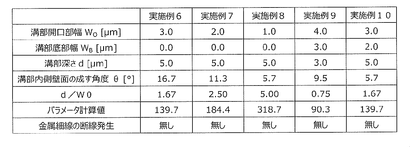
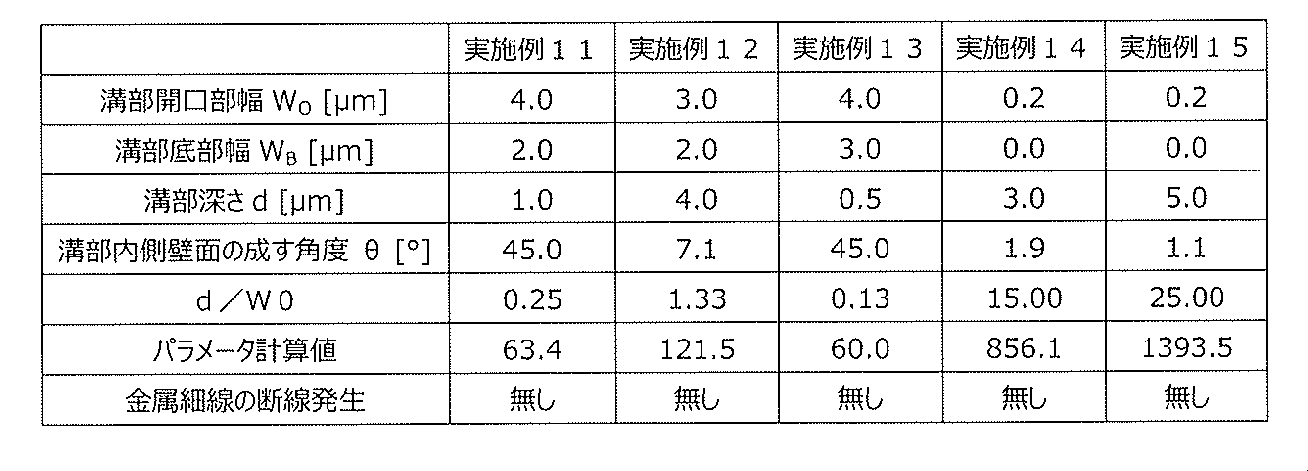


表1~表3から、実施例1~15、すなわち本発明の第1の条件~第5の条件を満たす断面形状であれば断線は発生しないことが判る。
なお、本発明に係る導電性フィルム及びタッチパネルモジュールは、上述の実施の形態に限らず、本発明の要旨を逸脱することなく、種々の構成を採り得ることはもちろんである。
16…導電性フィルム 70…フィルム部材
72…基板 74…マトリックス層
74a…土手部 74b…溝部
74c…開口部 74d…内壁側面
74e…底部 76…金属細線
72…基板 74…マトリックス層
74a…土手部 74b…溝部
74c…開口部 74d…内壁側面
74e…底部 76…金属細線
Claims (5)
- 可撓性を有するフィルム部材の表面に金属細線からなる網状の導電パターンを具える導電性フィルムにおいて、
前記金属細線が、前記フィルム部材の表面に形成された溝部に充填された金属材料からなり、
前記溝部の断面形状のうち、開口部の幅をWOとし、底部の幅をWBとし、深さをdとし、前記フィルム部材の表面と直交する方向に対する前記溝部の内壁側面の成す角度をθとすると、前記溝部が、
WO>WB
0<θ≦53.74×(d/WO)+50
0<θ≦64
0.2≦WO≦4
0.1≦d≦5という関係を満たしていることを特徴とする導電性フィルム。
但し、θの単位はdegであり、d、WO、及びWBの単位はいずれもμmである。 - 請求項1に記載の導電性フィルムにおいて、
前記溝部が前記フィルム部材に設けられたマトリックス層に形成される導電性フィルム。 - 請求項2に記載の導電性フィルムにおいて、
前記マトリックス層が光硬化性樹脂である導電性フィルム。 - 請求項1に記載の導電性フィルムにおいて、
前記金属材料がAgからなる導電性フィルム。 - 請求項1~4のいずれか1項に記載の導電性フィルムを用いたタッチパネルモジュール。
Applications Claiming Priority (2)
| Application Number | Priority Date | Filing Date | Title |
|---|---|---|---|
| JP2014070473 | 2014-03-28 | ||
| JP2014-070473 | 2014-03-28 |
Publications (1)
| Publication Number | Publication Date |
|---|---|
| WO2015146447A1 true WO2015146447A1 (ja) | 2015-10-01 |
Family
ID=54194978
Family Applications (1)
| Application Number | Title | Priority Date | Filing Date |
|---|---|---|---|
| PCT/JP2015/055507 Ceased WO2015146447A1 (ja) | 2014-03-28 | 2015-02-26 | 導電性フィルム及びタッチパネルモジュール |
Country Status (2)
| Country | Link |
|---|---|
| JP (1) | JP2015195004A (ja) |
| WO (1) | WO2015146447A1 (ja) |
Cited By (5)
| Publication number | Priority date | Publication date | Assignee | Title |
|---|---|---|---|---|
| KR101636064B1 (ko) * | 2015-02-23 | 2016-07-06 | (주)뉴옵틱스 | 터치패널용 센서시트 |
| US20160349884A1 (en) * | 2014-03-28 | 2016-12-01 | Fujifilm Corporation | Conductive film, conductive film manufacturing method, and touch panel |
| CN108351730A (zh) * | 2015-10-21 | 2018-07-31 | 微软技术许可有限责任公司 | 导电外壳中带沟槽的设备 |
| CN110032293A (zh) * | 2018-01-11 | 2019-07-19 | 夏普株式会社 | 基板、显示装置以及基板的制造方法 |
| WO2024095688A1 (ja) * | 2022-11-02 | 2024-05-10 | パナソニックIpマネジメント株式会社 | 導電フィルム |
Families Citing this family (2)
| Publication number | Priority date | Publication date | Assignee | Title |
|---|---|---|---|---|
| CN108700965A (zh) * | 2016-03-30 | 2018-10-23 | 株式会社藤仓 | 布线体、布线基板以及接触式传感器 |
| JP6641017B2 (ja) | 2016-09-12 | 2020-02-05 | 富士フイルム株式会社 | 導電性フィルム、タッチパネルセンサー、および、タッチパネル |
Citations (2)
| Publication number | Priority date | Publication date | Assignee | Title |
|---|---|---|---|---|
| JP2012155369A (ja) * | 2011-01-21 | 2012-08-16 | Japan Aviation Electronics Industry Ltd | 静電容量式タッチパネル |
| WO2013012260A2 (ko) * | 2011-07-21 | 2013-01-24 | 미래나노텍 주식회사 | 터치 스크린 패널 제조 장치 및 제조 방법 |
Family Cites Families (4)
| Publication number | Priority date | Publication date | Assignee | Title |
|---|---|---|---|---|
| KR101022015B1 (ko) * | 2010-04-09 | 2011-03-16 | 한국기계연구원 | 열형 롤 임프린팅과 블레이드 코팅을 이용하는 필름제품 제조방법, 이를 이용한 보안 필름 및 필름 일체형 전기 소자 |
| CN102222538B (zh) * | 2011-03-11 | 2012-12-05 | 苏州纳格光电科技有限公司 | 图形化的柔性透明导电薄膜及其制法 |
| CN102722279A (zh) * | 2012-05-09 | 2012-10-10 | 崔铮 | 金属网格导电层及其具备该导电层的触摸面板 |
| JP6256033B2 (ja) * | 2014-01-20 | 2018-01-10 | 大日本印刷株式会社 | タッチパネルセンサ、タッチパネルセンサの製造方法およびタッチ位置検出機能付き表示装置 |
-
2015
- 2015-02-23 JP JP2015032415A patent/JP2015195004A/ja active Pending
- 2015-02-26 WO PCT/JP2015/055507 patent/WO2015146447A1/ja not_active Ceased
Patent Citations (2)
| Publication number | Priority date | Publication date | Assignee | Title |
|---|---|---|---|---|
| JP2012155369A (ja) * | 2011-01-21 | 2012-08-16 | Japan Aviation Electronics Industry Ltd | 静電容量式タッチパネル |
| WO2013012260A2 (ko) * | 2011-07-21 | 2013-01-24 | 미래나노텍 주식회사 | 터치 스크린 패널 제조 장치 및 제조 방법 |
Cited By (5)
| Publication number | Priority date | Publication date | Assignee | Title |
|---|---|---|---|---|
| US20160349884A1 (en) * | 2014-03-28 | 2016-12-01 | Fujifilm Corporation | Conductive film, conductive film manufacturing method, and touch panel |
| KR101636064B1 (ko) * | 2015-02-23 | 2016-07-06 | (주)뉴옵틱스 | 터치패널용 센서시트 |
| CN108351730A (zh) * | 2015-10-21 | 2018-07-31 | 微软技术许可有限责任公司 | 导电外壳中带沟槽的设备 |
| CN110032293A (zh) * | 2018-01-11 | 2019-07-19 | 夏普株式会社 | 基板、显示装置以及基板的制造方法 |
| WO2024095688A1 (ja) * | 2022-11-02 | 2024-05-10 | パナソニックIpマネジメント株式会社 | 導電フィルム |
Also Published As
| Publication number | Publication date |
|---|---|
| JP2015195004A (ja) | 2015-11-05 |
Similar Documents
| Publication | Publication Date | Title |
|---|---|---|
| WO2015146447A1 (ja) | 導電性フィルム及びタッチパネルモジュール | |
| TWI559180B (zh) | 用以製造觸控螢幕面板的方法及其裝置 | |
| US9971459B2 (en) | Touch sensitive module with integrated sensor and artwork | |
| US10108304B2 (en) | Conductive film, conductive film manufacturing method, and touch panel | |
| TWI525492B (zh) | Touch panel member and manufacturing method thereof | |
| TWI395998B (zh) | 導電板及應用其之觸控板 | |
| CN106104444A (zh) | 透明导电性层叠体及具备透明导电性层叠体的触摸面板 | |
| TW201337705A (zh) | 偏光膜電阻式觸控螢幕 | |
| JP6240756B2 (ja) | タッチパネル及びその製造方法 | |
| JP2004209925A (ja) | 可とう性成形型及びその製造方法ならびにpdp用背面板及びその製造方法 | |
| US20150309620A1 (en) | Touch panel | |
| TW201611043A (zh) | 導電膜 | |
| KR101341335B1 (ko) | 터치스크린 패널 제조 장치 | |
| JP2018522377A (ja) | 回路基板の製造方法 | |
| US20150104567A1 (en) | Method for forming a functional pattern on a substrate | |
| JP2015184994A (ja) | 透明導電性積層体および透明導電性積層体を備えたタッチパネル | |
| KR101343798B1 (ko) | 터치스크린 패널 제조 방법 | |
| KR101925305B1 (ko) | 금속 나노 입자를 함유한 전도성 고분자 전극 형성 방법 및 에칭액 | |
| US20150059161A1 (en) | Touch panel producing method | |
| KR101334596B1 (ko) | 터치스크린 패널 제조 장치 | |
| JP2019008617A (ja) | 硬化膜付きタッチセンサーの製造方法及び硬化膜付きタッチセンサー | |
| JP2024033818A (ja) | 導電性フィルム、タッチセンサフィルム及び画像表示装置 | |
| KR101805614B1 (ko) | 차등선폭 전극패턴을 갖는 터치 스크린 패널 및 터치 스크린 모듈 | |
| KR20160002571A (ko) | 터치스크린 패널 제조방법 | |
| JP2015055883A (ja) | タッチパネルの製造方法及び装置 |
Legal Events
| Date | Code | Title | Description |
|---|---|---|---|
| 121 | Ep: the epo has been informed by wipo that ep was designated in this application |
Ref document number: 15770126 Country of ref document: EP Kind code of ref document: A1 |
|
| NENP | Non-entry into the national phase | ||
| 122 | Ep: pct application non-entry in european phase |
Ref document number: 15770126 Country of ref document: EP Kind code of ref document: A1 |