WO2015137446A1 - 液晶表示装置 - Google Patents
液晶表示装置 Download PDFInfo
- Publication number
- WO2015137446A1 WO2015137446A1 PCT/JP2015/057294 JP2015057294W WO2015137446A1 WO 2015137446 A1 WO2015137446 A1 WO 2015137446A1 JP 2015057294 W JP2015057294 W JP 2015057294W WO 2015137446 A1 WO2015137446 A1 WO 2015137446A1
- Authority
- WO
- WIPO (PCT)
- Prior art keywords
- optically anisotropic
- anisotropic layer
- liquid crystal
- polarizer
- crystal display
- Prior art date
- Legal status (The legal status is an assumption and is not a legal conclusion. Google has not performed a legal analysis and makes no representation as to the accuracy of the status listed.)
- Ceased
Links
Images

Classifications
-
- G—PHYSICS
- G02—OPTICS
- G02F—OPTICAL DEVICES OR ARRANGEMENTS FOR THE CONTROL OF LIGHT BY MODIFICATION OF THE OPTICAL PROPERTIES OF THE MEDIA OF THE ELEMENTS INVOLVED THEREIN; NON-LINEAR OPTICS; FREQUENCY-CHANGING OF LIGHT; OPTICAL LOGIC ELEMENTS; OPTICAL ANALOGUE/DIGITAL CONVERTERS
- G02F1/00—Devices or arrangements for the control of the intensity, colour, phase, polarisation or direction of light arriving from an independent light source, e.g. switching, gating or modulating; Non-linear optics
- G02F1/01—Devices or arrangements for the control of the intensity, colour, phase, polarisation or direction of light arriving from an independent light source, e.g. switching, gating or modulating; Non-linear optics for the control of the intensity, phase, polarisation or colour
- G02F1/13—Devices or arrangements for the control of the intensity, colour, phase, polarisation or direction of light arriving from an independent light source, e.g. switching, gating or modulating; Non-linear optics for the control of the intensity, phase, polarisation or colour based on liquid crystals, e.g. single liquid crystal display cells
- G02F1/133—Constructional arrangements; Operation of liquid crystal cells; Circuit arrangements
- G02F1/1333—Constructional arrangements; Manufacturing methods
- G02F1/1335—Structural association of cells with optical devices, e.g. polarisers or reflectors
- G02F1/13363—Birefringent elements, e.g. for optical compensation
- G02F1/133634—Birefringent elements, e.g. for optical compensation the refractive index Nz perpendicular to the element surface being different from in-plane refractive indices Nx and Ny, e.g. biaxial or with normal optical axis
-
- G—PHYSICS
- G02—OPTICS
- G02B—OPTICAL ELEMENTS, SYSTEMS OR APPARATUS
- G02B5/00—Optical elements other than lenses
- G02B5/30—Polarising elements
-
- G—PHYSICS
- G02—OPTICS
- G02F—OPTICAL DEVICES OR ARRANGEMENTS FOR THE CONTROL OF LIGHT BY MODIFICATION OF THE OPTICAL PROPERTIES OF THE MEDIA OF THE ELEMENTS INVOLVED THEREIN; NON-LINEAR OPTICS; FREQUENCY-CHANGING OF LIGHT; OPTICAL LOGIC ELEMENTS; OPTICAL ANALOGUE/DIGITAL CONVERTERS
- G02F1/00—Devices or arrangements for the control of the intensity, colour, phase, polarisation or direction of light arriving from an independent light source, e.g. switching, gating or modulating; Non-linear optics
- G02F1/01—Devices or arrangements for the control of the intensity, colour, phase, polarisation or direction of light arriving from an independent light source, e.g. switching, gating or modulating; Non-linear optics for the control of the intensity, phase, polarisation or colour
- G02F1/13—Devices or arrangements for the control of the intensity, colour, phase, polarisation or direction of light arriving from an independent light source, e.g. switching, gating or modulating; Non-linear optics for the control of the intensity, phase, polarisation or colour based on liquid crystals, e.g. single liquid crystal display cells
- G02F1/133—Constructional arrangements; Operation of liquid crystal cells; Circuit arrangements
- G02F1/1333—Constructional arrangements; Manufacturing methods
- G02F1/1335—Structural association of cells with optical devices, e.g. polarisers or reflectors
- G02F1/13363—Birefringent elements, e.g. for optical compensation
- G02F1/133633—Birefringent elements, e.g. for optical compensation using mesogenic materials
-
- G—PHYSICS
- G02—OPTICS
- G02F—OPTICAL DEVICES OR ARRANGEMENTS FOR THE CONTROL OF LIGHT BY MODIFICATION OF THE OPTICAL PROPERTIES OF THE MEDIA OF THE ELEMENTS INVOLVED THEREIN; NON-LINEAR OPTICS; FREQUENCY-CHANGING OF LIGHT; OPTICAL LOGIC ELEMENTS; OPTICAL ANALOGUE/DIGITAL CONVERTERS
- G02F1/00—Devices or arrangements for the control of the intensity, colour, phase, polarisation or direction of light arriving from an independent light source, e.g. switching, gating or modulating; Non-linear optics
- G02F1/01—Devices or arrangements for the control of the intensity, colour, phase, polarisation or direction of light arriving from an independent light source, e.g. switching, gating or modulating; Non-linear optics for the control of the intensity, phase, polarisation or colour
- G02F1/13—Devices or arrangements for the control of the intensity, colour, phase, polarisation or direction of light arriving from an independent light source, e.g. switching, gating or modulating; Non-linear optics for the control of the intensity, phase, polarisation or colour based on liquid crystals, e.g. single liquid crystal display cells
- G02F1/133—Constructional arrangements; Operation of liquid crystal cells; Circuit arrangements
- G02F1/1333—Constructional arrangements; Manufacturing methods
- G02F1/1335—Structural association of cells with optical devices, e.g. polarisers or reflectors
- G02F1/13363—Birefringent elements, e.g. for optical compensation
- G02F1/133637—Birefringent elements, e.g. for optical compensation characterised by the wavelength dispersion
-
- G—PHYSICS
- G02—OPTICS
- G02F—OPTICAL DEVICES OR ARRANGEMENTS FOR THE CONTROL OF LIGHT BY MODIFICATION OF THE OPTICAL PROPERTIES OF THE MEDIA OF THE ELEMENTS INVOLVED THEREIN; NON-LINEAR OPTICS; FREQUENCY-CHANGING OF LIGHT; OPTICAL LOGIC ELEMENTS; OPTICAL ANALOGUE/DIGITAL CONVERTERS
- G02F1/00—Devices or arrangements for the control of the intensity, colour, phase, polarisation or direction of light arriving from an independent light source, e.g. switching, gating or modulating; Non-linear optics
- G02F1/01—Devices or arrangements for the control of the intensity, colour, phase, polarisation or direction of light arriving from an independent light source, e.g. switching, gating or modulating; Non-linear optics for the control of the intensity, phase, polarisation or colour
- G02F1/13—Devices or arrangements for the control of the intensity, colour, phase, polarisation or direction of light arriving from an independent light source, e.g. switching, gating or modulating; Non-linear optics for the control of the intensity, phase, polarisation or colour based on liquid crystals, e.g. single liquid crystal display cells
- G02F1/133—Constructional arrangements; Operation of liquid crystal cells; Circuit arrangements
- G02F1/1333—Constructional arrangements; Manufacturing methods
- G02F1/1337—Surface-induced orientation of the liquid crystal molecules, e.g. by alignment layers
- G02F1/133742—Surface-induced orientation of the liquid crystal molecules, e.g. by alignment layers for homeotropic alignment
-
- G—PHYSICS
- G02—OPTICS
- G02F—OPTICAL DEVICES OR ARRANGEMENTS FOR THE CONTROL OF LIGHT BY MODIFICATION OF THE OPTICAL PROPERTIES OF THE MEDIA OF THE ELEMENTS INVOLVED THEREIN; NON-LINEAR OPTICS; FREQUENCY-CHANGING OF LIGHT; OPTICAL LOGIC ELEMENTS; OPTICAL ANALOGUE/DIGITAL CONVERTERS
- G02F2413/00—Indexing scheme related to G02F1/13363, i.e. to birefringent elements, e.g. for optical compensation, characterised by the number, position, orientation or value of the compensation plates
- G02F2413/04—Number of plates greater than or equal to 4
-
- G—PHYSICS
- G02—OPTICS
- G02F—OPTICAL DEVICES OR ARRANGEMENTS FOR THE CONTROL OF LIGHT BY MODIFICATION OF THE OPTICAL PROPERTIES OF THE MEDIA OF THE ELEMENTS INVOLVED THEREIN; NON-LINEAR OPTICS; FREQUENCY-CHANGING OF LIGHT; OPTICAL LOGIC ELEMENTS; OPTICAL ANALOGUE/DIGITAL CONVERTERS
- G02F2413/00—Indexing scheme related to G02F1/13363, i.e. to birefringent elements, e.g. for optical compensation, characterised by the number, position, orientation or value of the compensation plates
- G02F2413/06—Two plates on one side of the LC cell
-
- G—PHYSICS
- G02—OPTICS
- G02F—OPTICAL DEVICES OR ARRANGEMENTS FOR THE CONTROL OF LIGHT BY MODIFICATION OF THE OPTICAL PROPERTIES OF THE MEDIA OF THE ELEMENTS INVOLVED THEREIN; NON-LINEAR OPTICS; FREQUENCY-CHANGING OF LIGHT; OPTICAL LOGIC ELEMENTS; OPTICAL ANALOGUE/DIGITAL CONVERTERS
- G02F2413/00—Indexing scheme related to G02F1/13363, i.e. to birefringent elements, e.g. for optical compensation, characterised by the number, position, orientation or value of the compensation plates
- G02F2413/12—Biaxial compensators
Definitions
- the present invention relates to a liquid crystal display device having a vertical alignment mode liquid crystal cell.
- liquid crystal display devices have been made thinner, and accordingly, members (for example, polarizing plates) used are required to be made thinner.
- members for example, polarizing plates
- a method of thinning the polarizing plate for example, a method of thinning the polarizer itself or the protective film of the polarizer, a method of eliminating the protective film or retardation film disposed between the polarizer and the liquid crystal cell, etc. Can be mentioned.
- Patent Document 1 discloses that “a liquid crystal cell having a liquid crystal layer that is vertically aligned with respect to a substrate during black display, and an absorption axis of each of the liquid crystal cells sandwiching each other.
- a liquid crystal display device having two polarizers arranged orthogonally and a retardation film arranged between each of the two polarizers and a liquid crystal cell and having the same optical anisotropy
- the liquid crystal display device wherein the retardation film contains cellulose acylate and a liquid crystal compound, and satisfies the following formulas (I) to (IV).
- the inventors of the present invention have studied the liquid crystal display device described in Patent Document 1, and have improved color change (color shift) and light leakage (black luminance) that occur when the liquid crystal cell is observed from an oblique direction. It has been clarified that there is room and display unevenness may occur due to changes in the temperature and humidity environment.
- the present invention provides a liquid crystal display that is excellent in display performance (prevention of color change and light leakage) even when it is thinned, and excellent in durability against temperature / humidity change (performance of suppressing display unevenness). It is an object to provide an apparatus.
- the inventors of the present invention have performed optical compensation of the vertical alignment mode liquid crystal cell with two optical anisotropies (one on the viewing side and one on the backlight side) having desired optical characteristics.
- the liquid crystal display device is thinned by securing the optical compensation of each of the viewing side polarizer and the backlight side polarizer with an optically anisotropic layer having desired optical characteristics. Even if it exists, it discovered that it was excellent in display performance and the durability with respect to a temperature / humidity environmental change, and completed this invention. That is, it has been found that the above object can be achieved by the following configuration.
- the polarizer (P1) and the polarizer (P2) are arranged with their respective absorption axes orthogonal to each other,
- the thickness of each of the optically anisotropic layer (C1) and the optically anisotropic layer (C2) is 10 ⁇ m or less,
- the optically anisotropic layer (C1) and the optically anisotropic layer (C2) both satisfy the following formulas (1-1) and (1-2), Re (550) ⁇ 30 nm Formula (1-1) 10 nm ⁇ Rth (550) ⁇ 100 nm Formula (1-2)
- the optically anisotropic layer (B1) and the optically anisotropic layer (B2) are all represented by the following formulas (1-3), (1-4), (1-5), (1-6) and (1- The liquid crystal display device satisfying 7).
- the first polarizer (P1), the optically anisotropic layer (C1) having the first liquid crystalline compound, and the first optically anisotropic layer (B1) A vertical alignment mode liquid crystal cell, a second optically anisotropic layer (B2), an optically anisotropic layer (C2) having a second liquid crystalline compound, and a second polarizer (P2) in this order.
- the polarizer (P1) and the polarizer (P2) are arranged with their respective absorption axes orthogonal to each other,
- the thickness of each of the optically anisotropic layer (C1) and the optically anisotropic layer (C2) is 10 ⁇ m or less,
- the optically anisotropic layer (C1) and the optically anisotropic layer (C2) both satisfy the following formulas (2-1) and (2-2), Re (550) ⁇ 30 nm Formula (2-1) 30 nm ⁇ Rth (550) ⁇ 120 nm Formula (2-2)
- the first polarizer (P1), the optically anisotropic layer (A1) having the first liquid crystalline compound, and the first optically anisotropic layer (C1) A vertical alignment mode liquid crystal cell, a second optically anisotropic layer (C2), an optically anisotropic layer (A2) having a second liquid crystalline compound, and a second polarizer (P2) in this order.
- the polarizer (P1) and the polarizer (P2) are arranged with their respective absorption axes orthogonal to each other,
- the thicknesses of the optically anisotropic layer (A1) and the optically anisotropic layer (A2) are both 10 ⁇ m or less,
- the optically anisotropic layer (A1) and the optically anisotropic layer (A2) all satisfy the following formulas (3-1), (3-2) and (3-3), 50 nm ⁇ Re (550) ⁇ 130 Formula (3-1) 20 nm ⁇ Rth (550) ⁇ 70 Formula (3-2) Re (450) / Re (550) ⁇ 1.05 Formula (3-3)
- the polarizer (P1) and the polarizer (P2) are arranged with their respective absorption axes orthogonal to each other,
- the thicknesses of the optically anisotropic layer (A1) and the optically anisotropic layer (A2) are both 10 ⁇ m or less,
- the optically anisotropic layer (A1) and the optically anisotropic layer (A2) all satisfy the following formulas (4-1), (4-2) and (4-3), 10 nm ⁇ Re (550) ⁇ 70 nm Formula (4-1) 0 nm ⁇ Rth (550) ⁇ 40 nm Formula (4-2) Re (450) / Re (550) ⁇ 1.05 Formula (4-3)
- the liquid crystalline compounds contained in the optically anisotropic layer (C1) and the optically anisotropic layer (C2) are both discotic liquid crystalline compounds,
- the polarizer (P1) and the optically anisotropic layer (C1) are stacked via the alignment film, and the polarizer (P2) and the optically anisotropic layer (C2) are stacked via the alignment film.
- the polarizer (P1) and the optically anisotropic layer (A1) are stacked via the alignment film, and the polarizer (P2) and the optically anisotropic layer (A2) are stacked via the alignment film.
- the polarizer (P1) and the optically anisotropic layer (C1) are laminated via an adhesive layer or an adhesive layer, and the polarizer (P2) and the optically anisotropic layer (C2) are adhesives.
- the liquid crystal display device according to [2] which is laminated via a layer or an adhesive layer.
- the polarizer (P1) and the optically anisotropic layer (A1) are laminated via an adhesive layer or an adhesive layer, and the polarizer (P2) and the optically anisotropic layer (A2) are adhesives.
- a protective film is provided on one or both of the viewing side of the polarizer (P1) and the backlight side of the polarizer (P2), Moisture permeability of the protective film is not more than 100g / m 2 / 24h, a liquid crystal display device according to any one of [1] to [14].
- the water vapor permeability of at least one optically anisotropic layer selected from the group consisting of the optically anisotropic layer (C2) is 50 g / m 2 / 24h or less, and any one of [1] to [15] Liquid crystal display device.
- a laminate film is provided on one or both of the viewing side of the polarizer (P1) and the backlight side of the polarizer (P2), Moisture permeability of the laminated film is not more than 30g / m 2 / 24h, a liquid crystal display device according to any one of [1] to [14].
- liquid crystal display device that is excellent in display performance even when it is thinned and excellent in durability against changes in temperature and humidity environment.
- FIGS. 3A to 3C are schematic cross-sectional views each showing an example of the third aspect of the liquid crystal display device of the present invention.
- 4A to 4C are schematic cross-sectional views showing examples of the fourth aspect of the liquid crystal display device of the present invention.
- Re ( ⁇ ) and Rth ( ⁇ ) represent in-plane retardation and retardation in the thickness direction at the wavelength ⁇ , respectively.
- Re ( ⁇ ) is measured by making light having a wavelength of ⁇ nm incident in the normal direction of the film in KOBRA 21ADH or KOBRA WR (both manufactured by Oji Scientific Instruments). In selecting the measurement wavelength ⁇ nm, the wavelength selection filter can be exchanged manually, or the measurement value can be converted by a program or the like.
- Rth ( ⁇ ) is calculated by the following method.
- Rth ( ⁇ ) is Re ( ⁇ ) with the in-plane slow axis (determined by KOBRA 21ADH or KOBRA WR) as the tilt axis (rotation axis) (in the absence of the slow axis,
- the light of wavelength ⁇ nm is incident from each inclined direction in steps of 10 degrees from the normal direction to 50 degrees on one side, and a total of 6 points are measured.
- the KOBRA 21ADH or KOBRA WR is calculated based on the measured retardation value, the assumed value of the average refractive index, and the input film thickness value. In the above case, in the case of a film having a direction in which the retardation value is zero at a certain tilt angle with the in-plane slow axis from the normal direction as the rotation axis, retardation at a tilt angle larger than the tilt angle. The value is calculated in KOBRA 21ADH or KOBRA WR after changing its sign to negative.
- the retardation value is measured from the two inclined directions, with the slow axis as the tilt axis (rotation axis) (when there is no slow axis, the arbitrary direction in the film plane is the rotation axis), Based on the value, the assumed value of the average refractive index, and the input film thickness value, Rth can also be calculated from the following formulas (1) and (2).
- Re ( ⁇ ) represents a retardation value in a direction inclined by an angle ⁇ from the normal direction.
- nx represents the refractive index in the slow axis direction in the plane
- ny represents the refractive index in the direction perpendicular to nx in the plane
- nz represents the refractive index in the direction perpendicular to nx and ny.
- d represents the film thickness of the film.
- Rth ( ⁇ ) is calculated by the following method.
- Rth ( ⁇ ) is -50 ° to + 50 ° with respect to the film normal direction with Re ( ⁇ ) being the in-plane slow axis (determined by KOBRA 21ADH or KOBRA WR) as the tilt axis (rotation axis) 11 points of light having a wavelength of ⁇ nm are incident from each inclined direction in 10 degree steps until KOBRA 21ADH is measured based on the measured retardation value, assumed average refractive index, and input film thickness value. Or it is calculated by KOBRA WR.
- Re40 ( ⁇ ) represents retardation measured from a polar angle of 40 ° at a wavelength ⁇ nm.
- the angle relationship (for example, “orthogonal”, “parallel”, “90 °”, etc.) includes a range of errors allowed in the technical field to which the present invention belongs. Specifically, it means that the angle is within a range of strict angle ⁇ 10 °, and an error from the strict angle is preferably 5 ° or less, and more preferably 3 ° or less.
- moisture permeability refers to a sample in an atmosphere at a temperature of 40 ° C. and a relative humidity of 90% in accordance with the method described in “Moisture permeability test method for moisture-proof packaging materials (cup method)” of JIS Z 0208: 1976. Is the amount (g / m 2 / day) converted per 1 m 2 of area by measuring the mass of water vapor that passes through 24 hours.
- the liquid crystal display device of the present invention includes a vertical alignment mode liquid crystal cell and two polarizers (polarizers (P1) and (P2 described later) arranged with the absorption axes perpendicular to each other across the liquid crystal cell. )).
- the first polarizer (P1), the first optical anisotropic layer (B1), the first in the direction from the viewing side to the backlight side.
- the liquid crystal display device has the second polarizer (P2) in this order and satisfies the above-described formulas (1-1) to (1-7).
- the liquid crystal display device includes a first polarizer (P1), an optically anisotropic layer (C1) having a first liquid crystalline compound, a first liquid crystal compound in the direction from the viewing side to the backlight side.
- a first polarizer (P1) an optically anisotropic layer (C1) having a first liquid crystalline compound, a first liquid crystal compound in the direction from the viewing side to the backlight side.
- the liquid crystal display device includes a first polarizer (P1), an optically anisotropic layer (A1) having a first liquid crystalline compound, a first liquid crystal compound in the direction from the viewer side to the backlight side.
- a first polarizer (P1) an optically anisotropic layer (A1) having a first liquid crystalline compound, a first liquid crystal compound in the direction from the viewer side to the backlight side.
- the liquid crystal display device includes a first polarizer (P1), a first optically anisotropic layer (C1), and a first liquid crystalline compound in the direction from the viewing side to the backlight side.
- This is a liquid crystal display device having the polarizers (P2) in this order and satisfying the above-mentioned formulas (4-1) to (4-5).
- the optical compensation of the vertical alignment mode liquid crystal cell is performed by the optical anisotropic layers (C1) and (C2) arranged with the liquid crystal cell interposed therebetween, and the optical compensation of each of the polarizers (P1) and (P2). This is considered to be because the optical compensation function could be appropriately separated by performing the steps in the optically anisotropic layers (B1) and (B2) or the optically anisotropic layers (A1) and (A2). .
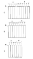
- FIG. 1 is a schematic cross-sectional view showing an example of a liquid crystal display device according to the first aspect of the present invention.
- a liquid crystal display device 40 shown in FIG. 1A includes a first polarizer (P1) 1, a first optically anisotropic layer (B1) 2, and a first liquid crystal in the direction from the viewing side to the backlight side.
- P1 first polarizer
- B1 first optically anisotropic layer
- the liquid crystal display device 40 shown in FIG. 1B has an arbitrary protective film 4 on the viewing side of the polarizer (P1) 1 of the liquid crystal display device shown in FIG. 1A, and the polarizer (P2). 11 has an optional protective film 14 on the backlight side.
- the optional protective film is provided only on one of the viewing side of the polarizer (P1) 1 and the backlight side of the polarizer (P2) 11 separately from the embodiment shown in FIG. Also good.
- the liquid crystal display device 40 in FIG. 1C has an arbitrary laminate film 5 on the viewing side of the protective film 4 of the liquid crystal display device shown in FIG. In this embodiment, the laminate film 15 is provided.
- the arbitrary laminated film may have only in any one of the visual recognition side of the protective film 4, and the backlight side of the protective film 14 separately from the aspect shown to FIG. You may have in the aspect which does not have a film
- symbol 10 shows the visual recognition side polarizing plate
- symbol 30 shows a backlight side polarizing plate.
- the optically anisotropic layer (C1) and the optically anisotropic layer (C2) both satisfy the following formulas (1-1) and (1-2), and
- the optically anisotropic layer (B1) and the optically anisotropic layer (B2) are all represented by the following formulas (1-3), (1-4), (1-5), (1-6) and (1- This is a mode that satisfies 7).
- the optically anisotropic layer (C1) and the optically anisotropic layer (C2) are more reduced in light leakage (black luminance) generated when observed from an oblique direction.
- Re (550) is preferably 20 nm or less, more preferably 10 nm or less
- Rth (550) is 20 nm to 90 nm for the reason that the display performance is better.
- the thickness is preferably 25 nm to 80 nm.
- the optically anisotropic layer (B1) and the optically anisotropic layer (B2) are further suppressed in light leakage (black luminance) generated when observed from an oblique direction, and display performance even when the thickness is reduced.
- Re (550) is preferably 35 nm to 140 nm, more preferably 45 nm to 120 nm, Rth (550) is preferably 30 nm to 120 nm, and 40 nm to 100 nm. More preferably. Furthermore, the color change (color shift) that occurs when observed from an oblique direction is further suppressed, and even when the thickness is reduced, the display performance is better. Therefore, Re (450) / Re (550) is 1. 0.0 or less is preferable, and 0.95 or less is more preferable.
- the thicknesses of the optically anisotropic layer (C1) and the optically anisotropic layer (C2) having a liquid crystal compound are both 10 ⁇ m or less, preferably 7 ⁇ m or less, More preferably, it is 5 ⁇ m or less.
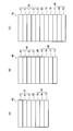
- FIG. 2 is a schematic cross-sectional view showing an example of a liquid crystal display device according to the second aspect of the present invention.
- a liquid crystal display device 40 shown in FIG. 2A includes an optically anisotropic layer (C1) 3 having a first polarizer (P1) 1 and a first liquid crystal compound in the direction from the viewing side to the backlight side.
- C1 3 optically anisotropic layer
- P1 1 first polarizer
- 2B has an optional protective film 4 on the viewing side of the polarizer (P1) 1 of the liquid crystal display device shown in FIG. 2A, and the polarizer (P2). 11 has an optional protective film 14 on the backlight side.
- the optional protective film is provided only on one of the viewing side of the polarizer (P1) 1 and the backlight side of the polarizer (P2) 11 separately from the embodiment shown in FIG. Also good.
- the liquid crystal display device 40 in FIG. 2C has an arbitrary laminate film 5 on the viewing side of the protective film 4 of the liquid crystal display device shown in FIG. In this embodiment, the laminate film 15 is provided.
- the arbitrary laminated film may have only in any one of the visual recognition side of the protective film 4, and the backlight side of the protective film 14 separately from the aspect shown to FIG. You may have in the aspect which does not have a film
- symbol 10 shows the visual recognition side polarizing plate
- symbol 30 shows a backlight side polarizing plate.
- the optically anisotropic layer (C1) and the optically anisotropic layer (C2) both satisfy the following formulas (2-1) and (2-2), and
- the optically anisotropic layer (B1) and the optically anisotropic layer (B2) all satisfy the following formulas (2-3), (2-4) and (2-5).
- the optically anisotropic layer (C1) and the optically anisotropic layer (C2) are further reduced in light leakage (black luminance) generated when observed from an oblique direction.
- Re (550) is preferably 20 nm or less, more preferably 10 nm or less, and Rth (550) is 35 nm to 110 nm because the display performance is better.
- the thickness is preferably 40 nm to 100 nm.
- the optically anisotropic layer (B1) and the optically anisotropic layer (B2) are further suppressed in light leakage (black luminance) generated when observed from an oblique direction, and display performance even when the thickness is reduced.
- Re (550) is preferably 20 nm to 65 nm, more preferably 25 nm to 60 nm, Rth (550) is preferably 30 nm to 100 nm, and 40 nm to 90 nm. More preferably. Furthermore, the color change (color shift) that occurs when observed from an oblique direction is further suppressed, and even when the thickness is reduced, the display performance is better. Therefore, Re (450) / Re (550) is 1. 0.0 or less is preferable, and 0.95 or less is more preferable.
- the thicknesses of the optically anisotropic layer (C1) and the optically anisotropic layer (C2) having a liquid crystal compound are both 10 ⁇ m or less, preferably 7 ⁇ m or less, More preferably, it is 5 ⁇ m or less.
- the liquid crystal display device can be made thinner, and the optical property having the polarizer (P1) and the liquid crystal compound is improved because the durability against changes in temperature and humidity environment is further improved.
- the optical property having the polarizer (P1) and the liquid crystal compound is improved because the durability against changes in temperature and humidity environment is further improved.
- Laminated structure; the polarizer (P1) and the optically anisotropic layer (C1) are interposed via an adhesive layer or a pressure-sensitive adhesive layer. Is a layer, a polarizer (P2) and the optically anisotropic layer (C2) and is configured are laminated through an adhesive layer or a pressure-sensitive adhesive layer; preferably the like.
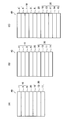
- FIG. 3 is a schematic cross-sectional view showing an example of a liquid crystal display device according to the third aspect of the present invention.
- the liquid crystal display device 40 shown in FIG. 3A includes an optically anisotropic layer (A1) 6 having a first polarizer (P1) 1 and a first liquid crystalline compound in the direction from the viewing side to the backlight side.
- A1 6 optically anisotropic layer having a first polarizer (P1) 1 and a first liquid crystalline compound in the direction from the viewing side to the backlight side.
- 3B has an optional protective film 4 on the viewing side of the polarizer (P1) 1 of the liquid crystal display device shown in FIG. 3A, and the polarizer (P2). 11 has an optional protective film 14 on the backlight side.
- the optional protective film is provided only on either the viewing side of the polarizer (P1) 1 or the backlight side of the polarizer (P2) 11 separately from the embodiment shown in FIG. Also good.
- the liquid crystal display device 40 in FIG. 3C has an arbitrary laminate film 5 on the viewing side of the protective film 4 of the liquid crystal display device shown in FIG. In this embodiment, the laminate film 15 is provided.
- the arbitrary laminated film may have only in any one of the visual recognition side of the protective film 4, and the backlight side of the protective film 14 separately from the aspect shown to FIG. You may have in the aspect which does not have a film
- symbol 10 shows the visual recognition side polarizing plate
- symbol 30 shows a backlight side polarizing plate.
- the optically anisotropic layer (A1) and the optically anisotropic layer (A2) are all represented by the following formulas (3-1), (3-2) and (3-3):
- the optically anisotropic layer (C1) and the optically anisotropic layer (C2) both satisfy the following formulas (3-4) and (3-5).
- the optically anisotropic layer (A1) and the optically anisotropic layer (A2) are further reduced in light leakage (black luminance) generated when observed from an oblique direction.
- Re (550) is preferably from 60 nm to 120 nm, more preferably from 70 nm to 110 nm, and Rth (550) is from 30 nm to 60 nm, for the reason that the display performance is even better.
- the thickness is preferably 35 nm to 55 nm. Furthermore, the color change (color shift) that occurs when observed from an oblique direction is further suppressed, and even when the thickness is reduced, the display performance is better. Therefore, Re (450) / Re (550) is 1.
- Re (550) is preferably 20 nm or less, more preferably 10 nm or less, and Rth (550) is preferably 30 nm to 100 nm, and preferably 40 nm to 90 nm. Is more preferable.
- the thicknesses of the optically anisotropic layer (A1) and the optically anisotropic layer (A2) having a liquid crystal compound are both 10 ⁇ m or less, preferably 7 ⁇ m or less, More preferably, it is 5 ⁇ m or less.
- the liquid crystal display device can be made thinner, and the durability against changes in the temperature and humidity environment can be further improved.
- the polarizer (P1) and the optically anisotropic layer (A1) are adjacent to each other, and the polarizer (P2) and the optically anisotropic layer (A2) are adjacent to each other ( 3)
- the polarizer (P1) and the optically anisotropic layer (A1) are laminated via the alignment film
- the polarizer (P2) and the optically anisotropic layer (A2) are interposed via the alignment film.
- Laminated structure; the polarizer (P1) and the optically anisotropic layer (A1) are interposed via an adhesive layer or a pressure-sensitive adhesive layer.
- Is a layer, a polarizer (P2) and the optically anisotropic layer (A2) and is configured are laminated through an adhesive layer or a pressure-sensitive adhesive layer; preferably the like.
- FIG. 4 is a schematic cross-sectional view showing an example of a liquid crystal display device according to the first aspect of the present invention.
- a liquid crystal display device 40 shown in FIG. 4A includes a first polarizer (P1) 1, a first optical anisotropic layer (C1) 3, and a first liquid crystal in the direction from the viewing side to the backlight side.
- P1 first polarizer
- C1 first optical anisotropic layer
- a liquid crystal display device 40 shown in FIG. 4B has an optional protective film 4 on the viewing side of the polarizer (P1) 1 of the liquid crystal display device shown in FIG. 4A, and the polarizer (P2). 11 has an optional protective film 14 on the backlight side.
- the optional protective film is provided only on either the viewing side of the polarizer (P1) 1 or the backlight side of the polarizer (P2) 11 separately from the embodiment shown in FIG. Also good.
- the liquid crystal display device 40 in FIG. 4C has an arbitrary laminate film 5 on the viewing side of the protective film 4 of the liquid crystal display device shown in FIG. In this embodiment, the laminate film 15 is provided.
- the arbitrary laminated film may have only in any one of the visual recognition side of the protective film 4, and the backlight side of the protective film 14 separately from the aspect shown in FIG.4 (C), and protection.
- the optically anisotropic layer (A1) and the optically anisotropic layer (A2) are all represented by the following formulas (4-1), (4-2), and (4-3).
- the optically anisotropic layer (C1) and the optically anisotropic layer (C2) both satisfy the following formulas (4-4) and (4-5).
- the optically anisotropic layer (A1) and the optically anisotropic layer (A2) are further reduced in light leakage (black luminance) generated when observed from an oblique direction.
- Re (550) is preferably 15 nm to 60 nm, more preferably 20 nm to 50 nm, and Rth (550) is 5 nm to 30 nm for the reason that display performance is better.
- the thickness is preferably 10 nm to 25 nm. Furthermore, the color change (color shift) that occurs when observed from an oblique direction is further suppressed, and even when the thickness is reduced, the display performance is better. Therefore, Re (450) / Re (550) is 1.
- Re (550) is preferably 20 nm or less, more preferably 10 nm or less, and Rth (550) is preferably 80 nm to 160 nm, and 90 nm to 140 nm. Is more preferable.
- the thicknesses of the optically anisotropic layer (A1) and the optically anisotropic layer (A2) having a liquid crystal compound are both 10 ⁇ m or less, preferably 7 ⁇ m or less, More preferably, it is 5 ⁇ m or less.
- first and second modes (common)
- light leakage black luminance
- color change color shift
- display performance is improved even when the thickness is reduced.
- the liquid crystalline compounds contained in the optically anisotropic layer (C1) and the optically anisotropic layer (C2) described above are both discotic liquid crystalline compounds described later, and are optically anisotropic.
- both the functional layer (C1) and the optically anisotropic layer (C2) satisfy the following formula (5), more preferably the following formula (5-1), and the following formula (5-2): It is further preferable to satisfy 0.9 ⁇ Re40 (450) / Re40 (550) ⁇ 1.2 Formula (5) 0.95 ⁇ Re40 (450) / Re40 (550) ⁇ 1.19 Formula (5-1) 0.99 ⁇ Re40 (450) / Re40 (550) ⁇ 1.18 Formula (5-2)
- the optically anisotropic layer (B1) and the optically anisotropic layer (B2) described above are both optically anisotropic layers including a polymer film described later. It is preferable.
- the optically anisotropic layer (C1) and the optically anisotropic layer (C2) both contain a discotic liquid crystalline compound described later, and the optically anisotropic layer (C1) and optical
- the anisotropic layer (C2) preferably satisfies the following formula (5), more preferably satisfies the following formula (5-1), and further preferably satisfies the following formula (5-2).
- the light leakage (black luminance) and the color change (color shift) that occur when observed from an oblique direction are further suppressed, and even when the display is thinned, the display performance
- the liquid crystal compound contained in the optically anisotropic layer (A1) and the optically anisotropic layer (A2) is preferably a rod-like liquid crystal compound described later.
- both the optically anisotropic layer (A1) and the optically anisotropic layer (A2) preferably satisfy the following formula (6), and more preferably satisfy the following formula (6-1). More preferably, the following formula (6-2) is satisfied.
- the optically anisotropic layer (C1) and the optically anisotropic layer (C2) are optically anisotropic including a polymer film in addition to the preferred embodiment having a liquid crystalline compound. It may be a sex layer.
- optically anisotropic layer > ⁇ Liquid crystal compound ⁇
- the optically anisotropic layers (C1) and (C2) according to the first and second embodiments are layers having a liquid crystal compound, and preferably contain a discotic liquid crystal compound as described above.
- the optically anisotropic layers (C1) and (C2) according to the third and fourth aspects are preferably layers containing a discotic liquid crystalline compound as described above.
- the optically anisotropic layer (A1) and the optically anisotropic layer (A2) according to the third and fourth aspects are layers having a liquid crystal compound, and contain a rod-like liquid crystal compound as described above. It is preferable.
- liquid crystalline compound various known discotic liquid crystalline compounds and rod-shaped liquid crystalline compounds can be used as the liquid crystalline compound.
- the liquid crystalline compound includes those that no longer exhibit liquid crystallinity due to polymerization or the like.
- discotic liquid crystalline compound Various known compounds can be used for the discotic liquid crystalline compound used in the present invention.
- Examples of discotic liquid crystalline compounds include C.I. Destrade et al., Mol. Cryst. 71, 111 (1981), benzene derivatives described in C.I. Destrade et al., Mol. Cryst. 122, 141 (1985), Physics lett, A, 78, 82 (1990); Kohne et al., Angew. Chem. 96, page 70 (1984) and the cyclohexane derivatives described in J. Am. M.M. Lehn et al. Chem. Commun. 1794 (1985), J. Am. Zhang et al., J.
- the optically anisotropic layer (for example, the optically anisotropic layer (C1) described above) satisfies the following formula (5) as described above.
- the following formula (5-1) is satisfied, and it is more preferable that the following formula (5-2) is satisfied.
- Formula (5) 0.95 ⁇ Re40 (450) / Re40 (550) ⁇ 1.19
- Formula (5-1) 0.99 ⁇ Re40 (450) / Re40 (550) ⁇ 1.18 Formula (5-2)
- rod-like liquid crystal compound used in the present invention Various known compounds can be used as the rod-like liquid crystal compound used in the present invention.
- rod-like liquid crystalline compounds include azomethines, azoxys, cyanobiphenyls, cyanophenyl esters, benzoic acid esters, cyclohexanecarboxylic acid phenyl esters, cyanophenylcyclohexanes, cyano-substituted phenylpyrimidines, alkoxy-substituted phenylpyrimidines.
- Phenyldioxanes, tolanes and alkenylcyclohexylbenzonitriles are preferably used.
- those described in [0025] to [0183] of International Publication No. 2013/018526 can be used.
- the optically anisotropic layer (for example, the above-described optically anisotropic layer (A1)) preferably satisfies the following formula (6). It is more preferable to satisfy 6-1), and it is even more preferable to satisfy the following formula (6-2).
- ⁇ Boronic acid compound> when an optically anisotropic layer containing a liquid crystalline compound is directly formed on the polarizer, in order to improve the adhesion between the polarizer and the optically anisotropic layer, the optically anisotropic layer is combined with the liquid crystalline compound.
- Boronic acid compounds may be used.
- Examples of the boronic acid compound that can be used in the present invention represent a compound having at least one boronic acid group or a boronic ester group, and a metal complex or tetracoordinate having these as a ligand.
- the boron atoms having boron atoms are also represented at the same time, and those described in JP2013-05201A, paragraph numbers [0040] to [0053] can be used.
- a preferable range of the content of the boronic acid compound in the optically anisotropic layer is 0.005 to in the optically anisotropic layer (in the composition before layer formation, in the total solid content excluding the solvent of the composition).
- the content is preferably 8% by mass, more preferably 0.01 to 5% by mass, and still more preferably 0.05 to 1% by mass.
- the optically anisotropic layer (B1) and the optically anisotropic layer (B2) according to the first and second aspects are preferably optically anisotropic layers including a polymer film.
- the optically anisotropic layer (C1) and the optically anisotropic layer (C2) according to the third and fourth aspects may be optically anisotropic layers including a polymer film.
- polymer films can be used as the polymer film used in the present invention, and specific examples include cellulose acylate films, (meth) acrylic resin films, polyester resin films, and cycloolefin resin films. It is done.
- the thickness of the polymer film is preferably 250 ⁇ m or less, more preferably 200 ⁇ m or less, and even more preferably 150 ⁇ m or less. Although a minimum is not specifically limited, Generally it is 10 micrometers or more.
- the moisture permeability at a temperature 40 ° C. and 90% relative humidity is not more than 50g / m 2 / 24h of the polymeric film, 40 g / m more preferably 2 / 24h or less, and more preferably not more than 30g / m 2 / 24h.
- the polymer film having moisture permeability satisfying this value include (meth) acrylic resin film, polyester resin film, cycloolefin resin film, and the like.
- the (meth) acrylic resin is a concept including both a methacrylic resin and an acrylic resin, and includes an acrylate / methacrylate derivative, particularly an acrylate ester / methacrylate ester (co) polymer. Further, the (meth) acrylic resin includes, in addition to the methacrylic resin and acrylic resin, a (meth) acrylic polymer having a ring structure in the main chain, a polymer having a lactone ring, and a succinic anhydride ring. A maleic anhydride-based polymer having, a polymer having a glutaric anhydride ring, and a glutarimide ring-containing polymer.
- Polyester resins are preferably polyethylene terephthalate and polyethylene naphthalate.
- cellulose acylate film that can be used in the present invention
- various known films can be used, and specifically those described in JP 2012-076051 A can be used.
- the polymer film used in the present invention can contain various additives as required.
- the additive include an ultraviolet absorber, a plasticizer, and a matting agent fine particle, and various known ones can be used.
- the total amount of the additive is preferably 5 to 50% by mass, more preferably 5 to 40% by mass with respect to the resin of the polymer film. More preferably, it is ⁇ 30% by mass.
- optically anisotropic layer used in the present invention can be prepared by various known methods.
- the optically anisotropic layer containing the liquid crystalline compound used in the present invention is preferably formed directly on the polarizer by applying a composition containing the liquid crystalline compound to the polarizer.
- an optically anisotropic layer may be formed thereon.
- another temporary support is prepared, an optically anisotropic layer containing a liquid crystalline compound is prepared on the temporary support, the optically anisotropic layer is peeled from the temporary support, and the polarizer and the optical anisotropy are separated. You may create by the transfer system which arrange
- the polarizer and the optically anisotropic layer are adjacent to each other, or the polarizer, alignment film, and adhesion
- the adhesive or the pressure-sensitive adhesive is adjacent to each other, and the alignment film, the adhesive or the pressure-sensitive adhesive and the optically anisotropic layer are adjacent to each other.
- the temperature during the alignment and curing is determined by the glass transition of the polarizer. It is preferable to carry out below the temperature.
- optically anisotropic layer including polymer film ⁇ Method for producing optically anisotropic layer including polymer film ⁇
- the optically anisotropic layer containing the polymer film used in the present invention can be prepared by various known methods.
- polarizer Various known polarizers can be used for the present invention. Specifically, an iodine polarizer in which iodine is adsorbed on a polyvinyl alcohol (PVA) film, a polarizer using a dichroic organic dye, and the like. Can be mentioned.
- PVA polyvinyl alcohol
- the thickness of the polarizer is preferably 25 ⁇ m or less, more preferably 20 ⁇ m or less, and even more preferably 17 ⁇ m or less.
- the film thickness can be controlled by a known method. For example, the film thickness can be controlled by setting the die slit width in the casting process and the stretching conditions to appropriate values. From the viewpoint of reducing the thickness of the polarizer, a coating type polarizer in which a PVA solution is applied on a temporary support and iodine is adsorbed and stretched together with the temporary support is also preferable.
- the coating type polarizer can be formed, for example, by a manufacturing method using a coating method described in Japanese Patent No. 4691205 and Japanese Patent No. 4751481.
- the liquid crystal display device of the present invention may have an arbitrary protective film as shown in FIGS.
- Various known protective films can be used for the present invention, and specific examples include the polymer films described above.
- the moisture permeability at a protective film temperature of 40 ° C. and a relative humidity of 90% is 100 g. is preferably / m 2 / 24h or less, and more preferably at most 50g / m 2 / 24h, more preferably at most 40g / m 2 / 24h, or less 30g / m 2 / 24h Is particularly preferred.
- a low moisture permeability layer with a member having a low moisture permeability on the polymer film.
- the member having low moisture permeability include a (meth) acrylic resin film, a polyester resin film, and a cycloolefin resin film.
- the protective film may be further provided with a functional layer according to various purposes.
- the functional layer include a hard coat layer, an antiglare layer, and a low reflection layer.
- the liquid crystal display device of the present invention may have an arbitrary laminate film as shown in FIGS.
- Various known films can be used for the laminate film used in the present invention.
- the laminate film is disposed on the outermost surface on the viewing side and / or the backlight side of the liquid crystal display device and is peeled off during use.
- the moisture permeability of the laminate film at a temperature of 40 ° C. and a relative humidity of 90% should be 50 g / m 2 ⁇ day or less because the adverse effect of water intrusion into the liquid crystal display device can be reduced. Is preferably 40 or less, more preferably 30 or less.
- the liquid crystal display device of the present invention can be used in combination with any brightness enhancement film.
- the brightness enhancement film has a function of separating circularly polarized light or linearly polarized light, and is disposed between the polarizing plate and the backlight, and reflects or backscatters one circularly polarized light or linearly polarized light to the backlight side. Re-reflected light from the backlight part partially changes the polarization state and partially transmits when re-entering the brightness enhancement film and the polarizing plate, so the light utilization rate is improved by repeating this process. The front luminance is improved to about 1.4 times.
- As the brightness enhancement film an anisotropic reflection method and an anisotropic scattering method are known, and both can be combined with the polarizing plate used in the present invention.
- liquid crystal cell used in the present invention is a vertical alignment mode liquid crystal cell, and various known ones can be used.
- the ⁇ n ⁇ d of the vertical alignment mode liquid crystal cell is preferably 250 nm ⁇ ⁇ n ⁇ d ⁇ 400 nm.
- ⁇ n represents the birefringence of the liquid crystal material used in the vertical alignment mode liquid crystal cell
- d represents the thickness of the cell liquid crystal layer.
- a structure called a multi-domain in which one pixel is divided into a plurality of regions is preferable because the viewing angle characteristics in the vertical and horizontal directions are averaged and the display quality is improved.
- composition of cellulose acetate solution (dope) ⁇ Cellulose acetate 100 parts by mass (acetyl substitution degree 2.86, viscosity average polymerization degree 310) -Triphenyl phosphate 8.0 parts by mass-Biphenyl diphenyl phosphate 4.0 parts by mass-Tinuvin 328 Ciba Japan 1.0 part by mass-Tinuvin 326 Ciba Japan 0.2 part by mass-Methylene chloride 369 parts by mass-Methanol 80 parts by mass, 1-butanol 4 parts by mass ⁇
- the obtained dope was heated to 30 ° C., and cast on a mirror surface stainless steel support, which was a drum having a diameter of 3 m, through a casting Giesser.
- the surface temperature of the support was set to -5 ° C.
- the space temperature of the entire casting part was set to 15 ° C.
- the cellulose ester film cast and rotated 50 cm before the end point of the casting part was peeled off from the drum, and then both ends were clipped with a pin tenter.
- the residual solvent amount of the cellulose ester web immediately after stripping was 70%, and the film surface temperature of the cellulose ester web was 5 ° C.
- the cellulose ester web held by the pin tenter was conveyed to the drying zone. In the initial drying, a drying air of 45 ° C. was blown. Next, it was dried at 110 ° C. for 5 minutes and further at 140 ° C. for 10 minutes. This was designated as a protective film 01.
- a peripheral speed difference was given between two pairs of nip rolls, and a polarizer having a width of 1330 mm and a thickness of 15 ⁇ m was prepared by stretching in the longitudinal direction.
- the polarizer thus produced was designated as a polarizer 1.
- the polarizer 1 thus obtained and the above-described saponified protective film 01 were prepared by using a PVA (manufactured by Kuraray Co., Ltd., PVA-117H) 3% aqueous solution as an adhesive, the polarizing axis and the longitudinal direction of the film
- a polarizing plate 01 with a single-sided protective film was produced by laminating with roll-to-roll so that the two were orthogonal to each other.
- composition of cellulose acetate ⁇ Cellulose acetate (acetyl substitution degree 2.94) 100 parts by mass Triphenyl phosphate 4.3 parts by mass Biphenyl diphenyl phosphate 3.0 parts by mass Retardation developer 1 (following formula) 6.0 parts by mass Retardation Expression agent 3 (following formula) 5.0 parts by mass ⁇ (Stretching method) Fixed end uniaxial stretching (TD direction) (Extension temperature) 185 ° C (Stretch ratio) 23%
- Discotic liquid crystalline compound 3-1 91.0 parts by mass Compound 3-2 9.0 parts by mass Polymerization initiator: Compound 3-3 3.0 parts by mass Polymerization initiator: Compound 3-4 1.0 Part by mass / Fluorine-containing surfactant: Compound 3-5 0.8 part by mass / Adhesion improver: Compound 3-6 0.5 part by mass / Methyl ethyl ketone 408 parts by mass ------- ⁇
- the coating solution was applied to the optically anisotropic layer (B1) prepared above using a # 2.0 wire bar and dried.
- the discotic liquid crystalline compound was aligned by heating at 70 ° C. for 60 seconds. Thereafter, 290 mJ / cm 2 of ultraviolet light was immediately irradiated under a temperature condition of 70 ° C. to polymerize the discotic liquid crystalline compound, fix the alignment state, and form the optically anisotropic layer (C1).
- the thickness of the formed optically anisotropic layer (C1) was 1 ⁇ m.
- the thickness of the optically anisotropic layer was measured with a laser film thickness meter.
- the optically anisotropic layer (C1) was formed on a glass substrate under the same conditions as in the example, and the retardation of only the optically anisotropic layer was measured.
- Re (550) 0 nm
- optically anisotropic layer (C1) After forming the optically anisotropic layer (C1) on the optically anisotropic layer (B1), it is bonded to the opposite side of the protective film of the polarizing plate 01 with the single-sided protective film by the same method as the protective film.
- a viewing side polarizing plate was prepared.
- the backlight side polarizing plate was produced by the method similar to the visual recognition side polarizing plate.
- the absorption axis of the polarizer is arranged at an azimuth angle of 0 ° and a backlight side at an azimuth angle of 90 ° unless otherwise specified.
- ⁇ Evaluation criteria for color change The chromaticity was measured using a measuring instrument (EZ-Contrast XL88, manufactured by ELDIM) when the liquid crystal display device displayed black in a dark room. Specifically, chromaticities u ′ and v ′ are calculated in increments of 15 ° from an azimuth angle of 0 ° to 345 ° at a polar angle of 60 °, and minimum values (u′min and v′min) of u ′ and v ′, respectively. The maximum values (u′max, v′max) were extracted, and the color change ⁇ u′v ′ was evaluated by the following formula.
- ⁇ u′v ′ ⁇ ((u′max ⁇ u′min) 2 + (v′max ⁇ v′min) 2 )
- Example 1-2 [Formation of optically anisotropic layer (B1)]
- the thickness and optical characteristics (Re , Rth and wavelength dispersion) were formed.
- the backlight side polarizing plate was produced by the method similar to the visual recognition side polarizing plate.
- a liquid crystal display device was produced and evaluated in the same manner as in Example 1-1 except that the polarizing plate produced above was used.
- Example 1-3 [Formation of optically anisotropic layer (B1)] Film sample Nos. Described in Examples of JP2009-063983A. 110 and film sample no. With reference to the production method of 111, the composition, stretching method, stretching temperature, and stretching ratio shown below were changed, and the optical anisotropic layer having the thickness and optical properties (Re, Rth, and wavelength dispersion) shown in Table 2 below ( B1) was produced.
- composition of cellulose acetate ⁇ Cellulose acetate (acetyl substitution degree 2.86) 100 parts by mass Triphenyl phosphate 6.6 parts by mass Biphenyl diphenyl phosphate 4.7 parts by mass Retardation agent 1 5.0 parts by mass ⁇ (Stretching method) Fixed end biaxial stretching (stretching temperature) 180 ° C (Stretch ratio) 40%, TD direction (stretch relaxation) 45%, MD direction
- the backlight side polarizing plate was produced by the method similar to the visual recognition side polarizing plate.
- a liquid crystal display device was produced and evaluated in the same manner as in Example 1-1 except that the polarizing plate produced above was used.
- Example 1-4 [Formation of optically anisotropic layer (B1)]
- Table 2 below shows the same procedure as in Example 1-1 except that the draw ratio was changed to 10% and the film thickness was changed to 70 ⁇ m.
- the backlight side polarizing plate was produced by the method similar to the visual recognition side polarizing plate.
- a liquid crystal display device was produced and evaluated in the same manner as in Example 1-1 except that the polarizing plate produced above was used.
- Example 1-5 [Formation of optically anisotropic layer (B1)]
- Table 2 below shows the same procedure as in Example 1-1 except that the draw ratio was changed to 35% and the film thickness was 89 ⁇ m.
- the backlight side polarizing plate was produced by the method similar to the visual recognition side polarizing plate.
- a liquid crystal display device was produced and evaluated in the same manner as in Example 1-1 except that the polarizing plate produced above was used.
- the proportion of the structural unit (I) derived from spiro [fluorene-9,8′-tricyclo [4.3.0.12,5] [3] decene] (endo body) in the resin (P1) is 20.
- the proportion of structural unit (II) derived from 6 mol%, 8-methyl-8-methoxycarbonyltetracyclo [4.4.0.12,5.17,10] -3-dodecene is 79.4 mol%. there were.
- the hydrogenation rate with respect to the olefinic double bond was 99% or more, and the residual rate of the aromatic ring was substantially 100%.
- the backlight side polarizing plate was produced by the method similar to the visual recognition side polarizing plate.
- a liquid crystal display device was produced and evaluated in the same manner as in Example 1-1 except that the polarizing plate produced above was used.
- Example 1-7 [Preparation of protective film] ⁇ Stretched PET 100 ⁇ m> As shown below, terephthalic acid and ethylene glycol are directly reacted to distill off water, esterify, and then, using a direct esterification method in which polycondensation is performed under reduced pressure, raw polyester 1 ( Sb catalyst system PET) was obtained.
- the reaction product was transferred to a second esterification reaction vessel, and reacted with stirring at a temperature in the reaction vessel of 250 ° C. and an average residence time of 1.2 hours.
- an ethylene glycol solution of magnesium acetate and an ethylene glycol solution of trimethyl phosphate are continuously supplied so that the added amount of Mg and the added amount of P are 65 ppm and 35 ppm in terms of element, respectively. did.
- reaction tank temperature was 276 ° C.
- reaction tank pressure was 5 torr (6.67 ⁇ 10 ⁇ 4 MPa)
- residence time was about 1.2 hours.
- the reaction (polycondensation) was performed under the conditions.
- the reaction tank temperature was 278 ° C.
- the reaction tank pressure was 1.5 torr (2.0 ⁇ 10 ⁇ 4 MPa)
- the residence time was 1.5 hours.
- the reaction product polyethylene terephthalate (PET)
- PET polyethylene terephthalate
- the obtained reaction product was discharged into cold water in a strand form and immediately cut to prepare polyester pellets (cross section: major axis: about 4 mm, minor axis: about 2 mm, length: about 3 mm).
- This polymer was designated as raw material polyester 1.
- the raw material polyester 1 After drying the raw material polyester 1 to a water content of 20 ppm or less, it was put into a hopper 2 of a single screw kneading extruder 2 having a diameter of 30 mm and melted at 300 ° C. by the extruder 2 (outer layer I layer, outer layer III layer). .
- These two kinds of polymer melts are respectively passed through a gear pump and a filter (pore diameter 20 ⁇ m), and then the polymer extruded from the extruder 1 is extruded into an intermediate layer (II layer) in a two-type three-layer confluence block.
- the polymer extruded from the machine 2 was laminated so as to be outer layers (I layer and III layer), and extruded from a die into a sheet.
- the molten resin was extruded from the die under the conditions that the pressure fluctuation was 1% and the temperature distribution of the molten resin was 2%. Specifically, the back pressure was increased by 1% with respect to the average pressure in the barrel of the extruder, and the piping temperature of the extruder was heated at a temperature 2% higher than the average temperature in the barrel of the extruder.
- the molten resin extruded from the die was extruded onto a cooling cast drum set at a temperature of 25 ° C., and was brought into close contact with the cooling cast drum using an electrostatic application method.
- the obtained unstretched polyester film 2 was horizontally stretched under the following conditions to produce a PET film having a thickness of 80 ⁇ m, an in-plane direction retardation Re of 8200 nm, and a thickness direction retardation Rth of 9400 nm.
- Heat fixing part Next, a heat setting treatment was performed while controlling the film surface temperature of the polyester film within the following range. ⁇ conditions ⁇ ⁇ Heat setting temperature: 180 °C ⁇ Heat setting time: 15 seconds
- the polyester film produced in the above production example was used as a protective film, and was bonded via a polarizer and an adhesive layer according to the following method.
- the moisture permeability of the polyester film prepared was 10g / m 2 / 24h.
- polyester water dispersion (Aw-1) ⁇ ⁇ Copolymerized polyester resin (A-1) 30 parts by mass ⁇ Ethylene glycol n-butyl ether 15 parts by mass ⁇ ⁇
- the above compound was added and heated and stirred at 110 ° C. to dissolve the resin. After the resin was completely dissolved, 55 parts by mass of water was gradually added to the polyester solution while stirring. After the addition, the solution was cooled to room temperature while stirring to prepare a milky white polyester aqueous dispersion (Aw-1) having a solid content of 30% by mass.
- the following coating agent was mixed and the coating liquid P1 for polarizer side easy adhesion which the mass ratio of polyester-type resin (A) / polyvinyl alcohol-type resin (B) becomes 70/30 was produced.
- ⁇ Water 40.61 mass% ⁇ Isopropanol 30.00% by mass ⁇
- Polyester water dispersion (Aw-1) 11.67% by mass -Polyvinyl alcohol aqueous solution (Bw-1) 15.00% by mass ⁇
- Catalyst organotin-based compound solid content concentration 14% by mass
- 0.3% Surfactant (silicone, solid concentration 10% by mass) 0.5% by mass ⁇
- the coating liquid P1 for polarizer-side easy adhesion was applied to one side of the polyester film (protective film) while adjusting the coating amount after drying to be 0.12 g / m 2 .
- the surface of the polyester film sample coated with the coating liquid P1 for the polarizer-side easy-adhesive layer is laminated on the polarizer side by roll-to-roll, and the top of the roll is used to cure the adhesive to the obtained laminate. While being conveyed, it was heated and bonded at 70 ° C. and a relative humidity of 60%. Thus, the polarizing plate 02 with a single-sided protective film was produced.
- a liquid crystal display device was prepared and evaluated in the same manner as in Example 1-1 except that the polarizing plate 02 with a single-side protective film prepared above was used.
- AS acrylonitrile-styrene
- thermoplastic resin film (thickness: 40 ⁇ m, in-plane retardation Re: 0.8 nm, thickness direction retardation Rth: 1.5 nm) is obtained by stretching the unstretched sheet vertically and horizontally under a temperature condition of 160 ° C. Got.
- One side of the polarizer was subjected to a corona treatment on the produced thermoplastic resin film using an acrylic adhesive, and then bonded to produce a polarizing plate 03 with a single-side protective film.
- a liquid crystal display device was produced and evaluated in the same manner as in Example 1-1 except that the polarizing plate 03 with a single-side protective film produced above was used.
- Example 1-9 [Preparation of protective film] An imidized resin was obtained by the method described in JP2011-138119A, [0173] to [0176]. 100 parts by weight of the imidized resin (III) obtained and 0.10 parts by mass of the following triazine compound A were pelletized using a single screw extruder. Using the above pellets, an unstretched film was stretched in the longitudinal and transverse directions, and a thermoplastic resin film was produced in the same manner as in Example 1-8 except for the other conditions.
- the thickness of the obtained film was 40 ⁇ m.
- thermoplastic resin film was subjected to corona treatment on one surface of the polarizer using an acrylic adhesive, and then bonded to prepare a polarizing plate 04 with a single-side protective film.
- a liquid crystal display device was produced and evaluated in the same manner as in Example 1-1 except that the polarizing plate 04 with a single-side protective film produced above was used.
- ⁇ Cellulose ester ⁇ A cellulose ester having an acyl group total substitution degree of 2.75, an acetyl substitution degree of 0.19, a propionyl substitution degree of 2.56, and a weight average molecular weight of 200,000 was used.
- This cellulose ester was synthesized as follows. Sulfuric acid (7.8 parts by mass with respect to 100 parts by mass of cellulose) was added to cellulose as a catalyst, and carboxylic acid serving as a raw material for the acyl substituent was added to carry out an acylation reaction at 40 ° C. At this time, the substitution degree of the acetyl group and the propionyl group was adjusted by adjusting the amount of the carboxylic acid. In addition, aging was performed at 40 ° C. after acylation. Further, the low molecular weight component of this cellulose ester was removed by washing with acetone.
- composition of dope ⁇ -Cellulose ester 30.0 parts by mass-Acrylic resin 70.0 parts by mass (Dianar BR85 manufactured by Mitsubishi Rayon Co., Ltd.) -Tinuvin 328 manufactured by Ciba Japan 1.0 parts by mass-320 parts by weight of methylene chloride-45 parts by weight of ethanol-------------- ⁇
- the prepared dope was uniformly cast from a casting die onto a stainless steel endless band (casting support).
- the amount of residual solvent in the dope reaches 40% by mass, it is peeled off from the casting support as a polymer film, conveyed without being actively stretched by a tenter, and dried at 130 ° C. in a drying zone. It was.
- the thickness of the obtained film was 40 ⁇ m.
- the composition B-1 was used for the base film, and was applied by a die coating method using a slot die described in Example 1 of Japanese Patent Application Laid-Open No. 2006-122889 at a conveyance speed of 30 m / min. For 150 seconds. Thereafter, using an air-cooled metal halide lamp (manufactured by Eye Graphics Co., Ltd.) with an oxygen concentration of about 0.1% under a nitrogen purge, ultraviolet rays with an illuminance of 400 mW / cm 2 and an irradiation amount of 60 mJ / cm 2 are irradiated. Then, the coating layer was cured and wound up. The coating amount was adjusted so that the thickness of the coating layer was 12 ⁇ m. The obtained optical film was designated as protective film A.
- the prepared protective film A was subjected to corona treatment on one surface of the polarizer using an acrylic adhesive, and then bonded to prepare a polarizing plate 05 with a single-side protective film.
- a liquid crystal display device was produced and evaluated in the same manner as in Example 1-1 except that the polarizing plate 05 with a single-side protective film produced above was used.
- Dope preparation The composition described below was put into a mixing tank and stirred while heating to dissolve each component to prepare a dope.
- Optically anisotropic layer (Dope composition) ⁇ -Cellulose ester (acetyl substitution degree 2.81) 100 parts by mass-Triphenyl phosphate 6.8 parts by mass-Biphenyl diphenyl phosphate 4.9 parts by mass-Retardation developer R-1 4.0 parts by mass-Average particle size 16 nm Silica particles (aerosil R972 manufactured by Nippon Aerosil Co., Ltd.) 0.15 parts by mass, dichloromethane 429.7 parts by mass, methanol 64.2 parts by mass ⁇ ⁇
- retardation expression agent The retardation developer described below was used. These retardation developing agents can be obtained by a known synthesis method.
- the solid content concentration of the dope (total concentration of cellulose ester, acrylic resin and retardation developer) was 19% by mass.
- the prepared dope was uniformly cast from a casting die to a stainless steel endless band (casting support) having a width of 2000 mm.
- the amount of residual solvent in the dope reaches 40% by mass, it is peeled off from the casting support as a polymer film, conveyed without being actively stretched by a tenter, and dried at 130 ° C. in a drying zone.
- the film thickness of the obtained unstretched film was 70 ⁇ m, and the glass transition temperature Tg was 142 ° C.
- casting is performed in the same manner as described above, both ends of the polymer film peeled off from the support are fixed with a tenter having a clip, stretched in the width direction (TD direction), and transported at 130 in the drying zone.
- the film was dried at 0 ° C. and the ears were slit to obtain a film having a width of 1500 mm.
- the amount of residual solvent in the polymer film when stretching with a tenter was 10% by mass.
- the transport direction (MD direction) was slightly stretched by transport when calculated from the rotational speed of the stainless steel band and the support and the motion speed of the tenter.
- the temperature during stretching was 140 ° C.
- the stretching ratio in the MD direction was 1.02
- the stretching ratio in the TD direction was 1.30.
- the thickness and optical characteristics (Re, Rth and wavelength dispersion) of the produced optically anisotropic layer are shown in Table 2 below.
- a viewing-side polarizing plate was produced in the same manner as in Example 1-1, except that the optically anisotropic layer (B1) was used and the optically anisotropic layer (C1) was not formed.
- the backlight side polarizing plate was produced by the method similar to the visual recognition side polarizing plate.
- a liquid crystal display device was produced and evaluated in the same manner as in Example 1-1 except that the polarizing plate produced above was used.
- optically anisotropic layer (B1) In the formation of the optically anisotropic layer (B1) of Example 1-1, the following table was obtained in the same manner as in Example 1-1 except that the stretching temperature was changed to 195 ° C. and the stretching ratio was changed to 10%. An optically anisotropic layer having the thickness and optical properties (Re, Rth, and wavelength dispersion) shown in 2 was formed.
- the backlight side polarizing plate was produced by the method similar to the visual recognition side polarizing plate.
- a liquid crystal display device was produced and evaluated in the same manner as in Example 1-1 except that the polarizing plate produced above was used.
- the backlight side polarizing plate was produced by the method similar to the visual recognition side polarizing plate.
- a liquid crystal display device was produced and evaluated in the same manner as in Example 1-3 except that the polarizing plate produced above was used.
- Example 2-1 A polarizing plate 01 with a single-sided protective film was produced in the same manner as in Example 1-1.
- optically anisotropic layer (C1) [Formation of optically anisotropic layer (C1)]
- methyl ethyl ketone was changed to 152 parts by mass, and the polarizer-side surface of the polarizing plate 01 with the one-side protective film prepared above was subjected to # It was applied using a 2.0 wire bar and dried.
- the discotic liquid crystalline compound was aligned by heating at 70 ° C. for 60 seconds. Thereafter, 290 mJ / cm 2 of ultraviolet light was immediately irradiated under a temperature condition of 70 ° C. to polymerize the discotic liquid crystalline compound, fix the alignment state, and form the optically anisotropic layer (C1).
- the thickness of the formed optically anisotropic layer (C1) was 1 ⁇ m.
- the thickness of the optically anisotropic layer was measured with a laser film thickness meter.
- the optically anisotropic layer (C1) was formed on a glass substrate under the same conditions as in the example, and the retardation of only the optically anisotropic layer was measured.
- Re (550) 0 nm
- optically anisotropic layer (B1) In the formation of the optically anisotropic layer B1 of Example 1-1, the optical components shown in Table 3 below were prepared in the same manner as in Example 1-1 except that the stretching temperature was changed to 195 ° C. and the film thickness was changed to 26 ⁇ m. An optically anisotropic layer having characteristics (Re, Rth, and wavelength dispersion) was formed.
- the optically anisotropic layer (B1) and the optically anisotropic layer (C1) side of the polarizing plate 01 with a single-side protective film on which the optically anisotropic layer (C1) is formed are made of PVA (manufactured by Kuraray Co., Ltd.). , PVA-117H) 3% aqueous solution was bonded as an adhesive to produce a viewing side polarizing plate.
- the backlight side polarizing plate was produced by the method similar to the visual recognition side polarizing plate.
- Example 2-1 A liquid crystal display device of Example 2-1 was produced in the same manner as in Example 1-1.
- the manufactured liquid crystal display device was evaluated by the same method as in Example 1-1. The results are shown in Table 3.
- Example 2-2 [Formation of optically anisotropic layer (C1)]
- the thickness and optical characteristics (Re) shown in Table 3 below were obtained in the same manner as in Example 2-1, except that methyl ethyl ketone was changed to 237 parts by mass. , Rth and wavelength dispersion) were formed.
- optically anisotropic layer (B1) In the formation of the optically anisotropic layer (B1) of Example 1-1, the thickness and optical characteristics (Re) shown in Table 3 below were obtained in the same manner as in Example 1-1 except that the draw ratio was changed to 10%. , Rth and wavelength dispersion) were formed.
- a viewing-side and backlight-side polarizing plate was produced in the same manner as in Example 2-1, except that the optically anisotropic layer (C1) and the optically anisotropic layer (B1) were used.
- a liquid crystal display device was produced and evaluated in the same manner as in Example 1-1 except that the polarizing plate produced above was used.
- Example 2-3 [Formation of optically anisotropic layer (C1)]
- an optically anisotropic layer (C1) having the thickness and optical characteristics (Re, Rth, and wavelength dispersion) shown in Table 3 below was formed.
- optically anisotropic layer (B1) In the formation of the optically anisotropic layer (B1) of Example 1-1, the thickness and optical characteristics (Re) shown in Table 3 below were the same as Example 1-1 except that the stretching temperature was changed to 175%. , Rth and wavelength dispersion) were formed.
- a viewing-side and backlight-side polarizing plate was produced in the same manner as in Example 2-1, except that the optically anisotropic layer (C1) and the optically anisotropic layer (B1) were used.
- a liquid crystal display device was produced and evaluated in the same manner as in Example 1-1 except that the polarizing plate produced above was used.
- Example 2-4 [Formation of optically anisotropic layer (C1)]
- an optically anisotropic layer (C1) having the thickness and optical characteristics (Re, Rth, and wavelength dispersion) shown in Table 3 below was formed.
- optically anisotropic layer (B1) In the formation of the optically anisotropic layer B1 of Example 1-1, Table 3 below shows the same procedure as in Example 1-1 except that the stretching temperature was changed to 195 ° C. and the stretching ratio was changed to 10%. An optically anisotropic layer (B1) having the indicated thickness and optical properties (Re, Rth, and wavelength dispersion) was formed.
- a viewing-side and backlight-side polarizing plate was produced in the same manner as in Example 2-1, except that the optically anisotropic layer (C1) and the optically anisotropic layer (B1) were used.
- a liquid crystal display device was produced and evaluated in the same manner as in Example 1-1 except that the polarizing plate produced above was used.
- Example 2-5 [Formation of Optically Anisotropic Layer (C1) / Preparation of Viewing Side Polarizing Plate]
- an optically anisotropic layer (C1) having the thickness and optical characteristics (Re, Rth, and wavelength dispersion) shown in Table 3 below was formed.
- optically anisotropic layer (B1) In the formation of the optically anisotropic layer (B1) of Example 1-1, the thickness and optical characteristics (Re) shown in Table 3 below were the same as Example 1-1 except that the stretching temperature was changed to 175 ° C. , Rth and wavelength dispersion) were formed.
- a viewing-side and backlight-side polarizing plate was produced in the same manner as in Example 2-1, except that the optically anisotropic layer (C1) and the optically anisotropic layer (B1) were used.
- a liquid crystal display device was produced and evaluated in the same manner as in Example 1-1 except that the polarizing plate produced above was used.
- Example 2-6 [Formation of Optically Anisotropic Layer (C1) / Preparation of Viewing Side Polarizing Plate]
- an optically anisotropic layer (C1) having the thickness and optical characteristics (Re, Rth, and wavelength dispersion) shown in Table 3 below was formed.
- a viewing-side and backlight-side polarizing plate was produced in the same manner as in Example 2-1, except that the optically anisotropic layer (C1) and the optically anisotropic layer (B1) were used.
- a liquid crystal display device was produced and evaluated in the same manner as in Example 1-1 except that the polarizing plate produced above was used.
- Example 2-7 A liquid crystal display device was produced and evaluated in the same manner as in Example 2-1, except that the polarizing plate 02 with a single-side protective film produced in Example 1-7 was used.
- Example 2-8 A liquid crystal display device was produced and evaluated in the same manner as in Example 2-1, except that the polarizing plate 03 with a single-side protective film produced in Example 1-8 was used.
- Example 2-9 A liquid crystal display device was produced and evaluated in the same manner as in Example 2-1, except that the polarizing plate 04 with a single-side protective film produced in Example 1-9 was used.
- Example 2-10> A liquid crystal display device was produced and evaluated in the same manner as in Example 2-1, except that the polarizing plate 05 with a single-side protective film produced in Example 1-10 was used.
- optically anisotropic layer (B1) In the formation of the optically anisotropic layer (B1) of Example 1-1, the thickness and optical characteristics (Re, Re) shown in Table 3 below were changed except that the stretching temperature was changed to 195 ° C. and the stretching ratio was changed to 5%. An optically anisotropic layer (B1) was formed in the same manner as in Example 1-1 having Rth and wavelength dispersion.
- a viewing-side and backlight-side polarizing plate was produced in the same manner as in Example 2-1, except that the optically anisotropic layer (C1) and the optically anisotropic layer (B1) were used.
- a liquid crystal display device was produced and evaluated in the same manner as in Example 1-1 except that the polarizing plate produced above was used.
- optically anisotropic layer (C1) [Formation of optically anisotropic layer (C1)] In the same manner as in Example 2-2, an optically anisotropic layer (C1) having the thickness and optical characteristics (Re, Rth, and wavelength dispersion) shown in Table 3 below was formed.
- optically anisotropic layer (B1) In the formation of the optically anisotropic layer B1 of Example 1-1, the thickness and optical properties (Re, Rth) shown in Table 3 below were obtained in the same manner as in Example 1-1 except that the stretching temperature was changed to 175 ° C. And an optically anisotropic layer (B1) having a wavelength dispersion).
- a viewing-side and backlight-side polarizing plate was produced in the same manner as in Example 2-1, except that the optically anisotropic layer (C1) and the optically anisotropic layer (B1) were used.
- a liquid crystal display device was produced and evaluated in the same manner as in Example 1-1 except that the polarizing plate produced above was used.
- Example 3-1 A polarizing plate 01 with a single-sided protective film was produced in the same manner as in Example 1-1.
- optically anisotropic layer (A1) The surface on the polarizer side of the polarizing plate 01 with a single-side protective film was subjected to a rubbing treatment in a direction orthogonal to the absorption axis of the polarizer. On the rubbing surface, the following coating liquid A for optically anisotropic layer was applied using a bar coater with a bar count of # 2.4. Next, the film was aged for 30 seconds at a film surface temperature of 60 ° C., and then immediately irradiated with ultraviolet rays of 290 mJ / cm 2 using an air-cooled metal halide lamp (produced by Eye Graphics Co., Ltd.) at an air temperature of 60 ° C.
- an air-cooled metal halide lamp produced by Eye Graphics Co., Ltd.
- the optically anisotropic layer (A1) was formed by fixing the orientation state.
- the formed optically anisotropic layer (A1) rod-like liquid crystals are horizontally aligned, and the slow axis direction is parallel to the rubbing direction, that is, the slow axis direction is perpendicular to the absorption axis direction of the polarizer. It was. At this time, the thickness of the optically anisotropic layer was 1 ⁇ m.
- composition of coating liquid A for optically anisotropic layer ⁇ -Compound 1 synthesized in Production Example 1 of International Publication No. 2013/018526 100 parts by mass-Photopolymerization initiator (Irgacure 907, manufactured by BASF Corp.) 3 parts by mass-Surfactant (KH-40, AGC) Seimi Chemical Co., Ltd.) 0.1 parts by mass / cyclopentanone 392 parts by mass ⁇ ⁇
- the discotic liquid crystalline compound is polymerized, the alignment state is fixed, and the optically anisotropic layer (C1) is formed.
- a viewing side polarizing plate was prepared.
- the thickness of the formed optically anisotropic layer (C1) was 1 ⁇ m.
- the thickness of the optically anisotropic layer was measured with a laser film thickness meter.
- the optically anisotropic layer (C1) was formed on a glass substrate under the same conditions as in the example, and the retardation of only the optically anisotropic layer was measured.
- Re (550) 0 nm
- the backlight side polarizing plate was produced by the method similar to the visual recognition side polarizing plate.
- Example 3-1 A liquid crystal display device of Example 3-1 was produced in the same manner as in Example 1-1. The manufactured liquid crystal display device was evaluated by the same method as in Example 1-1. The results are shown in Table 4.
- Example 3-2> [Formation of optically anisotropic layer (A1)]
- the thickness and optical properties (Re) shown in Table 4 below were the same as Example 3-1, except that methyl ethyl ketone was changed to 454 parts by mass. , Rth and wavelength dispersion) were formed.
- optically anisotropic layer (C1) In the production of the optically anisotropic layer (C1) of Example 3-1, the thickness and optical properties shown in Table 4 below (Re,) were the same as in Example 3-1, except that methyl ethyl ketone was changed to 169 parts by mass. An optically anisotropic layer (C1) having Rth and wavelength dispersion was produced.
- a viewing-side and backlight-side polarizing plate was produced in the same manner as in Example 3-1, except that the optically anisotropic layer (A1) and the optically anisotropic layer (C1) were used.
- a liquid crystal display device was produced and evaluated in the same manner as in Example 1-1 except that the polarizing plate produced above was used.
- optically anisotropic layer (A1) In the production of the optically anisotropic layer (A1) of Example 3-1, the thickness and optical properties (Re) shown in Table 4 below were the same as in Example 3-1, except that methyl ethyl ketone was changed to 343 parts by mass. , Rth and wavelength dispersion) were formed.
- optically anisotropic layer (C1) In the production of the optically anisotropic layer (C1) of Example 3-1, the thickness and optical characteristics (Re) shown in Table 4 below were obtained in the same manner as in Example 3-1, except that methyl ethyl ketone was changed to 268 parts by mass. , Rth and wavelength dispersion) were produced.
- a viewing-side and backlight-side polarizing plate was produced in the same manner as in Example 3-1, except that the optically anisotropic layer (A1) and the optically anisotropic layer (C1) were used.
- a liquid crystal display device was produced and evaluated in the same manner as in Example 1-1 except that the polarizing plate produced above was used.
- Example 3-4 [Formation of optically anisotropic layer (A1)]
- the thickness and optical characteristics (Re) shown in Table 4 below were obtained in the same manner as in Example 3-1, except that methyl ethyl ketone was changed to 534 parts by mass. , Rth and wavelength dispersion) were formed.
- a viewing-side and backlight-side polarizing plate was produced in the same manner as in Example 3-1, except that the optically anisotropic layer (A1) and the optically anisotropic layer (C1) were used.
- a liquid crystal display device was produced and evaluated in the same manner as in Example 1-1 except that the polarizing plate produced above was used.
- Example 3-5 [Formation of optically anisotropic layer (A1)]
- the thickness and optical characteristics (Re) shown in Table 4 below were the same as in Example 3-1, except that methyl ethyl ketone was changed to 302 parts by mass. , Rth and wavelength dispersion) were formed.
- optically anisotropic layer (C1) In the production of the optically anisotropic layer (C1) of Example 3-1, the thickness and optical properties (Re) shown in Table 4 below were obtained in the same manner as in Example 3-1, except that methyl ethyl ketone was changed to 315 parts by mass. , Rth and wavelength dispersion) were produced.
- a viewing-side and backlight-side polarizing plate was produced in the same manner as in Example 3-1, except that the optically anisotropic layer (A1) and the optically anisotropic layer (C1) were used.
- a liquid crystal display device was produced and evaluated in the same manner as in Example 1-1 except that the polarizing plate produced above was used.
- Example 3-6 [Formation of optically anisotropic layer (A1)]
- an optically anisotropic layer (A1) having the thickness and optical characteristics (Re, Rth, and wavelength dispersion) shown in Table 4 below was formed.
- a viewing-side and backlight-side polarizing plate was produced in the same manner as in Example 3-1, except that the optically anisotropic layer (A1) and the optically anisotropic layer (C1) were used.
- a liquid crystal display device was produced and evaluated in the same manner as in Example 1-1 except that the polarizing plate produced above was used.
- Example 3-7 A liquid crystal display device was produced and evaluated in the same manner as in Example 3-1, except that the polarizing plate with a single-side protective film produced in Example 1-7 was used.
- Example 3-8 A liquid crystal display device was produced and evaluated in the same manner as in Example 3-1, except that the polarizing plate 03 with a single-side protective film produced in Example 1-8 was used.
- Example 3-9 A liquid crystal display device was produced and evaluated in the same manner as in Example 3-1, except that the polarizing plate 04 with a single-side protective film produced in Example 1-9 was used.
- Example 3-10> A liquid crystal display device was produced and evaluated in the same manner as in Example 3-1, except that the polarizing plate 05 with a single-side protective film produced in Example 1-10 was used.
- optically anisotropic layer (C1) In the production of the optically anisotropic layer (C1) of Example 3-1, the thickness and optical characteristics shown in Table 4 below (except that methylethylketone was changed to 306 parts by mass and changed to # 4.4 wire bar) ( An optically anisotropic layer (C1) was produced in the same manner as in Example 3-1, which had Re, Rth and wavelength dispersion.
- a viewing-side and backlight-side polarizing plate was produced in the same manner as in Example 3-1, except that the optically anisotropic layer (A1) and the optically anisotropic layer (C1) were used.
- a liquid crystal display device was produced and evaluated in the same manner as in Example 1-1 except that the polarizing plate produced above was used.
- optically anisotropic layer (C1) In the production of the optically anisotropic layer (C1) of Example 3-1, the thickness and optical properties shown in Table 4 below were changed except that methyl ethyl ketone was changed to 716 parts by mass and changed to a wire bar of # 1.2 ( An optically anisotropic layer was produced in the same manner as Example 3-1 having Re, Rth, and wavelength dispersion.
- a viewing-side and backlight-side polarizing plate was produced in the same manner as in Example 3-1, except that the optically anisotropic layer (A1) and the optically anisotropic layer (C1) were used.
- a liquid crystal display device was produced and evaluated in the same manner as in Example 1-1 except that the polarizing plate produced above was used.
- Example 4-1 A polarizing plate 01 with a single-sided protective film was produced in the same manner as in Example 1-1.
- composition of coating liquid C for optically anisotropic layer ⁇ -Discotic liquid crystalline compound 1 72 parts by mass-Discotic liquid crystalline compound 2 18 parts by mass-Polymeric compound 10 parts by mass-Photopolymerization initiator 2 3.0 parts by mass (Irgacure 184, manufactured by BASF Corporation) ⁇ Fluorine-containing compound C 0.8 parts by mass ⁇ Adhesion improver 2 0.5 parts by mass ⁇ Methyl ethyl ketone 140 parts by mass ⁇ ⁇
- the coating liquid C of the optically anisotropic layer (C1) prepared above was applied to the polarizer-side surface of the produced polarizing plate 01 with a single-side protective film using a # 2.0 wire bar, Dried.
- the discotic liquid crystalline compound was aligned by heating at 70 ° C. for 90 seconds. Thereafter, 290 mJ / cm 2 of ultraviolet light was immediately irradiated under a temperature condition of 70 ° C. to polymerize the discotic liquid crystalline compound, fix the alignment state, and form the optically anisotropic layer (C1).
- the thickness of the formed optically anisotropic layer (C1) was 1 ⁇ m. The thickness of the optically anisotropic layer was measured with a laser film thickness meter.
- the optically anisotropic layer (C1) was formed on a glass substrate under the same conditions as in the example, and the retardation of only the optically anisotropic layer was measured.
- Re (550) 0 nm
- optically anisotropic layer (A1) [Formation of optically anisotropic layer (A1)] Next, the surface of the optically anisotropic layer (C1) was rubbed in a direction orthogonal to the absorption axis of the polarizer. On the rubbing-treated surface, the methyl ethyl ketone of the coating solution A for optically anisotropic layer prepared in Example 3-1 was changed to 640 parts by mass, and coating was performed using a bar coater of bar number # 2.0.
- the film was aged for 30 seconds at a film surface temperature of 110 ° C., and then immediately irradiated with ultraviolet rays of 290 mJ / cm 2 using an air-cooled metal halide lamp (manufactured by Eye Graphics Co., Ltd.) at a film surface temperature of 60 ° C.
- the visual recognition side polarizing plate was produced by forming the optically anisotropic layer (A1) by fixing the orientation state.
- the formed optically anisotropic layer (A1) rod-like liquid crystals are horizontally aligned, and the slow axis direction is parallel to the rubbing direction, that is, the slow axis direction is perpendicular to the absorption axis direction of the polarizer. It was.
- the thickness of the optically anisotropic layer was 1 ⁇ m.
- Re (550) 30 nm
- the backlight side polarizing plate was produced by the method similar to the visual recognition side polarizing plate.
- Example 4-1 [Production and evaluation of liquid crystal display devices] A liquid crystal display device of Example 4-1 was produced in the same manner as in Example 1-1. The manufactured liquid crystal display device was evaluated by the same method as in Example 1-1. The results are shown in Table 5.
- Example 4-2 [Formation of optically anisotropic layer (C1)]
- the thickness and optical properties (Re, Re) shown in Table 5 below were the same as in Example 4-1, except that methyl ethyl ketone was changed to 122 parts by mass.
- An optically anisotropic layer (C1) having Rth and wavelength dispersion was formed.
- optically anisotropic layer (A1) In the production of the optically anisotropic layer (A1) of Example 4-1, in the same manner as in Example 4-1, except that methyl ethyl ketone was changed to 566 parts by mass and the wire bar was changed to # 1.2. An optically anisotropic layer (A1) having the thickness and optical properties (Re, Rth, and wavelength dispersion) shown in Table 5 below was produced.
- a viewing-side and backlight-side polarizing plate was produced in the same manner as in Example 4-1, except that the optically anisotropic layer (C1) and the optically anisotropic layer (A1) were used.
- a liquid crystal display device was produced and evaluated in the same manner as in Example 1-1 except that the polarizing plate produced above was used.
- Example 4-3 [Formation of optically anisotropic layer (C1)]
- the thickness and optical properties (Re) shown in Table 5 below were obtained in the same manner as in Example 4-1, except that methyl ethyl ketone was changed to 162 parts by mass. , Rth and wavelength dispersion) were formed.
- optically anisotropic layer (A1) In the production of the optically anisotropic layer (A1) of Example 4-1, the same procedure as in Example 4-1, except that methyl ethyl ketone was changed to 454 parts by mass and changed to a wire bar of # 2.0. An optically anisotropic layer (A1) having the thickness and optical properties (Re, Rth, and wavelength dispersion) shown in Table 5 was produced.
- a viewing-side and backlight-side polarizing plate was produced in the same manner as in Example 4-1, except that the optically anisotropic layer (C1) and the optically anisotropic layer (A1) were used.
- a liquid crystal display device was produced and evaluated in the same manner as in Example 1-1 except that the polarizing plate produced above was used.
- Example 4-4> [Formation of optically anisotropic layer (C1)]
- the thickness and optical properties (Re, Re) shown in Table 5 below were the same as in Example 4-1, except that methyl ethyl ketone was changed to 218 parts by mass.
- An optically anisotropic layer (C1) having Rth and wavelength dispersion was formed.
- optically anisotropic layer (A1) In the production of the optically anisotropic layer (A1) of Example 4-1, in the same manner as in Example 4-1, except that methyl ethyl ketone was changed to 343 parts by mass and changed to a wire bar of # 2.0. An optically anisotropic layer (A1) having the thickness and optical properties (Re, Rth, and wavelength dispersion) shown in Table 5 below was produced.
- a viewing-side and backlight-side polarizing plate was produced in the same manner as in Example 4-1, except that the optically anisotropic layer (C1) and the optically anisotropic layer (A1) were used.
- a liquid crystal display device was produced and evaluated in the same manner as in Example 1-1 except that the polarizing plate produced above was used.
- optically anisotropic layer (A1) In the same manner as in Example 4-1, an optically anisotropic layer having the thickness and optical properties (Re, Rth, and wavelength dispersion) shown in Table 5 below was produced.
- a viewing-side and backlight-side polarizing plate was produced in the same manner as in Example 4-1, except that the optically anisotropic layer (C1) and the optically anisotropic layer (A1) were used.
- a liquid crystal display device was produced and evaluated in the same manner as in Example 1-1 except that the polarizing plate produced above was used.
- Example 4-6 A liquid crystal display device was produced and evaluated in the same manner as in Example 4-1, except that the polarizing plate 02 with a single-side protective film produced in Example 1-7 was used.
- Example 4-7 A liquid crystal display device was produced and evaluated in the same manner as in Example 4-1, except that the polarizing plate 03 with a single-side protective film produced in Example 1-8 was used.
- Example 4-8> A liquid crystal display device was produced and evaluated in the same manner as in Example 4-1, except that the polarizing plate 04 with a single-side protective film produced in Example 1-9 was used.
- Example 4-9 A liquid crystal display device was produced and evaluated in the same manner as in Example 4-1, except that the polarizing plate 05 with a single-side protective film produced in Example 1-10 was used.
- optically anisotropic layer (A1) In the production of the optically anisotropic layer (A1) of Example 4-1, the same procedure as in Example 4-1, except that methyl ethyl ketone was changed to 1569 parts by mass and the wire bar was changed to # 1.2. An optically anisotropic layer (A1) having the thickness and optical properties (Re, Rth, and wavelength dispersion) shown in Table 5 was produced.
- a viewing-side and backlight-side polarizing plate was produced in the same manner as in Example 4-1, except that the optically anisotropic layer (C1) and the optically anisotropic layer (A1) were used.
- a liquid crystal display device was produced and evaluated in the same manner as in Example 1-1 except that the polarizing plate produced above was used.
- optically anisotropic layer (A1) In the production of the optically anisotropic layer (A1) of Example 4-1, the following table was obtained in the same manner as in Example 4-1, except that methyl ethyl ketone was changed to 491 parts by mass and changed to a wire bar of # 4.0. An optically anisotropic layer (A1) having the thickness and optical properties (Re, Rth, and wavelength dispersion) shown in 5 was produced.
- a viewing-side and backlight-side polarizing plate was produced in the same manner as in Example 4-1, except that the optically anisotropic layer (C1) and the optically anisotropic layer (A1) were used.
- a liquid crystal display device was produced and evaluated in the same manner as in Example 1-1 except that the polarizing plate produced above was used.
- the vertical alignment mode liquid crystal cell was optically compensated with two optically anisotropic layers (one on the viewing side and one on the backlight side) having optical characteristics satisfying a predetermined relational expression. Even when the liquid crystal display device is thinned by optically compensating each of the viewing side polarizer and the backlight side polarizer with an optically anisotropic layer having optical properties satisfying a predetermined relational expression. It was found that the display performance was excellent and the durability against changes in the temperature and humidity environment was excellent (Example 1-1 to Example 1-10, Example 2-1 to Example 2-10, Example 3-1 to Example 3-1) Example 3-10, Example 4-1 to Example 4-9).
- Example 1-7 to Example 1-10 Example 2-7 to Example 2-10, Example 3-7 to Example 3-10, Example 4-6 to Example 4-9).
- Polarizer P1 2 Optically anisotropic layer (B1) 3 Optically anisotropic layer (C1) 4,14 Protective film 5,15 Laminate film 6 Optically anisotropic layer (A1) 10 viewing side polarizing plate 11 polarizer (P2) 12 Optically anisotropic layer (B2) 13 Optically anisotropic layer (C2) 16 Optically anisotropic layer (A2) 20 Vertical alignment mode liquid crystal cell 30 Backlight side polarizing plate 40 Liquid crystal display device
Landscapes
- Physics & Mathematics (AREA)
- Nonlinear Science (AREA)
- Mathematical Physics (AREA)
- Chemical & Material Sciences (AREA)
- Crystallography & Structural Chemistry (AREA)
- General Physics & Mathematics (AREA)
- Optics & Photonics (AREA)
- Polarising Elements (AREA)
- Liquid Crystal (AREA)
Abstract
本発明は、薄型化した場合であっても表示性能に優れ、温湿度環境変化に対する耐久性に優れた液晶表示装置を提供することを課題とする。本発明の液晶表示装置は、視認側からバックライト側の方向に、第1の偏光子(P1)、第1の光学異方性層(B1)、第1の液晶性化合物を有する光学異方性層(C1)、垂直配向モード液晶セル、第2の液晶性化合物を有する光学異方性層(C2)、第2の光学異方性層(B2)、および、第2の偏光子(P2)をこの順に有し、偏光子(P1)および偏光子(P2)が、それぞれの吸収軸を互いに直交にして配置され、光学異方性層(C1)および光学異方性層(C2)の厚みが、いずれも10μm以下であり、光学異方性層(C1)および光学異方性層(C2)が、所定の関係式(1-1)~(1-2)を満たし、かつ、光学異方性層(B1)および光学異方性層(B2)が、所定の関係式(1-3)~(1-7)を満たす、液晶表示装置である。
Description
本発明は、垂直配向モード液晶セルを有する液晶表示装置に関する。
近年、液晶表示装置の薄型化が進んでおり、それに伴い使用される部材(例えば偏光板)の薄型化が求められている。偏光板の薄型化の方法として、例えば、偏光子自体や偏光子の保護フィルムを薄くする方法や、偏光子と液晶セルとの間に配置されていた保護フィルムや位相差フィルムをなくす方法等が挙げられる。
薄型化が可能な液晶表示装置として、例えば、特許文献1には、「黒表示時に基板に対して垂直配向する液晶層を有する液晶セルと、該液晶セルを挟んで、それぞれの吸収軸を互いに直交にして配置される2枚の偏光子と、前記2枚の偏光子のそれぞれと液晶セルとの間に配置される、光学的異方性が同等である位相差膜とを有する液晶表示装置であって、前記位相差膜がセルロースアシレート及び液晶化合物を含み、且つ下記式(I)~(IV)を満たすことを特徴とする液晶表示装置。
(I) 30≦Re(550)≦80
(II) 70≦Rth(550)≦140
(III) Re(450)/Re(550)<1
(IV) Re(650)/Re(550)>1
(Re(λ)は波長λ[nm]で測定したフィルム面内のレターデーション[nm]を、及びRth(λ)は波長λ[nm]で測定したフィルム膜厚方向のレターデーション[nm]を表す。)」が記載されている。
(I) 30≦Re(550)≦80
(II) 70≦Rth(550)≦140
(III) Re(450)/Re(550)<1
(IV) Re(650)/Re(550)>1
(Re(λ)は波長λ[nm]で測定したフィルム面内のレターデーション[nm]を、及びRth(λ)は波長λ[nm]で測定したフィルム膜厚方向のレターデーション[nm]を表す。)」が記載されている。
本発明者らは、特許文献1に記載された液晶表示装置について検討したところ、液晶セルに対して斜め方向から観察した際に生じる色変化(カラーシフト)や光漏れ(黒輝度)に改善の余地があり、また、温湿度環境変化に起因して表示ムラが発生する場合があることを明らかとした。
そこで、本発明は、薄型化した場合であっても表示性能(色変化および光漏れの防止)に優れ、温湿度環境変化に対する耐久性(表示ムラの発生を抑制する性能)に優れた液晶表示装置を提供することを課題とする。
本発明者らは、上記課題を達成すべく鋭意研究した結果、垂直配向モード液晶セルの光学補償を所望の光学特性を有する2枚(視認側およびバックライト側で各1枚)の光学異方性層で担保し、かつ、視認側偏光子およびバックライト側偏光子のそれぞれの光学補償を所望の光学特性を有する光学異方性層で担保することにより、液晶表示装置を薄型化した場合であっても表示性能に優れ、温湿度環境変化に対する耐久性に優れることを見出し、本発明を完成させた。
すなわち、以下の構成により上記目的を達成することができることを見出した。
すなわち、以下の構成により上記目的を達成することができることを見出した。
[1] 視認側からバックライト側の方向に、第1の偏光子(P1)、第1の光学異方性層(B1)、第1の液晶性化合物を有する光学異方性層(C1)、垂直配向モード液晶セル、第2の液晶性化合物を有する光学異方性層(C2)、第2の光学異方性層(B2)、および、第2の偏光子(P2)をこの順に有し、
偏光子(P1)および偏光子(P2)が、それぞれの吸収軸を互いに直交にして配置され、
光学異方性層(C1)および光学異方性層(C2)の厚みが、いずれも10μm以下であり、
光学異方性層(C1)および光学異方性層(C2)が、いずれも下記式(1-1)および(1-2)を満たし、
Re(550)≦30nm 式(1-1)
10nm≦Rth(550)≦100nm 式(1-2)
光学異方性層(B1)および光学異方性層(B2)が、いずれも下記式(1-3)、(1-4)、(1-5)、(1-6)および(1-7)を満たす、液晶表示装置。
20nm≦Re(550)≦160nm 式(1-3)
20nm≦Rth(550)≦160nm 式(1-4)
Rth(550)≧(-9)×Re(550)+400nm 式(1-5)
Rth(550)≦(-9/5)×Re(550)+310nm 式(1-6)
Re(450)/Re(550)≦1.05 式(1-7)
(Re(λ)は、波長λnmにおける面内レターデーションを表し、Rth(λ)は、波長λnmにおける厚み方向のレターデーションを表す。)
偏光子(P1)および偏光子(P2)が、それぞれの吸収軸を互いに直交にして配置され、
光学異方性層(C1)および光学異方性層(C2)の厚みが、いずれも10μm以下であり、
光学異方性層(C1)および光学異方性層(C2)が、いずれも下記式(1-1)および(1-2)を満たし、
Re(550)≦30nm 式(1-1)
10nm≦Rth(550)≦100nm 式(1-2)
光学異方性層(B1)および光学異方性層(B2)が、いずれも下記式(1-3)、(1-4)、(1-5)、(1-6)および(1-7)を満たす、液晶表示装置。
20nm≦Re(550)≦160nm 式(1-3)
20nm≦Rth(550)≦160nm 式(1-4)
Rth(550)≧(-9)×Re(550)+400nm 式(1-5)
Rth(550)≦(-9/5)×Re(550)+310nm 式(1-6)
Re(450)/Re(550)≦1.05 式(1-7)
(Re(λ)は、波長λnmにおける面内レターデーションを表し、Rth(λ)は、波長λnmにおける厚み方向のレターデーションを表す。)
[2] 視認側からバックライト側の方向に、第1の偏光子(P1)、第1の液晶性化合物を有する光学異方性層(C1)、第1の光学異方性層(B1)、垂直配向モード液晶セル、第2の光学異方性層(B2)、第2の液晶性化合物を有する光学異方性層(C2)、および、第2の偏光子(P2)をこの順に有し、
偏光子(P1)および偏光子(P2)が、それぞれの吸収軸を互いに直交にして配置され、
光学異方性層(C1)および光学異方性層(C2)の厚みが、いずれも10μm以下であり、
光学異方性層(C1)および光学異方性層(C2)が、いずれも下記式(2-1)および(2-2)を満たし、
Re(550)≦30nm 式(2-1)
30nm≦Rth(550)≦120nm 式(2-2)
光学異方性層(B1)および光学異方性層(B2)が、いずれも下記式(2-3)、(2-4)および(2-5)を満たす、液晶表示装置。
15nm≦Re(550)≦70nm 式(2-3)
20nm≦Rth(550)≦120nm 式(2-4)
Re(450)/Re(550)≦1.1 式(2-5)
(Re(λ)は、波長λnmにおける面内レターデーションを表し、Rth(λ)は、波長λnmにおける厚み方向のレターデーションを表す。)
偏光子(P1)および偏光子(P2)が、それぞれの吸収軸を互いに直交にして配置され、
光学異方性層(C1)および光学異方性層(C2)の厚みが、いずれも10μm以下であり、
光学異方性層(C1)および光学異方性層(C2)が、いずれも下記式(2-1)および(2-2)を満たし、
Re(550)≦30nm 式(2-1)
30nm≦Rth(550)≦120nm 式(2-2)
光学異方性層(B1)および光学異方性層(B2)が、いずれも下記式(2-3)、(2-4)および(2-5)を満たす、液晶表示装置。
15nm≦Re(550)≦70nm 式(2-3)
20nm≦Rth(550)≦120nm 式(2-4)
Re(450)/Re(550)≦1.1 式(2-5)
(Re(λ)は、波長λnmにおける面内レターデーションを表し、Rth(λ)は、波長λnmにおける厚み方向のレターデーションを表す。)
[3] 視認側からバックライト側の方向に、第1の偏光子(P1)、第1の液晶性化合物を有する光学異方性層(A1)、第1の光学異方性層(C1)、垂直配向モード液晶セル、第2の光学異方性層(C2)、第2の液晶性化合物を有する光学異方性層(A2)、および、第2の偏光子(P2)をこの順に有し、
偏光子(P1)および偏光子(P2)が、それぞれの吸収軸を互いに直交にして配置され、
光学異方性層(A1)および光学異方性層(A2)の厚みが、いずれも10μm以下であり、
光学異方性層(A1)および光学異方性層(A2)が、いずれも下記式(3-1)、(3-2)および(3-3)を満たし、
50nm≦Re(550)≦130 式(3-1)
20nm≦Rth(550)≦70 式(3-2)
Re(450)/Re(550)≦1.05 式(3-3)
光学異方性層(C1)および光学異方性層(C2)が、いずれも下記式(3-4)および(3-5)を満たす、液晶表示装置。
Re(550)≦30nm 式(3-4)
20nm≦Rth(550)≦120 式(3-5)
(Re(λ)は、波長λnmにおける面内レターデーションを表し、Rth(λ)は、波長λnmにおける厚み方向のレターデーションを表す。)
偏光子(P1)および偏光子(P2)が、それぞれの吸収軸を互いに直交にして配置され、
光学異方性層(A1)および光学異方性層(A2)の厚みが、いずれも10μm以下であり、
光学異方性層(A1)および光学異方性層(A2)が、いずれも下記式(3-1)、(3-2)および(3-3)を満たし、
50nm≦Re(550)≦130 式(3-1)
20nm≦Rth(550)≦70 式(3-2)
Re(450)/Re(550)≦1.05 式(3-3)
光学異方性層(C1)および光学異方性層(C2)が、いずれも下記式(3-4)および(3-5)を満たす、液晶表示装置。
Re(550)≦30nm 式(3-4)
20nm≦Rth(550)≦120 式(3-5)
(Re(λ)は、波長λnmにおける面内レターデーションを表し、Rth(λ)は、波長λnmにおける厚み方向のレターデーションを表す。)
[4] 視認側からバックライト側の方向に、第1の偏光子(P1)、第1の光学異方性層(C1)、第1の液晶性化合物を有する光学異方性層(A1)、垂直配向モード液晶セル、第2の液晶性化合物を有する光学異方性層(A2)、第2の光学異方性層(C2)、および、第2の偏光子(P2)をこの順に有し、
偏光子(P1)および偏光子(P2)が、それぞれの吸収軸を互いに直交にして配置され、
光学異方性層(A1)および光学異方性層(A2)の厚みが、いずれも10μm以下であり、
光学異方性層(A1)および光学異方性層(A2)が、いずれも下記式(4-1)、(4-2)および(4-3)を満たし、
10nm≦Re(550)≦70nm 式(4-1)
0nm≦Rth(550)≦40nm 式(4-2)
Re(450)/Re(550)≦1.05 式(4-3)
光学異方性層(C1)および光学異方性層(C2)が、いずれも下記式(4-4)および(4-5)を満たす、液晶表示装置。
Re(550)≦30nm 式(4-4)
70nm≦Rth(550)≦180nm 式(4-5)
(Re(λ)は、波長λnmにおける面内レターデーションを表し、Rth(λ)は、波長λnmにおける厚み方向のレターデーションを表す。)
偏光子(P1)および偏光子(P2)が、それぞれの吸収軸を互いに直交にして配置され、
光学異方性層(A1)および光学異方性層(A2)の厚みが、いずれも10μm以下であり、
光学異方性層(A1)および光学異方性層(A2)が、いずれも下記式(4-1)、(4-2)および(4-3)を満たし、
10nm≦Re(550)≦70nm 式(4-1)
0nm≦Rth(550)≦40nm 式(4-2)
Re(450)/Re(550)≦1.05 式(4-3)
光学異方性層(C1)および光学異方性層(C2)が、いずれも下記式(4-4)および(4-5)を満たす、液晶表示装置。
Re(550)≦30nm 式(4-4)
70nm≦Rth(550)≦180nm 式(4-5)
(Re(λ)は、波長λnmにおける面内レターデーションを表し、Rth(λ)は、波長λnmにおける厚み方向のレターデーションを表す。)
[5] 光学異方性層(C1)および光学異方性層(C2)が含有する液晶性化合物が、いずれもディスコティック液晶性化合物であり、
光学異方性層(C1)および光学異方性層(C2)が、いずれも下記式(5)を満たす、[1]または[2]に記載の液晶表示装置。
0.9<Re40(450)/Re40(550)≦1.2 式(5)
(Re40(λ)は、波長λnmにおける極角40°から測定したレターデーションを表す。)
[6] 光学異方性層(C1)および光学異方性層(C2)が、いずれもディスコティック液晶性化合物を含有し、
光学異方性層(C1)および光学異方性層(C2)が、いずれも下記式(5)を満たす、[3]または[4]に記載の液晶表示装置。
0.9<Re40(450)/Re40(550)≦1.2 式(5)
(Re40(λ)は、波長λnmにおける極角40°から測定したレターデーションを表す。)
[7] 光学異方性層(A1)および光学異方性層(A2)が含有する液晶性化合物が、いずれも棒状液晶性化合物である、[3]、[4]および[6]のいずれかに記載の液晶表示装置。
[8] 光学異方性層(A1)および光学異方性層(A2)が、いずれも下記式(6)を満たす、[7]に記載の液晶表示装置。
Re(450)/Re(550)<1.0 式(6)
(Re(λ)は、波長λnmにおける面内レターデーションを表す。)
[9] 偏光子(P1)と光学異方性層(C1)とが隣接し、偏光子(P2)と光学異方性層(C2)とが隣接している、[2]に記載の液晶表示装置。
[10] 偏光子(P1)と光学異方性層(A1)とが隣接し、偏光子(P2)と光学異方性層(A2)とが隣接している、[3]に記載の液晶表示装置。
[11] 偏光子(P1)と光学異方性層(C1)とが配向膜を介して積層され、偏光子(P2)と光学異方性層(C2)とが配向膜を介して積層されている、[2]に記載の液晶表示装置。
[12] 偏光子(P1)と光学異方性層(A1)とが配向膜を介して積層され、偏光子(P2)と光学異方性層(A2)とが配向膜を介して積層されている、[3]に記載の液晶表示装置。
[13] 偏光子(P1)と光学異方性層(C1)とが接着剤層または粘着剤層を介して積層され、偏光子(P2)と光学異方性層(C2)とが接着剤層または粘着剤層を介して積層されている、[2]に記載の液晶表示装置。
[14] 偏光子(P1)と光学異方性層(A1)とが接着剤層または粘着剤層を介して積層され、偏光子(P2)と光学異方性層(A2)とが接着剤層または粘着剤層を介して積層されている、[3]に記載の液晶表示装置。
[15] 偏光子(P1)の視認側および偏光子(P2)のバックライト側のいずれか一方または両方に保護膜を有し、
保護膜の透湿度が、100g/m2/24h以下である、[1]~[14]のいずれかに記載の液晶表示装置。
[16] 光学異方性層(A1)、光学異方性層(A2)、光学異方性層(B1)、光学異方性層(B2)、光学異方性層(C1)、および、光学異方性層(C2)からなる群から選択される少なくとも1つの光学異方性層の透湿度が、50g/m2/24h以下である、[1]~[15]のいずれかに記載の液晶表示装置。
[17] 偏光子(P1)の視認側および偏光子(P2)のバックライト側のいずれか一方または両方にラミネートフィルムを有し、
ラミネートフィルムの透湿度が、30g/m2/24h以下である、[1]~[14]のいずれかに記載の液晶表示装置。
[18] 偏光子(P1)および偏光子(P2)の少なくとも一方の厚さが、25μm以下である、[1]~[17]のいずれかに記載の液晶表示装置。
光学異方性層(C1)および光学異方性層(C2)が、いずれも下記式(5)を満たす、[1]または[2]に記載の液晶表示装置。
0.9<Re40(450)/Re40(550)≦1.2 式(5)
(Re40(λ)は、波長λnmにおける極角40°から測定したレターデーションを表す。)
[6] 光学異方性層(C1)および光学異方性層(C2)が、いずれもディスコティック液晶性化合物を含有し、
光学異方性層(C1)および光学異方性層(C2)が、いずれも下記式(5)を満たす、[3]または[4]に記載の液晶表示装置。
0.9<Re40(450)/Re40(550)≦1.2 式(5)
(Re40(λ)は、波長λnmにおける極角40°から測定したレターデーションを表す。)
[7] 光学異方性層(A1)および光学異方性層(A2)が含有する液晶性化合物が、いずれも棒状液晶性化合物である、[3]、[4]および[6]のいずれかに記載の液晶表示装置。
[8] 光学異方性層(A1)および光学異方性層(A2)が、いずれも下記式(6)を満たす、[7]に記載の液晶表示装置。
Re(450)/Re(550)<1.0 式(6)
(Re(λ)は、波長λnmにおける面内レターデーションを表す。)
[9] 偏光子(P1)と光学異方性層(C1)とが隣接し、偏光子(P2)と光学異方性層(C2)とが隣接している、[2]に記載の液晶表示装置。
[10] 偏光子(P1)と光学異方性層(A1)とが隣接し、偏光子(P2)と光学異方性層(A2)とが隣接している、[3]に記載の液晶表示装置。
[11] 偏光子(P1)と光学異方性層(C1)とが配向膜を介して積層され、偏光子(P2)と光学異方性層(C2)とが配向膜を介して積層されている、[2]に記載の液晶表示装置。
[12] 偏光子(P1)と光学異方性層(A1)とが配向膜を介して積層され、偏光子(P2)と光学異方性層(A2)とが配向膜を介して積層されている、[3]に記載の液晶表示装置。
[13] 偏光子(P1)と光学異方性層(C1)とが接着剤層または粘着剤層を介して積層され、偏光子(P2)と光学異方性層(C2)とが接着剤層または粘着剤層を介して積層されている、[2]に記載の液晶表示装置。
[14] 偏光子(P1)と光学異方性層(A1)とが接着剤層または粘着剤層を介して積層され、偏光子(P2)と光学異方性層(A2)とが接着剤層または粘着剤層を介して積層されている、[3]に記載の液晶表示装置。
[15] 偏光子(P1)の視認側および偏光子(P2)のバックライト側のいずれか一方または両方に保護膜を有し、
保護膜の透湿度が、100g/m2/24h以下である、[1]~[14]のいずれかに記載の液晶表示装置。
[16] 光学異方性層(A1)、光学異方性層(A2)、光学異方性層(B1)、光学異方性層(B2)、光学異方性層(C1)、および、光学異方性層(C2)からなる群から選択される少なくとも1つの光学異方性層の透湿度が、50g/m2/24h以下である、[1]~[15]のいずれかに記載の液晶表示装置。
[17] 偏光子(P1)の視認側および偏光子(P2)のバックライト側のいずれか一方または両方にラミネートフィルムを有し、
ラミネートフィルムの透湿度が、30g/m2/24h以下である、[1]~[14]のいずれかに記載の液晶表示装置。
[18] 偏光子(P1)および偏光子(P2)の少なくとも一方の厚さが、25μm以下である、[1]~[17]のいずれかに記載の液晶表示装置。
本発明によれば、薄型化した場合であっても表示性能に優れ、温湿度環境変化に対する耐久性にも優れた液晶表示装置を提供することができる。
以下、本発明について詳細に説明する。
以下に記載する構成要件の説明は、本発明の代表的な実施態様に基づいてなされることがあるが、本発明はそのような実施態様に限定されるものではない。
なお、本明細書において「~」を用いて表される数値範囲は、「~」の前後に記載される数値を下限値および上限値として含む範囲を意味する。
次に、本明細書で用いられる用語について説明する。
以下に記載する構成要件の説明は、本発明の代表的な実施態様に基づいてなされることがあるが、本発明はそのような実施態様に限定されるものではない。
なお、本明細書において「~」を用いて表される数値範囲は、「~」の前後に記載される数値を下限値および上限値として含む範囲を意味する。
次に、本明細書で用いられる用語について説明する。
<Re(λ)、Rth(λ)>
本明細書において、Re(λ)、および、Rth(λ)は、各々、波長λにおける面内のレターデーション、および、厚さ方向のレターデーションを表す。
Re(λ)は、KOBRA 21ADHまたはKOBRA WR(いずれも王子計測機器(株)製)において、波長λnmの光をフィルム法線方向に入射させて測定される。測定波長λnmの選択にあたっては、波長選択フィルターをマニュアルで交換するか、または測定値をプログラム等で変換して測定することができる。
本明細書において、Re(λ)、および、Rth(λ)は、各々、波長λにおける面内のレターデーション、および、厚さ方向のレターデーションを表す。
Re(λ)は、KOBRA 21ADHまたはKOBRA WR(いずれも王子計測機器(株)製)において、波長λnmの光をフィルム法線方向に入射させて測定される。測定波長λnmの選択にあたっては、波長選択フィルターをマニュアルで交換するか、または測定値をプログラム等で変換して測定することができる。
ここで、測定されるフィルムが、1軸または2軸の屈折率楕円体で表されるものである場合には、以下の方法によりRth(λ)が算出される。
Rth(λ)は、Re(λ)を、面内の遅相軸(KOBRA 21ADHまたはKOBRA WRにより判断される)を傾斜軸(回転軸)として(遅相軸がない場合にはフィルム面内の任意の方向を回転軸とする)のフィルム法線方向に対して法線方向から片側50度まで10度ステップで各々その傾斜した方向から波長λnmの光を入射させて全部で6点測定し、その測定されたレターデーション値と平均屈折率の仮定値および入力された膜厚値を基にKOBRA 21ADHまたはKOBRA WRにおいて算出される。
上記において、法線方向から面内の遅相軸を回転軸として、ある傾斜角度にレターデーションの値がゼロとなる方向をもつフィルムの場合には、その傾斜角度より大きい傾斜角度でのレターデーション値はその符号を負に変更した後、KOBRA 21ADHまたはKOBRA WRにおいて算出される。
なお、遅相軸を傾斜軸(回転軸)として(遅相軸がない場合にはフィルム面内の任意の方向を回転軸とする)、任意の傾斜した2方向からレターデーション値を測定し、その値と平均屈折率の仮定値および入力された膜厚値を基に、以下の数式(1)および数式(2)よりRthを算出することもできる。
Rth(λ)は、Re(λ)を、面内の遅相軸(KOBRA 21ADHまたはKOBRA WRにより判断される)を傾斜軸(回転軸)として(遅相軸がない場合にはフィルム面内の任意の方向を回転軸とする)のフィルム法線方向に対して法線方向から片側50度まで10度ステップで各々その傾斜した方向から波長λnmの光を入射させて全部で6点測定し、その測定されたレターデーション値と平均屈折率の仮定値および入力された膜厚値を基にKOBRA 21ADHまたはKOBRA WRにおいて算出される。
上記において、法線方向から面内の遅相軸を回転軸として、ある傾斜角度にレターデーションの値がゼロとなる方向をもつフィルムの場合には、その傾斜角度より大きい傾斜角度でのレターデーション値はその符号を負に変更した後、KOBRA 21ADHまたはKOBRA WRにおいて算出される。
なお、遅相軸を傾斜軸(回転軸)として(遅相軸がない場合にはフィルム面内の任意の方向を回転軸とする)、任意の傾斜した2方向からレターデーション値を測定し、その値と平均屈折率の仮定値および入力された膜厚値を基に、以下の数式(1)および数式(2)よりRthを算出することもできる。

式中、Re(θ)は法線方向から角度θ傾斜した方向におけるレターデーション値を表す。また、nxは面内における遅相軸方向の屈折率を表し、nyは面内においてnxに直交する方向の屈折率を表し、nzは、nxおよびnyに直交する方向の屈折率を表す。dはフィルムの膜厚を表す。
測定されるフィルムが1軸や2軸の屈折率楕円体で表現できないもの、いわゆる光学軸(OPTIC AXIS)がないフィルムの場合には、以下の方法によりRth(λ)が算出される。
Rth(λ)は、Re(λ)を、面内の遅相軸(KOBRA 21ADHまたはKOBRA WRにより判断される)を傾斜軸(回転軸)としてフィルム法線方向に対して-50度から+50度まで10度ステップで各々その傾斜した方向から波長λnmの光を入射させて11点測定し、その測定されたレターデーション値と平均屈折率の仮定値および入力された膜厚値を基にKOBRA 21ADHまたはKOBRA WRにより算出される。
Rth(λ)は、Re(λ)を、面内の遅相軸(KOBRA 21ADHまたはKOBRA WRにより判断される)を傾斜軸(回転軸)としてフィルム法線方向に対して-50度から+50度まで10度ステップで各々その傾斜した方向から波長λnmの光を入射させて11点測定し、その測定されたレターデーション値と平均屈折率の仮定値および入力された膜厚値を基にKOBRA 21ADHまたはKOBRA WRにより算出される。
上記の測定において、平均屈折率の仮定値は、ポリマーハンドブック(JOHN WILEY&SONS,INC)、各種光学フィルムのカタログの値を使用することができる。平均屈折率の値が既知でないものについてはアッベ屈折計で測定することができる。主な光学フィルムの平均屈折率の値を以下に例示する:セルロースアシレート(1.48)、シクロオレフィンポリマー(1.52)、ポリカーボネート(1.59)、ポリメチルメタクリレート(1.49)、ポリスチレン(1.59)である。これら平均屈折率の仮定値と膜厚を入力することで、KOBRA 21ADHまたはKOBRA WRにおいてnx、ny、nzが算出される。この算出されたnx、ny、nzによりNz=(nx-nz)/(nx-ny)が更に算出される。
また、本明細書において、Re40(λ)は、波長λnmにおける極角40°から測定したレターデーションを表す。
また、角度の関係(例えば「直交」、「平行」、「90°」等)については、本発明が属する技術分野において許容される誤差の範囲を含むものとする。具体的には、厳密な角度±10°未満の範囲内であることを意味し、厳密な角度との誤差は、5°以下であることが好ましく、3°以下であることがより好ましい。
また、角度の関係(例えば「直交」、「平行」、「90°」等)については、本発明が属する技術分野において許容される誤差の範囲を含むものとする。具体的には、厳密な角度±10°未満の範囲内であることを意味し、厳密な角度との誤差は、5°以下であることが好ましく、3°以下であることがより好ましい。
<透湿度>
本明細書において、透湿度とは、JIS Z 0208:1976の「防湿包装材料の透湿度試験方法(カップ法)」に記載された手法に従い、温度40℃、相対湿度90%の雰囲気中、試料を24時間に通過する水蒸気の質量を測定し、面積1m2あたりに換算した量(g/m2/day)をいう。
本明細書において、透湿度とは、JIS Z 0208:1976の「防湿包装材料の透湿度試験方法(カップ法)」に記載された手法に従い、温度40℃、相対湿度90%の雰囲気中、試料を24時間に通過する水蒸気の質量を測定し、面積1m2あたりに換算した量(g/m2/day)をいう。
[液晶表示装置]
本発明の液晶表示装置は、垂直配向モード液晶セルと、この液晶セルとを挟んでそれぞれの吸収軸を互いに直交して配置される2枚の偏光子(後述する偏光子(P1)および(P2))とを有する液晶表示装置である。
本発明の液晶表示装置は、垂直配向モード液晶セルと、この液晶セルとを挟んでそれぞれの吸収軸を互いに直交して配置される2枚の偏光子(後述する偏光子(P1)および(P2))とを有する液晶表示装置である。
ここで、本発明の第1の態様に係る液晶表示装置は、視認側からバックライト側の方向に、第1の偏光子(P1)、第1の光学異方性層(B1)、第1の液晶性化合物を有する光学異方性層(C1)、垂直配向モード液晶セル、第2の液晶性化合物を有する光学異方性層(C2)、第2の光学異方性層(B2)、および、第2の偏光子(P2)をこの順に有し、上述した式(1-1)~(1-7)を満たす液晶表示装置である。
また、第2の態様に係る液晶表示装置は、視認側からバックライト側の方向に、第1の偏光子(P1)、第1の液晶性化合物を有する光学異方性層(C1)、第1の光学異方性層(B1)、垂直配向モード液晶セル、第2の光学異方性層(B2)、第2の液晶性化合物を有する光学異方性層(C2)、および、第2の偏光子(P2)をこの順に有し、上述した式(2-1)~(2-5)を満たす液晶表示装置である。
また、第3の態様に係る液晶表示装置は、視認側からバックライト側の方向に、第1の偏光子(P1)、第1の液晶性化合物を有する光学異方性層(A1)、第1の光学異方性層(C1)、垂直配向モード液晶セル、第2の光学異方性層(C2)、第2の液晶性化合物を有する光学異方性層(A2)、および、第2の偏光子(P2)をこの順に有し、上述した式(3-1)~(3-5)を満たす液晶表示装置である。
また、第4の態様に係る液晶表示装置は、視認側からバックライト側の方向に、第1の偏光子(P1)、第1の光学異方性層(C1)、第1の液晶性化合物を有する光学異方性層(A1)、垂直配向モード液晶セル、第2の液晶性化合物を有する光学異方性層(A2)、第2の光学異方性層(C2)、および、第2の偏光子(P2)をこの順に有し、上述した式(4-1)~(4-5)を満たす液晶表示装置である。
また、第2の態様に係る液晶表示装置は、視認側からバックライト側の方向に、第1の偏光子(P1)、第1の液晶性化合物を有する光学異方性層(C1)、第1の光学異方性層(B1)、垂直配向モード液晶セル、第2の光学異方性層(B2)、第2の液晶性化合物を有する光学異方性層(C2)、および、第2の偏光子(P2)をこの順に有し、上述した式(2-1)~(2-5)を満たす液晶表示装置である。
また、第3の態様に係る液晶表示装置は、視認側からバックライト側の方向に、第1の偏光子(P1)、第1の液晶性化合物を有する光学異方性層(A1)、第1の光学異方性層(C1)、垂直配向モード液晶セル、第2の光学異方性層(C2)、第2の液晶性化合物を有する光学異方性層(A2)、および、第2の偏光子(P2)をこの順に有し、上述した式(3-1)~(3-5)を満たす液晶表示装置である。
また、第4の態様に係る液晶表示装置は、視認側からバックライト側の方向に、第1の偏光子(P1)、第1の光学異方性層(C1)、第1の液晶性化合物を有する光学異方性層(A1)、垂直配向モード液晶セル、第2の液晶性化合物を有する光学異方性層(A2)、第2の光学異方性層(C2)、および、第2の偏光子(P2)をこの順に有し、上述した式(4-1)~(4-5)を満たす液晶表示装置である。
このような構成を有することにより、液晶表示装置を薄型化した場合であっても表示性能が良好となり、温湿度環境変化に対する耐久性も良好となる。
これは、詳細には明らかではないが、本発明者らは以下のように推測している。
すなわち、垂直配向モード液晶セルの光学補償を液晶セルを挟んで配置される光学異方性層(C1)および(C2)で行い、かつ、偏光子(P1)および(P2)のそれぞれの光学補償を、光学異方性層(B1)および(B2)、または、光学異方性層(A1)および(A2)で行うことにより、光学補償の機能を適切に分離することができたためと考えられる。
また、偏光子と垂直配向モード液晶セルとの間に、液晶性化合物を含有する膜厚の薄い光学異方性層を設けることにより、バックライトの変形や温湿環境変化に対する表示ムラを抑制することができたためと考えられる。
これは、詳細には明らかではないが、本発明者らは以下のように推測している。
すなわち、垂直配向モード液晶セルの光学補償を液晶セルを挟んで配置される光学異方性層(C1)および(C2)で行い、かつ、偏光子(P1)および(P2)のそれぞれの光学補償を、光学異方性層(B1)および(B2)、または、光学異方性層(A1)および(A2)で行うことにより、光学補償の機能を適切に分離することができたためと考えられる。
また、偏光子と垂直配向モード液晶セルとの間に、液晶性化合物を含有する膜厚の薄い光学異方性層を設けることにより、バックライトの変形や温湿環境変化に対する表示ムラを抑制することができたためと考えられる。
次に、本発明の液晶表示装置について、第1の態様~第4の態様をそれぞれ図1~図4を用いて説明する。
〔第1の態様〕
図1は、本発明の第1の態様に係る液晶表示装置の一例を示す模式的な断面図である。
図1(A)に示す液晶表示装置40は、視認側からバックライト側の方向に、第1の偏光子(P1)1、第1の光学異方性層(B1)2、第1の液晶性化合物を有する光学異方性層(C1)3、垂直配向モード液晶セル20、第2の液晶性化合物を有する光学異方性層(C2)13、第2の光学異方性層(B2)12、および、第2の偏光子(P2)11をこの順に有し、偏光子(P1)1の吸収軸と偏光子(P2)11の吸収軸とが直交して配置されている。
また、図1(B)に示す液晶表示装置40は、図1(A)に示す液晶表示装置の偏光子(P1)1の視認側に任意の保護膜4を有し、偏光子(P2)11のバックライト側に任意の保護膜14を有する態様である。なお、任意の保護膜は、図1(B)に示す態様とは別に、偏光子(P1)1の視認側および偏光子(P2)11のバックライト側のいずれか一方にのみ有していてもよい。
また、図1(C)液晶表示装置40は、図1(B)に示す液晶表示装置の保護膜4の視認側に任意のラミネートフィルム5を有し、保護膜14のバックライト側に任意のラミネートフィルム15を有する態様である。なお、任意のラミネートフィルムは、図1(C)に示す態様とは別に、保護膜4の視認側および保護膜14のバックライト側のいずれか一方にのみ有していてもよく、また、保護膜を有していない態様、すなわち、偏光子(P1)1の視認側および偏光子(P2)11のバックライト側の少なくとも一方に有していてもよい。
また、図1中、符号10は視認側偏光板を示し、符号30はバックライト側偏光板を示す。
図1は、本発明の第1の態様に係る液晶表示装置の一例を示す模式的な断面図である。
図1(A)に示す液晶表示装置40は、視認側からバックライト側の方向に、第1の偏光子(P1)1、第1の光学異方性層(B1)2、第1の液晶性化合物を有する光学異方性層(C1)3、垂直配向モード液晶セル20、第2の液晶性化合物を有する光学異方性層(C2)13、第2の光学異方性層(B2)12、および、第2の偏光子(P2)11をこの順に有し、偏光子(P1)1の吸収軸と偏光子(P2)11の吸収軸とが直交して配置されている。
また、図1(B)に示す液晶表示装置40は、図1(A)に示す液晶表示装置の偏光子(P1)1の視認側に任意の保護膜4を有し、偏光子(P2)11のバックライト側に任意の保護膜14を有する態様である。なお、任意の保護膜は、図1(B)に示す態様とは別に、偏光子(P1)1の視認側および偏光子(P2)11のバックライト側のいずれか一方にのみ有していてもよい。
また、図1(C)液晶表示装置40は、図1(B)に示す液晶表示装置の保護膜4の視認側に任意のラミネートフィルム5を有し、保護膜14のバックライト側に任意のラミネートフィルム15を有する態様である。なお、任意のラミネートフィルムは、図1(C)に示す態様とは別に、保護膜4の視認側および保護膜14のバックライト側のいずれか一方にのみ有していてもよく、また、保護膜を有していない態様、すなわち、偏光子(P1)1の視認側および偏光子(P2)11のバックライト側の少なくとも一方に有していてもよい。
また、図1中、符号10は視認側偏光板を示し、符号30はバックライト側偏光板を示す。
第1の態様に係る液晶表示装置は、光学異方性層(C1)および光学異方性層(C2)が、いずれも下記式(1-1)および(1-2)を満たし、かつ、光学異方性層(B1)および光学異方性層(B2)が、いずれも下記式(1-3)、(1-4)、(1-5)、(1-6)および(1-7)を満たす態様である。
<光学異方性層(C1)および光学異方性層(C2)>
・Re(550)≦30nm 式(1-1)
・10nm≦Rth(550)≦100nm 式(1-2)
<光学異方性層(B1)および光学異方性層(B2)>
・20nm≦Re(550)≦160nm 式(1-3)
・20nm≦Rth(550)≦160nm 式(1-4)
・Rth(550)≧(-9)×Re(550)+400nm 式(1-5)
・Rth(550)≦(-9/5)×Re(550)+310nm 式(1-6)
・Re(450)/Re(550)≦1.05 式(1-7)
<光学異方性層(C1)および光学異方性層(C2)>
・Re(550)≦30nm 式(1-1)
・10nm≦Rth(550)≦100nm 式(1-2)
<光学異方性層(B1)および光学異方性層(B2)>
・20nm≦Re(550)≦160nm 式(1-3)
・20nm≦Rth(550)≦160nm 式(1-4)
・Rth(550)≧(-9)×Re(550)+400nm 式(1-5)
・Rth(550)≦(-9/5)×Re(550)+310nm 式(1-6)
・Re(450)/Re(550)≦1.05 式(1-7)
ここで、第1の態様においては、光学異方性層(C1)および光学異方性層(C2)は、斜め方向から観察した際に生じる光漏れ(黒輝度)がより抑制され、薄型化した場合であっても表示性能がより良好となる理由から、Re(550)が20nm以下であるのが好ましく、10nm以下であるのがより好ましく、Rth(550)が20nm~90nmであるのが好ましく、25nm~80nmであるのがより好ましい。
また、光学異方性層(B1)および光学異方性層(B2)は、斜め方向から観察した際に生じる光漏れ(黒輝度)がより抑制され、薄型化した場合であっても表示性能がより良好となる理由から、Re(550)が35nm~140nmであるのが好ましく、45nm~120nmであるのがより好ましく、Rth(550)が30nm~120nmであるのが好ましく、40nm~100nmであるのがより好ましい。更に、斜め方向から観察した際に生じる色変化(カラーシフト)がより抑制され、薄型化した場合であっても表示性能がより良好となる理由から、Re(450)/Re(550)が1.0以下であるのが好ましく、0.95以下であるのがより好ましい。
また、光学異方性層(B1)および光学異方性層(B2)は、斜め方向から観察した際に生じる光漏れ(黒輝度)がより抑制され、薄型化した場合であっても表示性能がより良好となる理由から、Re(550)が35nm~140nmであるのが好ましく、45nm~120nmであるのがより好ましく、Rth(550)が30nm~120nmであるのが好ましく、40nm~100nmであるのがより好ましい。更に、斜め方向から観察した際に生じる色変化(カラーシフト)がより抑制され、薄型化した場合であっても表示性能がより良好となる理由から、Re(450)/Re(550)が1.0以下であるのが好ましく、0.95以下であるのがより好ましい。
また、第1の態様においては、液晶性化合物を有する光学異方性層(C1)および光学異方性層(C2)の厚みが、いずれも10μm以下であり、7μm以下であることが好ましく、5μm以下であることがより好ましい。
〔第2の態様〕
図2は、本発明の第2の態様に係る液晶表示装置の一例を示す模式的な断面図である。
図2(A)に示す液晶表示装置40は、視認側からバックライト側の方向に、第1の偏光子(P1)1、第1の液晶性化合物を有する光学異方性層(C1)3、第1の光学異方性層(B1)2、垂直配向モード液晶セル20、第2の光学異方性層(B2)12、第2の液晶性化合物を有する光学異方性層(C2)13、および、第2の偏光子(P2)11をこの順に有し、偏光子(P1)1の吸収軸と偏光子(P2)11の吸収軸とが直交して配置されている。
また、図2(B)に示す液晶表示装置40は、図2(A)に示す液晶表示装置の偏光子(P1)1の視認側に任意の保護膜4を有し、偏光子(P2)11のバックライト側に任意の保護膜14を有する態様である。なお、任意の保護膜は、図2(B)に示す態様とは別に、偏光子(P1)1の視認側および偏光子(P2)11のバックライト側のいずれか一方にのみ有していてもよい。
また、図2(C)液晶表示装置40は、図2(B)に示す液晶表示装置の保護膜4の視認側に任意のラミネートフィルム5を有し、保護膜14のバックライト側に任意のラミネートフィルム15を有する態様である。なお、任意のラミネートフィルムは、図2(C)に示す態様とは別に、保護膜4の視認側および保護膜14のバックライト側のいずれか一方にのみ有していてもよく、また、保護膜を有していない態様、すなわち、偏光子(P1)1の視認側および偏光子(P2)11のバックライト側の少なくとも一方に有していてもよい。
また、図2中、符号10は視認側偏光板を示し、符号30はバックライト側偏光板を示す。
図2は、本発明の第2の態様に係る液晶表示装置の一例を示す模式的な断面図である。
図2(A)に示す液晶表示装置40は、視認側からバックライト側の方向に、第1の偏光子(P1)1、第1の液晶性化合物を有する光学異方性層(C1)3、第1の光学異方性層(B1)2、垂直配向モード液晶セル20、第2の光学異方性層(B2)12、第2の液晶性化合物を有する光学異方性層(C2)13、および、第2の偏光子(P2)11をこの順に有し、偏光子(P1)1の吸収軸と偏光子(P2)11の吸収軸とが直交して配置されている。
また、図2(B)に示す液晶表示装置40は、図2(A)に示す液晶表示装置の偏光子(P1)1の視認側に任意の保護膜4を有し、偏光子(P2)11のバックライト側に任意の保護膜14を有する態様である。なお、任意の保護膜は、図2(B)に示す態様とは別に、偏光子(P1)1の視認側および偏光子(P2)11のバックライト側のいずれか一方にのみ有していてもよい。
また、図2(C)液晶表示装置40は、図2(B)に示す液晶表示装置の保護膜4の視認側に任意のラミネートフィルム5を有し、保護膜14のバックライト側に任意のラミネートフィルム15を有する態様である。なお、任意のラミネートフィルムは、図2(C)に示す態様とは別に、保護膜4の視認側および保護膜14のバックライト側のいずれか一方にのみ有していてもよく、また、保護膜を有していない態様、すなわち、偏光子(P1)1の視認側および偏光子(P2)11のバックライト側の少なくとも一方に有していてもよい。
また、図2中、符号10は視認側偏光板を示し、符号30はバックライト側偏光板を示す。
第2の態様に係る液晶表示装置は、光学異方性層(C1)および光学異方性層(C2)が、いずれも下記式(2-1)および(2-2)を満たし、かつ、光学異方性層(B1)および光学異方性層(B2)が、いずれも下記式(2-3)、(2-4)および(2-5)を満たす態様である。
<光学異方性層(C1)および光学異方性層(C2)>
・Re(550)≦30nm 式(2-1)
・30nm≦Rth(550)≦120nm 式(2-2)
<光学異方性層(B1)および光学異方性層(B2)>
・15nm≦Re(550)≦70nm 式(2-3)
・20nm≦Rth(550)≦120nm 式(2-4)
・Re(450)/Re(550)≦1.1 式(2-5)
<光学異方性層(C1)および光学異方性層(C2)>
・Re(550)≦30nm 式(2-1)
・30nm≦Rth(550)≦120nm 式(2-2)
<光学異方性層(B1)および光学異方性層(B2)>
・15nm≦Re(550)≦70nm 式(2-3)
・20nm≦Rth(550)≦120nm 式(2-4)
・Re(450)/Re(550)≦1.1 式(2-5)
ここで、第2の態様においては、光学異方性層(C1)および光学異方性層(C2)は、斜め方向から観察した際に生じる光漏れ(黒輝度)がより抑制され、薄型化した場合であっても表示性能がより良好となる理由から、Re(550)が20nm以下であるのが好ましく、10nm以下であるのがより好ましく、Rth(550)が35nm~110nmであるのが好ましく、40nm~100nmであるのがより好ましい。
また、光学異方性層(B1)および光学異方性層(B2)は、斜め方向から観察した際に生じる光漏れ(黒輝度)がより抑制され、薄型化した場合であっても表示性能がより良好となる理由から、Re(550)が20nm~65nmであるのが好ましく、25nm~60nmであるのがより好ましく、Rth(550)が30nm~100nmであるのが好ましく、40nm~90nmであるのがより好ましい。更に、斜め方向から観察した際に生じる色変化(カラーシフト)がより抑制され、薄型化した場合であっても表示性能がより良好となる理由から、Re(450)/Re(550)が1.0以下であるのが好ましく、0.95以下であるのがより好ましい。
また、光学異方性層(B1)および光学異方性層(B2)は、斜め方向から観察した際に生じる光漏れ(黒輝度)がより抑制され、薄型化した場合であっても表示性能がより良好となる理由から、Re(550)が20nm~65nmであるのが好ましく、25nm~60nmであるのがより好ましく、Rth(550)が30nm~100nmであるのが好ましく、40nm~90nmであるのがより好ましい。更に、斜め方向から観察した際に生じる色変化(カラーシフト)がより抑制され、薄型化した場合であっても表示性能がより良好となる理由から、Re(450)/Re(550)が1.0以下であるのが好ましく、0.95以下であるのがより好ましい。
また、第2の態様においては、液晶性化合物を有する光学異方性層(C1)および光学異方性層(C2)の厚みが、いずれも10μm以下であり、7μm以下であることが好ましく、5μm以下であることがより好ましい。
また、第2の態様においては、液晶表示装置をより薄型化することができ、また、温湿度環境変化に対する耐久性がより向上する理由から、偏光子(P1)と液晶性化合物を有する光学異方性層(C1)との間、および、偏光子(P2)と液晶性化合物を有する光学異方性層(C2)との間に位相差を持つ部材が存在していない構成であるのが好ましく、具体的には、例えば、偏光子(P1)と光学異方性層(C1)とが隣接し、偏光子(P2)と光学異方性層(C2)とが隣接している構成(図2参照);偏光子(P1)と光学異方性層(C1)とが配向膜を介して積層され、偏光子(P2)と光学異方性層(C2)とが配向膜を介して積層されている構成;偏光子(P1)と光学異方性層(C1)とが接着剤層または粘着剤層を介して積層され、偏光子(P2)と光学異方性層(C2)とが接着剤層または粘着剤層を介して積層されている構成;等であるのが好ましい。
〔第3の態様〕
図3は、本発明の第3の態様に係る液晶表示装置の一例を示す模式的な断面図である。
図3(A)に示す液晶表示装置40は、視認側からバックライト側の方向に、第1の偏光子(P1)1、第1の液晶性化合物を有する光学異方性層(A1)6、第1の光学異方性層(C1)3、垂直配向モード液晶セル20、第2の光学異方性層(C2)13、第2の液晶性化合物を有する光学異方性層(A2)16、および、第2の偏光子(P2)11をこの順に有し、偏光子(P1)1の吸収軸と偏光子(P2)11の吸収軸とが直交して配置されている。
また、図3(B)に示す液晶表示装置40は、図3(A)に示す液晶表示装置の偏光子(P1)1の視認側に任意の保護膜4を有し、偏光子(P2)11のバックライト側に任意の保護膜14を有する態様である。なお、任意の保護膜は、図3(B)に示す態様とは別に、偏光子(P1)1の視認側および偏光子(P2)11のバックライト側のいずれか一方にのみ有していてもよい。
また、図3(C)液晶表示装置40は、図3(B)に示す液晶表示装置の保護膜4の視認側に任意のラミネートフィルム5を有し、保護膜14のバックライト側に任意のラミネートフィルム15を有する態様である。なお、任意のラミネートフィルムは、図3(C)に示す態様とは別に、保護膜4の視認側および保護膜14のバックライト側のいずれか一方にのみ有していてもよく、また、保護膜を有していない態様、すなわち、偏光子(P1)1の視認側および偏光子(P2)11のバックライト側の少なくとも一方に有していてもよい。
また、図3中、符号10は視認側偏光板を示し、符号30はバックライト側偏光板を示す。
図3は、本発明の第3の態様に係る液晶表示装置の一例を示す模式的な断面図である。
図3(A)に示す液晶表示装置40は、視認側からバックライト側の方向に、第1の偏光子(P1)1、第1の液晶性化合物を有する光学異方性層(A1)6、第1の光学異方性層(C1)3、垂直配向モード液晶セル20、第2の光学異方性層(C2)13、第2の液晶性化合物を有する光学異方性層(A2)16、および、第2の偏光子(P2)11をこの順に有し、偏光子(P1)1の吸収軸と偏光子(P2)11の吸収軸とが直交して配置されている。
また、図3(B)に示す液晶表示装置40は、図3(A)に示す液晶表示装置の偏光子(P1)1の視認側に任意の保護膜4を有し、偏光子(P2)11のバックライト側に任意の保護膜14を有する態様である。なお、任意の保護膜は、図3(B)に示す態様とは別に、偏光子(P1)1の視認側および偏光子(P2)11のバックライト側のいずれか一方にのみ有していてもよい。
また、図3(C)液晶表示装置40は、図3(B)に示す液晶表示装置の保護膜4の視認側に任意のラミネートフィルム5を有し、保護膜14のバックライト側に任意のラミネートフィルム15を有する態様である。なお、任意のラミネートフィルムは、図3(C)に示す態様とは別に、保護膜4の視認側および保護膜14のバックライト側のいずれか一方にのみ有していてもよく、また、保護膜を有していない態様、すなわち、偏光子(P1)1の視認側および偏光子(P2)11のバックライト側の少なくとも一方に有していてもよい。
また、図3中、符号10は視認側偏光板を示し、符号30はバックライト側偏光板を示す。
第3の態様に係る液晶表示装置は、光学異方性層(A1)および光学異方性層(A2)が、いずれも下記式(3-1)、(3-2)および(3-3)を満たし、かつ、光学異方性層(C1)および光学異方性層(C2)が、いずれも下記式(3-4)および(3-5)を満たす態様である。
<光学異方性層(A1)および光学異方性層(A2)>
・50nm≦Re(550)≦130 式(3-1)
・20nm≦Rth(550)≦70 式(3-2)
・Re(450)/Re(550)≦1.05 式(3-3)
<光学異方性層(C1)および光学異方性層(C2)>
・Re(550)≦30nm 式(3-4)
・20nm≦Rth(550)≦120 式(3-5)
<光学異方性層(A1)および光学異方性層(A2)>
・50nm≦Re(550)≦130 式(3-1)
・20nm≦Rth(550)≦70 式(3-2)
・Re(450)/Re(550)≦1.05 式(3-3)
<光学異方性層(C1)および光学異方性層(C2)>
・Re(550)≦30nm 式(3-4)
・20nm≦Rth(550)≦120 式(3-5)
ここで、第3の態様においては、光学異方性層(A1)および光学異方性層(A2)は、斜め方向から観察した際に生じる光漏れ(黒輝度)がより抑制され、薄型化した場合であっても表示性能がより良好となる理由から、Re(550)が60nm~120nmであるのが好ましく、70nm~110nmであるのがより好ましく、Rth(550)が30nm~60nmであるのが好ましく、35nm~55nmであるのがより好ましい。更に、斜め方向から観察した際に生じる色変化(カラーシフト)がより抑制され、薄型化した場合であっても表示性能がより良好となる理由から、Re(450)/Re(550)が1.0未満であるのが好ましく、0.95以下であるのがより好ましい。
一方、光学異方性層(C1)および光学異方性層(C2)は、斜め方向から観察した際に生じる光漏れ(黒輝度)がより抑制され、薄型化した場合であっても表示性能がより良好となる理由から、Re(550)が20nm以下であるのが好ましく、10nm以下であるのがより好ましく、Rth(550)が30nm~100nmであるのが好ましく、40nm~90nmであるのがより好ましい。
一方、光学異方性層(C1)および光学異方性層(C2)は、斜め方向から観察した際に生じる光漏れ(黒輝度)がより抑制され、薄型化した場合であっても表示性能がより良好となる理由から、Re(550)が20nm以下であるのが好ましく、10nm以下であるのがより好ましく、Rth(550)が30nm~100nmであるのが好ましく、40nm~90nmであるのがより好ましい。
また、第3の態様においては、液晶性化合物を有する光学異方性層(A1)および光学異方性層(A2)の厚みが、いずれも10μm以下であり、7μm以下であることが好ましく、5μm以下であることがより好ましい。
また、第3の態様においては、液晶表示装置をより薄型化することができ、また、温湿度環境変化に対する耐久性がより向上する理由から、偏光子(P1)と液晶性化合物を有する光学異方性層(A1)との間、および、偏光子(P2)と液晶性化合物を有する光学異方性層(A2)との間に位相差を持つ部材が存在していない構成であるのが好ましく、具体的には、例えば、偏光子(P1)と光学異方性層(A1)とが隣接し、偏光子(P2)と光学異方性層(A2)とが隣接している構成(図3参照);偏光子(P1)と光学異方性層(A1)とが配向膜を介して積層され、偏光子(P2)と光学異方性層(A2)とが配向膜を介して積層されている構成;偏光子(P1)と光学異方性層(A1)とが接着剤層または粘着剤層を介して積層され、偏光子(P2)と光学異方性層(A2)とが接着剤層または粘着剤層を介して積層されている構成;等であるのが好ましい。
〔第4の態様〕
図4は、本発明の第1の態様に係る液晶表示装置の一例を示す模式的な断面図である。
図4(A)に示す液晶表示装置40は、視認側からバックライト側の方向に、第1の偏光子(P1)1、第1の光学異方性層(C1)3、第1の液晶性化合物を有する光学異方性層(A1)6、垂直配向モード液晶セル20、第2の液晶性化合物を有する光学異方性層(A2)16、第2の光学異方性層(C2)13、および、第2の偏光子(P2)11をこの順に有し、偏光子(P1)1の吸収軸と偏光子(P2)11の吸収軸とが直交して配置されている。
また、図4(B)に示す液晶表示装置40は、図4(A)に示す液晶表示装置の偏光子(P1)1の視認側に任意の保護膜4を有し、偏光子(P2)11のバックライト側に任意の保護膜14を有する態様である。なお、任意の保護膜は、図4(B)に示す態様とは別に、偏光子(P1)1の視認側および偏光子(P2)11のバックライト側のいずれか一方にのみ有していてもよい。
また、図4(C)液晶表示装置40は、図4(B)に示す液晶表示装置の保護膜4の視認側に任意のラミネートフィルム5を有し、保護膜14のバックライト側に任意のラミネートフィルム15を有する態様である。なお、任意のラミネートフィルムは、図4(C)に示す態様とは別に、保護膜4の視認側および保護膜14のバックライト側のいずれか一方にのみ有していてもよく、また、保護膜を有していない態様、すなわち、偏光子(P1)1の視認側および偏光子(P2)11のバックライト側の少なくとも一方に有していてもよい。
また、図4中、符号10は視認側偏光板を示し、符号30はバックライト側偏光板を示す。
図4は、本発明の第1の態様に係る液晶表示装置の一例を示す模式的な断面図である。
図4(A)に示す液晶表示装置40は、視認側からバックライト側の方向に、第1の偏光子(P1)1、第1の光学異方性層(C1)3、第1の液晶性化合物を有する光学異方性層(A1)6、垂直配向モード液晶セル20、第2の液晶性化合物を有する光学異方性層(A2)16、第2の光学異方性層(C2)13、および、第2の偏光子(P2)11をこの順に有し、偏光子(P1)1の吸収軸と偏光子(P2)11の吸収軸とが直交して配置されている。
また、図4(B)に示す液晶表示装置40は、図4(A)に示す液晶表示装置の偏光子(P1)1の視認側に任意の保護膜4を有し、偏光子(P2)11のバックライト側に任意の保護膜14を有する態様である。なお、任意の保護膜は、図4(B)に示す態様とは別に、偏光子(P1)1の視認側および偏光子(P2)11のバックライト側のいずれか一方にのみ有していてもよい。
また、図4(C)液晶表示装置40は、図4(B)に示す液晶表示装置の保護膜4の視認側に任意のラミネートフィルム5を有し、保護膜14のバックライト側に任意のラミネートフィルム15を有する態様である。なお、任意のラミネートフィルムは、図4(C)に示す態様とは別に、保護膜4の視認側および保護膜14のバックライト側のいずれか一方にのみ有していてもよく、また、保護膜を有していない態様、すなわち、偏光子(P1)1の視認側および偏光子(P2)11のバックライト側の少なくとも一方に有していてもよい。
また、図4中、符号10は視認側偏光板を示し、符号30はバックライト側偏光板を示す。
第4の態様に係る液晶表示装置は、光学異方性層(A1)および光学異方性層(A2)が、いずれも下記式(4-1)、(4-2)および(4-3)を満たし、かつ、光学異方性層(C1)および光学異方性層(C2)が、いずれも下記式(4-4)および(4-5)を満たす態様である。
<光学異方性層(A1)および光学異方性層(A2)>
・10nm≦Re(550)≦70nm 式(4-1)
・0nm≦Rth(550)≦40nm 式(4-2)
・Re(450)/Re(550)≦1.05 式(4-3)
<光学異方性層(C1)および光学異方性層(C2)>
・Re(550)≦30nm 式(4-4)
・70nm≦Rth(550)≦180nm 式(4-5)
<光学異方性層(A1)および光学異方性層(A2)>
・10nm≦Re(550)≦70nm 式(4-1)
・0nm≦Rth(550)≦40nm 式(4-2)
・Re(450)/Re(550)≦1.05 式(4-3)
<光学異方性層(C1)および光学異方性層(C2)>
・Re(550)≦30nm 式(4-4)
・70nm≦Rth(550)≦180nm 式(4-5)
ここで、第4の態様においては、光学異方性層(A1)および光学異方性層(A2)は、斜め方向から観察した際に生じる光漏れ(黒輝度)がより抑制され、薄型化した場合であっても表示性能がより良好となる理由から、Re(550)が15nm~60nmであるのが好ましく、20nm~50nmであるのがより好ましく、Rth(550)が5nm~30nmであるのが好ましく、10nm~25nmであるのがより好ましい。更に、斜め方向から観察した際に生じる色変化(カラーシフト)がより抑制され、薄型化した場合であっても表示性能がより良好となる理由から、Re(450)/Re(550)が1.0未満であるのが好ましく、0.95以下であるのがより好ましい。
一方、光学異方性層(C1)および光学異方性層(C2)は、斜め方向から観察した際に生じる光漏れ(黒輝度)がより抑制され、薄型化した場合であっても表示性能がより良好となる理由から、Re(550)が20nm以下であるのが好ましく、10nm以下であるのがより好ましく、Rth(550)が80nm~160nmであるのが好ましく、90nm~140nmであるのがより好ましい。
一方、光学異方性層(C1)および光学異方性層(C2)は、斜め方向から観察した際に生じる光漏れ(黒輝度)がより抑制され、薄型化した場合であっても表示性能がより良好となる理由から、Re(550)が20nm以下であるのが好ましく、10nm以下であるのがより好ましく、Rth(550)が80nm~160nmであるのが好ましく、90nm~140nmであるのがより好ましい。
また、第4の態様においては、液晶性化合物を有する光学異方性層(A1)および光学異方性層(A2)の厚みが、いずれも10μm以下であり、7μm以下であることが好ましく、5μm以下であることがより好ましい。
〔第1および第2の態様(共通)〕
第1の態様および第2の態様においては、斜め方向から観察した際に生じる光漏れ(黒輝度)および色変化(カラーシフト)がより抑制され、薄型化した場合であっても表示性能がより良好となる理由から、上述した光学異方性層(C1)および光学異方性層(C2)が含有する液晶性化合物が、いずれも後述するディスコティック液晶性化合物であり、かつ、光学異方性層(C1)および光学異方性層(C2)が、いずれも下記式(5)を満たすことが好ましく、下記式(5-1)を満たすことがより好ましく、下記式(5-2)を満たすことが更に好ましい。
・0.9<Re40(450)/Re40(550)≦1.2 式(5)
・0.95<Re40(450)/Re40(550)≦1.19 式(5-1)
・0.99<Re40(450)/Re40(550)≦1.18 式(5-2)
第1の態様および第2の態様においては、斜め方向から観察した際に生じる光漏れ(黒輝度)および色変化(カラーシフト)がより抑制され、薄型化した場合であっても表示性能がより良好となる理由から、上述した光学異方性層(C1)および光学異方性層(C2)が含有する液晶性化合物が、いずれも後述するディスコティック液晶性化合物であり、かつ、光学異方性層(C1)および光学異方性層(C2)が、いずれも下記式(5)を満たすことが好ましく、下記式(5-1)を満たすことがより好ましく、下記式(5-2)を満たすことが更に好ましい。
・0.9<Re40(450)/Re40(550)≦1.2 式(5)
・0.95<Re40(450)/Re40(550)≦1.19 式(5-1)
・0.99<Re40(450)/Re40(550)≦1.18 式(5-2)
また、第1の態様および第2の態様においては、上述した光学異方性層(B1)および光学異方性層(B2)は、いずれも後述するポリマーフィルムを含む光学異方性層であることが好ましい。
〔第3および第4の態様(共通)〕
第3の態様および第4の態様においては、斜め方向から観察した際に生じる光漏れ(黒輝度)および色変化(カラーシフト)がより抑制され、薄型化した場合であっても表示性能がより良好となる理由から、光学異方性層(C1)および光学異方性層(C2)が、いずれも後述するディスコティック液晶性化合物を含有し、かつ、光学異方性層(C1)および光学異方性層(C2)が、いずれも下記式(5)を満たすことが好ましく、下記式(5-1)を満たすことがより好ましく、下記式(5-2)を満たすことが更に好ましい。
・0.9<Re40(450)/Re40(550)≦1.2 式(5)
・0.95<Re40(450)/Re40(550)≦1.19 式(5-1)
・0.99<Re40(450)/Re40(550)≦1.18 式(5-2)
第3の態様および第4の態様においては、斜め方向から観察した際に生じる光漏れ(黒輝度)および色変化(カラーシフト)がより抑制され、薄型化した場合であっても表示性能がより良好となる理由から、光学異方性層(C1)および光学異方性層(C2)が、いずれも後述するディスコティック液晶性化合物を含有し、かつ、光学異方性層(C1)および光学異方性層(C2)が、いずれも下記式(5)を満たすことが好ましく、下記式(5-1)を満たすことがより好ましく、下記式(5-2)を満たすことが更に好ましい。
・0.9<Re40(450)/Re40(550)≦1.2 式(5)
・0.95<Re40(450)/Re40(550)≦1.19 式(5-1)
・0.99<Re40(450)/Re40(550)≦1.18 式(5-2)
また、第3の態様および第4の態様においては、斜め方向から観察した際に生じる光漏れ(黒輝度)および色変化(カラーシフト)がより抑制され、薄型化した場合であっても表示性能がより良好となる理由から、光学異方性層(A1)および光学異方性層(A2)が含有する上記液晶性化合物が、いずれも後述する棒状液晶性化合物であることが好ましい。
同様の理由から、光学異方性層(A1)および光学異方性層(A2)が、いずれも下記式(6)を満たすことが好ましく、下記式(6-1)を満たすことがより好ましく、下記式(6-2)を満たすことが更に好ましい。
・Re(450)/Re(550)<1.0 式(6)
・Re(450)/Re(550)<0.98 式(6-1)
・Re(450)/Re(550)<0.96 式(6-2)
同様の理由から、光学異方性層(A1)および光学異方性層(A2)が、いずれも下記式(6)を満たすことが好ましく、下記式(6-1)を満たすことがより好ましく、下記式(6-2)を満たすことが更に好ましい。
・Re(450)/Re(550)<1.0 式(6)
・Re(450)/Re(550)<0.98 式(6-1)
・Re(450)/Re(550)<0.96 式(6-2)
また、第3の態様および第4の態様においては、光学異方性層(C1)および光学異方性層(C2)は、液晶性化合物を有する好適態様以外に、ポリマーフィルムを含む光学異方性層であってもよい。
〔第1~第4態様(共通)〕
次に、本発明の第1の態様~第4の態様に係る液晶表示装置が有する必須の構成(偏光子、光学異方性層、垂直配向モード液晶セル)および任意の構成(保護膜、ラミネートフィルム、配向膜、粘着剤層など)について、詳述する。
なお、以下の説明において、第1の態様などと明記していない構成の説明については、第1の態様~第4の態様に共通する説明である。
次に、本発明の第1の態様~第4の態様に係る液晶表示装置が有する必須の構成(偏光子、光学異方性層、垂直配向モード液晶セル)および任意の構成(保護膜、ラミネートフィルム、配向膜、粘着剤層など)について、詳述する。
なお、以下の説明において、第1の態様などと明記していない構成の説明については、第1の態様~第4の態様に共通する説明である。
<光学異方性層>
{液晶性化合物}
第1および第2の態様に係る光学異方性層(C1)および(C2)は、液晶性化合物を有する層であり、上述した通り、ディスコティック液晶性化合物を含有しているのが好ましい。
また、第3および第4の態様に係る光学異方性層(C1)および(C2)は、上述した通り、ディスコティック液晶性化合物を含有する層であるのが好ましい。
また、第3および第4の態様に係る光学異方性層(A1)および光学異方性層(A2)は、液晶性化合物を有する層であり、上述した通り、棒状液晶性化合物を含有しているのが好ましい。
{液晶性化合物}
第1および第2の態様に係る光学異方性層(C1)および(C2)は、液晶性化合物を有する層であり、上述した通り、ディスコティック液晶性化合物を含有しているのが好ましい。
また、第3および第4の態様に係る光学異方性層(C1)および(C2)は、上述した通り、ディスコティック液晶性化合物を含有する層であるのが好ましい。
また、第3および第4の態様に係る光学異方性層(A1)および光学異方性層(A2)は、液晶性化合物を有する層であり、上述した通り、棒状液晶性化合物を含有しているのが好ましい。
本発明においては、液晶性化合物は、各種公知のディスコティック液晶性化合物、棒状液晶性化合物を用いることができる。なお、本発明において、液晶性化合物とは、重合等により液晶性を示さなくなったものも含む。
〈ディスコティック液晶性化合物〉
本発明に用いられるディスコティック液晶性化合物は各種公知のものを用いることができる。ディスコティック液晶性化合物の例には、C.Destradeらの研究報告、Mol.Cryst.71巻、111頁(1981年)に記載されているベンゼン誘導体、C.Destradeらの研究報告、Mol.Cryst.122巻、141頁(1985年)、Physics lett、A、78巻、82頁(1990)に記載されているトルキセン誘導体、B.Kohneらの研究報告、Angew.Chem.96巻、70頁(1984年)に記載されたシクロヘキサン誘導体及びJ.M.Lehnらの研究報告、J.Chem.Commun.、1794頁(1985年)、J.Zhangらの研究報告、J.Am.Chem.Soc.116巻、2655頁(1994年)に記載されているアザクラウン系やフェニルアセチレン系マクロサイクルが含まれる。具体的には特開2000-155216号公報明細書中の段落番号[0151]~「0168」、特開2013-54201号公報の[0020]~[0036]に記載のもの等を用いることができる。
本発明に用いられるディスコティック液晶性化合物は各種公知のものを用いることができる。ディスコティック液晶性化合物の例には、C.Destradeらの研究報告、Mol.Cryst.71巻、111頁(1981年)に記載されているベンゼン誘導体、C.Destradeらの研究報告、Mol.Cryst.122巻、141頁(1985年)、Physics lett、A、78巻、82頁(1990)に記載されているトルキセン誘導体、B.Kohneらの研究報告、Angew.Chem.96巻、70頁(1984年)に記載されたシクロヘキサン誘導体及びJ.M.Lehnらの研究報告、J.Chem.Commun.、1794頁(1985年)、J.Zhangらの研究報告、J.Am.Chem.Soc.116巻、2655頁(1994年)に記載されているアザクラウン系やフェニルアセチレン系マクロサイクルが含まれる。具体的には特開2000-155216号公報明細書中の段落番号[0151]~「0168」、特開2013-54201号公報の[0020]~[0036]に記載のもの等を用いることができる。
光学異方性層にディスコティック液晶性化合物が含まれる場合、光学異方性層(例えば上述した光学異方性層(C1)など)は、上述した通り、下記式(5)を満たすことが好ましく、下記式(5-1)を満たすことがより好ましく、下記式(5-2)を満たすことが更に好ましい。
・0.9<Re40(450)/Re40(550)≦1.2 式(5)
・0.95<Re40(450)/Re40(550)≦1.19 式(5-1)
・0.99<Re40(450)/Re40(550)≦1.18 式(5-2)
・0.9<Re40(450)/Re40(550)≦1.2 式(5)
・0.95<Re40(450)/Re40(550)≦1.19 式(5-1)
・0.99<Re40(450)/Re40(550)≦1.18 式(5-2)
〈棒状液晶性化合物〉
本発明に用いられる棒状液晶性化合物は各種公知のものを用いることができる。
棒状液晶性化合物としては、アゾメチン類、アゾキシ類、シアノビフェニル類、シアノフェニルエステル類、安息香酸エステル類、シクロヘキサンカルボン酸フェニルエステル類、シアノフェニルシクロヘキサン類、シアノ置換フェニルピリミジン類、アルコキシ置換フェニルピリミジン類、フェニルジオキサン類、トラン類及びアルケニルシクロヘキシルベンゾニトリル類が好ましく用いられる。
その他、国際公開第2013/018526号の[0025]~[0183]に記載のもの等を用いることができる。
本発明に用いられる棒状液晶性化合物は各種公知のものを用いることができる。
棒状液晶性化合物としては、アゾメチン類、アゾキシ類、シアノビフェニル類、シアノフェニルエステル類、安息香酸エステル類、シクロヘキサンカルボン酸フェニルエステル類、シアノフェニルシクロヘキサン類、シアノ置換フェニルピリミジン類、アルコキシ置換フェニルピリミジン類、フェニルジオキサン類、トラン類及びアルケニルシクロヘキシルベンゾニトリル類が好ましく用いられる。
その他、国際公開第2013/018526号の[0025]~[0183]に記載のもの等を用いることができる。
光学異方性層に棒状液晶性化合物が含まれる場合、光学異方性層(例えば上述した光学異方性層(A1)など)は、下記式(6)を満たすことが好ましく、下記式(6-1)を満たすことがより好ましく、下記式(6-2)を満たすことが更に好ましい。
・Re(450)/Re(550)<1.0 式(6)
・Re(450)/Re(550)<0.98 式(6-1)
・Re(450)/Re(550)<0.96 式(6-2)
・Re(450)/Re(550)<1.0 式(6)
・Re(450)/Re(550)<0.98 式(6-1)
・Re(450)/Re(550)<0.96 式(6-2)
〈ボロン酸化合物〉
本発明において、偏光子上に液晶性化合物を含む光学異方性層を直接形成する際、偏光子と光学異方性層の密着性を高めるため、光学異方性層に、液晶性化合物とともにボロン酸化合物を用いてもよい。
本発明において、偏光子上に液晶性化合物を含む光学異方性層を直接形成する際、偏光子と光学異方性層の密着性を高めるため、光学異方性層に、液晶性化合物とともにボロン酸化合物を用いてもよい。
本発明に用いることができるボロン酸化合物としては、例えば、少なくとも一つのボロン酸基、もしくは、ボロン酸エステル基を有する化合物を表し、且つ、それらを配位子とした金属錯体や、4配位の硼素原子を有するボロニウムイオンも同時に表し、特開2013-054201号公報、段落番号[0040]~[0053]に記載のものを用いることができる。
光学異方性層中におけるボロン酸化合物の含有量の好ましい範囲は、光学異方性層中(層形成前の組成物においては、組成物の溶媒を除く全固形分中)、0.005~8質量%であるのが好ましく、0.01~5質量%であるのがより好ましく、0.05~1質量%であるのがさらに好ましい。
<光学異方性層>
{ポリマーフィルム}
第1の態様および第2の態様に係る光学異方性層(B1)および光学異方性層(B2)は、上述した通り、ポリマーフィルムを含む光学異方性層であることが好ましい。
また、第3の態様および第4の態様に係る光学異方性層(C1)および光学異方性層(C2)は、ポリマーフィルムを含む光学異方性層であってもよい。
{ポリマーフィルム}
第1の態様および第2の態様に係る光学異方性層(B1)および光学異方性層(B2)は、上述した通り、ポリマーフィルムを含む光学異方性層であることが好ましい。
また、第3の態様および第4の態様に係る光学異方性層(C1)および光学異方性層(C2)は、ポリマーフィルムを含む光学異方性層であってもよい。
本発明に用いられるポリマーフィルムは各種公知のポリマーフィルムを用いることができ、具体的にはセルロースアシレート系フィルム、(メタ)アクリル樹脂系フィルム、ポリエステル樹脂系フィルム、シクロオレフィン系樹脂フィルム等が挙げられる。
ポリマーフィルムの厚みは250μm以下が好ましく、200μm以下がより好ましく、150μm以下が更に好ましい。下限は特に限定されないが、一般的に10μm以上である。
本発明においては、温湿度環境変化に対する耐久性がより良好となる理由から、ポリマーフィルムの温度40℃相対湿度90%における透湿度は50g/m2/24h以下であることが好ましく、40g/m2/24h以下であることがより好ましく、30g/m2/24h以下であることが更に好ましい。透湿度がこの値を満たすポリマーフィルムとしては、(メタ)アクリル樹脂系フィルム、ポリエステル樹脂系フィルム、シクロオレフィン系樹脂フィルム等が挙げられる。
なお、(メタ)アクリル系樹脂は、メタクリル系樹脂とアクリル系樹脂の両方を含む概念であり、アクリレート/メタクリレートの誘導体、特にアクリレートエステル/メタクリレートエステルの(共)重合体も含まれる。
さらに、上記(メタ)アクリル系樹脂は、メタクリル系樹脂、アクリル系樹脂の他に、主鎖に環構造を有する(メタ)アクリル系重合体も含み、ラクトン環を有する重合体、無水コハク酸環を有する無水マレイン酸系重合体、無水グルタル酸環を有する重合体、グルタルイミド環含有重合体を含む。
さらに、上記(メタ)アクリル系樹脂は、メタクリル系樹脂、アクリル系樹脂の他に、主鎖に環構造を有する(メタ)アクリル系重合体も含み、ラクトン環を有する重合体、無水コハク酸環を有する無水マレイン酸系重合体、無水グルタル酸環を有する重合体、グルタルイミド環含有重合体を含む。
ポリエステル系樹脂としては、ポリエチレンテレフタレート、ポリエチレンナフタレートが好ましい。
本発明に用いることができるシクロオレフィン系樹脂フィルムは各種公知のものを用いることができ、具体的には特開2006-188671号公報の段落[0030]~[0144]に記載のもの等を用いることができる。
本発明に用いることができるセルロースアシレート系フィルムとしては、各種公知のものを用いることができ、具体的には特開2012-076051号公報に記載のもの等を用いることができる。
本発明に用いられるポリマーフィルムは、必要に応じて各種添加剤を含有することができる。添加剤の具体例としては、紫外線吸収剤、可塑剤、マット剤微粒子等が挙げられ、各種公知のものを使用できる。本発明のポリマーフィルムが添加剤を含有する場合、添加剤の総量は、ポリマーフィルムの樹脂に対して5~50質量%であることが好ましく、5~40質量%であることがより好ましく、5~30質量%であることが更に好ましい。
<光学異方性層の作成方法>
本発明に用いられる光学異方性層は各種公知の方法で作成することができる。
本発明に用いられる光学異方性層は各種公知の方法で作成することができる。
{液晶性化合物を含む光学異方性層の作成方法}
本発明に用いられる液晶性化合物を含む光学異方性層は、偏光子に液晶性化合物を含む組成物を塗布して偏光子上に直接作成することが好ましい。ここで、偏光子上に配向膜を作成してからその上に光学異方性層を作成してもよい。また、別の仮支持体を用意し、仮支持体上で液晶性化合物を含む光学異方性層を作成し、光学異方性層を仮支持体から剥離し、偏光子と光学異方性層とを粘着剤または接着剤を介して配置する転写方式で作成してもよい。
本発明に用いられる液晶性化合物を含む光学異方性層は、偏光子に液晶性化合物を含む組成物を塗布して偏光子上に直接作成することが好ましい。ここで、偏光子上に配向膜を作成してからその上に光学異方性層を作成してもよい。また、別の仮支持体を用意し、仮支持体上で液晶性化合物を含む光学異方性層を作成し、光学異方性層を仮支持体から剥離し、偏光子と光学異方性層とを粘着剤または接着剤を介して配置する転写方式で作成してもよい。
液晶性化合物を含む光学異方性層を、偏光子上に塗布または転写方式で作成することで、偏光子と光学異方性層とが隣接した構成、または、偏光子と、配向膜、接着剤もしくは粘着剤とが隣接し、かつ、配向膜、接着剤もしくは粘着剤と光学異方性層とが隣接した構成とすることができる。この構成では、液晶性化合物を含む通常光学フィルムが有する支持体をなくすことができ、液晶表示装置の薄型化に有効である。また温湿度変化によって発生する液晶表示装置の表示ムラを低減することに有効である。
偏光子が高温になることによる偏光子性能の劣化、しわ等を低減できる理由から、液晶性化合物を偏光子上で配向、硬化させる場合は、配向、硬化時の温度を、偏光子のガラス転移温度以下で行うことが好ましい。
{ポリマーフィルムを含む光学異方性層の作成方法}
本発明に用いられるポリマーフィルムを含む光学異方性層は各種公知の方法で作成できる。
本発明に用いられるポリマーフィルムを含む光学異方性層は各種公知の方法で作成できる。
〔偏光子〕
本発明に用いられる偏光子は各種公知のものを用いることができ、具体的にはポリビニルアルコール(PVA)フィルムにヨウ素を吸着させたヨウ素偏光子、二色性有機色素を用いた偏光子などが挙げられる。
本発明に用いられる偏光子は各種公知のものを用いることができ、具体的にはポリビニルアルコール(PVA)フィルムにヨウ素を吸着させたヨウ素偏光子、二色性有機色素を用いた偏光子などが挙げられる。
<偏光子の厚さ>
偏光子の厚さは、25μm以下が好ましく、20μm以下がより好ましく、17μm以下が更に好ましい。膜厚の制御は公知の方法で制御することができ、例えば流延工程におけるダイスリット幅や、延伸条件を適切な値に設定することで制御できる。
偏光子の厚さを薄くできる観点から、仮支持体上にPVA溶液を塗布し、仮支持体ごとヨウ素を吸着、延伸した塗布型偏光子も好ましい。塗布型偏光子は例えば、特許第4691205号公報や特許第4751481号公報に記載の塗布法を用いた製造方法により形成することができる。
偏光子の厚さは、25μm以下が好ましく、20μm以下がより好ましく、17μm以下が更に好ましい。膜厚の制御は公知の方法で制御することができ、例えば流延工程におけるダイスリット幅や、延伸条件を適切な値に設定することで制御できる。
偏光子の厚さを薄くできる観点から、仮支持体上にPVA溶液を塗布し、仮支持体ごとヨウ素を吸着、延伸した塗布型偏光子も好ましい。塗布型偏光子は例えば、特許第4691205号公報や特許第4751481号公報に記載の塗布法を用いた製造方法により形成することができる。
〔保護膜〕
本発明の液晶表示装置は、図1~図4でも示した通り、任意の保護膜を有していてもよい。
本発明に用いられる保護膜は各種公知のものを用いることができ、具体的には上述したポリマーフィルムなどが挙げられる。
本発明の液晶表示装置は、図1~図4でも示した通り、任意の保護膜を有していてもよい。
本発明に用いられる保護膜は各種公知のものを用いることができ、具体的には上述したポリマーフィルムなどが挙げられる。
高温高湿環境経時中に偏光板内へ入る水の量を抑制し、液晶パネルの反り等による表示ムラを抑制できる等の理由から、保護膜の温度40℃相対湿度90%における透湿度は100g/m2/24h以下であることが好ましく、50g/m2/24h以下であることがより好ましく、40g/m2/24h以下であることが更に好ましく、30g/m2/24h以下であることが特に好ましい。
保護膜の透湿度を下げるために、ポリマーフィルムに透湿度の低い部材による低透湿層を設けることも好ましい。透湿度の低い部材としては(メタ)アクリル樹脂系フィルム、ポリエステル樹脂系フィルム、シクロオレフィン系樹脂フィルムなどが挙げられる。
保護膜の透湿度を下げるために、ポリマーフィルムに透湿度の低い部材による低透湿層を設けることも好ましい。透湿度の低い部材としては(メタ)アクリル樹脂系フィルム、ポリエステル樹脂系フィルム、シクロオレフィン系樹脂フィルムなどが挙げられる。
保護膜には更に、各種目的に応じて機能層を設けてもよい。機能層としてはハードコート層、アンチグレア層、低反射層などが挙げられる。
〔ラミネートフィルム〕
本発明の液晶表示装置は、図1~図4でも示した通り、任意のラミネートフィルムを有していてもよい。
本発明に用いられるラミネートフィルムは各種公知のものを用いることができる。ラミネートフィルムは液晶表示装置の視認側および/またはバックライト側最表面に配置され、使用時には剥離される。
液晶表示装置の輸送時において、液晶表示装置への水分の侵入による悪影響を低減できる等の理由から、ラミネートフィルムの温度40℃相対湿度90%における透湿度は50g/m2・日以下であることが好ましく、40以下であることがより好ましく、30以下であることが更に好ましい。
本発明の液晶表示装置は、図1~図4でも示した通り、任意のラミネートフィルムを有していてもよい。
本発明に用いられるラミネートフィルムは各種公知のものを用いることができる。ラミネートフィルムは液晶表示装置の視認側および/またはバックライト側最表面に配置され、使用時には剥離される。
液晶表示装置の輸送時において、液晶表示装置への水分の侵入による悪影響を低減できる等の理由から、ラミネートフィルムの温度40℃相対湿度90%における透湿度は50g/m2・日以下であることが好ましく、40以下であることがより好ましく、30以下であることが更に好ましい。
〔輝度向上フィルム〕
本発明の液晶表示装置は、任意の輝度向上フィルムと組み合わせて使用することができる。輝度向上フィルムは、円偏光もしくは直線偏光の分離機能を有しており、偏光板とバックライトとの間に配置され、一方の円偏光もしくは直線偏光をバックライト側に後方反射もしくは後方散乱する。バックライト部からの再反射光は、部分的に偏光状態を変化させ、輝度向上フィルムおよび偏光板に再入射する際、部分的に透過するため、この過程を繰り返すことにより光利用率が向上し、正面輝度が1.4倍程度に向上する。輝度向上フィルムとしては異方性反射方式および異方性散乱方式が知られており、いずれも本発明における用いられる偏光板と組み合わせることができる。
本発明の液晶表示装置は、任意の輝度向上フィルムと組み合わせて使用することができる。輝度向上フィルムは、円偏光もしくは直線偏光の分離機能を有しており、偏光板とバックライトとの間に配置され、一方の円偏光もしくは直線偏光をバックライト側に後方反射もしくは後方散乱する。バックライト部からの再反射光は、部分的に偏光状態を変化させ、輝度向上フィルムおよび偏光板に再入射する際、部分的に透過するため、この過程を繰り返すことにより光利用率が向上し、正面輝度が1.4倍程度に向上する。輝度向上フィルムとしては異方性反射方式および異方性散乱方式が知られており、いずれも本発明における用いられる偏光板と組み合わせることができる。
また、本発明では国際公開第97/32223号パンフレット、国際公開第97/32224号パンフレット、国際公開第97/32225号パンフレット、国際公開第97/32226号パンフレットの各明細書および特開平9-274108号、同11-174231号の各公報に記載された正の固有複屈折性ポリマーと負の固有複屈折性ポリマーとをブレンドして一軸延伸した異方性散乱方式の輝度向上フィルムと組み合わせて使用することも好ましい。異方性散乱方式輝度向上フィルムとしては、DRPF-H(3M社製)が好ましい。
〔液晶セル〕
本発明に用いられる液晶セルは、垂直配向モードの液晶セルであり、各種公知のものが使用できる
本発明に用いられる液晶セルは、垂直配向モードの液晶セルであり、各種公知のものが使用できる
垂直配向モードの液晶セルのΔn・dは250nm≦Δn・d≦400nmであることが好ましい。ここで、Δnは垂直配向モードの液晶セルに用いられている液晶材料の複屈折を、dはセル液晶層の厚みを表す。
一画素を複数の領域に分割するマルチドメインと呼ばれる構造にすると上下左右の視野角特性が平均化され表示品質が向上するので好ましい。
以下に実施例に基づいて本発明をさらに詳細に説明する。以下の実施例に示す材料、使用量、割合、処理内容、処理手順等は、本発明の趣旨を逸脱しない限り適宜変更することができる。したがって、本発明の範囲は以下に示す実施例により限定的に解釈されるべきものではない。
〔液晶表示装置の構成〕
各実施例および各比較例において作製した液晶表示装置の構成は、下記表1に示す第1~第4の態様である。なお、各態様における評価結果は、それぞれ下記表2~表5に示す通りである。
各実施例および各比較例において作製した液晶表示装置の構成は、下記表1に示す第1~第4の態様である。なお、各態様における評価結果は、それぞれ下記表2~表5に示す通りである。

[第1の態様]
<実施例1-1>
〔保護膜の作製〕
下記の組成物をミキシングタンクに投入し、加熱しながら攪拌して、各成分を溶解し、セルロースアセテート溶液(ドープ)を調製した。
(セルロースアセテート溶液(ドープ)の組成)
――――――――――――――――――――――――――――――――――
・セルロースアセテート 100質量部
(アセチル置換度2.86、粘度平均重合度310)
・トリフェニルホスフェート 8.0質量部
・ビフェニルジフェニルホスフェート 4.0質量部
・チヌビン328 チバ・ジャパン製 1.0質量部
・チヌビン326 チバ・ジャパン製 0.2質量部
・メチレンクロライド 369質量部
・メタノール 80質量部
・1-ブタノール 4質量部
――――――――――――――――――――――――――――――――――
<実施例1-1>
〔保護膜の作製〕
下記の組成物をミキシングタンクに投入し、加熱しながら攪拌して、各成分を溶解し、セルロースアセテート溶液(ドープ)を調製した。
(セルロースアセテート溶液(ドープ)の組成)
――――――――――――――――――――――――――――――――――
・セルロースアセテート 100質量部
(アセチル置換度2.86、粘度平均重合度310)
・トリフェニルホスフェート 8.0質量部
・ビフェニルジフェニルホスフェート 4.0質量部
・チヌビン328 チバ・ジャパン製 1.0質量部
・チヌビン326 チバ・ジャパン製 0.2質量部
・メチレンクロライド 369質量部
・メタノール 80質量部
・1-ブタノール 4質量部
――――――――――――――――――――――――――――――――――
得られたドープを30℃に加温し、流延ギーサーを通して直径3mのドラムである鏡面ステンレス支持体上に流延した。支持体の表面温度は-5℃に設定した。流延部全体の空間温度は、15℃に設定した。そして、流延部の終点部から50cm手前で、流延して回転してきたセルロースエステルフィルムをドラムから剥ぎ取った後、両端をピンテンターでクリップした。剥ぎ取り直後のセルロースエステルウェブの残留溶媒量は70%およびセルロースエステルウェブの膜面温度は5℃であった。
ピンテンターで保持されたセルロースエステルウェブは、乾燥ゾーンに搬送した。初めの乾燥では45℃の乾燥風を送風した。次に110℃で5分、さらに140℃で10分乾燥した。これを保護膜01とした。
得られた保護膜01の厚さは60μmであり、透湿度は600g/m2/24hであった。また、Re(550)=1.5nm、Rth(550)=40nmであった。屈折率はnx=1.48とした。
〔保護膜と偏光子との貼り合わせ〕
<フィルムのケン化>
作製した保護膜01を37℃に調温した4.5mol/Lの水酸化ナトリウム水溶液(ケン化液)に1分間浸漬した後、水洗し、その後、0.05mol/Lの硫酸水溶液に30秒浸漬した後、更に水洗浴に通した。そして、エアナイフによる水切りを3回繰り返し、水を落とした後に70℃の乾燥ゾーンに15秒間滞留させて乾燥し、ケン化処理した保護膜01を作製した。
<偏光子の作製>
特開2001-141926号公報の実施例1に従い、2対のニップロール間に周速差を与え、長手方向に延伸し、幅1330mm、厚みは15μmの偏光子を調製した。このようにして作製した偏光子を偏光子1とした。
<貼り合わせ>
このようにして得た偏光子1と、上記ケン化処理した保護膜01とを、PVA((株)クラレ製、PVA-117H)3%水溶液を接着剤として、偏光軸とフィルムの長手方向とが直交するようにロールツーロールで貼りあわせて片面保護膜付き偏光板01を作製した。
<フィルムのケン化>
作製した保護膜01を37℃に調温した4.5mol/Lの水酸化ナトリウム水溶液(ケン化液)に1分間浸漬した後、水洗し、その後、0.05mol/Lの硫酸水溶液に30秒浸漬した後、更に水洗浴に通した。そして、エアナイフによる水切りを3回繰り返し、水を落とした後に70℃の乾燥ゾーンに15秒間滞留させて乾燥し、ケン化処理した保護膜01を作製した。
<偏光子の作製>
特開2001-141926号公報の実施例1に従い、2対のニップロール間に周速差を与え、長手方向に延伸し、幅1330mm、厚みは15μmの偏光子を調製した。このようにして作製した偏光子を偏光子1とした。
<貼り合わせ>
このようにして得た偏光子1と、上記ケン化処理した保護膜01とを、PVA((株)クラレ製、PVA-117H)3%水溶液を接着剤として、偏光軸とフィルムの長手方向とが直交するようにロールツーロールで貼りあわせて片面保護膜付き偏光板01を作製した。
〔光学異方性層(B1)の形成〕
特開2009-063983号公報の実施例に記載のフィルム試料No.110およびフィルム試料No.111の作製方法を参考に、下記に示す組成、延伸方法、延伸温度および延伸倍率を変更し、膜厚42μm、Re(550)=75nm、Rth(550)=80nm、波長分散を示すRe(450)/Re(550)=0.83の光学異方性層(B1)を作製した。屈折率はnx=1.48とした。
(セルロースアセテートの組成)
――――――――――――――――――――――――――――――――――
・セルロースアセテート(アセチル置換度2.94) 100質量部
・トリフェニルホスフェート 4.3質量部
・ビフェニルジフェニルホスフェート 3.0質量部
・レターデーション発現剤1(下記式) 6.0質量部
・レターデーション発現剤3(下記式) 5.0質量部
――――――――――――――――――――――――――――――――――
(延伸方法) 固定端1軸延伸(TD方向)
(延伸温度) 185℃
(延伸倍率) 23%
特開2009-063983号公報の実施例に記載のフィルム試料No.110およびフィルム試料No.111の作製方法を参考に、下記に示す組成、延伸方法、延伸温度および延伸倍率を変更し、膜厚42μm、Re(550)=75nm、Rth(550)=80nm、波長分散を示すRe(450)/Re(550)=0.83の光学異方性層(B1)を作製した。屈折率はnx=1.48とした。
(セルロースアセテートの組成)
――――――――――――――――――――――――――――――――――
・セルロースアセテート(アセチル置換度2.94) 100質量部
・トリフェニルホスフェート 4.3質量部
・ビフェニルジフェニルホスフェート 3.0質量部
・レターデーション発現剤1(下記式) 6.0質量部
・レターデーション発現剤3(下記式) 5.0質量部
――――――――――――――――――――――――――――――――――
(延伸方法) 固定端1軸延伸(TD方向)
(延伸温度) 185℃
(延伸倍率) 23%
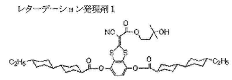

〔光学異方性層(C1)の形成/視認側偏光板の作製〕
下記化合物3-1~3-6を混合し、メチルエチルケトンに溶解して光学異方性層C1用塗布液を調製した。
――――――――――――――――――――――――――――――――――
光学異方性層C1用塗布液の組成
――――――――――――――――――――――――――――――――――
・ディスコティック液晶性化合物3-1 91.0質量部
・化合物3-2 9.0質量部
・重合開始剤:化合物3-3 3.0質量部
・重合開始剤:化合物3-4 1.0質量部
・含フッ素界面活性剤:化合物3-5 0.8質量部
・密着向上剤:化合物3-6 0.5質量部
・メチルエチルケトン 408質量部
――――――――――――――――――――――――――――――――――


下記化合物3-1~3-6を混合し、メチルエチルケトンに溶解して光学異方性層C1用塗布液を調製した。
――――――――――――――――――――――――――――――――――
光学異方性層C1用塗布液の組成
――――――――――――――――――――――――――――――――――
・ディスコティック液晶性化合物3-1 91.0質量部
・化合物3-2 9.0質量部
・重合開始剤:化合物3-3 3.0質量部
・重合開始剤:化合物3-4 1.0質量部
・含フッ素界面活性剤:化合物3-5 0.8質量部
・密着向上剤:化合物3-6 0.5質量部
・メチルエチルケトン 408質量部
――――――――――――――――――――――――――――――――――
塗布液を上記作製した光学異方性層(B1)に、#2.0のワイヤーバーを用いて塗布し、乾燥した。70℃で60秒加熱して、ディスコティック液晶性化合物を配向させた。
その後、ただちに70℃の温度条件で、290mJ/cm2の紫外線を照射して、ディスコティック液晶性化合物を重合させ、配向状態を固定し、光学異方性層(C1)を形成した。形成した光学異方性層(C1)の厚みは1μmであった。光学異方性層の厚みはレーザー膜厚計にて計測した。
なお、光学異方性層(C1)をガラス基板上に実施例と同条件で形成させ、光学異方性層のみのレターデーションを測定したところ、Re(550)=0nm、Rth(550)=40nm、波長分散を示すRe(450)/Re(550)=1.15であった。屈折率はnx=1.58とした。
その後、ただちに70℃の温度条件で、290mJ/cm2の紫外線を照射して、ディスコティック液晶性化合物を重合させ、配向状態を固定し、光学異方性層(C1)を形成した。形成した光学異方性層(C1)の厚みは1μmであった。光学異方性層の厚みはレーザー膜厚計にて計測した。
なお、光学異方性層(C1)をガラス基板上に実施例と同条件で形成させ、光学異方性層のみのレターデーションを測定したところ、Re(550)=0nm、Rth(550)=40nm、波長分散を示すRe(450)/Re(550)=1.15であった。屈折率はnx=1.58とした。
光学異方性層(B1)上に光学異方性層(C1)を形成させた後、保護膜と同様の方法で、片面保護膜付き偏光板01の保護膜と反対側に貼り合わせることにより、視認側偏光板を作製した。
〔バックライト側偏光板〕
視認側偏光板と同様の方法で、バックライト側偏光板を作製した。
視認側偏光板と同様の方法で、バックライト側偏光板を作製した。
〔液晶表示装置の作製〕
市販の垂直配向モード液晶表示装置(UN40EH6030F、Samsung社製)の表裏の偏光板を剥がして、上記作製した視認側偏光板およびバックライト側偏光板を互いの偏光子の吸収軸が直交するように貼り合わせることにより、実施例1-1の液晶表示装置を作製した。
市販の垂直配向モード液晶表示装置(UN40EH6030F、Samsung社製)の表裏の偏光板を剥がして、上記作製した視認側偏光板およびバックライト側偏光板を互いの偏光子の吸収軸が直交するように貼り合わせることにより、実施例1-1の液晶表示装置を作製した。
〔液晶表示装置の評価〕
作製した液晶表示装置を下記の方法で評価し、その結果を下記表2に記載した。
<表示性能(光漏れ、色変化)>
{光漏れの評価基準}
暗室内で液晶表示装置の黒表示時に測定機(EZ-Contrast XL88、ELDIM社製)を用いて黒輝度を計測した。極角60°における方位角45°、135°、225°、315°における輝度の平均値を光漏れYとして評価した。なお、偏光子の吸収軸は特に断りのない限り、視認側を方位角0°、バックライト側を方位角90°に配置している。
A: Y < 0.6(cd/m2)
B:0.6(cd/m2)≦ Y < 0.8(cd/m2)
C:0.8(cd/m2)≦ Y
作製した液晶表示装置を下記の方法で評価し、その結果を下記表2に記載した。
<表示性能(光漏れ、色変化)>
{光漏れの評価基準}
暗室内で液晶表示装置の黒表示時に測定機(EZ-Contrast XL88、ELDIM社製)を用いて黒輝度を計測した。極角60°における方位角45°、135°、225°、315°における輝度の平均値を光漏れYとして評価した。なお、偏光子の吸収軸は特に断りのない限り、視認側を方位角0°、バックライト側を方位角90°に配置している。
A: Y < 0.6(cd/m2)
B:0.6(cd/m2)≦ Y < 0.8(cd/m2)
C:0.8(cd/m2)≦ Y
{色変化の評価基準}
暗室内で液晶表示装置の黒表示時に測定機(EZ-Contrast XL88、ELDIM社製)を用いて色度を計測した。具体的には極角60°における方位角0°から345°まで15°刻みで色度u’、v’を算出し、各々u’、v’の最小値(u’min、v’min)、最大値(u’max、v’max)を抜き出し、以下の式で色変化Δu’v’を評価した。
Δu’v’=√((u’max - u’min)2+(v’max - v’min)2)
A:Δu’v’ < 0.1
B:0.1 ≦ Δu’v’ < 0.14
C:0.14 ≦ Δu’v’
暗室内で液晶表示装置の黒表示時に測定機(EZ-Contrast XL88、ELDIM社製)を用いて色度を計測した。具体的には極角60°における方位角0°から345°まで15°刻みで色度u’、v’を算出し、各々u’、v’の最小値(u’min、v’min)、最大値(u’max、v’max)を抜き出し、以下の式で色変化Δu’v’を評価した。
Δu’v’=√((u’max - u’min)2+(v’max - v’min)2)
A:Δu’v’ < 0.1
B:0.1 ≦ Δu’v’ < 0.14
C:0.14 ≦ Δu’v’
<耐久性(表示ムラ)>
作製した液晶表示装置について、40℃相対湿度95%で24時間サーモ後、25℃相対湿度60%で液晶表示装置のバックライトを点灯し、点灯から5~10時間後のパネルについて、その四隅の光漏れを、輝度計測用カメラ「ProMetric」(Radiant Imaging社製)で画面正面から黒表示画面を撮影し、全画面の平均輝度と、4角の光漏れが大きい箇所の輝度差をもとにして、評価した。
{表示ムラの評価基準}
A:パネル4角の光漏れが視認されない。(パネルの光漏れがサーモ投入前と同程度)
B:パネル4角のうち、1~2角でわずかな光漏れが視認されるが許容できる。
C:パネル4角のうち、3~4角でわずかな光漏れが視認されるが許容できる。
D:パネル4角の光漏れが強く、許容できない。
また25℃相対湿度60%で液晶表示装置のバックライトを5時間点灯の変わりに、40℃DRY環境で2時間サーモ後、25℃相対湿度60%で液晶表示装置のバックライトを24時間点灯として同様の評価を実施したが、光漏れ量や表示ムラの評価結果は25℃相対湿度60%で2時間放置の場合と同様であった。
作製した液晶表示装置について、40℃相対湿度95%で24時間サーモ後、25℃相対湿度60%で液晶表示装置のバックライトを点灯し、点灯から5~10時間後のパネルについて、その四隅の光漏れを、輝度計測用カメラ「ProMetric」(Radiant Imaging社製)で画面正面から黒表示画面を撮影し、全画面の平均輝度と、4角の光漏れが大きい箇所の輝度差をもとにして、評価した。
{表示ムラの評価基準}
A:パネル4角の光漏れが視認されない。(パネルの光漏れがサーモ投入前と同程度)
B:パネル4角のうち、1~2角でわずかな光漏れが視認されるが許容できる。
C:パネル4角のうち、3~4角でわずかな光漏れが視認されるが許容できる。
D:パネル4角の光漏れが強く、許容できない。
また25℃相対湿度60%で液晶表示装置のバックライトを5時間点灯の変わりに、40℃DRY環境で2時間サーモ後、25℃相対湿度60%で液晶表示装置のバックライトを24時間点灯として同様の評価を実施したが、光漏れ量や表示ムラの評価結果は25℃相対湿度60%で2時間放置の場合と同様であった。
<実施例1-2>
〔光学異方性層(B1)の形成〕
実施例1-1の光学異方性層(B1)の形成において、延伸温度を195℃に変更した以外は、実施例1-1と同様にして、下記表2に示す厚みおよび光学特性(Re、Rthおよび波長分散)を有する光学異方性層(B1)を形成した。
〔光学異方性層(B1)の形成〕
実施例1-1の光学異方性層(B1)の形成において、延伸温度を195℃に変更した以外は、実施例1-1と同様にして、下記表2に示す厚みおよび光学特性(Re、Rthおよび波長分散)を有する光学異方性層(B1)を形成した。
〔光学異方性層(C1)の形成/視認側偏光板の作製〕
上記光学異方性層(B1)を用いた以外は、実施例1-1と同様にして、下記表2に示す厚みおよび光学特性(Re、Rthおよび波長分散)を有する光学異方性層(C1)を形成し、視認側偏光板を作製した。
上記光学異方性層(B1)を用いた以外は、実施例1-1と同様にして、下記表2に示す厚みおよび光学特性(Re、Rthおよび波長分散)を有する光学異方性層(C1)を形成し、視認側偏光板を作製した。
〔バックライト側偏光板〕
視認側偏光板と同様の方法で、バックライト側偏光板を作製した。
視認側偏光板と同様の方法で、バックライト側偏光板を作製した。
〔液晶表示装置の作製、評価〕
上記で作製した偏光板を用いた以外は、実施例1-1と同様にして液晶表示装置を作製し、評価を行った。
上記で作製した偏光板を用いた以外は、実施例1-1と同様にして液晶表示装置を作製し、評価を行った。
<実施例1-3>
〔光学異方性層(B1)の形成〕
特開2009-063983号公報の実施例に記載のフィルム試料No.110およびフィルム試料No.111の作製方法を参考に、下記に示す組成、延伸方法、延伸温度および延伸倍率を変更し、下記表2に示す厚みおよび光学特性(Re、Rthおよび波長分散)を有する光学異方性層(B1)を作製した。
(セルロースアセテートの組成)
――――――――――――――――――――――――――――――――――
・セルロースアセテート(アセチル置換度2.86) 100質量部
・トリフェニルホスフェート 6.6質量部
・ビフェニルジフェニルホスフェート 4.7質量部
・レターデーション発現剤1 5.0質量部
――――――――――――――――――――――――――――――――――
(延伸方法) 固定端2軸延伸
(延伸温度) 180℃
(延伸倍率) 40%、TD方向
(延伸緩和) 45%、MD方向
〔光学異方性層(B1)の形成〕
特開2009-063983号公報の実施例に記載のフィルム試料No.110およびフィルム試料No.111の作製方法を参考に、下記に示す組成、延伸方法、延伸温度および延伸倍率を変更し、下記表2に示す厚みおよび光学特性(Re、Rthおよび波長分散)を有する光学異方性層(B1)を作製した。
(セルロースアセテートの組成)
――――――――――――――――――――――――――――――――――
・セルロースアセテート(アセチル置換度2.86) 100質量部
・トリフェニルホスフェート 6.6質量部
・ビフェニルジフェニルホスフェート 4.7質量部
・レターデーション発現剤1 5.0質量部
――――――――――――――――――――――――――――――――――
(延伸方法) 固定端2軸延伸
(延伸温度) 180℃
(延伸倍率) 40%、TD方向
(延伸緩和) 45%、MD方向
〔光学異方性層(C1)の形成/視認側偏光板の作製〕
実施例1-1の光学異方性層(C1)の形成において、メチルエチルケトンを237質量部に変更した以外は、実施例1-1と同様にして光学異方性層C1用塗布液を調製した。
次いで、上記光学異方性層(B1)および上記光学異方性層C1用塗布液を用いた以外は、実施例1-1と同様にして、下記表2に示す厚みおよび光学特性(Re、Rthおよび波長分散)を有する光学異方性層(C1)を形成し、視認側偏光板を作製した。
実施例1-1の光学異方性層(C1)の形成において、メチルエチルケトンを237質量部に変更した以外は、実施例1-1と同様にして光学異方性層C1用塗布液を調製した。
次いで、上記光学異方性層(B1)および上記光学異方性層C1用塗布液を用いた以外は、実施例1-1と同様にして、下記表2に示す厚みおよび光学特性(Re、Rthおよび波長分散)を有する光学異方性層(C1)を形成し、視認側偏光板を作製した。
〔バックライト側偏光板〕
視認側偏光板と同様の方法で、バックライト側偏光板を作製した。
視認側偏光板と同様の方法で、バックライト側偏光板を作製した。
〔液晶表示装置の作製、評価〕
上記で作製した偏光板を用いた以外は、実施例1-1と同様にして液晶表示装置を作製し、評価を行った。
上記で作製した偏光板を用いた以外は、実施例1-1と同様にして液晶表示装置を作製し、評価を行った。
<実施例1-4>
〔光学異方性層(B1)の形成〕
実施例1-1の光学異方性層(B1)の形成において、延伸倍率を10%に変更し、膜厚を70μmにした以外は、実施例1-1と同様にして、下記表2に示す厚みおよび光学特性(Re、Rthおよび波長分散)を有する光学異方性層(B1)を形成した。
〔光学異方性層(B1)の形成〕
実施例1-1の光学異方性層(B1)の形成において、延伸倍率を10%に変更し、膜厚を70μmにした以外は、実施例1-1と同様にして、下記表2に示す厚みおよび光学特性(Re、Rthおよび波長分散)を有する光学異方性層(B1)を形成した。
〔光学異方性層(C1)の形成/視認側偏光板の作製〕
上記光学異方性層(B1)を用いた以外は、実施例1-1と同様にして、下記表2に示す厚みおよび光学特性(Re、Rthおよび波長分散)を有する光学異方性層(C1)を形成し、視認側偏光板を作製した。
上記光学異方性層(B1)を用いた以外は、実施例1-1と同様にして、下記表2に示す厚みおよび光学特性(Re、Rthおよび波長分散)を有する光学異方性層(C1)を形成し、視認側偏光板を作製した。
〔バックライト側偏光板〕
視認側偏光板と同様の方法で、バックライト側偏光板を作製した。
視認側偏光板と同様の方法で、バックライト側偏光板を作製した。
〔液晶表示装置の作製、評価〕
上記で作製した偏光板を用いた以外は、実施例1-1と同様にして液晶表示装置を作製し、評価を行った。
上記で作製した偏光板を用いた以外は、実施例1-1と同様にして液晶表示装置を作製し、評価を行った。
<実施例1-5>
〔光学異方性層(B1)の形成〕
実施例1-3の光学異方性層(B1)の形成において、延伸倍率を35%に変更し、膜厚を89μmにした以外は、実施例1-1と同様にして、下記表2に示す厚みおよび光学特性(Re、Rthおよび波長分散)を有する光学異方性層(B1)を形成した。
〔光学異方性層(B1)の形成〕
実施例1-3の光学異方性層(B1)の形成において、延伸倍率を35%に変更し、膜厚を89μmにした以外は、実施例1-1と同様にして、下記表2に示す厚みおよび光学特性(Re、Rthおよび波長分散)を有する光学異方性層(B1)を形成した。
〔光学異方性層(C1)の形成/視認側偏光板の作製〕
上記光学異方性層(B1)を用いた以外は、実施例1-1と同様にして、下記表2に示す厚みおよび光学特性(Re、Rthおよび波長分散)を有する光学異方性層(C1)を形成し、視認側偏光板を作製した。
上記光学異方性層(B1)を用いた以外は、実施例1-1と同様にして、下記表2に示す厚みおよび光学特性(Re、Rthおよび波長分散)を有する光学異方性層(C1)を形成し、視認側偏光板を作製した。
〔バックライト側偏光板〕
視認側偏光板と同様の方法で、バックライト側偏光板を作製した。
視認側偏光板と同様の方法で、バックライト側偏光板を作製した。
〔液晶表示装置の作製、評価〕
上記で作製した偏光板を用いた以外は、実施例1-1と同様にして液晶表示装置を作製し、評価を行った。
上記で作製した偏光板を用いた以外は、実施例1-1と同様にして液晶表示装置を作製し、評価を行った。
<実施例1-6>
〔光学異方性層(B1)の形成〕
<合成例1>
(スピロ[フルオレン-9,8'-トリシクロ[4.3.0.12,5][3]デセン](endo体、下記式(A)参照)の合成)
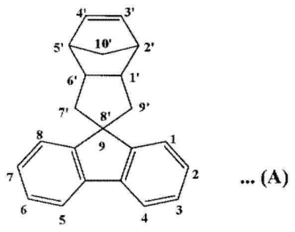
〔光学異方性層(B1)の形成〕
<合成例1>
(スピロ[フルオレン-9,8'-トリシクロ[4.3.0.12,5][3]デセン](endo体、下記式(A)参照)の合成)
滴下ロートを取り付けた1000mlフラスコにフルオレン15.52g(0.0934mol)をはかり取り、系内を窒素置換した。これに脱水THF 165mlを加え、スターラーにてよく攪拌して溶解させた。次にn-ブチルリチウムの1.6mol/lヘキサン溶液117mlを反応系の温度をドライアイスバス中で-78℃に保ちながら徐々に滴下した。滴下終了後、反応系を-78℃に保持しつつ、1時間攪拌を継続した。この反応液中に、下記式(B)で表される2endo,3endo-ビス-(トルエン-4-スルホニルオキシ)-5-ノルボルネン(endo体)21.60gを予め脱水THF 500mlに溶解させたものを、反応系の温度を-78℃に保ちながら徐々に滴下した。滴下終了後、ドライアイスバス中で1時間攪拌を継続し、その後、冷却バスを取りのぞき、反応系が完全に室温に戻るまで攪拌を継続した(約3時間)。これに、食塩水を添加してクエンチした後、反応液を蒸留水で3回洗浄を行い、硫酸ナトリウムを用いて乾燥させた。その後、減圧、加熱して溶媒を除去し、得られた結晶をメタノールを用いて再結晶させ、薄黄色の結晶として、上記式(A)で表されるスピロ[フルオレン-9,8'-トリシクロ[4.3.0.12,5][3]デセン](endo体)5.68gを得た。

<重合体合成例1>
ノルボルネン系単量体(Im)として、上記構造式(A)で表されるスピロ[フルオレン-9,8'-トリシクロ[4.3.0.12,5][3]デセン](endo体)1.90g、下記式(C)で表される8-メトキシカルボニル-8-メチルテトラシクロ[4.4.0.12,5.17,10]-3-ドデセン5.5g、分子量調節剤の1-ヘキセン 0.391g、および、トルエン 16.4gを、窒素置換した反応容器に仕込み、80℃に加熱した。これにトリエチルアルミニウム(0.6モル/L)のトルエン溶液0.169ml、メタノール変性WCl6のトルエン溶液(0.025モル/L)0.138mlを加え、80℃で3時間反応させることにより開環共重合体溶液を得た。得られた開環共重合体の重量平均分子量(Mw)は10.0×104であり、分子量分布(Mw/Mn)は4.80であった。
ノルボルネン系単量体(Im)として、上記構造式(A)で表されるスピロ[フルオレン-9,8'-トリシクロ[4.3.0.12,5][3]デセン](endo体)1.90g、下記式(C)で表される8-メトキシカルボニル-8-メチルテトラシクロ[4.4.0.12,5.17,10]-3-ドデセン5.5g、分子量調節剤の1-ヘキセン 0.391g、および、トルエン 16.4gを、窒素置換した反応容器に仕込み、80℃に加熱した。これにトリエチルアルミニウム(0.6モル/L)のトルエン溶液0.169ml、メタノール変性WCl6のトルエン溶液(0.025モル/L)0.138mlを加え、80℃で3時間反応させることにより開環共重合体溶液を得た。得られた開環共重合体の重量平均分子量(Mw)は10.0×104であり、分子量分布(Mw/Mn)は4.80であった。
次いで得られた開環共重合体溶液をオートクレーブに入れ、さらにトルエンを83.8g加えた。水添触媒であるRuHCl(CO)[P(C6H5)]3をモノマー仕込み量に対して2500ppm添加し、水素ガス圧を9~10MPaとし、160~165℃にて3時間の反応を行った。反応終了後、多量のメタノール溶液に沈殿させることにより水素添加物を得た。得られた開環共重合体の水素添加物(樹脂(P1))は、重量平均分子量(Mw)=9.15×10⁴、分子量分布(Mw/Mn)=3.76、固有粘度[η]=0.63、ガラス転移温度(Tg)=184.0℃であった。
また、樹脂(P1)におけるスピロ[フルオレン-9,8'-トリシクロ[4.3.0.12,5][3]デセン](endo体)に由来する構造単位(I)の割合が20.6モル%、8-メチル-8-メトキシカルボニルテトラシクロ〔4.4.0.12,5.17,10〕-3-ドデセンに由来する構造単位(II)の割合が79.4モル%であった。また、樹脂(P1)を1H-NMRにより分析した結果、オレフィン性二重結合に対する水素添加率は99%以上であり、また、芳香環の残存率は実質的に100%であった。

<光学異方性層(B1)の作製>
上記の合成例1で得た樹脂(P1)を塩化メチレンキャスト法により厚さ110μm、溶媒残留量0.2%以下の無色透明なキャストフィルムを得た。このフィルムをテンター内で、Tg+10℃である194℃に加熱し、延伸速度220%/分でTD方向に70%、MD方向に3%延伸した後、冷却して取り出し、下記表2に示す厚みおよび光学特性(Re、Rthおよび波長分散)を有する光学異方性層(B1)を得た。屈折率はnx=1.52として光学特性を測定した。
上記の合成例1で得た樹脂(P1)を塩化メチレンキャスト法により厚さ110μm、溶媒残留量0.2%以下の無色透明なキャストフィルムを得た。このフィルムをテンター内で、Tg+10℃である194℃に加熱し、延伸速度220%/分でTD方向に70%、MD方向に3%延伸した後、冷却して取り出し、下記表2に示す厚みおよび光学特性(Re、Rthおよび波長分散)を有する光学異方性層(B1)を得た。屈折率はnx=1.52として光学特性を測定した。
〔光学異方性層(C1)の形成/視認側偏光板の作製〕
上記光学異方性層(B1)を用いた以外は、実施例1-1と同様にして、下記表2に示す厚みおよび光学特性(Re、Rthおよび波長分散)を有する光学異方性層(C1)を形成し、視認側偏光板を作製した。
上記光学異方性層(B1)を用いた以外は、実施例1-1と同様にして、下記表2に示す厚みおよび光学特性(Re、Rthおよび波長分散)を有する光学異方性層(C1)を形成し、視認側偏光板を作製した。
〔バックライト側偏光板〕
視認側偏光板と同様の方法で、バックライト側偏光板を作製した。
視認側偏光板と同様の方法で、バックライト側偏光板を作製した。
〔液晶表示装置の作製、評価〕
上記で作製した偏光板を用いた以外は、実施例1-1と同様にして液晶表示装置を作製し、評価を行った。
上記で作製した偏光板を用いた以外は、実施例1-1と同様にして液晶表示装置を作製し、評価を行った。
<実施例1-7>
〔保護膜の作製〕
<延伸PET100μm>
以下に示すように、テレフタル酸及びエチレングリコールを直接反応させて水を留去し、エステル化した後、減圧下で重縮合を行なう直接エステル化法を用いて、連続重合装置により原料ポリエステル1(Sb触媒系PET)を得た。
〔保護膜の作製〕
<延伸PET100μm>
以下に示すように、テレフタル酸及びエチレングリコールを直接反応させて水を留去し、エステル化した後、減圧下で重縮合を行なう直接エステル化法を用いて、連続重合装置により原料ポリエステル1(Sb触媒系PET)を得た。
(1)エステル化反応
第一エステル化反応槽に、高純度テレフタル酸4.7トンとエチレングリコール1.8トンを90分かけて混合してスラリー形成させ、3800kg/hの流量で連続的に第一エステル化反応槽に供給した。更に三酸化アンチモンのエチレングリコール溶液を連続的に供給し、反応槽内温度250℃、攪拌下、平均滞留時間約4.3時間で反応を行なった。このとき、三酸化アンチモンはSb添加量が元素換算値で150ppmとなるように連続的に添加した。
第一エステル化反応槽に、高純度テレフタル酸4.7トンとエチレングリコール1.8トンを90分かけて混合してスラリー形成させ、3800kg/hの流量で連続的に第一エステル化反応槽に供給した。更に三酸化アンチモンのエチレングリコール溶液を連続的に供給し、反応槽内温度250℃、攪拌下、平均滞留時間約4.3時間で反応を行なった。このとき、三酸化アンチモンはSb添加量が元素換算値で150ppmとなるように連続的に添加した。
この反応物を第二エステル化反応槽に移送し、攪拌下、反応槽内温度250℃で、平均滞留時間で1.2時間反応させた。第二エステル化反応槽には、酢酸マグネシウムのエチレングリコール溶液と、リン酸トリメチルのエチレングリコール溶液を、Mg添加量およびP添加量が元素換算値でそれぞれ65ppm、35ppmになるように連続的に供給した。
(2)重縮合反応
上記で得られたエステル化反応生成物を連続的に第一重縮合反応槽に供給し、攪拌下、反応温度270℃、反応槽内圧力20torr(2.67×10⁻³MPa)で、平均滞留時間約1.8時間で重縮合させた。
上記で得られたエステル化反応生成物を連続的に第一重縮合反応槽に供給し、攪拌下、反応温度270℃、反応槽内圧力20torr(2.67×10⁻³MPa)で、平均滞留時間約1.8時間で重縮合させた。
更に、第二重縮合反応槽に移送し、この反応槽において攪拌下、反応槽内温度276℃、反応槽内圧力5torr(6.67×10⁻⁴MPa)で滞留時間約1.2時間の条件で反応(重縮合)させた。
次いで、更に第三重縮合反応槽に移送し、この反応槽では、反応槽内温度278℃、反応槽内圧力1.5torr(2.0×10⁻⁴MPa)で、滞留時間1.5時間の条件で反応(重縮合)させ、反応物(ポリエチレンテレフタレート(PET))を得た。
次に、得られた反応物を、冷水にストランド状に吐出し、直ちにカッティングしてポリエステルのペレット<断面:長径約4mm、短径約2mm、長さ:約3mm>を作製した。
得られたポリマーは、固有粘度IV=0.63であった。このポリマーを原料ポリエステル1とした。
固有粘度IVは、原料ポリエステル1を、1,1,2,2-テトラクロルエタン/フェノール(=2/3[質量比])混合溶媒に溶解し、該混合溶媒中の25℃での溶液粘度から求めた。
得られたポリマーは、固有粘度IV=0.63であった。このポリマーを原料ポリエステル1とした。
固有粘度IVは、原料ポリエステル1を、1,1,2,2-テトラクロルエタン/フェノール(=2/3[質量比])混合溶媒に溶解し、該混合溶媒中の25℃での溶液粘度から求めた。
(原料ポリエステル2)
乾燥させた紫外線吸収剤(2,2’-(1,4-フェニレン)ビス(4H-3,1-ベンズオキサジノン-4-オン)10質量部、原料ポリエステル1(IV=0.63)90質量部を混合し、混練押出機を用い、紫外線吸収剤を含有する原料ポリエステル2を得た。
乾燥させた紫外線吸収剤(2,2’-(1,4-フェニレン)ビス(4H-3,1-ベンズオキサジノン-4-オン)10質量部、原料ポリエステル1(IV=0.63)90質量部を混合し、混練押出機を用い、紫外線吸収剤を含有する原料ポリエステル2を得た。
(製造例)
<3層共押PET80μm>
-フィルム成形工程-
原料ポリエステル1(90質量部)と、紫外線吸収剤を含有した原料ポリエステル2(10質量部)を、含水率20ppm以下に乾燥させた後、直径50mmの1軸混練押出機1のホッパー1に投入し、押出機1で300℃に溶融した(中間層II層)。また原料ポリエステル1を、含水率20ppm以下に乾燥させた後、直径30mmの1軸混練押出機2のホッパー2に投入し、押出機2で300℃に溶融した(外層I層、外層III層)。
これらの2種のポリマー溶融物をそれぞれギアポンプ、濾過器(孔径20μm)に介した後、2種3層合流ブロックにて、押出機1から押出されたポリマーが中間層(II層)に、押出機2から押出されたポリマーが外層(I層及びIII層)になるように積層し、ダイよりシート状に押し出した。
溶融樹脂の押出条件は、圧力変動を1%、溶融樹脂の温度分布を2%として、溶融樹脂をダイから押出した。具体的には、背圧を、押出機のバレル内平均圧力に対して1%加圧し、押出機の配管温度を、押出機のバレル内平均温度に対して2%高い温度で加熱した。
ダイから押出した溶融樹脂は、温度25℃に設定された冷却キャストドラム上に押出し、静電印加法を用い冷却キャストドラムに密着させた。冷却キャストドラムに対向配置された剥ぎ取りロールを用いて剥離し、未延伸ポリエステルフィルム2を得た。このとき、I層、II層、III層の厚さの比は10:80:10となるように各押出機の吐出量を調整した。
<3層共押PET80μm>
-フィルム成形工程-
原料ポリエステル1(90質量部)と、紫外線吸収剤を含有した原料ポリエステル2(10質量部)を、含水率20ppm以下に乾燥させた後、直径50mmの1軸混練押出機1のホッパー1に投入し、押出機1で300℃に溶融した(中間層II層)。また原料ポリエステル1を、含水率20ppm以下に乾燥させた後、直径30mmの1軸混練押出機2のホッパー2に投入し、押出機2で300℃に溶融した(外層I層、外層III層)。
これらの2種のポリマー溶融物をそれぞれギアポンプ、濾過器(孔径20μm)に介した後、2種3層合流ブロックにて、押出機1から押出されたポリマーが中間層(II層)に、押出機2から押出されたポリマーが外層(I層及びIII層)になるように積層し、ダイよりシート状に押し出した。
溶融樹脂の押出条件は、圧力変動を1%、溶融樹脂の温度分布を2%として、溶融樹脂をダイから押出した。具体的には、背圧を、押出機のバレル内平均圧力に対して1%加圧し、押出機の配管温度を、押出機のバレル内平均温度に対して2%高い温度で加熱した。
ダイから押出した溶融樹脂は、温度25℃に設定された冷却キャストドラム上に押出し、静電印加法を用い冷却キャストドラムに密着させた。冷却キャストドラムに対向配置された剥ぎ取りロールを用いて剥離し、未延伸ポリエステルフィルム2を得た。このとき、I層、II層、III層の厚さの比は10:80:10となるように各押出機の吐出量を調整した。
得られた未延伸ポリエステルフィルム2を、下記条件で横延伸し、厚さ80μm、面内方向のレターデーションReが8200nm、膜厚方向のレターデーションRthが9400nmのPETフィルムを製造した。
{条件}
・横延伸温度:90℃
・横延伸倍率:4.3倍
{条件}
・横延伸温度:90℃
・横延伸倍率:4.3倍
(熱固定部)
次いで、ポリエステルフィルムの膜面温度を下記範囲に制御しながら、熱固定処理を行った。
{条件}
・熱固定温度:180℃
・熱固定時間:15秒
次いで、ポリエステルフィルムの膜面温度を下記範囲に制御しながら、熱固定処理を行った。
{条件}
・熱固定温度:180℃
・熱固定時間:15秒
(熱緩和部)
熱固定後のポリエステルフィルムを下記の温度に加熱し、フィルムを緩和した。
{条件}
・熱緩和温度:170℃
・熱緩和率:TD方向(フィルム幅方向、横方向)2%
熱固定後のポリエステルフィルムを下記の温度に加熱し、フィルムを緩和した。
{条件}
・熱緩和温度:170℃
・熱緩和率:TD方向(フィルム幅方向、横方向)2%
(冷却部)
次に、熱緩和後のポリエステルフィルムを50℃の冷却温度にて冷却した。
次に、熱緩和後のポリエステルフィルムを50℃の冷却温度にて冷却した。
〔保護膜と偏光子との貼り合わせ〕
上記の製造例で作製したポリエステルフィルムを保護膜として用い、以下の方法にしたがって偏光子と接着層を介して貼合した。
なお、作製したポリエステルフィルムの透湿度は10g/m2/24hであった。また、Re(550)=8200nm、Rth(550)=9400nmであった。屈折率はnx=1.48とした。
上記の製造例で作製したポリエステルフィルムを保護膜として用い、以下の方法にしたがって偏光子と接着層を介して貼合した。
なお、作製したポリエステルフィルムの透湿度は10g/m2/24hであった。また、Re(550)=8200nm、Rth(550)=9400nmであった。屈折率はnx=1.48とした。
(偏光子側易接着層の形成)
(1)共重合ポリエステル樹脂(A-1)の合成
――――――――――――――――――――――――――――――――――
・ジメチルテレフタレート 194.2質量部
・ジメチルイソフタレート 184.5質量部
・ジメチル-5-ナトリウムスルホイソフタレート 14.8質量部
・ジエチレングリコール 233.5質量部
・エチレングリコール 136.6質量部
・テトラ-n-ブチルチタネート 0.2質量部
――――――――――――――――――――――――――――――――――
上記化合物を仕込み、160℃から220℃の温度で4時間かけてエステル交換反応を行なった。次いで255℃まで昇温し、反応系を徐々に減圧した後、30Paの減圧下で1時間30分反応させ、共重合ポリエステル樹脂(A-1)を得た。
(1)共重合ポリエステル樹脂(A-1)の合成
――――――――――――――――――――――――――――――――――
・ジメチルテレフタレート 194.2質量部
・ジメチルイソフタレート 184.5質量部
・ジメチル-5-ナトリウムスルホイソフタレート 14.8質量部
・ジエチレングリコール 233.5質量部
・エチレングリコール 136.6質量部
・テトラ-n-ブチルチタネート 0.2質量部
――――――――――――――――――――――――――――――――――
上記化合物を仕込み、160℃から220℃の温度で4時間かけてエステル交換反応を行なった。次いで255℃まで昇温し、反応系を徐々に減圧した後、30Paの減圧下で1時間30分反応させ、共重合ポリエステル樹脂(A-1)を得た。
(2)ポリエステル水分散体(Aw-1)の作製
――――――――――――――――――――――――――――――――――
・共重合ポリエステル樹脂(A-1) 30質量部
・エチレングリコールn-ブチルエーテル 15質量部
――――――――――――――――――――――――――――――――――
上記化合物を入れ、110℃で加熱、攪拌し樹脂を溶解した。樹脂が完全に溶解した後、水55質量部をポリエステル溶液に攪拌しつつ徐々に添加した。添加後、液を攪拌しつつ室温まで冷却して、固形分30質量%の乳白色のポリエステル水分散体(Aw-1)を作製した。
――――――――――――――――――――――――――――――――――
・共重合ポリエステル樹脂(A-1) 30質量部
・エチレングリコールn-ブチルエーテル 15質量部
――――――――――――――――――――――――――――――――――
上記化合物を入れ、110℃で加熱、攪拌し樹脂を溶解した。樹脂が完全に溶解した後、水55質量部をポリエステル溶液に攪拌しつつ徐々に添加した。添加後、液を攪拌しつつ室温まで冷却して、固形分30質量%の乳白色のポリエステル水分散体(Aw-1)を作製した。
(3)ポリビニルアルコール水溶液(Bw-1)の作製
水90質量部を入れ、攪拌しながらケン化度が88%で重合度500のポリビニルアルコール樹脂(クラレ製)(B-1)10質量部を徐々に添加した。添加後、液を攪拌しながら、95℃まで加熱し、樹脂を溶解させた。溶解後、攪拌しながら室温まで冷却して、固形分10質量%のポリビニルアルコール水溶液(Bw-1)を作製した。
水90質量部を入れ、攪拌しながらケン化度が88%で重合度500のポリビニルアルコール樹脂(クラレ製)(B-1)10質量部を徐々に添加した。添加後、液を攪拌しながら、95℃まで加熱し、樹脂を溶解させた。溶解後、攪拌しながら室温まで冷却して、固形分10質量%のポリビニルアルコール水溶液(Bw-1)を作製した。
(4)ブロックポリイソシアネート水分散液(C-1)の作製
――――――――――――――――――――――――――――――――――
・ヘキサメチレンジイソシアネートを原料とした
イソシアヌレート構造を有するポリイソシアネート化合物
(旭化成ケミカルズ製、デュラネートTPA) 100質量部
・プロピレングリコールモノメチルエーテルアセテート 55質量部
・ポリエチレングリコールモノメチルエーテル
(平均分子量750) 30質量部
――――――――――――――――――――――――――――――――――
上記化合物を仕込み、窒素雰囲気下、70℃で4時間保持した。その後、反応液温度を50℃に下げ、メチルエチルケトオキシム47質量部を滴下した。反応液の赤外スペクトルを測定し、イソシアネート基の吸収が消失したことを確認し、固形分75質量%のブロックポリイソシアネート水分散液(C-1)を得た。
――――――――――――――――――――――――――――――――――
・ヘキサメチレンジイソシアネートを原料とした
イソシアヌレート構造を有するポリイソシアネート化合物
(旭化成ケミカルズ製、デュラネートTPA) 100質量部
・プロピレングリコールモノメチルエーテルアセテート 55質量部
・ポリエチレングリコールモノメチルエーテル
(平均分子量750) 30質量部
――――――――――――――――――――――――――――――――――
上記化合物を仕込み、窒素雰囲気下、70℃で4時間保持した。その後、反応液温度を50℃に下げ、メチルエチルケトオキシム47質量部を滴下した。反応液の赤外スペクトルを測定し、イソシアネート基の吸収が消失したことを確認し、固形分75質量%のブロックポリイソシアネート水分散液(C-1)を得た。
下記の塗剤を混合し、ポリエステル系樹脂(A)/ポリビニルアルコール系樹脂(B)の質量比が70/30になる偏光子側易接着用の塗布液P1を作製した。
――――――――――――――――――――――――――――――――――
・水 40.61質量%
・イソプロパノール 30.00質量%
・ポリエステル水分散体(Aw-1) 11.67質量%
・ポリビニルアルコール水溶液(Bw-1) 15.00質量%
・ブロックイソシアネート系架橋剤(C-1) 0.67質量%
・粒子(平均粒径100nmのシリカゾル、固形分濃度40質量%)
1.25質量%
・触媒(有機スズ系化合物 固形分濃度14質量%) 0.3質量%
・界面活性剤(シリコン系、固形分濃度10質量%) 0.5質量%
――――――――――――――――――――――――――――――――――
――――――――――――――――――――――――――――――――――
・水 40.61質量%
・イソプロパノール 30.00質量%
・ポリエステル水分散体(Aw-1) 11.67質量%
・ポリビニルアルコール水溶液(Bw-1) 15.00質量%
・ブロックイソシアネート系架橋剤(C-1) 0.67質量%
・粒子(平均粒径100nmのシリカゾル、固形分濃度40質量%)
1.25質量%
・触媒(有機スズ系化合物 固形分濃度14質量%) 0.3質量%
・界面活性剤(シリコン系、固形分濃度10質量%) 0.5質量%
――――――――――――――――――――――――――――――――――
(ポリエステルフィルムへの易接着層の塗布)
リバースロール法にて、上記ポリエステルフィルム(保護膜)の片側に偏光子側易接着用の塗布液P1を乾燥後の塗布量が0.12g/m2になるように調整しながら、塗布した。
リバースロール法にて、上記ポリエステルフィルム(保護膜)の片側に偏光子側易接着用の塗布液P1を乾燥後の塗布量が0.12g/m2になるように調整しながら、塗布した。
ポリエステルフィルム試料の偏光子側易接着層用の塗布液P1が塗布された面を偏光子側としロールツーロールで積層し、得られた積層体に対して接着剤を硬化させるためにロール上を搬送しながら、70℃、相対湿度60%で加熱し、貼合した。このようにして、片面保護膜付き偏光板02を作製した。
〔液晶表示装置の作製、評価〕
上記で作製した片面保護膜付き偏光板02を用いた以外は、実施例1-1と同様にして液晶表示装置を作製し、評価を行った。
上記で作製した片面保護膜付き偏光板02を用いた以外は、実施例1-1と同様にして液晶表示装置を作製し、評価を行った。
<実施例1-8>
〔保護膜の作製〕
<熱可塑性樹脂フィルム1>
〔保護膜の作製〕
<熱可塑性樹脂フィルム1>

[上記一般式(1)中、R1は水素原子、R2およびR3はメチル基であるラクトン環構造を有する(メタ)アクリル系樹脂{共重合モノマー質量比=メタクリル酸メチル/2-(ヒドロキシメチル)アクリル酸メチル=8/2、ラクトン環化率約100%、ラクトン環構造の含有割合19.4%、質量平均分子量133000、メルトフローレート6.5g/10分(240℃、10kgf)、Tg131℃}90質量部と、アクリロニトリル-スチレン(AS)樹脂{トーヨーAS AS20、東洋スチレン社製}10質量部との混合物;Tg127℃]のペレットを二軸押し出し機に供給し、約280℃でシート状に溶融押し出しして、ラクトン環構造を有する(メタ)アクリル系樹脂シートを得た。この未延伸シートを、160℃の温度条件下、縦、横に延伸して熱可塑性樹脂フィルム(厚さ:40μm、面内位相差Re:0.8nm、厚み方向位相差Rth:1.5nm)を得た。
偏光子の片方の面に、アクリル接着剤を用いて、作製した熱可塑性樹脂フィルムにコロナ処理を施したのち、貼合して片面保護膜付き偏光板03を作製した。
〔液晶表示装置の作製、評価〕
上記で作製した片面保護膜付き偏光板03を用いた以外は、実施例1-1と同様にして液晶表示装置を作製し、評価を行った。
上記で作製した片面保護膜付き偏光板03を用いた以外は、実施例1-1と同様にして液晶表示装置を作製し、評価を行った。
<実施例1-9>
〔保護膜の作製〕
特開2011‐138119号公報の[0173]~[0176]に記載の方法で、イミド化樹脂を得た。
得られたイミド化樹脂(III)100重量部と、下記トリアジン化合物A0.10質量部を単軸押出機を用いてペレットにした。
上記ペレットを用いて、未延伸フィルムを縦方向、横方向に延伸して、その他条件は実施例1-8と同様の方法で熱可塑性樹脂フィルムを作製した。
〔保護膜の作製〕
特開2011‐138119号公報の[0173]~[0176]に記載の方法で、イミド化樹脂を得た。
得られたイミド化樹脂(III)100重量部と、下記トリアジン化合物A0.10質量部を単軸押出機を用いてペレットにした。
上記ペレットを用いて、未延伸フィルムを縦方向、横方向に延伸して、その他条件は実施例1-8と同様の方法で熱可塑性樹脂フィルムを作製した。

得られたフィルムの厚さは40μmであった。Re=1.0nmであり、Rth=3.0nmであった。
偏光子の片方の面に、アクリル接着剤を用いて、作製した熱可塑性樹脂フィルムをコロナ処理を施したのち、貼合して片面保護膜付き偏光板04を作製した。
〔液晶表示装置の作製、評価〕
上記で作製した片面保護膜付き偏光板04を用いた以外は実施例1-1と同様にして液晶表示装置を作製し、評価を行った
上記で作製した片面保護膜付き偏光板04を用いた以外は実施例1-1と同様にして液晶表示装置を作製し、評価を行った
<実施例1-10>
〔保護膜の作製〕
(組成物B-1の組成)
――――――――――――――――――――――――――――――――――
・A-DCP(100%):
トリシクロデカンジメタノールジメタクリレート
[新中村化学工業(株)製] 97.0質量部
・イルガキュア907(100%):重合開始剤
[チバ・スペシャルティ・ケミカルズ(株)製] 3.0質量部
・SP-13(レベリング剤): 0.04質量部
・MEK(メチルエチルケトン): 81.8質量部
――――――――――――――――――――――――――――――――――
〔保護膜の作製〕
(組成物B-1の組成)
――――――――――――――――――――――――――――――――――
・A-DCP(100%):
トリシクロデカンジメタノールジメタクリレート
[新中村化学工業(株)製] 97.0質量部
・イルガキュア907(100%):重合開始剤
[チバ・スペシャルティ・ケミカルズ(株)製] 3.0質量部
・SP-13(レベリング剤): 0.04質量部
・MEK(メチルエチルケトン): 81.8質量部
――――――――――――――――――――――――――――――――――

(基材フィルムの作製)
下記に記載の組成物をミキシングタンクに投入し、加熱しながら攪拌して、各成分を溶解し、ドープを調製した。
下記に記載の組成物をミキシングタンクに投入し、加熱しながら攪拌して、各成分を溶解し、ドープを調製した。
{セルロースエステル}
アシル基総置換度2.75、アセチル置換度0.19、プロピオニル置換度2.56、重量平均分子量200000のセルロースエステルを使用した。
このセルロースエステルは、以下のように合成した。
セルロースに触媒として硫酸(セルロース100質量部に対し7.8質量部)を添加し、アシル置換基の原料となるカルボン酸を添加して40℃でアシル化反応を行った。この時、カルボン酸の量を調整することでアセチル基及びプロピオニル基の置換度を調整した。またアシル化後に40℃で熟成を行った。更にこのセルロースエステルの低分子量成分をアセトンで洗浄し除去した。
アシル基総置換度2.75、アセチル置換度0.19、プロピオニル置換度2.56、重量平均分子量200000のセルロースエステルを使用した。
このセルロースエステルは、以下のように合成した。
セルロースに触媒として硫酸(セルロース100質量部に対し7.8質量部)を添加し、アシル置換基の原料となるカルボン酸を添加して40℃でアシル化反応を行った。この時、カルボン酸の量を調整することでアセチル基及びプロピオニル基の置換度を調整した。またアシル化後に40℃で熟成を行った。更にこのセルロースエステルの低分子量成分をアセトンで洗浄し除去した。
(ドープの組成)
――――――――――――――――――――――――――――――――――
・セルロースエステル 30.0質量部
・アクリル樹脂 70.0質量部
(ダイヤナールBR85 三菱レイヨン(株)製)
・チヌビン328 チバ・ジャパン製 1.0質量部
・メチレンクロライド 320質量部
・エタノール 45質量部
――――――――――――――――――――――――――――――――――
――――――――――――――――――――――――――――――――――
・セルロースエステル 30.0質量部
・アクリル樹脂 70.0質量部
(ダイヤナールBR85 三菱レイヨン(株)製)
・チヌビン328 チバ・ジャパン製 1.0質量部
・メチレンクロライド 320質量部
・エタノール 45質量部
――――――――――――――――――――――――――――――――――
バンド流延装置を用い、上記調製したドープをステンレス製のエンドレスバンド(流延支持体)に流延ダイから均一に流延した。ドープ中の残留溶媒量が40質量%になった時点で流延支持体から高分子膜として剥離し、テンターにて積極的に延伸をせずに搬送し、乾燥ゾーンで130℃で乾燥を行った。
得られたフィルムの厚さは40μmであった。また、得られた基材フィルムのReおよびRthの値を方法で測定したところ、Re=1.0nmであり、Rth=5.0nmであった。このフィルムを基材フィルムとした。
得られたフィルムの厚さは40μmであった。また、得られた基材フィルムのReおよびRthの値を方法で測定したところ、Re=1.0nmであり、Rth=5.0nmであった。このフィルムを基材フィルムとした。
上記基材フィルムに上記組成物B-1を使用し、特開2006-122889号公報実施例1に記載のスロットダイを用いたダイコート法で、搬送速度30m/分の条件で塗布し、60℃で150秒乾燥させた。その後、更に窒素パージ下酸素濃度約0.1%で160W/cmの空冷メタルハライドランプ(アイグラフィックス(株)製)を用いて、照度400mW/cm2、照射量60mJ/cm2の紫外線を照射して塗布層を硬化させ、巻き取った。塗布層の膜厚は12μmになるよう塗布量を調整した。得られた光学フィルムを保護膜Aとした。
<偏光板の作製>
偏光子の片方の面に、アクリル接着剤を用いて、作製した保護膜Aをコロナ処理を施したのち、貼合して片面保護膜付き偏光板05を作製した。
偏光子の片方の面に、アクリル接着剤を用いて、作製した保護膜Aをコロナ処理を施したのち、貼合して片面保護膜付き偏光板05を作製した。
〔液晶表示装置の作製、評価〕
上記で作製した片面保護膜付き偏光板05を用いた以外は、実施例1-1と同様にして液晶表示装置を作製し、評価を行った
上記で作製した片面保護膜付き偏光板05を用いた以外は、実施例1-1と同様にして液晶表示装置を作製し、評価を行った
<比較例1>
(ドープ調製)
下記に記載の組成物をミキシングタンクに投入し、加熱しながら攪拌して、各成分を溶解し、ドープを調製した。
下記に記載の組成物をミキシングタンクに投入し、加熱しながら攪拌して、各成分を溶解し、ドープを調製した。
[光学異方性層]
(ドープ組成)
――――――――――――――――――――――――――――――――――
・セルロースエステル(アセチル置換度2.81) 100質量部
・トリフェニルホスフェート 6.8質量部
・ビフェニルジフェニルホスフェート 4.9質量部
・レターデーション発現剤R-1 4.0質量部
・平均粒径16nmのシリカ粒子
(aerosil R972日本アエロジル(株)製) 0.15質量部
・ジクロロメタン 429.7質量部
・メタノール 64.2質量部
――――――――――――――――――――――――――――――――――
(ドープ組成)
――――――――――――――――――――――――――――――――――
・セルロースエステル(アセチル置換度2.81) 100質量部
・トリフェニルホスフェート 6.8質量部
・ビフェニルジフェニルホスフェート 4.9質量部
・レターデーション発現剤R-1 4.0質量部
・平均粒径16nmのシリカ粒子
(aerosil R972日本アエロジル(株)製) 0.15質量部
・ジクロロメタン 429.7質量部
・メタノール 64.2質量部
――――――――――――――――――――――――――――――――――
(レターデーション発現剤)
下記に記載のレターデーション発現剤を使用した。これらのレターデーション発現剤は公知の合成方法により入手可能である。
下記に記載のレターデーション発現剤を使用した。これらのレターデーション発現剤は公知の合成方法により入手可能である。
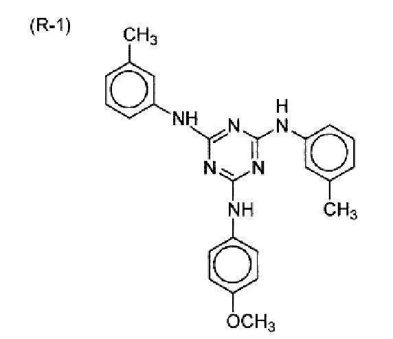
ドープの固形分濃度(セルロースエステル、アクリル樹脂、レターデーション発現剤の合計濃度)は19質量%であった。
バンド流延装置を用い、前記調製したドープを2000mm幅でステンレス製のエンドレスバンド(流延支持体)に流延ダイから均一に流延した。ドープ中の残留溶媒量が40質量%になった時点で流延支持体から高分子膜として剥離し、テンターにて積極的に延伸をせずに搬送し、乾燥ゾーンで130℃で乾燥を行った後、得られた未延伸フィルムの膜厚は70μm、ガラス転移温度Tgは142℃であった。
また、上記と同様の方法で流延を行い、支持体から剥離した高分子膜の両端をクリップを有したテンターで固定して、幅方向(TD方向)に延伸し、搬送ながら乾燥ゾーンで130℃で乾燥し、耳部をスリットして幅1500mmのフィルムを得た。テンターで延伸を始めたときの高分子膜中の残留溶剤量は10質量%であった。ここで、搬送方向(MD方向)については、ステンレスバンドと支持体の回転速度とテンターの運動速度から算出すると、搬送により若干延伸された。延伸時の温度は140℃、MD方向の延伸倍率を1.02、TD方向の延伸倍率を1.30になるようにした。
作製した光学異方性層の厚みおよび光学特性(Re、Rthおよび波長分散)を下記表2に示す。
また、上記と同様の方法で流延を行い、支持体から剥離した高分子膜の両端をクリップを有したテンターで固定して、幅方向(TD方向)に延伸し、搬送ながら乾燥ゾーンで130℃で乾燥し、耳部をスリットして幅1500mmのフィルムを得た。テンターで延伸を始めたときの高分子膜中の残留溶剤量は10質量%であった。ここで、搬送方向(MD方向)については、ステンレスバンドと支持体の回転速度とテンターの運動速度から算出すると、搬送により若干延伸された。延伸時の温度は140℃、MD方向の延伸倍率を1.02、TD方向の延伸倍率を1.30になるようにした。
作製した光学異方性層の厚みおよび光学特性(Re、Rthおよび波長分散)を下記表2に示す。
〔視認側偏光板の作製〕
上記光学異方性層(B1)を用い、光学異方性層(C1)を形成しなかった以外は、実施例1-1と同様にして、視認側偏光板を作製した。
上記光学異方性層(B1)を用い、光学異方性層(C1)を形成しなかった以外は、実施例1-1と同様にして、視認側偏光板を作製した。
〔バックライト側偏光板〕
視認側偏光板と同様の方法で、バックライト側偏光板を作製した。
視認側偏光板と同様の方法で、バックライト側偏光板を作製した。
〔液晶表示装置の作製、評価〕
上記で作製した偏光板を用いた以外は、実施例1-1と同様にして液晶表示装置を作製し、評価を行った。
上記で作製した偏光板を用いた以外は、実施例1-1と同様にして液晶表示装置を作製し、評価を行った。
<比較例2>
〔光学異方性層(B1)の形成〕
実施例1-1の光学異方性層(B1)の形成において、延伸温度を195℃に変更し、延伸倍率を10%に変更した以外は、実施例1-1と同様にして、下記表2に示す厚みおよび光学特性(Re、Rthおよび波長分散)を有する光学異方性層を形成した。
実施例1-1の光学異方性層(B1)の形成において、延伸温度を195℃に変更し、延伸倍率を10%に変更した以外は、実施例1-1と同様にして、下記表2に示す厚みおよび光学特性(Re、Rthおよび波長分散)を有する光学異方性層を形成した。
〔光学異方性層(C1)の形成/視認側偏光板の作製〕
上記光学異方性層(B1)を用いた以外は、実施例1-1と同様にして、下記表2に示す厚みおよび光学特性(Re、Rthおよび波長分散)を有する光学異方性層(C1)を形成し、視認側偏光板を作製した。
上記光学異方性層(B1)を用いた以外は、実施例1-1と同様にして、下記表2に示す厚みおよび光学特性(Re、Rthおよび波長分散)を有する光学異方性層(C1)を形成し、視認側偏光板を作製した。
〔バックライト側偏光板〕
視認側偏光板と同様の方法で、バックライト側偏光板を作製した。
視認側偏光板と同様の方法で、バックライト側偏光板を作製した。
〔液晶表示装置の作製、評価〕
上記で作製した偏光板を用いた以外は、実施例1-1と同様にして液晶表示装置を作製し、評価を行った。
上記で作製した偏光板を用いた以外は、実施例1-1と同様にして液晶表示装置を作製し、評価を行った。
<比較例3>
〔光学異方性層(B1)の形成〕
実施例1-3の光学異方性層B1の形成において、延伸倍率を35%に変更した以外は、実施例1-1と同様にして、下記表2に示す厚みおよび光学特性(Re、Rthおよび波長分散)を有する光学異方性層を形成した。
〔光学異方性層(B1)の形成〕
実施例1-3の光学異方性層B1の形成において、延伸倍率を35%に変更した以外は、実施例1-1と同様にして、下記表2に示す厚みおよび光学特性(Re、Rthおよび波長分散)を有する光学異方性層を形成した。
〔光学異方性層(C1)の形成/視認側偏光板の作製〕
上記光学異方性層(B1)を用いた以外は、実施例1-3と同様にして、下記表2に示す厚みおよび光学特性(Re、Rthおよび波長分散)を有する光学異方性層(C1)を形成し、視認側偏光板を作製した。
上記光学異方性層(B1)を用いた以外は、実施例1-3と同様にして、下記表2に示す厚みおよび光学特性(Re、Rthおよび波長分散)を有する光学異方性層(C1)を形成し、視認側偏光板を作製した。
〔バックライト側偏光板〕
視認側偏光板と同様の方法で、バックライト側偏光板を作製した。
視認側偏光板と同様の方法で、バックライト側偏光板を作製した。
〔液晶表示装置の作製、評価〕
上記で作製した偏光板を用いた以外は、実施例1-3と同様にして液晶表示装置を作製し、評価を行った。
上記で作製した偏光板を用いた以外は、実施例1-3と同様にして液晶表示装置を作製し、評価を行った。
[第2の態様]
<実施例2-1>
実施例1-1と同様の方法により、片面保護膜付き偏光板01を作製した。
<実施例2-1>
実施例1-1と同様の方法により、片面保護膜付き偏光板01を作製した。
〔光学異方性層(C1)の形成〕
次いで、実施例1-1で調製した光学異方性層(C1)の塗布液においてメチルエチルケトンを152質量部に変更し、上記作製した片面保護膜付き偏光板01の偏光子側の面に、#2.0のワイヤーバーを用いて塗布し、乾燥した。70℃で60秒加熱して、ディスコティック液晶性化合物を配向させた。
その後、ただちに70℃の温度条件で、290mJ/cm2の紫外線を照射して、ディスコティック液晶性化合物を重合させ、配向状態を固定し、光学異方性層(C1)を形成した。形成した光学異方性層(C1)の厚みは1μmであった。光学異方性層の厚みはレーザー膜厚計にて計測した。
なお、光学異方性層(C1)をガラス基板上に実施例と同条件で形成させ、光学異方性層のみのレターデーションを測定したところ、Re(550)=0nm、Rth(550)=80nm、波長分散を示すRe(450)/Re(550)=1.15であった。屈折率はnx=1.58とした。
次いで、実施例1-1で調製した光学異方性層(C1)の塗布液においてメチルエチルケトンを152質量部に変更し、上記作製した片面保護膜付き偏光板01の偏光子側の面に、#2.0のワイヤーバーを用いて塗布し、乾燥した。70℃で60秒加熱して、ディスコティック液晶性化合物を配向させた。
その後、ただちに70℃の温度条件で、290mJ/cm2の紫外線を照射して、ディスコティック液晶性化合物を重合させ、配向状態を固定し、光学異方性層(C1)を形成した。形成した光学異方性層(C1)の厚みは1μmであった。光学異方性層の厚みはレーザー膜厚計にて計測した。
なお、光学異方性層(C1)をガラス基板上に実施例と同条件で形成させ、光学異方性層のみのレターデーションを測定したところ、Re(550)=0nm、Rth(550)=80nm、波長分散を示すRe(450)/Re(550)=1.15であった。屈折率はnx=1.58とした。
〔光学異方性層(B1)の形成〕
実施例1-1の光学異方性層B1の形成において、延伸温度を195℃に変更し、膜厚を26μmにした以外は、実施例1-1と同様にして、下記表3に示す光学特性(Re、Rthおよび波長分散)を有する光学異方性層を形成した。
実施例1-1の光学異方性層B1の形成において、延伸温度を195℃に変更し、膜厚を26μmにした以外は、実施例1-1と同様にして、下記表3に示す光学特性(Re、Rthおよび波長分散)を有する光学異方性層を形成した。
〔視認側偏光板の作製〕
上記光学異方性層(B1)と、上記光学異方性層(C1)を形成した片面保護膜付き偏光板01の光学異方性層(C1)側とを、PVA((株)クラレ製、PVA-117H)3%水溶液を接着剤として用いて貼りあわせて視認側偏光板を作製した。
上記光学異方性層(B1)と、上記光学異方性層(C1)を形成した片面保護膜付き偏光板01の光学異方性層(C1)側とを、PVA((株)クラレ製、PVA-117H)3%水溶液を接着剤として用いて貼りあわせて視認側偏光板を作製した。
〔バックライト側偏光板〕
視認側偏光板と同様の方法で、バックライト側偏光板を作製した。
視認側偏光板と同様の方法で、バックライト側偏光板を作製した。
〔液晶表示装置の作製および評価〕
実施例1-1と同様の方法により、実施例2-1の液晶表示装置を作製した。
作製した液晶表示装置について、実施例1-1と同様の方法により評価した。その結果を表3に記載した。
実施例1-1と同様の方法により、実施例2-1の液晶表示装置を作製した。
作製した液晶表示装置について、実施例1-1と同様の方法により評価した。その結果を表3に記載した。
<実施例2-2>
〔光学異方性層(C1)の形成〕
実施例2-1の光学異方性層(C1)の作製において、メチルエチルケトンを237質量部に変更した以外は、実施例2-1と同様にして、下記表3に示す厚みおよび光学特性(Re、Rthおよび波長分散)を有する光学異方性層(C1)を形成した。
〔光学異方性層(C1)の形成〕
実施例2-1の光学異方性層(C1)の作製において、メチルエチルケトンを237質量部に変更した以外は、実施例2-1と同様にして、下記表3に示す厚みおよび光学特性(Re、Rthおよび波長分散)を有する光学異方性層(C1)を形成した。
〔光学異方性層(B1)の形成〕
実施例1-1の光学異方性層(B1)の形成において、延伸倍率を10%に変更した以外は、実施例1-1と同様にして、下記表3に示す厚みおよび光学特性(Re、Rthおよび波長分散)を有する光学異方性層(B1)を形成した。
実施例1-1の光学異方性層(B1)の形成において、延伸倍率を10%に変更した以外は、実施例1-1と同様にして、下記表3に示す厚みおよび光学特性(Re、Rthおよび波長分散)を有する光学異方性層(B1)を形成した。
〔視認側およびバックライト側の偏光板の作製〕
上記光学異方性層(C1)および光学異方性層(B1)を用いた以外は、実施例2-1と同様の方法で、視認側およびバックライト側の偏光板を作製した。
上記光学異方性層(C1)および光学異方性層(B1)を用いた以外は、実施例2-1と同様の方法で、視認側およびバックライト側の偏光板を作製した。
〔液晶表示装置の作製、評価〕
上記で作製した偏光板を用いた以外は、実施例1-1と同様にして液晶表示装置を作製し、評価を行った。
上記で作製した偏光板を用いた以外は、実施例1-1と同様にして液晶表示装置を作製し、評価を行った。
<実施例2-3>
〔光学異方性層(C1)の形成〕
実施例2-2と同様にして、下記表3に示す厚みおよび光学特性(Re、Rthおよび波長分散)を有する光学異方性層(C1)を形成した。
〔光学異方性層(C1)の形成〕
実施例2-2と同様にして、下記表3に示す厚みおよび光学特性(Re、Rthおよび波長分散)を有する光学異方性層(C1)を形成した。
〔光学異方性層(B1)の形成〕
実施例1-1の光学異方性層(B1)の形成において、延伸温度を175%に変更した以外は、実施例1-1と同様にして、下記表3に示す厚みおよび光学特性(Re、Rthおよび波長分散)を有する光学異方性層(B1)を形成した。
実施例1-1の光学異方性層(B1)の形成において、延伸温度を175%に変更した以外は、実施例1-1と同様にして、下記表3に示す厚みおよび光学特性(Re、Rthおよび波長分散)を有する光学異方性層(B1)を形成した。
〔視認側およびバックライト側の偏光板の作製〕
上記光学異方性層(C1)および光学異方性層(B1)を用いた以外は、実施例2-1と同様の方法で、視認側およびバックライト側の偏光板を作製した。
上記光学異方性層(C1)および光学異方性層(B1)を用いた以外は、実施例2-1と同様の方法で、視認側およびバックライト側の偏光板を作製した。
〔液晶表示装置の作製、評価〕
上記で作製した偏光板を用いた以外は、実施例1-1と同様にして液晶表示装置を作製し、評価を行った。
上記で作製した偏光板を用いた以外は、実施例1-1と同様にして液晶表示装置を作製し、評価を行った。
<実施例2-4>
〔光学異方性層(C1)の形成〕
実施例2-2と同様にして、下記表3に示す厚みおよび光学特性(Re、Rthおよび波長分散)を有する光学異方性層(C1)を形成した。
〔光学異方性層(C1)の形成〕
実施例2-2と同様にして、下記表3に示す厚みおよび光学特性(Re、Rthおよび波長分散)を有する光学異方性層(C1)を形成した。
〔光学異方性層(B1)の形成〕
実施例1-1の光学異方性層B1の形成において、延伸温度を195℃に変更し、延伸倍率を10%に変更した以外は、実施例1-1と同様にして、下記表3に示す厚みおよび光学特性(Re、Rthおよび波長分散)を有する光学異方性層(B1)を形成した。
実施例1-1の光学異方性層B1の形成において、延伸温度を195℃に変更し、延伸倍率を10%に変更した以外は、実施例1-1と同様にして、下記表3に示す厚みおよび光学特性(Re、Rthおよび波長分散)を有する光学異方性層(B1)を形成した。
〔視認側およびバックライト側の偏光板の作製〕
上記光学異方性層(C1)および光学異方性層(B1)を用いた以外は、実施例2-1と同様の方法で、視認側およびバックライト側の偏光板を作製した。
上記光学異方性層(C1)および光学異方性層(B1)を用いた以外は、実施例2-1と同様の方法で、視認側およびバックライト側の偏光板を作製した。
〔液晶表示装置の作製、評価〕
上記で作製した偏光板を用いた以外は、実施例1-1と同様にして液晶表示装置を作製し、評価を行った。
上記で作製した偏光板を用いた以外は、実施例1-1と同様にして液晶表示装置を作製し、評価を行った。
<実施例2-5>
〔光学異方性層(C1)の形成/視認側偏光板の作製〕
実施例2-2と同様にして、下記表3に示す厚みおよび光学特性(Re、Rthおよび波長分散)を有する光学異方性層(C1)を形成した。
〔光学異方性層(C1)の形成/視認側偏光板の作製〕
実施例2-2と同様にして、下記表3に示す厚みおよび光学特性(Re、Rthおよび波長分散)を有する光学異方性層(C1)を形成した。
〔光学異方性層(B1)の形成〕
実施例1-1の光学異方性層(B1)の形成において、延伸温度を175℃に変更した以外は、実施例1-1と同様にして、下記表3に示す厚みおよび光学特性(Re、Rthおよび波長分散)を有する光学異方性層(B1)を形成した。
実施例1-1の光学異方性層(B1)の形成において、延伸温度を175℃に変更した以外は、実施例1-1と同様にして、下記表3に示す厚みおよび光学特性(Re、Rthおよび波長分散)を有する光学異方性層(B1)を形成した。
〔視認側およびバックライト側の偏光板の作製〕
上記光学異方性層(C1)および光学異方性層(B1)を用いた以外は、実施例2-1と同様の方法で、視認側およびバックライト側の偏光板を作製した。
上記光学異方性層(C1)および光学異方性層(B1)を用いた以外は、実施例2-1と同様の方法で、視認側およびバックライト側の偏光板を作製した。
〔液晶表示装置の作製、評価〕
上記で作製した偏光板を用いた以外は、実施例1-1と同様にして液晶表示装置を作製し、評価を行った。
上記で作製した偏光板を用いた以外は、実施例1-1と同様にして液晶表示装置を作製し、評価を行った。
<実施例2-6>
〔光学異方性層(C1)の形成/視認側偏光板の作製〕
実施例2-2と同様にして、下記表3に示す厚みおよび光学特性(Re、Rthおよび波長分散)を有する光学異方性層(C1)を形成した。
〔光学異方性層(C1)の形成/視認側偏光板の作製〕
実施例2-2と同様にして、下記表3に示す厚みおよび光学特性(Re、Rthおよび波長分散)を有する光学異方性層(C1)を形成した。
〔光学異方性層(B1)の形成〕
上記の合成例1で得た樹脂(P1)を塩化メチレンキャスト法により厚さ70μm、溶媒残留量0.2%以下の無色透明なキャストフィルムを得た。このフィルムをテンター内で、Tg+10℃である194℃に加熱し、延伸速度220%/分でTD方向に65%、MD方向に3%延伸した後、冷却して取り出し、下記表3に示す厚みおよび光学特性(Re、Rthおよび波長分散)を有する光学異方性層(B1)を得た。屈折率はnx=1.52として光学特性を測定した。
上記の合成例1で得た樹脂(P1)を塩化メチレンキャスト法により厚さ70μm、溶媒残留量0.2%以下の無色透明なキャストフィルムを得た。このフィルムをテンター内で、Tg+10℃である194℃に加熱し、延伸速度220%/分でTD方向に65%、MD方向に3%延伸した後、冷却して取り出し、下記表3に示す厚みおよび光学特性(Re、Rthおよび波長分散)を有する光学異方性層(B1)を得た。屈折率はnx=1.52として光学特性を測定した。
〔視認側およびバックライト側の偏光板の作製〕
上記光学異方性層(C1)および光学異方性層(B1)を用いた以外は、実施例2-1と同様の方法で、視認側およびバックライト側の偏光板を作製した。
上記光学異方性層(C1)および光学異方性層(B1)を用いた以外は、実施例2-1と同様の方法で、視認側およびバックライト側の偏光板を作製した。
〔液晶表示装置の作製、評価〕
上記で作製した偏光板を用いた以外は、実施例1-1と同様にして液晶表示装置を作製し、評価を行った。
上記で作製した偏光板を用いた以外は、実施例1-1と同様にして液晶表示装置を作製し、評価を行った。
<実施例2-7>
実施例1-7で作製した片面保護膜付き偏光板02を用いた以外は、実施例2-1と同様にして液晶表示装置を作製し、評価を行った。
実施例1-7で作製した片面保護膜付き偏光板02を用いた以外は、実施例2-1と同様にして液晶表示装置を作製し、評価を行った。
<実施例2-8>
実施例1-8で作製した片面保護膜付き偏光板03を用いた以外は、実施例2-1と同様にして液晶表示装置を作製し、評価を行った。
実施例1-8で作製した片面保護膜付き偏光板03を用いた以外は、実施例2-1と同様にして液晶表示装置を作製し、評価を行った。
<実施例2-9>
実施例1-9で作製した片面保護膜付き偏光板04を用いた以外は、実施例2-1と同様にして液晶表示装置を作製し、評価を行った。
実施例1-9で作製した片面保護膜付き偏光板04を用いた以外は、実施例2-1と同様にして液晶表示装置を作製し、評価を行った。
<実施例2-10>
実施例1-10で作製した片面保護膜付き偏光板05を用いた以外は、実施例2-1と同様にして液晶表示装置を作製し、評価を行った。
実施例1-10で作製した片面保護膜付き偏光板05を用いた以外は、実施例2-1と同様にして液晶表示装置を作製し、評価を行った。
<比較例4>
〔光学異方性層(C1)の形成〕
実施例2-2と同様にして、下記表3に示す厚みおよび光学特性(Re、Rthおよび波長分散)を有する光学異方性層(C1)を形成した。
〔光学異方性層(C1)の形成〕
実施例2-2と同様にして、下記表3に示す厚みおよび光学特性(Re、Rthおよび波長分散)を有する光学異方性層(C1)を形成した。
〔光学異方性層(B1)の形成〕
実施例1-1の光学異方性層(B1)の形成において、延伸温度を195℃に変更し、延伸倍率を5%に変更した以外は、下記表3に示す厚みおよび光学特性(Re、Rthおよび波長分散)を有する実施例1-1と同様にして、光学異方性層(B1)を形成した。
実施例1-1の光学異方性層(B1)の形成において、延伸温度を195℃に変更し、延伸倍率を5%に変更した以外は、下記表3に示す厚みおよび光学特性(Re、Rthおよび波長分散)を有する実施例1-1と同様にして、光学異方性層(B1)を形成した。
〔視認側およびバックライト側の偏光板の作製〕
上記光学異方性層(C1)および光学異方性層(B1)を用いた以外は、実施例2-1と同様の方法で、視認側およびバックライト側の偏光板を作製した。
上記光学異方性層(C1)および光学異方性層(B1)を用いた以外は、実施例2-1と同様の方法で、視認側およびバックライト側の偏光板を作製した。
〔液晶表示装置の作製、評価〕
上記で作製した偏光板を用いた以外は、実施例1-1と同様にして液晶表示装置を作製し、評価を行った。
上記で作製した偏光板を用いた以外は、実施例1-1と同様にして液晶表示装置を作製し、評価を行った。
<比較例5>
〔光学異方性層(C1)の形成〕
実施例2-2と同様にして、下記表3に示す厚みおよび光学特性(Re、Rthおよび波長分散)を有する光学異方性層(C1)を形成した。
実施例2-2と同様にして、下記表3に示す厚みおよび光学特性(Re、Rthおよび波長分散)を有する光学異方性層(C1)を形成した。
〔光学異方性層(B1)の形成〕
実施例1-1の光学異方性層B1の形成において、延伸温度を175℃に変更した以外は、実施例1-1と同様にして、下記表3に示す厚みおよび光学特性(Re、Rthおよび波長分散)を有する光学異方性層(B1)を形成した。
実施例1-1の光学異方性層B1の形成において、延伸温度を175℃に変更した以外は、実施例1-1と同様にして、下記表3に示す厚みおよび光学特性(Re、Rthおよび波長分散)を有する光学異方性層(B1)を形成した。
〔視認側およびバックライト側の偏光板の作製〕
上記光学異方性層(C1)および光学異方性層(B1)を用いた以外は、実施例2-1と同様の方法で、視認側およびバックライト側の偏光板を作製した。
上記光学異方性層(C1)および光学異方性層(B1)を用いた以外は、実施例2-1と同様の方法で、視認側およびバックライト側の偏光板を作製した。
〔液晶表示装置の作製、評価〕
上記で作製した偏光板を用いた以外は、実施例1-1と同様にして液晶表示装置を作製し、評価を行った。
上記で作製した偏光板を用いた以外は、実施例1-1と同様にして液晶表示装置を作製し、評価を行った。
[第3の態様]
<実施例3-1>
実施例1-1と同様の方法により、片面保護膜付き偏光板01を作製した。
<実施例3-1>
実施例1-1と同様の方法により、片面保護膜付き偏光板01を作製した。
〔光学異方性層(A1)の形成〕
片面保護膜付き偏光板01の偏光子側の面に、偏光子の吸収軸と直交方向にラビング処理を施した。ラビング処理面上に下記光学異方性層用塗布液Aを、バー番手#2.4のバーコーターを用いて塗布した。次いで、膜面温度60℃で30秒間加熱熟成し、その後ただちに、膜面温度60℃空気下にて空冷メタルハライドランプ(アイグラフィックス(株)製)を用いて、290mJ/cm2の紫外線を照射し、その配向状態を固定化することにより光学異方性層(A1)を形成した。形成された光学異方性層(A1)は、棒状液晶が水平配向しており、遅相軸方向はラビング方向に平行、すなわち、遅相軸方向が偏光子の吸収軸方向に対して直交していた。このとき、光学異方性層の厚みは1μmであった。
なお、光学異方性層(A1)をガラス基板上に実施例と同条件で形成させ、光学異方性層のみのレターデーションを測定したところ、Re(550)=90nm、Rth(550)=45nm、波長分散を示すRe(450)/Re(550)=0.90であった。屈折率はnx=1.53とした。
片面保護膜付き偏光板01の偏光子側の面に、偏光子の吸収軸と直交方向にラビング処理を施した。ラビング処理面上に下記光学異方性層用塗布液Aを、バー番手#2.4のバーコーターを用いて塗布した。次いで、膜面温度60℃で30秒間加熱熟成し、その後ただちに、膜面温度60℃空気下にて空冷メタルハライドランプ(アイグラフィックス(株)製)を用いて、290mJ/cm2の紫外線を照射し、その配向状態を固定化することにより光学異方性層(A1)を形成した。形成された光学異方性層(A1)は、棒状液晶が水平配向しており、遅相軸方向はラビング方向に平行、すなわち、遅相軸方向が偏光子の吸収軸方向に対して直交していた。このとき、光学異方性層の厚みは1μmであった。
なお、光学異方性層(A1)をガラス基板上に実施例と同条件で形成させ、光学異方性層のみのレターデーションを測定したところ、Re(550)=90nm、Rth(550)=45nm、波長分散を示すRe(450)/Re(550)=0.90であった。屈折率はnx=1.53とした。
(光学異方性層用塗布液Aの組成)
──────────────────────────────────
・国際公開公報第2013/018526号の
製造例1で合成された化合物1 100質量部
・光重合開始剤(イルガキュア907、BASF(株)製) 3質量部
・界面活性剤(KH-40、AGCセイミケミカル社製) 0.1質量部
・シクロペンタノン 392質量部
──────────────────────────────────
──────────────────────────────────
・国際公開公報第2013/018526号の
製造例1で合成された化合物1 100質量部
・光重合開始剤(イルガキュア907、BASF(株)製) 3質量部
・界面活性剤(KH-40、AGCセイミケミカル社製) 0.1質量部
・シクロペンタノン 392質量部
──────────────────────────────────
〔光学異方性層(C1)の形成/視認側偏光板の作製〕
次いで、実施例1-1で調製した光学異方性層(C1)の塗布液においてメチルエチルケトンを211質量部に変更し、上記作製した光学異方性層(A1)を積層した片面保護膜付き偏光板01の光学異方性層(A1)側の面に、#2.0のワイヤーバーを用いて塗布し、乾燥した。70℃で60秒加熱して、ディスコティック液晶性化合物を配向させた。
その後、ただちに70℃の温度条件で、290mJ/cm2の紫外線を照射して、ディスコティック液晶性化合物を重合させ、配向状態を固定し、光学異方性層(C1)を形成することにより、視認側偏光板を作製した。形成した光学異方性層(C1)の厚みは1μmであった。光学異方性層の厚みはレーザー膜厚計にて計測した。
なお、光学異方性層(C1)をガラス基板上に実施例と同条件で形成させ、光学異方性層のみのレターデーションを測定したところ、Re(550)=0nm、Rth(550)=65nm、波長分散を示すRe(450)/Re(550)=1.15であった。屈折率はnx=1.58とした。
次いで、実施例1-1で調製した光学異方性層(C1)の塗布液においてメチルエチルケトンを211質量部に変更し、上記作製した光学異方性層(A1)を積層した片面保護膜付き偏光板01の光学異方性層(A1)側の面に、#2.0のワイヤーバーを用いて塗布し、乾燥した。70℃で60秒加熱して、ディスコティック液晶性化合物を配向させた。
その後、ただちに70℃の温度条件で、290mJ/cm2の紫外線を照射して、ディスコティック液晶性化合物を重合させ、配向状態を固定し、光学異方性層(C1)を形成することにより、視認側偏光板を作製した。形成した光学異方性層(C1)の厚みは1μmであった。光学異方性層の厚みはレーザー膜厚計にて計測した。
なお、光学異方性層(C1)をガラス基板上に実施例と同条件で形成させ、光学異方性層のみのレターデーションを測定したところ、Re(550)=0nm、Rth(550)=65nm、波長分散を示すRe(450)/Re(550)=1.15であった。屈折率はnx=1.58とした。
〔バックライト側偏光板〕
視認側偏光板と同様の方法で、バックライト側偏光板を作製した。
視認側偏光板と同様の方法で、バックライト側偏光板を作製した。
〔液晶表示装置の作製および評価〕
実施例1-1と同様の方法により、実施例3-1の液晶表示装置を作製した。
作製した液晶表示装置について、実施例1-1と同様の方法により評価した。その結果を表4に記載した。
実施例1-1と同様の方法により、実施例3-1の液晶表示装置を作製した。
作製した液晶表示装置について、実施例1-1と同様の方法により評価した。その結果を表4に記載した。
<実施例3-2>
〔光学異方性層(A1)の形成〕
実施例3-1の光学異方性層(A1)の作製において、メチルエチルケトンを454質量部に変更した以外は、実施例3-1と同様にして、下記表4に示す厚みおよび光学特性(Re、Rthおよび波長分散)を有する光学異方性層(A1)を形成した。
〔光学異方性層(A1)の形成〕
実施例3-1の光学異方性層(A1)の作製において、メチルエチルケトンを454質量部に変更した以外は、実施例3-1と同様にして、下記表4に示す厚みおよび光学特性(Re、Rthおよび波長分散)を有する光学異方性層(A1)を形成した。
〔光学異方性層(C1)の形成〕
実施例3-1の光学異方性層(C1)の作製において、メチルエチルケトンを169質量部に変更した以外は、実施例3-1と同様にして下記表4に示す厚みおよび光学特性(Re、Rthおよび波長分散)を有する光学異方性層(C1)を作製した。
実施例3-1の光学異方性層(C1)の作製において、メチルエチルケトンを169質量部に変更した以外は、実施例3-1と同様にして下記表4に示す厚みおよび光学特性(Re、Rthおよび波長分散)を有する光学異方性層(C1)を作製した。
〔視認側およびバックライト側の偏光板の作製〕
上記光学異方性層(A1)および光学異方性層(C1)を用いた以外は、実施例3-1と同様の方法で、視認側およびバックライト側の偏光板を作製した。
上記光学異方性層(A1)および光学異方性層(C1)を用いた以外は、実施例3-1と同様の方法で、視認側およびバックライト側の偏光板を作製した。
〔液晶表示装置の作製、評価〕
上記で作製した偏光板を用いた以外は、実施例1-1と同様にして液晶表示装置を作製し、評価を行った。
上記で作製した偏光板を用いた以外は、実施例1-1と同様にして液晶表示装置を作製し、評価を行った。
<実施例3-3>
〔光学異方性層(A1)の形成〕
実施例3-1の光学異方性層(A1)の作製において、メチルエチルケトンを343質量部に変更した以外は、実施例3-1と同様にして、下記表4に示す厚みおよび光学特性(Re、Rthおよび波長分散)を有する光学異方性層(A1)を形成した。
実施例3-1の光学異方性層(A1)の作製において、メチルエチルケトンを343質量部に変更した以外は、実施例3-1と同様にして、下記表4に示す厚みおよび光学特性(Re、Rthおよび波長分散)を有する光学異方性層(A1)を形成した。
〔光学異方性層(C1)の形成〕
実施例3-1の光学異方性層(C1)の作製において、メチルエチルケトンを268質量部に変更した以外は、実施例3-1と同様にして、下記表4に示す厚みおよび光学特性(Re、Rthおよび波長分散)を有する光学異方性層(C1)を作製した。
実施例3-1の光学異方性層(C1)の作製において、メチルエチルケトンを268質量部に変更した以外は、実施例3-1と同様にして、下記表4に示す厚みおよび光学特性(Re、Rthおよび波長分散)を有する光学異方性層(C1)を作製した。
〔視認側およびバックライト側の偏光板の作製〕
上記光学異方性層(A1)および光学異方性層(C1)を用いた以外は、実施例3-1と同様の方法で、視認側およびバックライト側の偏光板を作製した。
上記光学異方性層(A1)および光学異方性層(C1)を用いた以外は、実施例3-1と同様の方法で、視認側およびバックライト側の偏光板を作製した。
〔液晶表示装置の作製、評価〕
上記で作製した偏光板を用いた以外は、実施例1-1と同様にして液晶表示装置を作製し、評価を行った。
上記で作製した偏光板を用いた以外は、実施例1-1と同様にして液晶表示装置を作製し、評価を行った。
<実施例3-4>
〔光学異方性層(A1)の形成〕
実施例3-1の光学異方性層(A1)の作製において、メチルエチルケトンを534質量部に変更した以外は、実施例3-1と同様にして、下記表4に示す厚みおよび光学特性(Re、Rthおよび波長分散)を有する光学異方性層(A1)を形成した。
〔光学異方性層(A1)の形成〕
実施例3-1の光学異方性層(A1)の作製において、メチルエチルケトンを534質量部に変更した以外は、実施例3-1と同様にして、下記表4に示す厚みおよび光学特性(Re、Rthおよび波長分散)を有する光学異方性層(A1)を形成した。
〔光学異方性層(C1)の形成〕
実施例3-1の光学異方性層C1、C2の作製において、メチルエチルケトンを136質量部に変更した以外は、実施例3-1と同様にして、下記表4に示す厚みおよび光学特性(Re、Rthおよび波長分散)を有する光学異方性層(C1)を作製した。
実施例3-1の光学異方性層C1、C2の作製において、メチルエチルケトンを136質量部に変更した以外は、実施例3-1と同様にして、下記表4に示す厚みおよび光学特性(Re、Rthおよび波長分散)を有する光学異方性層(C1)を作製した。
〔視認側およびバックライト側の偏光板の作製〕
上記光学異方性層(A1)および光学異方性層(C1)を用いた以外は、実施例3-1と同様の方法で、視認側およびバックライト側の偏光板を作製した。
上記光学異方性層(A1)および光学異方性層(C1)を用いた以外は、実施例3-1と同様の方法で、視認側およびバックライト側の偏光板を作製した。
〔液晶表示装置の作製、評価〕
上記で作製した偏光板を用いた以外は、実施例1-1と同様にして液晶表示装置を作製し、評価を行った。
上記で作製した偏光板を用いた以外は、実施例1-1と同様にして液晶表示装置を作製し、評価を行った。
<実施例3-5>
〔光学異方性層(A1)の形成〕
実施例3-1の光学異方性層(A1)の作製において、メチルエチルケトンを302質量部に変更した以外は、実施例3-1と同様にして、下記表4に示す厚みおよび光学特性(Re、Rthおよび波長分散)を有する光学異方性層(A1)を形成した。
〔光学異方性層(A1)の形成〕
実施例3-1の光学異方性層(A1)の作製において、メチルエチルケトンを302質量部に変更した以外は、実施例3-1と同様にして、下記表4に示す厚みおよび光学特性(Re、Rthおよび波長分散)を有する光学異方性層(A1)を形成した。
〔光学異方性層(C1)の形成〕
実施例3-1の光学異方性層(C1)の作製において、メチルエチルケトンを315質量部に変更した以外は、実施例3-1と同様にして、下記表4に示す厚みおよび光学特性(Re、Rthおよび波長分散)を有する光学異方性層(C1)を作製した。
実施例3-1の光学異方性層(C1)の作製において、メチルエチルケトンを315質量部に変更した以外は、実施例3-1と同様にして、下記表4に示す厚みおよび光学特性(Re、Rthおよび波長分散)を有する光学異方性層(C1)を作製した。
〔視認側およびバックライト側の偏光板の作製〕
上記光学異方性層(A1)および光学異方性層(C1)を用いた以外は、実施例3-1と同様の方法で、視認側およびバックライト側の偏光板を作製した。
上記光学異方性層(A1)および光学異方性層(C1)を用いた以外は、実施例3-1と同様の方法で、視認側およびバックライト側の偏光板を作製した。
〔液晶表示装置の作製、評価〕
上記で作製した偏光板を用いた以外は、実施例1-1と同様にして液晶表示装置を作製し、評価を行った。
上記で作製した偏光板を用いた以外は、実施例1-1と同様にして液晶表示装置を作製し、評価を行った。
<実施例3-6>
〔光学異方性層(A1)の形成〕
実施例3-1と同様にして、下記表4に示す厚みおよび光学特性(Re、Rthおよび波長分散)を有する光学異方性層(A1)を形成した。
〔光学異方性層(A1)の形成〕
実施例3-1と同様にして、下記表4に示す厚みおよび光学特性(Re、Rthおよび波長分散)を有する光学異方性層(A1)を形成した。
〔光学異方性層(C1)の形成〕
ゼオノア1430R(ノルボルネン系開環重合体水素化物、日本ゼオン社製、Tg138℃)のペレットを単軸押出機(三菱重工社製:シリンダー内径が90mm、スクリューのL/Dが25)で温度240℃で溶融し、厚さ25μmの透明樹脂を得た。次いでゾーン加熱の縦一軸(MD)延伸装置とテンター延伸(横一軸(TD)延伸)装置に順次送り込んで逐次二軸延伸を行い、下記表4に示す厚みおよび光学特性(Re、Rthおよび波長分散)を有する光学異方性層(C1)を得た。延伸温度は縦延伸、横延伸のいずれも140℃、延伸倍率はMD方向に30%、TD方向に30%とした。屈折率はnx=1.52として光学特性を測定した。
ゼオノア1430R(ノルボルネン系開環重合体水素化物、日本ゼオン社製、Tg138℃)のペレットを単軸押出機(三菱重工社製:シリンダー内径が90mm、スクリューのL/Dが25)で温度240℃で溶融し、厚さ25μmの透明樹脂を得た。次いでゾーン加熱の縦一軸(MD)延伸装置とテンター延伸(横一軸(TD)延伸)装置に順次送り込んで逐次二軸延伸を行い、下記表4に示す厚みおよび光学特性(Re、Rthおよび波長分散)を有する光学異方性層(C1)を得た。延伸温度は縦延伸、横延伸のいずれも140℃、延伸倍率はMD方向に30%、TD方向に30%とした。屈折率はnx=1.52として光学特性を測定した。
〔視認側およびバックライト側の偏光板の作製〕
上記光学異方性層(A1)および光学異方性層(C1)を用いた以外は、実施例3-1と同様の方法で、視認側およびバックライト側の偏光板を作製した。
上記光学異方性層(A1)および光学異方性層(C1)を用いた以外は、実施例3-1と同様の方法で、視認側およびバックライト側の偏光板を作製した。
〔液晶表示装置の作製、評価〕
上記で作製した偏光板を用いた以外は、実施例1-1と同様にして液晶表示装置を作製し、評価を行った。
上記で作製した偏光板を用いた以外は、実施例1-1と同様にして液晶表示装置を作製し、評価を行った。
<実施例3-7>
実施例1-7で作製した片面保護膜付き偏光板02を用いた以外は、実施例3-1と同様にして液晶表示装置を作製し、評価を行った。
実施例1-7で作製した片面保護膜付き偏光板02を用いた以外は、実施例3-1と同様にして液晶表示装置を作製し、評価を行った。
<実施例3-8>
実施例1-8で作製した片面保護膜付き偏光板03を用いた以外は、実施例3-1と同様にして液晶表示装置を作製し、評価を行った。
実施例1-8で作製した片面保護膜付き偏光板03を用いた以外は、実施例3-1と同様にして液晶表示装置を作製し、評価を行った。
<実施例3-9>
実施例1-9で作製した片面保護膜付き偏光板04を用いた以外は、実施例3-1と同様にして液晶表示装置を作製し、評価を行った。
実施例1-9で作製した片面保護膜付き偏光板04を用いた以外は、実施例3-1と同様にして液晶表示装置を作製し、評価を行った。
<実施例3-10>
実施例1-10で作製した片面保護膜付き偏光板05を用いた以外は、実施例3-1と同様にして液晶表示装置を作製し、評価を行った。
実施例1-10で作製した片面保護膜付き偏光板05を用いた以外は、実施例3-1と同様にして液晶表示装置を作製し、評価を行った。
<比較例6>
〔光学異方性層(A1)の形成〕
実施例3-1の光学異方性層(A1)の作製において、#2.0のワイヤーバーに変更した以外は、実施例3-1と同様にして、下記表4に示す厚みおよび光学特性(Re、Rthおよび波長分散)を有する光学異方性層(A1)を形成した。
〔光学異方性層(A1)の形成〕
実施例3-1の光学異方性層(A1)の作製において、#2.0のワイヤーバーに変更した以外は、実施例3-1と同様にして、下記表4に示す厚みおよび光学特性(Re、Rthおよび波長分散)を有する光学異方性層(A1)を形成した。
〔光学異方性層(C1)の形成〕
実施例3-1の光学異方性層(C1)の作製において、メチルエチルケトンを306質量部に変更し、#4.4のワイヤーバーに変更した以外は、下記表4に示す厚みおよび光学特性(Re、Rthおよび波長分散)を有する実施例3-1と同様にして光学異方性層(C1)を作製した。
実施例3-1の光学異方性層(C1)の作製において、メチルエチルケトンを306質量部に変更し、#4.4のワイヤーバーに変更した以外は、下記表4に示す厚みおよび光学特性(Re、Rthおよび波長分散)を有する実施例3-1と同様にして光学異方性層(C1)を作製した。
〔視認側およびバックライト側の偏光板の作製〕
上記光学異方性層(A1)および光学異方性層(C1)を用いた以外は、実施例3-1と同様の方法で、視認側およびバックライト側の偏光板を作製した。
上記光学異方性層(A1)および光学異方性層(C1)を用いた以外は、実施例3-1と同様の方法で、視認側およびバックライト側の偏光板を作製した。
〔液晶表示装置の作製、評価〕
上記で作製した偏光板を用いた以外は、実施例1-1と同様にして液晶表示装置を作製し、評価を行った。
上記で作製した偏光板を用いた以外は、実施例1-1と同様にして液晶表示装置を作製し、評価を行った。
<比較例7>
〔光学異方性層(A1)の形成〕
実施例3-1の光学異方性層(A1)の作製において、メチルエチルケトンを227質量部に変更した以外は、実施例3-1と同様にして、下記表4に示す厚みおよび光学特性(Re、Rthおよび波長分散)を有する光学異方性層(A1)を形成した。
〔光学異方性層(A1)の形成〕
実施例3-1の光学異方性層(A1)の作製において、メチルエチルケトンを227質量部に変更した以外は、実施例3-1と同様にして、下記表4に示す厚みおよび光学特性(Re、Rthおよび波長分散)を有する光学異方性層(A1)を形成した。
〔光学異方性層(C1)の形成〕
実施例3-1の光学異方性層(C1)の作製において、メチルエチルケトンを716質量部に変更し、#1.2のワイヤーバーに変更した以外は、下記表4に示す厚みおよび光学特性(Re、Rthおよび波長分散)を有する実施例3-1と同様にして光学異方性層を作製した。
実施例3-1の光学異方性層(C1)の作製において、メチルエチルケトンを716質量部に変更し、#1.2のワイヤーバーに変更した以外は、下記表4に示す厚みおよび光学特性(Re、Rthおよび波長分散)を有する実施例3-1と同様にして光学異方性層を作製した。
〔視認側およびバックライト側の偏光板の作製〕
上記光学異方性層(A1)および光学異方性層(C1)を用いた以外は、実施例3-1と同様の方法で、視認側およびバックライト側の偏光板を作製した。
上記光学異方性層(A1)および光学異方性層(C1)を用いた以外は、実施例3-1と同様の方法で、視認側およびバックライト側の偏光板を作製した。
〔液晶表示装置の作製、評価〕
上記で作製した偏光板を用いた以外は、実施例1-1と同様にして液晶表示装置を作製し、評価を行った。
上記で作製した偏光板を用いた以外は、実施例1-1と同様にして液晶表示装置を作製し、評価を行った。
[第4の態様]
<実施例4-1>
実施例1-1と同様の方法により、片面保護膜付き偏光板01を作製した。
<実施例4-1>
実施例1-1と同様の方法により、片面保護膜付き偏光板01を作製した。
〔光学異方性層(C1)の形成〕
下記化合物を混合、溶解して位相差層用塗布液Cを調製した。
下記化合物を混合、溶解して位相差層用塗布液Cを調製した。
──────────────────────────────────
光学異方性層用塗布液Cの組成
──────────────────────────────────
・ディスコティック液晶性化合物1 72質量部
・ディスコティック液晶性化合物2 18質量部
・重合性化合物 10質量部
・光重合開始剤2 3.0質量部
(イルガキュア184、BASF(株)製)
・含フッ素化合物C 0.8質量部
・密着改良剤2 0.5質量部
・メチルエチルケトン 140質量部
──────────────────────────────────
光学異方性層用塗布液Cの組成
──────────────────────────────────
・ディスコティック液晶性化合物1 72質量部
・ディスコティック液晶性化合物2 18質量部
・重合性化合物 10質量部
・光重合開始剤2 3.0質量部
(イルガキュア184、BASF(株)製)
・含フッ素化合物C 0.8質量部
・密着改良剤2 0.5質量部
・メチルエチルケトン 140質量部
──────────────────────────────────
ディスコティック液晶性化合物1

ディスコティック液晶性化合物2

重合性化合物
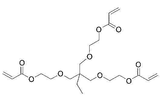
含フッ素化合物C
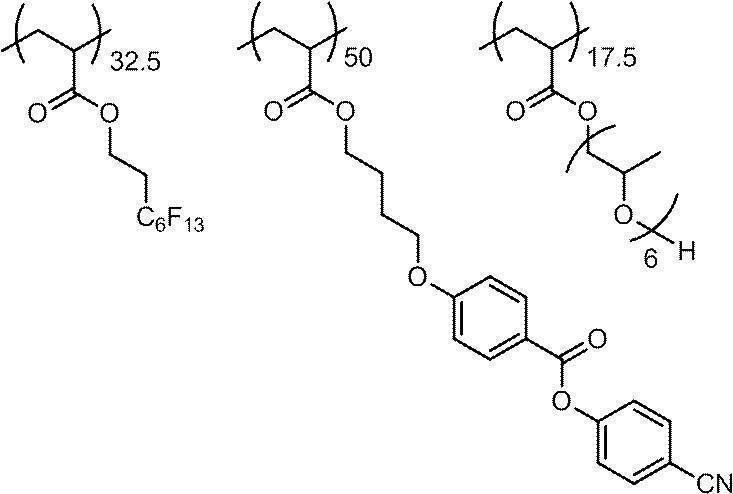
密着改良剤2

次いで、上記で調製した光学異方性層(C1)の塗布液Cを上記作製した片面保護膜付き偏光板01の偏光子側の面に、#2.0のワイヤーバーを用いて塗布し、乾燥した。70℃で90秒加熱して、ディスコティック液晶性化合物を配向させた。
その後、ただちに70℃の温度条件で、290mJ/cm2の紫外線を照射して、ディスコティック液晶性化合物を重合させ、配向状態を固定し、光学異方性層(C1)を形成した。形成した光学異方性層(C1)の厚みは1μmであった。光学異方性層の厚みはレーザー膜厚計にて計測した。
なお、光学異方性層(C1)をガラス基板上に実施例と同条件で形成させ、光学異方性層のみのレターデーションを測定したところ、Re(550)=0nm、Rth(550)=125nm、波長分散を示すRe(450)/Re(550)=1.09であった。屈折率はnx=1.58とした。
その後、ただちに70℃の温度条件で、290mJ/cm2の紫外線を照射して、ディスコティック液晶性化合物を重合させ、配向状態を固定し、光学異方性層(C1)を形成した。形成した光学異方性層(C1)の厚みは1μmであった。光学異方性層の厚みはレーザー膜厚計にて計測した。
なお、光学異方性層(C1)をガラス基板上に実施例と同条件で形成させ、光学異方性層のみのレターデーションを測定したところ、Re(550)=0nm、Rth(550)=125nm、波長分散を示すRe(450)/Re(550)=1.09であった。屈折率はnx=1.58とした。
〔光学異方性層(A1)の形成〕
次いで、光学異方性層(C1)の表面に、偏光子の吸収軸と直交方向にラビング処理を施した。ラビング処理面上に実施例3-1で調製した光学異方性層用塗布液Aのメチルエチルケトンを640質量部に変更し、バー番手#2.0のバーコーターを用いて塗布した。次いで、膜面温度110℃で30秒間加熱熟成し、その後ただちに、膜面温度60℃空気下にて空冷メタルハライドランプ(アイグラフィックス(株)製)を用いて、290mJ/cm2の紫外線を照射し、その配向状態を固定化することにより光学異方性層(A1)を形成することにより、視認側偏光板を作製した。
形成された光学異方性層(A1)は、棒状液晶が水平配向しており、遅相軸方向はラビング方向に平行、すなわち、遅相軸方向が偏光子の吸収軸方向に対して直交していた。このとき、光学異方性層の厚みは1μmであった。
なお、光学異方性層(A1)をガラス基板上に実施例と同条件で形成させ、光学異方性層のみのレターデーションを測定したところ、Re(550)=30nm、Rth(550)=15nm、波長分散を示すRe(450)/Re(550)=0.90であった。屈折率はnx=1.48とした。
次いで、光学異方性層(C1)の表面に、偏光子の吸収軸と直交方向にラビング処理を施した。ラビング処理面上に実施例3-1で調製した光学異方性層用塗布液Aのメチルエチルケトンを640質量部に変更し、バー番手#2.0のバーコーターを用いて塗布した。次いで、膜面温度110℃で30秒間加熱熟成し、その後ただちに、膜面温度60℃空気下にて空冷メタルハライドランプ(アイグラフィックス(株)製)を用いて、290mJ/cm2の紫外線を照射し、その配向状態を固定化することにより光学異方性層(A1)を形成することにより、視認側偏光板を作製した。
形成された光学異方性層(A1)は、棒状液晶が水平配向しており、遅相軸方向はラビング方向に平行、すなわち、遅相軸方向が偏光子の吸収軸方向に対して直交していた。このとき、光学異方性層の厚みは1μmであった。
なお、光学異方性層(A1)をガラス基板上に実施例と同条件で形成させ、光学異方性層のみのレターデーションを測定したところ、Re(550)=30nm、Rth(550)=15nm、波長分散を示すRe(450)/Re(550)=0.90であった。屈折率はnx=1.48とした。
〔バックライト側偏光板〕
視認側偏光板と同様の方法で、バックライト側偏光板を作製した。
視認側偏光板と同様の方法で、バックライト側偏光板を作製した。
〔液晶表示装置の作製および評価〕
実施例1-1と同様の方法により、実施例4-1の液晶表示装置を作製した。
作製した液晶表示装置について、実施例1-1と同様の方法により評価した。その結果を表5に記載した。
実施例1-1と同様の方法により、実施例4-1の液晶表示装置を作製した。
作製した液晶表示装置について、実施例1-1と同様の方法により評価した。その結果を表5に記載した。
<実施例4-2>
〔光学異方性層(C1)の形成〕
実施例4-1の光学異方性層(C1)の作製において、メチルエチルケトンを122質量部に変更した以外は実施例4-1と同様にして、下記表5に示す厚みおよび光学特性(Re、Rthおよび波長分散)を有する光学異方性層(C1)を形成した。
〔光学異方性層(C1)の形成〕
実施例4-1の光学異方性層(C1)の作製において、メチルエチルケトンを122質量部に変更した以外は実施例4-1と同様にして、下記表5に示す厚みおよび光学特性(Re、Rthおよび波長分散)を有する光学異方性層(C1)を形成した。
〔光学異方性層(A1)の形成〕
実施例4-1の光学異方性層(A1)の作製において、メチルエチルケトンを566質量部に変更し、#1.2のワイヤーバーに変更した以外は、実施例4-1と同様にして、下記表5に示す厚みおよび光学特性(Re、Rthおよび波長分散)を有する光学異方性層(A1)を作製した。
実施例4-1の光学異方性層(A1)の作製において、メチルエチルケトンを566質量部に変更し、#1.2のワイヤーバーに変更した以外は、実施例4-1と同様にして、下記表5に示す厚みおよび光学特性(Re、Rthおよび波長分散)を有する光学異方性層(A1)を作製した。
〔視認側およびバックライト側の偏光板の作製〕
上記光学異方性層(C1)および光学異方性層(A1)を用いた以外は、実施例4-1と同様の方法で、視認側およびバックライト側の偏光板を作製した。
上記光学異方性層(C1)および光学異方性層(A1)を用いた以外は、実施例4-1と同様の方法で、視認側およびバックライト側の偏光板を作製した。
〔液晶表示装置の作製、評価〕
上記で作製した偏光板を用いた以外は、実施例1-1と同様にして液晶表示装置を作製し、評価を行った。
上記で作製した偏光板を用いた以外は、実施例1-1と同様にして液晶表示装置を作製し、評価を行った。
<実施例4-3>
〔光学異方性層(C1)の形成〕
実施例4-1の光学異方性層(C1)の作製において、メチルエチルケトンを162質量部に変更した以外は、実施例4-1と同様にして、下記表5に示す厚みおよび光学特性(Re、Rthおよび波長分散)を有する光学異方性層(C1)を形成した。
〔光学異方性層(C1)の形成〕
実施例4-1の光学異方性層(C1)の作製において、メチルエチルケトンを162質量部に変更した以外は、実施例4-1と同様にして、下記表5に示す厚みおよび光学特性(Re、Rthおよび波長分散)を有する光学異方性層(C1)を形成した。
〔光学異方性層(A1)の形成〕
実施例4-1の光学異方性層(A1)の作製において、メチルエチルケトンを454質量部に変更し、#2.0のワイヤーバーに変更した以外は実施例4-1と同様にして、下記表5に示す厚みおよび光学特性(Re、Rthおよび波長分散)を有する光学異方性層(A1)を作製した。
実施例4-1の光学異方性層(A1)の作製において、メチルエチルケトンを454質量部に変更し、#2.0のワイヤーバーに変更した以外は実施例4-1と同様にして、下記表5に示す厚みおよび光学特性(Re、Rthおよび波長分散)を有する光学異方性層(A1)を作製した。
〔視認側およびバックライト側の偏光板の作製〕
上記光学異方性層(C1)および光学異方性層(A1)を用いた以外は、実施例4-1と同様の方法で、視認側およびバックライト側の偏光板を作製した。
上記光学異方性層(C1)および光学異方性層(A1)を用いた以外は、実施例4-1と同様の方法で、視認側およびバックライト側の偏光板を作製した。
〔液晶表示装置の作製、評価〕
上記で作製した偏光板を用いた以外は、実施例1-1と同様にして液晶表示装置を作製し、評価を行った。
上記で作製した偏光板を用いた以外は、実施例1-1と同様にして液晶表示装置を作製し、評価を行った。
<実施例4-4>
〔光学異方性層(C1)の形成〕
実施例4-1の光学異方性層(C1)の作製において、メチルエチルケトンを218質量部に変更した以外は実施例4-1と同様にして、下記表5に示す厚みおよび光学特性(Re、Rthおよび波長分散)を有する光学異方性層(C1)を形成した。
〔光学異方性層(C1)の形成〕
実施例4-1の光学異方性層(C1)の作製において、メチルエチルケトンを218質量部に変更した以外は実施例4-1と同様にして、下記表5に示す厚みおよび光学特性(Re、Rthおよび波長分散)を有する光学異方性層(C1)を形成した。
〔光学異方性層(A1)の形成〕
実施例4-1の光学異方性層(A1)の作製において、メチルエチルケトンを343質量部に変更し、#2.0のワイヤーバーに変更した以外は、実施例4-1と同様にして、下記表5に示す厚みおよび光学特性(Re、Rthおよび波長分散)を有する光学異方性層(A1)を作製した。
実施例4-1の光学異方性層(A1)の作製において、メチルエチルケトンを343質量部に変更し、#2.0のワイヤーバーに変更した以外は、実施例4-1と同様にして、下記表5に示す厚みおよび光学特性(Re、Rthおよび波長分散)を有する光学異方性層(A1)を作製した。
〔視認側およびバックライト側の偏光板の作製〕
上記光学異方性層(C1)および光学異方性層(A1)を用いた以外は、実施例4-1と同様の方法で、視認側およびバックライト側の偏光板を作製した。
上記光学異方性層(C1)および光学異方性層(A1)を用いた以外は、実施例4-1と同様の方法で、視認側およびバックライト側の偏光板を作製した。
〔液晶表示装置の作製、評価〕
上記で作製した偏光板を用いた以外は、実施例1-1と同様にして液晶表示装置を作製し、評価を行った。
上記で作製した偏光板を用いた以外は、実施例1-1と同様にして液晶表示装置を作製し、評価を行った。
<実施例4-5>
〔光学異方性層(C1)の形成〕
ゼオノア1430R(ノルボルネン系開環重合体水素化物、日本ゼオン社製、Tg138℃)のペレットを単軸押出機(三菱重工社製:シリンダー内径が90mm、スクリューのL/Dが25)で温度240℃で溶融し、厚さ45μmの透明樹脂を得た。次いでゾーン加熱の縦一軸(MD)延伸装置とテンター延伸(横一軸(TD)延伸)装置に順次送り込んで逐次二軸延伸を行い、下記表5に示す厚みおよび光学特性(Re、Rthおよび波長分散)を有する光学異方性層(C1)を得た。延伸温度は縦延伸、横延伸のいずれも140℃、延伸倍率はMD方向に30%、TD方向に30%とした。屈折率はnx=1.52として光学特性を測定した。
〔光学異方性層(C1)の形成〕
ゼオノア1430R(ノルボルネン系開環重合体水素化物、日本ゼオン社製、Tg138℃)のペレットを単軸押出機(三菱重工社製:シリンダー内径が90mm、スクリューのL/Dが25)で温度240℃で溶融し、厚さ45μmの透明樹脂を得た。次いでゾーン加熱の縦一軸(MD)延伸装置とテンター延伸(横一軸(TD)延伸)装置に順次送り込んで逐次二軸延伸を行い、下記表5に示す厚みおよび光学特性(Re、Rthおよび波長分散)を有する光学異方性層(C1)を得た。延伸温度は縦延伸、横延伸のいずれも140℃、延伸倍率はMD方向に30%、TD方向に30%とした。屈折率はnx=1.52として光学特性を測定した。
〔光学異方性層(A1)の形成〕
実施例4-1と同様にして、下記表5に示す厚みおよび光学特性(Re、Rthおよび波長分散)を有する光学異方性層を作製した。
実施例4-1と同様にして、下記表5に示す厚みおよび光学特性(Re、Rthおよび波長分散)を有する光学異方性層を作製した。
〔視認側およびバックライト側の偏光板の作製〕
上記光学異方性層(C1)および光学異方性層(A1)を用いた以外は、実施例4-1と同様の方法で、視認側およびバックライト側の偏光板を作製した。
上記光学異方性層(C1)および光学異方性層(A1)を用いた以外は、実施例4-1と同様の方法で、視認側およびバックライト側の偏光板を作製した。
〔液晶表示装置の作製、評価〕
上記で作製した偏光板を用いた以外は、実施例1-1と同様にして液晶表示装置を作製し、評価を行った。
上記で作製した偏光板を用いた以外は、実施例1-1と同様にして液晶表示装置を作製し、評価を行った。
<実施例4-6>
実施例1-7で作製した片面保護膜付き偏光板02を用いた以外は、実施例4-1と同様にして液晶表示装置を作製し、評価を行った。
実施例1-7で作製した片面保護膜付き偏光板02を用いた以外は、実施例4-1と同様にして液晶表示装置を作製し、評価を行った。
<実施例4-7>
実施例1-8で作製した片面保護膜付き偏光板03を用いた以外は、実施例4-1と同様にして液晶表示装置を作製し、評価を行った。
実施例1-8で作製した片面保護膜付き偏光板03を用いた以外は、実施例4-1と同様にして液晶表示装置を作製し、評価を行った。
<実施例4-8>
実施例1-9で作製した片面保護膜付き偏光板04を用いた以外は、実施例4-1と同様にして液晶表示装置を作製し、評価を行った。
実施例1-9で作製した片面保護膜付き偏光板04を用いた以外は、実施例4-1と同様にして液晶表示装置を作製し、評価を行った。
<実施例4-9>
実施例1-10で作製した片面保護膜付き偏光板05を用いた以外は、実施例4-1と同様にして液晶表示装置を作製し、評価を行った。
実施例1-10で作製した片面保護膜付き偏光板05を用いた以外は、実施例4-1と同様にして液晶表示装置を作製し、評価を行った。
<比較例6>
〔光学異方性層(C1)の形成〕
実施例4-1の光学異方性層(C1)の作製において、メチルエチルケトンを88質量部に変更した以外は、実施例4-1と同様にして、下記表5に示す厚みおよび光学特性(Re、Rthおよび波長分散)を有する光学異方性層(C1)を形成した。
〔光学異方性層(C1)の形成〕
実施例4-1の光学異方性層(C1)の作製において、メチルエチルケトンを88質量部に変更した以外は、実施例4-1と同様にして、下記表5に示す厚みおよび光学特性(Re、Rthおよび波長分散)を有する光学異方性層(C1)を形成した。
〔光学異方性層(A1)の形成〕
実施例4-1の光学異方性層(A1)の作製において、メチルエチルケトンを1569質量部に変更し、#1.2のワイヤーバーに変更した以外は実施例4-1と同様にして、下記表5に示す厚みおよび光学特性(Re、Rthおよび波長分散)を有する光学異方性層(A1)を作製した。
実施例4-1の光学異方性層(A1)の作製において、メチルエチルケトンを1569質量部に変更し、#1.2のワイヤーバーに変更した以外は実施例4-1と同様にして、下記表5に示す厚みおよび光学特性(Re、Rthおよび波長分散)を有する光学異方性層(A1)を作製した。
〔視認側およびバックライト側の偏光板の作製〕
上記光学異方性層(C1)および光学異方性層(A1)を用いた以外は、実施例4-1と同様の方法で、視認側およびバックライト側の偏光板を作製した。
上記光学異方性層(C1)および光学異方性層(A1)を用いた以外は、実施例4-1と同様の方法で、視認側およびバックライト側の偏光板を作製した。
〔液晶表示装置の作製、評価〕
上記で作製した偏光板を用いた以外は、実施例1-1と同様にして液晶表示装置を作製し、評価を行った。
上記で作製した偏光板を用いた以外は、実施例1-1と同様にして液晶表示装置を作製し、評価を行った。
<比較例7>
〔光学異方性層(C1)の形成〕
実施例4-1の光学異方性層(C1)の作製において、メチルエチルケトンを333質量部に変更した以外は実施例4-1と同様にして下記表5に示す厚みおよび光学特性(Re、Rthおよび波長分散)を有する光学異方性層(C1)を形成した。
〔光学異方性層(C1)の形成〕
実施例4-1の光学異方性層(C1)の作製において、メチルエチルケトンを333質量部に変更した以外は実施例4-1と同様にして下記表5に示す厚みおよび光学特性(Re、Rthおよび波長分散)を有する光学異方性層(C1)を形成した。
〔光学異方性層(A1)の形成〕
実施例4-1の光学異方性層(A1)の作製において、メチルエチルケトンを491質量部に変更し、#4.0のワイヤーバーに変更した以外は実施例4-1と同様にして下記表5に示す厚みおよび光学特性(Re、Rthおよび波長分散)を有する光学異方性層(A1)を作製した。
実施例4-1の光学異方性層(A1)の作製において、メチルエチルケトンを491質量部に変更し、#4.0のワイヤーバーに変更した以外は実施例4-1と同様にして下記表5に示す厚みおよび光学特性(Re、Rthおよび波長分散)を有する光学異方性層(A1)を作製した。
〔視認側およびバックライト側の偏光板の作製〕
上記光学異方性層(C1)および光学異方性層(A1)を用いた以外は、実施例4-1と同様の方法で、視認側およびバックライト側の偏光板を作製した。
上記光学異方性層(C1)および光学異方性層(A1)を用いた以外は、実施例4-1と同様の方法で、視認側およびバックライト側の偏光板を作製した。
〔液晶表示装置の作製、評価〕
上記で作製した偏光板を用いた以外は、実施例1-1と同様にして液晶表示装置を作製し、評価を行った。
上記で作製した偏光板を用いた以外は、実施例1-1と同様にして液晶表示装置を作製し、評価を行った。
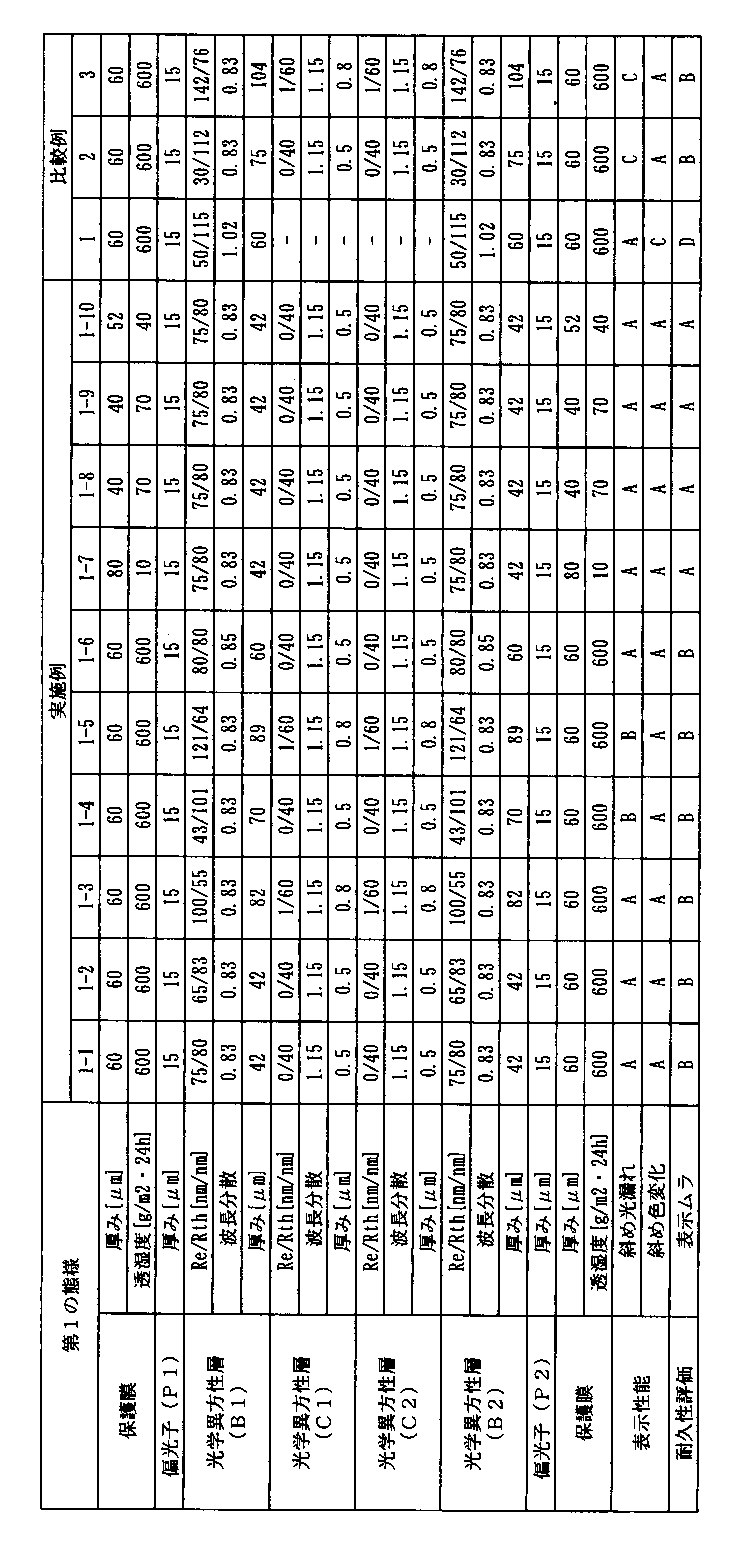


表2~表5に示す結果から、垂直配向モード液晶セルを所定の関係式を満たす光学特性を有する2枚(視認側およびバックライト側で各1枚)の光学異方性層で光学補償し、かつ、視認側偏光子およびバックライト側偏光子のそれぞれを所定の関係式を満たす光学性を有する光学異方性層で光学補償することにより、液晶表示装置を薄型化した場合であっても表示性能に優れ、温湿度環境変化に対する耐久性に優れることが分かった(実施例1-1~実施例1-10、実施例2-1~実施例2-10、実施例3-1~実施例3-10、実施例4-1~実施例4-9)。
特に、保護膜の透湿度が100g/m2/24h以下であると、表示ムラがより低減し、耐久性が更に向上していることが分かった(実施例1-7~実施例1-10、実施例2-7~実施例2-10、実施例3-7~実施例3-10、実施例4-6~実施例4-9)。
特に、保護膜の透湿度が100g/m2/24h以下であると、表示ムラがより低減し、耐久性が更に向上していることが分かった(実施例1-7~実施例1-10、実施例2-7~実施例2-10、実施例3-7~実施例3-10、実施例4-6~実施例4-9)。
1 偏光子(P1)
2 光学異方性層(B1)
3 光学異方性層(C1)
4,14 保護膜
5,15 ラミネートフィルム
6 光学異方性層(A1)
10 視認側偏光板
11 偏光子(P2)
12 光学異方性層(B2)
13 光学異方性層(C2)
16 光学異方性層(A2)
20 垂直配向モード液晶セル
30 バックライト側偏光板
40 液晶表示装置
2 光学異方性層(B1)
3 光学異方性層(C1)
4,14 保護膜
5,15 ラミネートフィルム
6 光学異方性層(A1)
10 視認側偏光板
11 偏光子(P2)
12 光学異方性層(B2)
13 光学異方性層(C2)
16 光学異方性層(A2)
20 垂直配向モード液晶セル
30 バックライト側偏光板
40 液晶表示装置
Claims (18)
- 視認側からバックライト側の方向に、第1の偏光子(P1)、第1の光学異方性層(B1)、第1の液晶性化合物を有する光学異方性層(C1)、垂直配向モード液晶セル、第2の液晶性化合物を有する光学異方性層(C2)、第2の光学異方性層(B2)、および、第2の偏光子(P2)をこの順に有し、
前記偏光子(P1)および前記偏光子(P2)が、それぞれの吸収軸を互いに直交にして配置され、
前記光学異方性層(C1)および前記光学異方性層(C2)の厚みが、いずれも10μm以下であり、
前記光学異方性層(C1)および前記光学異方性層(C2)が、いずれも下記式(1-1)および(1-2)を満たし、
Re(550)≦30nm 式(1-1)
10nm≦Rth(550)≦100nm 式(1-2)
前記光学異方性層(B1)および前記光学異方性層(B2)が、いずれも下記式(1-3)、(1-4)、(1-5)、(1-6)および(1-7)を満たす、液晶表示装置。
20nm≦Re(550)≦160nm 式(1-3)
20nm≦Rth(550)≦160nm 式(1-4)
Rth(550)≧(-9)×Re(550)+400nm 式(1-5)
Rth(550)≦(-9/5)×Re(550)+310nm 式(1-6)
Re(450)/Re(550)≦1.05 式(1-7)
ただし、Re(λ)は、波長λnmにおける面内レターデーションを表し、Rth(λ)は、波長λnmにおける厚み方向のレターデーションを表す。 - 視認側からバックライト側の方向に、第1の偏光子(P1)、第1の液晶性化合物を有する光学異方性層(C1)、第1の光学異方性層(B1)、垂直配向モード液晶セル、第2の光学異方性層(B2)、第2の液晶性化合物を有する光学異方性層(C2)、および、第2の偏光子(P2)をこの順に有し、
前記偏光子(P1)および前記偏光子(P2)が、それぞれの吸収軸を互いに直交にして配置され、
前記光学異方性層(C1)および前記光学異方性層(C2)の厚みが、いずれも10μm以下であり、
前記光学異方性層(C1)および前記光学異方性層(C2)が、いずれも下記式(2-1)および(2-2)を満たし、
Re(550)≦30nm 式(2-1)
30nm≦Rth(550)≦120nm 式(2-2)
前記光学異方性層(B1)および前記光学異方性層(B2)が、いずれも下記式(2-3)、(2-4)および(2-5)を満たす、液晶表示装置。
15nm≦Re(550)≦70nm 式(2-3)
20nm≦Rth(550)≦120nm 式(2-4)
Re(450)/Re(550)≦1.1 式(2-5)
ただし、Re(λ)は、波長λnmにおける面内レターデーションを表し、Rth(λ)は、波長λnmにおける厚み方向のレターデーションを表す。 - 視認側からバックライト側の方向に、第1の偏光子(P1)、第1の液晶性化合物を有する光学異方性層(A1)、第1の光学異方性層(C1)、垂直配向モード液晶セル、第2の光学異方性層(C2)、第2の液晶性化合物を有する光学異方性層(A2)、および、第2の偏光子(P2)をこの順に有し、
前記偏光子(P1)および前記偏光子(P2)が、それぞれの吸収軸を互いに直交にして配置され、
前記光学異方性層(A1)および前記光学異方性層(A2)の厚みが、いずれも10μm以下であり、
前記光学異方性層(A1)および前記光学異方性層(A2)が、いずれも下記式(3-1)、(3-2)および(3-3)を満たし、
50nm≦Re(550)≦130 式(3-1)
20nm≦Rth(550)≦70 式(3-2)
Re(450)/Re(550)≦1.05 式(3-3)
前記光学異方性層(C1)および前記光学異方性層(C2)が、いずれも下記式(3-4)および(3-5)を満たす、液晶表示装置。
Re(550)≦30nm 式(3-4)
20nm≦Rth(550)≦120 式(3-5)
ただし、Re(λ)は、波長λnmにおける面内レターデーションを表し、Rth(λ)は、波長λnmにおける厚み方向のレターデーションを表す。 - 視認側からバックライト側の方向に、第1の偏光子(P1)、第1の光学異方性層(C1)、第1の液晶性化合物を有する光学異方性層(A1)、垂直配向モード液晶セル、第2の液晶性化合物を有する光学異方性層(A2)、第2の光学異方性層(C2)、および、第2の偏光子(P2)をこの順に有し、
前記偏光子(P1)および前記偏光子(P2)が、それぞれの吸収軸を互いに直交にして配置され、
前記光学異方性層(A1)および前記光学異方性層(A2)の厚みが、いずれも10μm以下であり、
前記光学異方性層(A1)および前記光学異方性層(A2)が、いずれも下記式(4-1)、(4-2)および(4-3)を満たし、
10nm≦Re(550)≦70nm 式(4-1)
0nm≦Rth(550)≦40nm 式(4-2)
Re(450)/Re(550)≦1.05 式(4-3)
前記光学異方性層(C1)および前記光学異方性層(C2)が、いずれも下記式(4-4)および(4-5)を満たす、液晶表示装置。
Re(550)≦30nm 式(4-4)
70nm≦Rth(550)≦180nm 式(4-5)
ただし、Re(λ)は、波長λnmにおける面内レターデーションを表し、Rth(λ)は、波長λnmにおける厚み方向のレターデーションを表す。 - 前記光学異方性層(C1)および前記光学異方性層(C2)が含有する前記液晶性化合物が、いずれもディスコティック液晶性化合物であり、
前記光学異方性層(C1)および前記光学異方性層(C2)が、いずれも下記式(5)を満たす、請求項1または2に記載の液晶表示装置。
0.9<Re40(450)/Re40(550)≦1.2 式(5)
ただし、Re40(λ)は、波長λnmにおける極角40°から測定したレターデーションを表す。 - 前記光学異方性層(C1)および前記光学異方性層(C2)が、いずれもディスコティック液晶性化合物を含有し、
前記光学異方性層(C1)および前記光学異方性層(C2)が、いずれも下記式(5)を満たす、請求項3または4に記載の液晶表示装置。
0.9<Re40(450)/Re40(550)≦1.2 式(5)
ただし、Re40(λ)は、波長λnmにおける極角40°から測定したレターデーションを表す。 - 前記光学異方性層(A1)および前記光学異方性層(A2)が含有する前記液晶性化合物が、いずれも棒状液晶性化合物である、請求項3、4および6のいずれか1項に記載の液晶表示装置。
- 前記光学異方性層(A1)および前記光学異方性層(A2)が、いずれも下記式(6)を満たす、請求項7に記載の液晶表示装置。
Re(450)/Re(550)<1.0 式(6)
ただし、Re(λ)は、波長λnmにおける面内レターデーションを表す。 - 前記偏光子(P1)と前記光学異方性層(C1)とが隣接し、前記偏光子(P2)と前記光学異方性層(C2)とが隣接している、請求項2に記載の液晶表示装置。
- 前記偏光子(P1)と前記光学異方性層(A1)とが隣接し、前記偏光子(P2)と前記光学異方性層(A2)とが隣接している、請求項3に記載の液晶表示装置。
- 前記偏光子(P1)と前記光学異方性層(C1)とが配向膜を介して積層され、前記偏光子(P2)と前記光学異方性層(C2)とが配向膜を介して積層されている、請求項2に記載の液晶表示装置。
- 前記偏光子(P1)と前記光学異方性層(A1)とが配向膜を介して積層され、前記偏光子(P2)と前記光学異方性層(A2)とが配向膜を介して積層されている、請求項3に記載の液晶表示装置。
- 前記偏光子(P1)と前記光学異方性層(C1)とが接着剤層または粘着剤層を介して積層され、前記偏光子(P2)と前記光学異方性層(C2)とが接着剤層または粘着剤層を介して積層されている、請求項2に記載の液晶表示装置。
- 前記偏光子(P1)と前記光学異方性層(A1)とが接着剤層または粘着剤層を介して積層され、前記偏光子(P2)と前記光学異方性層(A2)とが接着剤層または粘着剤層を介して積層されている、請求項3に記載の液晶表示装置。
- 前記偏光子(P1)の視認側および前記偏光子(P2)のバックライト側のいずれか一方または両方に保護膜を有し、
前記保護膜の透湿度が、100g/m2/24h以下である、請求項1~14のいずれか1項に記載の液晶表示装置。 - 前記光学異方性層(A1)、前記光学異方性層(A2)、前記光学異方性層(B1)、前記光学異方性層(B2)、前記光学異方性層(C1)、および、前記光学異方性層(C2)からなる群から選択される少なくとも1つの光学異方性層の透湿度が、50g/m2/24h以下である、請求項1~15のいずれか1項に記載の液晶表示装置。
- 前記偏光子(P1)の視認側および前記偏光子(P2)のバックライト側のいずれか一方または両方にラミネートフィルムを有し、
前記ラミネートフィルムの透湿度が、30g/m2/24h以下である、請求項1~14のいずれか1項に記載の液晶表示装置。 - 前記偏光子(P1)および前記偏光子(P2)の少なくとも一方の厚さが、25μm以下である、請求項1~17のいずれか1項に記載の液晶表示装置。
Priority Applications (1)
| Application Number | Priority Date | Filing Date | Title |
|---|---|---|---|
| JP2016507822A JPWO2015137446A1 (ja) | 2014-03-13 | 2015-03-12 | 液晶表示装置 |
Applications Claiming Priority (2)
| Application Number | Priority Date | Filing Date | Title |
|---|---|---|---|
| JP2014-050749 | 2014-03-13 | ||
| JP2014050749 | 2014-03-13 |
Publications (1)
| Publication Number | Publication Date |
|---|---|
| WO2015137446A1 true WO2015137446A1 (ja) | 2015-09-17 |
Family
ID=54071883
Family Applications (1)
| Application Number | Title | Priority Date | Filing Date |
|---|---|---|---|
| PCT/JP2015/057294 Ceased WO2015137446A1 (ja) | 2014-03-13 | 2015-03-12 | 液晶表示装置 |
Country Status (3)
| Country | Link |
|---|---|
| JP (1) | JPWO2015137446A1 (ja) |
| TW (1) | TW201539092A (ja) |
| WO (1) | WO2015137446A1 (ja) |
Cited By (6)
| Publication number | Priority date | Publication date | Assignee | Title |
|---|---|---|---|---|
| WO2016143885A1 (ja) * | 2015-03-12 | 2016-09-15 | 日東電工株式会社 | 偏光フィルムおよびその製造方法、光学フィルムならびに画像表示装置 |
| JP2016170412A (ja) * | 2015-03-12 | 2016-09-23 | 日東電工株式会社 | 偏光フィルムおよびその製造方法、光学フィルムならびに画像表示装置 |
| WO2016171041A1 (ja) * | 2015-04-24 | 2016-10-27 | 日本ゼオン株式会社 | 複層フィルムの製造方法及び複層フィルム |
| CN108603035A (zh) * | 2016-03-09 | 2018-09-28 | 日东电工株式会社 | 固化性树脂组合物、偏振膜及其制造方法、光学膜以及图像显示装置 |
| KR20200046111A (ko) * | 2017-09-15 | 2020-05-06 | 도요보 가부시키가이샤 | 편광자 보호 필름, 편광판 및 액정 표시 장치 |
| CN118420818A (zh) * | 2024-04-28 | 2024-08-02 | 拓烯科技(衢州)有限公司 | 环烯烃共聚物、制备方法及其在虚拟现实级头戴式显示器中的应用 |
Citations (8)
| Publication number | Priority date | Publication date | Assignee | Title |
|---|---|---|---|---|
| JP2003344660A (ja) * | 2002-05-29 | 2003-12-03 | Fuji Photo Film Co Ltd | 位相差板およびその製法方法並びにそれを用いた円偏光板、液晶表示装置 |
| JP2006317747A (ja) * | 2005-05-13 | 2006-11-24 | Nitto Denko Corp | 偏光板、その製造方法、光学フィルムおよび画像表示装置 |
| JP2009015279A (ja) * | 2006-11-27 | 2009-01-22 | Nitto Denko Corp | 液晶パネルおよび液晶表示装置 |
| JP2009036860A (ja) * | 2007-07-31 | 2009-02-19 | Dainippon Printing Co Ltd | 液晶表示装置 |
| JP2009053614A (ja) * | 2007-08-29 | 2009-03-12 | Nitto Denko Corp | 積層光学フィルム、積層光学フィルムを用いた液晶パネルおよび液晶表示装置 |
| JP2010107941A (ja) * | 2008-07-08 | 2010-05-13 | Fujifilm Corp | Tnモード液晶表示装置、それに用いられる光学補償フィルムとその製造方法および偏光板 |
| JP2010256564A (ja) * | 2009-04-23 | 2010-11-11 | Sharp Corp | 偏光板上の表面処理の識別方法 |
| JP2011227508A (ja) * | 2011-06-06 | 2011-11-10 | Fujifilm Corp | 透明保護フィルム、光学補償フィルム、偏光板、及び液晶表示装置 |
-
2015
- 2015-03-12 TW TW104107845A patent/TW201539092A/zh unknown
- 2015-03-12 JP JP2016507822A patent/JPWO2015137446A1/ja not_active Abandoned
- 2015-03-12 WO PCT/JP2015/057294 patent/WO2015137446A1/ja not_active Ceased
Patent Citations (8)
| Publication number | Priority date | Publication date | Assignee | Title |
|---|---|---|---|---|
| JP2003344660A (ja) * | 2002-05-29 | 2003-12-03 | Fuji Photo Film Co Ltd | 位相差板およびその製法方法並びにそれを用いた円偏光板、液晶表示装置 |
| JP2006317747A (ja) * | 2005-05-13 | 2006-11-24 | Nitto Denko Corp | 偏光板、その製造方法、光学フィルムおよび画像表示装置 |
| JP2009015279A (ja) * | 2006-11-27 | 2009-01-22 | Nitto Denko Corp | 液晶パネルおよび液晶表示装置 |
| JP2009036860A (ja) * | 2007-07-31 | 2009-02-19 | Dainippon Printing Co Ltd | 液晶表示装置 |
| JP2009053614A (ja) * | 2007-08-29 | 2009-03-12 | Nitto Denko Corp | 積層光学フィルム、積層光学フィルムを用いた液晶パネルおよび液晶表示装置 |
| JP2010107941A (ja) * | 2008-07-08 | 2010-05-13 | Fujifilm Corp | Tnモード液晶表示装置、それに用いられる光学補償フィルムとその製造方法および偏光板 |
| JP2010256564A (ja) * | 2009-04-23 | 2010-11-11 | Sharp Corp | 偏光板上の表面処理の識別方法 |
| JP2011227508A (ja) * | 2011-06-06 | 2011-11-10 | Fujifilm Corp | 透明保護フィルム、光学補償フィルム、偏光板、及び液晶表示装置 |
Cited By (13)
| Publication number | Priority date | Publication date | Assignee | Title |
|---|---|---|---|---|
| WO2016143885A1 (ja) * | 2015-03-12 | 2016-09-15 | 日東電工株式会社 | 偏光フィルムおよびその製造方法、光学フィルムならびに画像表示装置 |
| JP2016170412A (ja) * | 2015-03-12 | 2016-09-23 | 日東電工株式会社 | 偏光フィルムおよびその製造方法、光学フィルムならびに画像表示装置 |
| JP2020122977A (ja) * | 2015-03-12 | 2020-08-13 | 日東電工株式会社 | 偏光フィルムおよびその製造方法、光学フィルムならびに画像表示装置 |
| WO2016171041A1 (ja) * | 2015-04-24 | 2016-10-27 | 日本ゼオン株式会社 | 複層フィルムの製造方法及び複層フィルム |
| JPWO2016171041A1 (ja) * | 2015-04-24 | 2018-02-15 | 日本ゼオン株式会社 | 複層フィルムの製造方法及び複層フィルム |
| CN108603035A (zh) * | 2016-03-09 | 2018-09-28 | 日东电工株式会社 | 固化性树脂组合物、偏振膜及其制造方法、光学膜以及图像显示装置 |
| KR20200054241A (ko) * | 2017-09-15 | 2020-05-19 | 도요보 가부시키가이샤 | 편광자 보호 필름, 편광판 및 액정 표시 장치 |
| KR20200046111A (ko) * | 2017-09-15 | 2020-05-06 | 도요보 가부시키가이샤 | 편광자 보호 필름, 편광판 및 액정 표시 장치 |
| JP2020144376A (ja) * | 2017-09-15 | 2020-09-10 | 東洋紡株式会社 | 偏光子保護フィルム、偏光板及び液晶表示装置 |
| KR102453214B1 (ko) * | 2017-09-15 | 2022-10-11 | 도요보 가부시키가이샤 | 편광자 보호 필름, 편광판 및 액정 표시 장치 |
| KR102468284B1 (ko) * | 2017-09-15 | 2022-11-17 | 도요보 가부시키가이샤 | 편광자 보호 필름, 편광판 및 액정 표시 장치 |
| JP7288878B2 (ja) | 2017-09-15 | 2023-06-08 | 東洋紡株式会社 | 偏光子保護フィルム、偏光板及び液晶表示装置 |
| CN118420818A (zh) * | 2024-04-28 | 2024-08-02 | 拓烯科技(衢州)有限公司 | 环烯烃共聚物、制备方法及其在虚拟现实级头戴式显示器中的应用 |
Also Published As
| Publication number | Publication date |
|---|---|
| TW201539092A (zh) | 2015-10-16 |
| JPWO2015137446A1 (ja) | 2017-04-06 |
Similar Documents
| Publication | Publication Date | Title |
|---|---|---|
| JP4618675B2 (ja) | 位相差フィルム、偏光素子、液晶パネルおよび液晶表示装置 | |
| US10025012B2 (en) | Polarizing plate and liquid crystal display device | |
| CN100410774C (zh) | 液晶面板、液晶电视和液晶显示装置 | |
| CN100392441C (zh) | 层叠光学薄膜、椭圆偏振片和图像显示装置 | |
| JP3851918B2 (ja) | 液晶パネルおよび液晶表示装置 | |
| TWI451171B (zh) | 光學補償薄膜、偏光板及液晶顯示裝置 | |
| WO2008068978A1 (ja) | 積層光学フィルム、積層光学フィルムを用いた液晶パネル、および液晶表示装置 | |
| US11987742B2 (en) | Polymerizable liquid crystal composition, cured product, optical film, polarizing plate, and image display device | |
| WO2015137446A1 (ja) | 液晶表示装置 | |
| JP5284567B2 (ja) | 液晶表示装置 | |
| TW202110620A (zh) | 偏光板及包括其的光學顯示裝置 | |
| WO2011065587A1 (en) | Va-mode liquid-crystal display device | |
| US7505099B2 (en) | Optical resin film and polarizing plate and liquid crystal display using same | |
| WO2011010751A1 (en) | Va-mode liquid-crystal display device | |
| TW200835980A (en) | Liquid crystal panel, and liquid crystal display | |
| TW200907510A (en) | Liquid crystal panel and liquid crystal display device | |
| JP2015072439A (ja) | 液晶表示装置 | |
| US7541074B2 (en) | Optical film and optical compensatory film, polarizing plate and liquid crystal display using same | |
| TWI797319B (zh) | 寬頻帶波長薄膜及其製造方法,以及圓偏光薄膜的製造方法 | |
| JP2009282140A (ja) | 画像表示パネル及びその製造方法 | |
| JP4744398B2 (ja) | 光学補償フィルム、偏光板及び液晶表示装置 | |
| JP4991207B2 (ja) | 光学フィルム、これを用いた光学補償フィルム、偏光板および液晶表示装置 | |
| JP6199716B2 (ja) | 位相差フィルムおよび液晶表示装置 | |
| JP2011085885A (ja) | Va液晶表示装置 | |
| CN100407000C (zh) | 液晶面板和液晶显示装置 |
Legal Events
| Date | Code | Title | Description |
|---|---|---|---|
| 121 | Ep: the epo has been informed by wipo that ep was designated in this application |
Ref document number: 15761873 Country of ref document: EP Kind code of ref document: A1 |
|
| ENP | Entry into the national phase |
Ref document number: 2016507822 Country of ref document: JP Kind code of ref document: A |
|
| NENP | Non-entry into the national phase |
Ref country code: DE |
|
| 122 | Ep: pct application non-entry in european phase |
Ref document number: 15761873 Country of ref document: EP Kind code of ref document: A1 |