WO2015137251A1 - 圧電センサ - Google Patents
圧電センサ Download PDFInfo
- Publication number
- WO2015137251A1 WO2015137251A1 PCT/JP2015/056672 JP2015056672W WO2015137251A1 WO 2015137251 A1 WO2015137251 A1 WO 2015137251A1 JP 2015056672 W JP2015056672 W JP 2015056672W WO 2015137251 A1 WO2015137251 A1 WO 2015137251A1
- Authority
- WO
- WIPO (PCT)
- Prior art keywords
- sheet
- piezoelectric
- conductor
- electrode
- signal electrode
- Prior art date
- Legal status (The legal status is an assumption and is not a legal conclusion. Google has not performed a legal analysis and makes no representation as to the accuracy of the status listed.)
- Ceased
Links
Images




Classifications
-
- G—PHYSICS
- G01—MEASURING; TESTING
- G01L—MEASURING FORCE, STRESS, TORQUE, WORK, MECHANICAL POWER, MECHANICAL EFFICIENCY, OR FLUID PRESSURE
- G01L1/00—Measuring force or stress, in general
- G01L1/16—Measuring force or stress, in general using properties of piezoelectric devices
-
- H—ELECTRICITY
- H10—SEMICONDUCTOR DEVICES; ELECTRIC SOLID-STATE DEVICES NOT OTHERWISE PROVIDED FOR
- H10N—ELECTRIC SOLID-STATE DEVICES NOT OTHERWISE PROVIDED FOR
- H10N30/00—Piezoelectric or electrostrictive devices
- H10N30/30—Piezoelectric or electrostrictive devices with mechanical input and electrical output, e.g. functioning as generators or sensors
- H10N30/302—Sensors
-
- H—ELECTRICITY
- H10—SEMICONDUCTOR DEVICES; ELECTRIC SOLID-STATE DEVICES NOT OTHERWISE PROVIDED FOR
- H10N—ELECTRIC SOLID-STATE DEVICES NOT OTHERWISE PROVIDED FOR
- H10N30/00—Piezoelectric or electrostrictive devices
- H10N30/80—Constructional details
- H10N30/85—Piezoelectric or electrostrictive active materials
- H10N30/857—Macromolecular compositions
-
- H—ELECTRICITY
- H10—SEMICONDUCTOR DEVICES; ELECTRIC SOLID-STATE DEVICES NOT OTHERWISE PROVIDED FOR
- H10N—ELECTRIC SOLID-STATE DEVICES NOT OTHERWISE PROVIDED FOR
- H10N30/00—Piezoelectric or electrostrictive devices
- H10N30/80—Constructional details
- H10N30/87—Electrodes or interconnections, e.g. leads or terminals
-
- H—ELECTRICITY
- H10—SEMICONDUCTOR DEVICES; ELECTRIC SOLID-STATE DEVICES NOT OTHERWISE PROVIDED FOR
- H10N—ELECTRIC SOLID-STATE DEVICES NOT OTHERWISE PROVIDED FOR
- H10N30/00—Piezoelectric or electrostrictive devices
- H10N30/80—Constructional details
- H10N30/87—Electrodes or interconnections, e.g. leads or terminals
- H10N30/875—Further connection or lead arrangements, e.g. flexible wiring boards, terminal pins
-
- H—ELECTRICITY
- H10—SEMICONDUCTOR DEVICES; ELECTRIC SOLID-STATE DEVICES NOT OTHERWISE PROVIDED FOR
- H10N—ELECTRIC SOLID-STATE DEVICES NOT OTHERWISE PROVIDED FOR
- H10N30/00—Piezoelectric or electrostrictive devices
- H10N30/80—Constructional details
- H10N30/88—Mounts; Supports; Enclosures; Casings
- H10N30/883—Additional insulation means preventing electrical, physical or chemical damage, e.g. protective coatings
Definitions
- the present invention relates to a piezoelectric sensor.
- Patent Document 1 discloses a piezoelectric body made of a polymer material, and a first electrode holding portion that is disposed on one side of the piezoelectric body and that has a signal electrode supported on a first insulator. And a second electrode carrying portion disposed on the other side of the piezoelectric body and carrying a ground electrode on a second insulator, the piezoelectric body, the first electrode carrying portion, and the second electrode carrying portion.
- the signal electrode is disposed within the region of the piezoelectric body, and the entire piezoelectric body is disposed within the region of the ground electrode or overlaps the region of the ground electrode when viewed in the overlapping direction with the electrode carrier.
- a piezoelectric sensor is disclosed.
- Patent Document 1 as a specific structure of the piezoelectric sensor, a signal electrode and a shield electrode are laminated and integrated in this order on the first surface of the piezoelectric body, and on the second surface of the piezoelectric body.
- a piezoelectric sensor in which ground electrodes are laminated and integrated is disclosed.
- a shield electrode is usually laminated and integrated on the signal electrode.
- Patent Document 1 a first electrode sheet in which electrodes are laminated and integrated on a first surface of an insulating sheet and a second electrode sheet in which electrodes are stacked and integrated on both sides of an insulating sheet are separately prepared.
- the piezoelectric sensor is manufactured by laminating and integrating the first electrode sheet on the first surface of the piezoelectric sensor via the adhesive layer and laminating and integrating the second electrode sheet on the second surface of the piezoelectric sensor. Therefore, the manufacturing process is complicated.
- the present invention provides a piezoelectric sensor that has a simplified structure and can be easily manufactured.
- the piezoelectric sensor of the present invention includes a piezoelectric sheet, a signal electrode laminated and integrated on the first surface of the piezoelectric sheet, and covers the signal electrode in a state of being electrically disconnected from the signal electrode, and a part thereof is grounded. It has a conductor acting as an electrode, a first conductive line electrically connected to the signal electrode, and a second conductive line electrically connected to the conductor.
- the conductor is formed of a single conductive sheet.
- the conductor is formed in a bag shape.
- the conductor is laminated on the second surface of the piezoelectric sheet.
- the piezoelectric sheet includes a polyolefin resin.
- the piezoelectric sheet is a foam sheet.
- the piezoelectric sensor of the present invention has the above-described configuration, and a signal electrode is covered with a conductor that partially acts as a ground electrode. Therefore, the piezoelectric sensor of the present invention uses a part of the conductor as the shield electrode of the signal electrode and the other part of the conductor as the ground electrode, which simplifies the structure and can be easily manufactured. .
- the piezoelectric sensor A includes a piezoelectric sheet 11, a signal electrode 12 laminated and integrated on the first surface of the piezoelectric sheet 11, and the signal electrode 12 electrically non-conductive. Electrically connected to the signal electrode 12 and the conductor 13 that covers the signal electrode 12 in the connected state, and that partly acts as a ground electrode, and the potential generated in the piezoelectric sheet 11 can be measured through the signal electrode 12
- the first conductive wire 14 and the second conductive wire 15 electrically connected to the conductor 13 are provided.
- the piezoelectric sheet 11 is not particularly limited as long as it is a sheet (a sheet having a piezoelectric phenomenon) that can generate charges on the surface when an external force is applied, but it can accurately detect weak biological signals such as pulse waves.
- the piezoelectric sheet is preferably a piezoelectric sheet in which a synthetic resin sheet (synthetic resin foam sheet or synthetic resin non-foamed sheet) is polarized, because it is highly sensitive and easily generates charges due to deformation in the thickness direction. Is more preferable, and a piezoelectric sheet obtained by imparting polarization to a synthetic resin foam sheet containing a polyolefin resin is particularly preferable.
- the synthetic resin constituting the synthetic resin sheet is not particularly limited, and examples thereof include polyolefin resins such as polyethylene resins and polypropylene resins, polyvinylidene fluoride, polylactic acid, and liquid crystal resins, and polyolefin resins are preferable. .
- the method for imparting polarization to the synthetic resin sheet is not particularly limited, and examples thereof include the following three methods.
- a synthetic resin sheet is sandwiched between a pair of flat plate electrodes, a flat plate electrode that is in contact with the surface to be charged is connected to a high-voltage DC power supply, the other flat plate electrode is grounded, and the synthetic resin is And a polarization step of applying polarization to the synthetic resin sheet by applying a DC or pulsed high voltage to the sheet to inject charges into the synthetic resin.
- the second method is to impart polarization to the synthetic resin sheet by irradiating the surface of the synthetic resin sheet with ionizing radiation such as electron beam and X-ray and ultraviolet rays, and ionizing air molecules in the vicinity of the synthetic resin sheet. It is a method to do.
- a grounded flat plate electrode is placed in close contact with the first surface of the synthetic resin sheet, and a predetermined interval is placed on the second surface side of the synthetic resin sheet so that a DC high-voltage power supply is electrically connected.
- a needle-like electrode or wire electrode connected to each other a corona discharge is generated by electric field concentration near the tip of the needle-like electrode or the surface of the wire electrode, and air molecules are ionized to cause the needle-like electrode or wire
- air ions generated by the polarity of the electrode are repelled to polarize the synthetic resin.
- the signal electrode 12 is laminated and integrated on the first surface 11a of the piezoelectric sheet 11 through a fixing agent layer (not shown) as necessary.
- the signal electrode 12 is not particularly limited as long as it has conductivity, and examples thereof include metal sheets such as copper foil and aluminum foil, and conductive films.
- the conductive film may be formed on the electrical insulating sheet and then laminated and integrated on the piezoelectric sheet 11, or the first surface 11a of the piezoelectric sheet 11 It may be formed directly.
- a method for forming a conductive film on an electrical insulating sheet or piezoelectric sheet for example, (1) Applying a conductive paste containing conductive fine particles in a binder on an electrical insulating sheet or piezoelectric sheet, and drying And (2) a method of forming an electrode by vapor deposition on an electrical insulating sheet or piezoelectric sheet.
- the electrical insulating sheet is not particularly limited as long as it has electrical insulating properties, and examples thereof include a polyimide sheet, a polyethylene terephthalate sheet, a polyethylene naphthalate sheet, and a polyvinyl chloride sheet.
- the fixing agent constituting the fixing agent layer is composed of a reaction system, solvent system, water system, hot melt system adhesive or pressure sensitive adhesive, and has a low dielectric constant from the viewpoint of maintaining the sensitivity of the piezoelectric sheet 11.
- a fixative is preferred.
- a part 13a of the conductor 13 which is not in contact with the signal electrode 12 and is not electrically connected thereto is formed on the entire surface of the signal electrode 12. It is arrange
- a portion 13a of the conductor 13 acts as a shield electrode.
- a part 13b of the conductor 13 is laminated on the second surface 11b of the piezoelectric sheet 11 (the surface opposite to the surface on which the signal electrode 12 is laminated and integrated).
- the conductor 13 is disposed on the second surface 11b of the piezoelectric sheet 11, so that a portion 13b functions as a ground electrode.
- the potential generated by the piezoelectric phenomenon in the piezoelectric sheet 11 can be measured through the signal electrode 12 using the ground electrode as a reference electrode.
- the conductor 13 is not particularly limited as long as it has conductivity. However, a sheet shape is preferable, and examples thereof include a metal foil, a metal net, and a conductive sheet having a conductive film on the surface. When using a conductive sheet having a conductive film on the surface, the conductive film is disposed on the piezoelectric sheet 11 side.
- the conductive sheet having a conductive film on the surface can be produced, for example, in the same manner as the method for forming a conductive film on the above-described electrical insulating sheet. Further, a part 13b of the conductor 13 may be laminated and integrated with the piezoelectric sheet 11 via the fixing agent layer.
- an electrical insulating sheet 16 is laminated and integrated on the entire surface of the signal electrode 12 of the piezoelectric sheet 11 so as to surround the piezoelectric sheet 11.
- One sheet of the conductor 13 is wound.
- the conductive film is on the piezoelectric sheet 11 side.
- the sheet-like conductor 13 is not in contact with the signal electrode 12 and is not electrically connected to the signal electrode 12.
- the sheet-like conductor 13 is preferably not in contact with the end face 11c of the piezoelectric sheet 11 because the charge generated in the piezoelectric sheet 11 can be detected more accurately.
- the sheet-like conductor 13 is laminated on the second surface 11b of the piezoelectric sheet 11.
- a portion 13 a of the conductor 13 covering the signal electrode 12 functions as a shield electrode for the signal electrode 12.
- the portion 13b laminated on the second surface 11b of the piezoelectric sheet 11 acts as a ground electrode and serves as a reference electrode when measuring the potential generated in the piezoelectric sheet 11 through the signal electrode 12. Since the conductor 13 surrounds the piezoelectric sheet 11 by making a single turn, the signal electrode 12 is almost completely shielded from electromagnetic waves from the outside by the conductor 13, and the electric potential generated in the piezoelectric sheet 11 is further increased. It can be measured accurately.
- the shield electrode and the ground electrode are configured by the sheet-like conductor 13 disposed so as to surround the piezoelectric sheet 11, the configuration of the piezoelectric sensor A is simple and easy. Can be manufactured. Further, the piezoelectric sensor A can be configured with fewer components, and the piezoelectric sensor A is thin and excellent in lightness.
- the case where the conductor 13 is formed in a sheet shape and the sheet-like conductor 13 is wound around the piezoelectric sheet 11 has been described.
- the piezoelectric sheet 11 may be accommodated in the bag-shaped conductor 13 and a part of the bag-shaped conductor 13 may be laminated on the piezoelectric sheet 11.
- a portion 13a of the bag-like conductor 13 that covers the signal electrode 12 functions as a shield electrode of the signal electrode 12.
- the portion 13a covering the signal electrode 12 is laminated on the signal electrode 12 via the electrical insulating sheet 16, and is not electrically connected to the signal electrode 12.
- the portion 13b disposed on the second surface 11b of the piezoelectric sheet 11 acts as a ground electrode.
- the potential generated by the piezoelectric phenomenon in the piezoelectric sheet 11 can be measured through the signal electrode 12 using the ground electrode as a reference electrode.
- the bag-like conductor 13 is preferably not in contact with the end surface 11c of the piezoelectric sheet 11 because the charge generated in the piezoelectric sheet 11 can be detected more accurately.
- one opening portion 133 is formed by integrating the outer peripheral edge portions except for one side of the flat rectangular surface portion 131 and the flat rectangular back surface portion 132. The bag-shaped conductor which has is mentioned.
- the bag-shaped conductor is composed of, for example, a metal foil, a metal net, a conductive sheet having a conductive film on the surface, and the like.
- the bag-shaped conductor is configured so that the conductive film is on the inside.
- the portion 13b of the bag-like conductor 13 laminated on the second surface 11b of the piezoelectric sheet 11 may be laminated and integrated on the piezoelectric sheet 11 via the fixing agent layer.
- the sheet-like conductor 13 is wound around the piezoelectric sheet 11 has been described.
- the sheet-like conductor 13 is bent from the central portion, and the conductor 13 is bent.
- the signal electrode 12 is entirely covered by one half, and a portion 13a covering the signal electrode 12 is used as a shield electrode of the signal electrode 12, and the other half of the conductor 13 is formed by the piezoelectric sheet 11 (preferably the piezoelectric sheet 11). May be laminated on the second surface 11b).
- the other half of the conductor 13 acts as a ground electrode by being laminated on the second surface 11b of the piezoelectric sheet 11.
- the potential generated by the piezoelectric phenomenon in the piezoelectric sheet 11 can be measured through the signal electrode 12 using the ground electrode as a reference electrode. Also in this case, it is preferable that the sheet-like conductor 13 is not in contact with the end face 11c of the piezoelectric sheet 11 because the charge generated in the piezoelectric sheet 11 can be detected more accurately.
- the other half of the conductor 13 may be laminated on the piezoelectric sheet 11 with the fixing agent layer interposed therebetween.
- first conductive wire 14 is electrically connected to the signal electrode 12, and the second conductive wire 15 is also electrically connected to the conductor 13.
- a general-purpose method may be used for connection of the first and second conductive wires 14 and 15 to the signal electrode 12 and the conductor 13.
- the first conductive wire 14 is connected to the measurement module, while the second conductive wire 15 is branched into two and one is connected to the measurement module to which the first conductive wire 14 is connected. And ground the other.
- the piezoelectric sheet 11 is compressed in the thickness direction, a positive charge and a negative charge held in a polarized state in the piezoelectric sheet are displaced relative to each other, thereby generating a charge on the surface of the piezoelectric sheet 11.
- the electric charge generated in the piezoelectric sheet 11 is measured as a potential through the signal electrode 12 using a ground electrode formed of a part 13b of the conductor 13 as a reference electrode.
- the conductor 13 has conductivity on the surface.
- the conductor 13 has the conductive layer 13c inside, the surface is electrically insulating layer 13d, It may be formed by 13d.
- the conductor 13 is formed in a sheet shape, and a conductive layer 13c such as a metal foil such as an aluminum foil or a deposited film, and both surfaces of the conductive layer 13c. Electrical insulating layers 13d and 13d laminated and integrated.
- the sheet-like conductor 13 whose surface is composed of the electrical insulating layers 13d and 13d is wound around the piezoelectric sheet 11 similarly to the piezoelectric sensor A shown in FIG.
- the portion 13c1 covers the entire surface of the signal electrode 12, and the other portion 13c2 of the conductive layer 13c in the sheet-like conductor 13 is laminated on the second surface 11b of the piezoelectric sheet 11.
- the electric insulating sheet for electrically isolating the signal electrode 12 and the electric conductor 13 on the signal electrode 12 Is not necessary.
- the following method is employed. Piercing the sheet-like conductor 13 through the pierce terminal 17 in the thickness direction, electrically connecting the portion 13c2 of the conductive layer 13c and the pierce terminal 17, and a portion of the conductive layer 13c through the pierce terminal 17 A portion 13c2 of the conductive layer 13c is made to act as a ground electrode by grounding the 13c2.
- the potential generated by the piezoelectric phenomenon in the piezoelectric sheet 11 can be measured through the signal electrode 12 using the ground electrode as a reference electrode.
- the conductor 13 may be formed in a bag shape. In order to make a part of the conductive layer of the bag-like conductor act as a ground electrode, for example, a pierce terminal may be used in the same manner as described above. Like the piezoelectric sensor A shown in FIG. 5, the conductor 13 is not wound around the piezoelectric sheet 11, and the sheet-like conductor 13 is folded in half.
- a piezoelectric sheet 11 may be disposed between the half portions. Specifically, as shown in FIG. 8, the sheet-like conductor 13 is bent from the center, and the signal electrode 12 is entirely covered with the half portion 13 c 1 of the conductive layer 13 c of the conductor 13. One half 13c1 of the conductive layer covering the signal electrode 12 is used as a shield electrode of the signal electrode 12. The other half 13c2 of the conductive layer 13c of the conductor 13 is laminated on the piezoelectric sheet 11 (preferably the second surface 11b of the piezoelectric sheet 11), and acts as a ground electrode in the same manner as described above. In this way, the piezoelectric sensor A may be configured.
- a pierce terminal may be used as described above.
- the same components as those of the piezoelectric sensor A shown in FIGS. 1 to 5 are denoted by the same reference numerals and description thereof is omitted.
- the piezoelectric sensor of the present invention can be suitably used as a sensor for detecting vibration.
- the sensor include a biological signal sensor for detecting a biological signal such as a pulse wave, respiration, and body movement, and a passage sensor for detecting vibration generated by a vehicle or a person traveling on the road.
- Piezoelectric sheet 12 Signal electrode 13
- Conductor 14 First conductive wire
- Second conductive wire Electrical insulation sheet 17 Pierce Terminal A Piezoelectric Sensor
Landscapes
- Physics & Mathematics (AREA)
- General Physics & Mathematics (AREA)
- Spectroscopy & Molecular Physics (AREA)
- Measuring Pulse, Heart Rate, Blood Pressure Or Blood Flow (AREA)
- Piezo-Electric Transducers For Audible Bands (AREA)
- Measuring Fluid Pressure (AREA)
- Force Measurement Appropriate To Specific Purposes (AREA)
Abstract
本発明は、構造が簡素化され且つ容易に製造することができる圧電センサを提供する。本発明の圧電センサAは、圧電シート11と、圧電シート11の第一の面に積層一体化されたシグナル電極12と、シグナル電極12と電気的に非接続状態にてシグナル電極12を覆い且つ圧電シート11に電気的に接続している導電体13と、シグナル電極12に電気的に接続された第一導電線14と、導電体13に電気的に接続された第二導電線15とを有していることを特徴とする。
Description
本発明は、圧電センサに関する。
従来から圧電シートを用いた圧電センサが提供されている。このような圧電センサとしては、特許文献1に、高分子材料からなる圧電体と、前記圧電体の一方の側に配置され、第1の絶縁体にシグナル電極を担持した第1の電極担持部と、前記圧電体の他方の側に配置され、第2の絶縁体にグランド電極を担持した第2の電極担持部とを備え、前記圧電体と前記第1の電極担持部と前記第2の電極担持部との重ね方向視において、前記シグナル電極が前記圧電体の領域内に収まり、且つ、前記圧電体全体が前記グランド電極の領域内に収まるかあるいは前記グランド電極の領域に重なり合うよう配置してある圧電センサが開示されている。
そして、特許文献1には、圧電センサの具体的な構造として、圧電体の第一の面にシグナル電極及びシールド電極がこの順序で積層一体化されていると共に、圧電体の第二の面にグランド電極が積層一体化されている圧電センサが開示されている。シグナル電極が外部からの電磁波の影響を受けないようにするために、通常、シグナル電極上にはシールド電極が積層一体化されている。
特許文献1においては、絶縁シートの第一の面に電極が積層一体化されてなる第一電極シートと、絶縁シートの両面に電極が積層一体化されてなる第二電極シートを別々に用意し、圧電センサの第一の面に第一電極シートを接着剤層を介して積層一体化すると共に、圧電センサの第二の面に第二電極シートを積層一体化することによって圧電センサが製造されており、製造工程が煩雑であるという問題点を有している。
本発明は、構造が簡素化され且つ容易に製造することができる圧電センサを提供する。
本発明の圧電センサは、圧電シートと、上記圧電シートの第一の面に積層一体化されたシグナル電極と、上記シグナル電極と電気的に非接続状態にて上記シグナル電極を覆い且つ一部分がグランド電極として作用する導電体と、上記シグナル電極に電気的に接続された第一導電線と、上記導電体に電気的に接続された第二導電線とを有していることを特徴とする。
上記圧電センサにおいて、導電体が一枚の導電シートから形成されていることを特徴とする。
上記圧電センサにおいて、導電体が袋状に形成されていることを特徴とする。
上記圧電センサにおいて、導電体が圧電シートの第二の面に積層されていることを特徴とする。
上記圧電センサにおいて、圧電シートがポリオレフィン系樹脂を含むことを特徴とする。
上記圧電センサにおいて、圧電シートが発泡シートであることを特徴とする。
本発明の圧電センサは、上述の如き構成を有しており、一部分がグランド電極として作用する導電体によってシグナル電極を覆っている。従って、本発明の圧電センサは、導電体の一部分をシグナル電極のシールド電極として、導電体の他の一部分をグランド電極として用いており、構造の簡素化を図っていると共に容易に製造可能である。
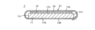
本発明の圧電センサの一例を図面を参照しながら説明する。圧電センサAは、図1及び図2に示したように、圧電シート11と、この圧電シート11の第一の面に積層一体化されたシグナル電極12と、上記シグナル電極12と電気的に非接続状態にてシグナル電極12を覆い且つ一部分がグランド電極として作用し圧電シート11にて発生した電位をシグナル電極12を通じて測定可能に配設された導電体13と、シグナル電極12に電気的に接続された第一導電線14と、導電体13に電気的に接続された第二導電線15とを有している。
圧電シート11としては、外力が加えられることによって表面に電荷を発生させることができるシート(圧電現象を有するシート)であれば、特に限定されないが、脈波などの微弱な生体信号を精度良く検出でき、感度が高く、厚み方向の変形で電荷を発生しやすいことから、合成樹脂シート(合成樹脂発泡シート又は合成樹脂非発泡シート)に分極を付与した圧電シートが好ましく、合成樹脂発泡シートに分極を付与した圧電シートがより好ましく、ポリオレフィン系樹脂を含む合成樹脂発泡シートに分極を付与した圧電シートが特に好ましい。
合成樹脂シートを構成する合成樹脂としては、特に限定されず、例えば、ポリエチレン系樹脂、ポリプロピレン系樹脂などのポリオレフィン系樹脂、ポリフッ化ビニリデン、ポリ乳酸、液晶樹脂などが挙げられ、ポリオレフィン系樹脂が好ましい。
合成樹脂シートに分極を付与する方法としては、特に限定されず、例えば、下記の3つの方法が挙げられる。第一の方法は、合成樹脂シートを一対の平板電極で挟持する挟持工程と、帯電させたい表面に接触させている平板電極を高圧直流電源に接続すると共に他方の平板電極をアースし、合成樹脂シートに直流又はパルス状の高電圧を印加して合成樹脂に電荷を注入して合成樹脂シートに分極を付与する分極工程とを含む方法である。第二の方法は、電子線、X線などの電離性放射線や紫外線を合成樹脂シートの表面に照射して、合成樹脂シートの近傍部の空気分子をイオン化することによって合成樹脂シートに分極を付与する方法である。第3の方法は、合成樹脂シートの第一の面に、アースされた平板電極を密着状態に重ね合わせ、合成樹脂シートの第二の面側に所定間隔を存して直流の高圧電源に電気的に接続された針状電極又はワイヤー電極を配設し、針状電極の先端又はワイヤー電極の表面近傍への電界集中によりコロナ放電を発生させ、空気分子をイオン化させて、針状電極又はワイヤー電極の極性により発生した空気イオンを反発させて合成樹脂に分極を付与する方法である。
圧電シート11の第一の面11aにはシグナル電極12が必要に応じて固定剤層(図示せず)を介して積層一体化されている。シグナル電極12は、導電性を有しておれば、特に限定されず、例えば、銅箔、アルミニウム箔などの金属シート、導電性膜などが挙げられる。
シグナル電極12を導電性膜で構成する場合、導電性膜は、電気絶縁シート上に形成された上で、圧電シート11上に積層一体化されもよいし、圧電シート11の第一の面11aに直接、形成されてもよい。電気絶縁シート又は圧電シート上に、導電性膜を形成する方法としては、例えば、(1)電気絶縁シート又は圧電シート上に、バインダー中に導電性微粒子を含有させてなる導電ペーストを塗布、乾燥させる方法、(2)電気絶縁シート又は圧電シート上に、蒸着によって電極を形成する方法などが挙げられる。
電気絶縁シートとしては、電気絶縁性を有しておれば、特に限定されず、例えば、ポリイミドシート、ポリエチレンテレフタレートシート、ポリエチレンナフタレートシート、ポリ塩化ビニルシートなどが挙げられる。
固定剤層を構成している固定剤は、反応系・溶剤系・水系・ホットメルト系の接着剤又は粘着剤から構成されており、圧電シート11の感度を維持する観点から、誘電率の低い固定剤が好ましい。
そして、圧電シート11上に積層一体化させているシグナル電極12上には、このシグナル電極12とは接触しておらず電気的に接続されていない導電体13の一部分13aがシグナル電極12を全面的に覆うように配設されている。導電体13の一部分13aはシールド電極として作用する。更に、上記導電体13の一部分13bが圧電シート11の第二の面11b(シグナル電極12が積層一体化されている面とは反対側の面)上に積層されている。導電体13は、圧電シート11の第二の面11b上に配設されることによって、一部分13bがグランド電極として作用する。圧電シート11にて圧電現象によって発生した電位は、グランド電極を基準電極としてシグナル電極12を通じて測定可能に構成されている。なお、導電体13としては、導電性を有しておれば、特に限定されないが、シート状が好ましく、例えば、金属箔、金属網、表面に導電性膜を有する導電性シートなどが挙げられる。表面に導電性膜を有する導電性シートを用いる場合は、導電性膜が圧電シート11側となるように配設される。表面に導電性膜を有する導電性シートは、例えば、上述した電気絶縁シート上に導電性膜を形成する方法と同様の要領で製造することができる。又、導電体13の一部分13bは、圧電シート11に上記固定剤層を介して積層一体化されていてもよい。
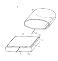
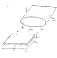
具体的には、図1及び図2に示したように、圧電シート11のシグナル電極12上には電気絶縁シート16が全面的に積層一体化されており、圧電シート11を包囲するように一枚のシート状の導電体13が一巻きされている。なお、シート状の導電体として表面に導電性膜を有する導電性シートを用いる場合には、導電性膜が圧電シート11側となるようにする。
シート状の導電体13はシグナル電極12に接触しておらずシグナル電極12とは電気的に接続していない。シート状の導電体13は、圧電シート11にて発生した電荷の検出がより正確となるので、圧電シート11の端面11cに接触していないことが好ましい。
一方、シート状の導電体13は、圧電シート11の第二の面11b上に積層されている。導電体13のうち、シグナル電極12を覆っている部分13aはシグナル電極12のシールド電極として作用する。圧電シート11の第二の面11b上に積層されている部分13bはグランド電極として作用し、圧電シート11にて発生した電位をシグナル電極12を通じて測定する際の基準電極となる。導電体13は、一巻きすることによって圧電シート11を包囲していることから、シグナル電極12は導電体13によって外部からの電磁波から略完全に遮蔽され、圧電シート11にて発生した電位をより正確に測定することができる。
このように、圧電シート11を包囲するようにして配設された一枚のシート状の導電体13によってシールド電極及びグランド電極を構成しているので、圧電センサAの構成が簡素であり且つ容易に製造することができる。又、圧電センサAを構成するにあたって構成部品の数が少なくてすみ、圧電センサAは厚みが薄く軽量性に優れている。
図1~3では、導電体13をシート状に形成し、シート状の導電体13を圧電シート11に巻いた場合を説明したが、図4に示したように、導電体13を予め袋状に形成し、袋状の導電体13内に圧電シート11を収納し、袋状の導電体13の一部分を圧電シート11上に積層させた構造としてもよい。この場合も、袋状の導電体13のうち、シグナル電極12を覆っている部分13aはシグナル電極12のシールド電極として作用する。シグナル電極12を覆っている部分13aは、電気絶縁シート16を介してシグナル電極12上に積層されており、シグナル電極12とは電気的に接続されていない。袋状の導電体13のうち、圧電シート11の第二の面11b上に配設され部分13bがグランド電極として作用する。圧電シート11にて圧電現象によって発生した電位は、グランド電極を基準電極としてシグナル電極12を通じて測定可能に構成されている。袋状の導電体13は、圧電シート11にて発生した電荷の検出がより正確となるので、圧電シート11の端面11cに接触していないことが好ましい。袋状の導電体13としては、例えば、平面矩形状の表面部131と平面矩形状の裏面部132とをこれらの一辺を除いた外周縁部同士を一体化することによって一個の開口部133を有する袋状の導電体が挙げられる。袋状の導電体は、例えば、金属箔、金属網、上述した表面に導電性膜を有する導電性シートなどから構成される。袋状の導電体を表面に導電性膜を有する導電性シートから構成する場合、導電性膜が内側となるように袋状の導電体が構成される。又、袋状の導電体13のうち、圧電シート11の第二の面11b上に積層された部分13bは、圧電シート11上に上記固定剤層を介して積層一体化されていてもよい。
又、図1では、シート状の導電体13を圧電シート11に一巻した場合を説明したが、図5に示したように、シート状の導電体13を中央部から屈曲させ、導電体13の一半部によってシグナル電極12を全面的に覆い、シグナル電極12を覆っている部分13aをシグナル電極12のシールド電極とすると共に、導電体13の他半部を圧電シート11(好ましくは圧電シート11の第二の面11b)上に積層させてもよい。導電体13の他半部は、圧電シート11の第二の面11b上に積層されることによってグランド電極として作用する。圧電シート11にて圧電現象によって発生した電位は、グランド電極を基準電極としてシグナル電極12を通じて測定可能に構成されている。この場合も、シート状の導電体13は、圧電シート11にて発生した電荷の検出がより正確となるので、圧電シート11の端面11cに接触していないことが好ましい。又、導電体13の他半部は、圧電シート11に上記固定剤層を介して積層されていてもよい。
更に、シグナル電極12には第一導電線14が電気的に接続されていると共に、導電体13にも第二導電線15が電気的に接続されている。なお、シグナル電極12及び導電体13への第一、第二導電線14、15の接続は汎用の方法が用いられればよい。
圧電センサAを使用するにあたっては、第一導電線14を測定モジュールに接続する一方、第二導電線15を二つに分岐して一方を第一導電線14を接続させている測定モジュールに接続させると共に他方にアースをとる。圧電シート11がその厚み方向に圧縮されると、圧電シート内に分極状態で保持された正電荷と負電荷が互いに相対変位することによって圧電シート11の表面に電荷が発生する。圧電シート11にて発生した電荷は電位として、導電体13の一部分13bから構成されたグランド電極を基準電極としてシグナル電極12を通じて測定される。
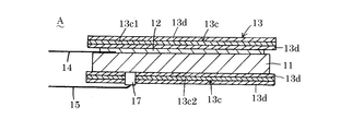
上記圧電センサAでは、導電体13はその表面において導電性を有している場合を説明したが、導電体13は、内部に導電層13cを有しておれば、表面が電気絶縁層13d、13dによって形成されていてもよい。
具体的には、図6及び図7に示したように、導電体13はシート状に形成されており、アルミニウム箔などの金属箔や蒸着膜などの導電層13cと、この導電層13cの両面に積層一体化された電気絶縁層13d、13dとを有している。
表面が電気絶縁層13d、13dから構成されたシート状の導電体13は、図1に示した圧電センサAと同様に圧電シート11に一巻きされ、シート状の導電体13における導電層13cの一部分13c1がシグナル電極12を全面的に覆っていると共に、シート状の導電体13における導電層13cの他の一部分13c2が圧電シート11の第二の面11b上に積層された状態となっている。なお、シート状の導電体13の表面は電気絶縁層13d、13dから構成されていることから、シグナル電極12上に、シグナル電極12と導電体13とを電気的に隔絶するための電気絶縁シートは必要ない。一方、シート状の導電体13の導電層13cの一部分13c2をグランド電極として作用させるために、例えば、下記の方法が採用される。シート状の導電体13にピアス端子17をその厚み方向に貫通した状態に打ち込み、導電層13cの一部分13c2とピアス端子17とを電気的に接続させ、ピアス端子17を介して導電層13cの一部分13c2にアースをとるなどして導電層13cの一部分13c2をグランド電極として作用させる。圧電シート11にて圧電現象によって発生した電位は、グランド電極を基準電極としてシグナル電極12を通じて測定可能に構成されている。又、導電体13の導電層13cと第二導電線15とは、ピアス端子17に第二導電線15を電気的に接続させることによって、第二導電線15と導電層13cとをピアス端子17を介して電気的に接続させればよい。又、図4に示した圧電センサAのように、導電体13は袋状に形成されていてもよい。袋状の導電体の導電層の一部分をグランド電極として作用させるために、例えば、上述と同様に、ピアス端子を用いればよい。図5に示した圧電センサAのように、導電体13は圧電シート11に一巻きされることなく、シート状の導電体13が二つ折り状態とされており、導電体13の一半部と他半部との間に圧電シート11が配設されていてもよい。具体的には、図8に示したように、シート状の導電体13を中央部から屈曲させ、導電体13の導電層13cの一半部13c1によってシグナル電極12を全面的に覆い、シグナル電極12を覆っている導電層の一半部13c1をシグナル電極12のシールド電極とする。導電体13の導電層13cの他半部13c2を圧電シート11(好ましくは圧電シート11の第二の面11b)上に積層して上述と同様の要領でグランド電極として作用させる。このようにして圧電センサAを構成してもよい。導電層13cの他半部13c2をグランド電極として作用させるために、例えば、上述と同様に、ピアス端子を用いればよい。図1~5に示した圧電センサAと同様の構成については同一符号を付してその説明を省略する。
(関連出願の相互参照)
本出願は、2014年3月10日に出願された日本国特許出願第2014-46330に基づく優先権を主張し、この出願の開示はこれらの全体を参照することにより本明細書に組み込まれる。
本出願は、2014年3月10日に出願された日本国特許出願第2014-46330に基づく優先権を主張し、この出願の開示はこれらの全体を参照することにより本明細書に組み込まれる。
本発明の圧電センサは、振動を検出するためのセンサとして好適に用いることができる。センサとしては、脈波、呼吸、体動などの生体信号を検出するための生体信号センサ、路上を通行する車両又は人によって生じる振動を検出する通行センサなどが挙げられる。
11 圧電シート
12 シグナル電極
13 導電体
14 第一導電線
15 第二導電線
16 電気絶縁シート
17 ピアス端子
A 圧電センサ
12 シグナル電極
13 導電体
14 第一導電線
15 第二導電線
16 電気絶縁シート
17 ピアス端子
A 圧電センサ
Claims (6)
- 圧電シートと、上記圧電シートの第一の面に積層一体化されたシグナル電極と、上記シグナル電極と電気的に非接続状態にて上記シグナル電極を覆い且つ一部分がグランド電極として作用する導電体と、上記シグナル電極に電気的に接続された第一導電線と、上記導電体に電気的に接続された第二導電線とを有していることを特徴とする圧電センサ。
- 導電体が一枚の導電シートから形成されていることを特徴とする請求項1に記載の圧電センサ。
- 導電体が袋状に形成されていることを特徴とする請求項1又は請求項2に記載の圧電センサ。
- 導電体が圧電シートの第二の面に積層されていることを特徴とする請求項1又は請求項2に記載の圧電センサ。
- 圧電シートがポリオレフィン系樹脂を含むことを特徴とする請求項1に記載の圧電センサ。
- 圧電シートが発泡シートであることを特徴とする請求項1に記載の圧電センサ。
Priority Applications (1)
| Application Number | Priority Date | Filing Date | Title |
|---|---|---|---|
| JP2015515064A JPWO2015137251A1 (ja) | 2014-03-10 | 2015-03-06 | 圧電センサ |
Applications Claiming Priority (2)
| Application Number | Priority Date | Filing Date | Title |
|---|---|---|---|
| JP2014046330 | 2014-03-10 | ||
| JP2014-046330 | 2014-03-10 |
Publications (1)
| Publication Number | Publication Date |
|---|---|
| WO2015137251A1 true WO2015137251A1 (ja) | 2015-09-17 |
Family
ID=54071697
Family Applications (1)
| Application Number | Title | Priority Date | Filing Date |
|---|---|---|---|
| PCT/JP2015/056672 Ceased WO2015137251A1 (ja) | 2014-03-10 | 2015-03-06 | 圧電センサ |
Country Status (3)
| Country | Link |
|---|---|
| JP (2) | JPWO2015137251A1 (ja) |
| TW (1) | TWI650537B (ja) |
| WO (1) | WO2015137251A1 (ja) |
Cited By (8)
| Publication number | Priority date | Publication date | Assignee | Title |
|---|---|---|---|---|
| US20150349744A1 (en) * | 2014-05-30 | 2015-12-03 | Kyocera Crystal Device Corporation | Crystal device and producing method of crystal device |
| WO2017126052A1 (ja) * | 2016-01-20 | 2017-07-27 | フジデノロ株式会社 | ホウ素中性子捕捉療法用システム |
| JP2018036060A (ja) * | 2016-08-29 | 2018-03-08 | 積水化学工業株式会社 | 圧電センサ構造体 |
| EP3694007A1 (en) * | 2019-02-05 | 2020-08-12 | Koninklijke Philips N.V. | Sensor comprising an interconnect having a carrier film |
| JP2020134444A (ja) * | 2019-02-25 | 2020-08-31 | ロボセンサー技研株式会社 | 圧電センサ |
| JP2021090695A (ja) * | 2019-12-12 | 2021-06-17 | 国立大学法人山形大学 | 生体情報検出装置 |
| EP3907769A1 (en) * | 2020-05-08 | 2021-11-10 | Koninklijke Philips N.V. | Sensor comprising an interconnect and an interventional medical device using the same |
| JPWO2020170962A1 (ja) * | 2019-02-18 | 2021-12-23 | 株式会社バルカー | 圧電センサーおよび圧電センサーの製造方法 |
Families Citing this family (1)
| Publication number | Priority date | Publication date | Assignee | Title |
|---|---|---|---|---|
| CN119827853A (zh) * | 2024-12-13 | 2025-04-15 | 北京中科飞龙传感技术有限责任公司 | 压电电极组件、加工方法及mems电场传感器 |
Citations (6)
| Publication number | Priority date | Publication date | Assignee | Title |
|---|---|---|---|---|
| JPH02179430A (ja) * | 1988-10-12 | 1990-07-12 | Polysens Spa | 動的力を検出するためのトランスジューサ及び、該トランスジューサを含み、計測及び/又は制御する装置及び方法 |
| JPH0875575A (ja) * | 1994-09-02 | 1996-03-22 | Matsushita Electric Ind Co Ltd | 圧電センサ |
| JP2001291906A (ja) * | 2000-04-07 | 2001-10-19 | Matsushita Electric Ind Co Ltd | 可撓性圧電素子 |
| JP2006253416A (ja) * | 2005-03-10 | 2006-09-21 | National Institute Of Advanced Industrial & Technology | スイッチング素子とスイッチング素子を用いた競泳用タッチ板 |
| JP2008304558A (ja) * | 2007-06-05 | 2008-12-18 | Erumekku Denshi Kogyo Kk | 圧電センサおよび電子弦楽器 |
| JP2009260063A (ja) * | 2008-04-17 | 2009-11-05 | Kaneka Corp | ポリフェニレンエーテル系発泡体からなるエレクトレット |
Family Cites Families (5)
| Publication number | Priority date | Publication date | Assignee | Title |
|---|---|---|---|---|
| US3894243A (en) * | 1974-06-06 | 1975-07-08 | Us Navy | Polymeric transducer array |
| JP2733441B2 (ja) * | 1994-03-01 | 1998-03-30 | 松下電器産業株式会社 | 在席検出装置 |
| JP2000277825A (ja) * | 1999-03-23 | 2000-10-06 | Tokai Rubber Ind Ltd | 圧電素子 |
| US6670866B2 (en) * | 2002-01-09 | 2003-12-30 | Nokia Corporation | Bulk acoustic wave resonator with two piezoelectric layers as balun in filters and duplexers |
| JP5083956B2 (ja) * | 2007-09-19 | 2012-11-28 | 独立行政法人産業技術総合研究所 | 詰まり検出システム |
-
2015
- 2015-03-06 JP JP2015515064A patent/JPWO2015137251A1/ja active Pending
- 2015-03-06 WO PCT/JP2015/056672 patent/WO2015137251A1/ja not_active Ceased
- 2015-03-10 TW TW104107486A patent/TWI650537B/zh active
-
2018
- 2018-11-21 JP JP2018218092A patent/JP6574889B2/ja active Active
Patent Citations (6)
| Publication number | Priority date | Publication date | Assignee | Title |
|---|---|---|---|---|
| JPH02179430A (ja) * | 1988-10-12 | 1990-07-12 | Polysens Spa | 動的力を検出するためのトランスジューサ及び、該トランスジューサを含み、計測及び/又は制御する装置及び方法 |
| JPH0875575A (ja) * | 1994-09-02 | 1996-03-22 | Matsushita Electric Ind Co Ltd | 圧電センサ |
| JP2001291906A (ja) * | 2000-04-07 | 2001-10-19 | Matsushita Electric Ind Co Ltd | 可撓性圧電素子 |
| JP2006253416A (ja) * | 2005-03-10 | 2006-09-21 | National Institute Of Advanced Industrial & Technology | スイッチング素子とスイッチング素子を用いた競泳用タッチ板 |
| JP2008304558A (ja) * | 2007-06-05 | 2008-12-18 | Erumekku Denshi Kogyo Kk | 圧電センサおよび電子弦楽器 |
| JP2009260063A (ja) * | 2008-04-17 | 2009-11-05 | Kaneka Corp | ポリフェニレンエーテル系発泡体からなるエレクトレット |
Cited By (17)
| Publication number | Priority date | Publication date | Assignee | Title |
|---|---|---|---|---|
| US20150349744A1 (en) * | 2014-05-30 | 2015-12-03 | Kyocera Crystal Device Corporation | Crystal device and producing method of crystal device |
| WO2017126052A1 (ja) * | 2016-01-20 | 2017-07-27 | フジデノロ株式会社 | ホウ素中性子捕捉療法用システム |
| US10668153B2 (en) | 2016-01-20 | 2020-06-02 | Fujidenolo Co. Ltd. | Boron neutron capture therapy system |
| JP2018036060A (ja) * | 2016-08-29 | 2018-03-08 | 積水化学工業株式会社 | 圧電センサ構造体 |
| JP7094457B2 (ja) | 2019-02-05 | 2022-07-01 | コーニンクレッカ フィリップス エヌ ヴェ | キャリアフィルムを有する相互接続を有するセンサ |
| WO2020160897A1 (en) * | 2019-02-05 | 2020-08-13 | Koninklijke Philips N.V. | Sensor comprising an interconnect having a carrier film |
| JP2022516811A (ja) * | 2019-02-05 | 2022-03-02 | コーニンクレッカ フィリップス エヌ ヴェ | キャリアフィルムを有する相互接続を有するセンサ |
| EP3694007A1 (en) * | 2019-02-05 | 2020-08-12 | Koninklijke Philips N.V. | Sensor comprising an interconnect having a carrier film |
| US12120961B2 (en) | 2019-02-05 | 2024-10-15 | Koninklijke Philips N.V. | Sensor comprising an interconnect having a carrier film |
| JPWO2020170962A1 (ja) * | 2019-02-18 | 2021-12-23 | 株式会社バルカー | 圧電センサーおよび圧電センサーの製造方法 |
| JP7391077B2 (ja) | 2019-02-18 | 2023-12-04 | 株式会社バルカー | 圧電センサーおよび圧電センサーの製造方法 |
| JP2020134444A (ja) * | 2019-02-25 | 2020-08-31 | ロボセンサー技研株式会社 | 圧電センサ |
| JP7519065B2 (ja) | 2019-02-25 | 2024-07-19 | ロボセンサー技研株式会社 | 圧電センサ |
| JP2021090695A (ja) * | 2019-12-12 | 2021-06-17 | 国立大学法人山形大学 | 生体情報検出装置 |
| JP7464247B2 (ja) | 2019-12-12 | 2024-04-09 | 国立大学法人山形大学 | 生体情報検出装置 |
| EP3907769A1 (en) * | 2020-05-08 | 2021-11-10 | Koninklijke Philips N.V. | Sensor comprising an interconnect and an interventional medical device using the same |
| WO2021224000A1 (en) * | 2020-05-08 | 2021-11-11 | Koninklijke Philips N.V. | Sensor comprising an interconnect and an interventional medical device using the same |
Also Published As
| Publication number | Publication date |
|---|---|
| JP2019056710A (ja) | 2019-04-11 |
| TW201534880A (zh) | 2015-09-16 |
| TWI650537B (zh) | 2019-02-11 |
| JP6574889B2 (ja) | 2019-09-11 |
| JPWO2015137251A1 (ja) | 2017-04-06 |
Similar Documents
| Publication | Publication Date | Title |
|---|---|---|
| JP6574889B2 (ja) | 圧電センサ | |
| TWI669370B (zh) | Pressure sensor | |
| JP6234858B2 (ja) | 圧電センサ | |
| JP6013120B2 (ja) | 圧電センサ | |
| JP6450197B2 (ja) | 生体検出システム | |
| JP6168891B2 (ja) | 生体信号センサシステム | |
| CN105036065B (zh) | 一种基于射线的驻极体极化装置及其极化方法 | |
| JP6279330B2 (ja) | 物体検出シート及びこれを用いた生体検出システム | |
| JP2017058344A (ja) | 圧電センサ構造 | |
| JP6294177B2 (ja) | 圧電センサ | |
| JP2015014550A (ja) | 圧電センサシート原反及び圧電素子 | |
| JP6328955B2 (ja) | 生体検出システム | |
| JP5545091B2 (ja) | 静電型スピーカ | |
| JP2014169945A (ja) | 圧電センサ | |
| JP2014170863A (ja) | 圧電センサの製造方法 | |
| JP6110267B2 (ja) | 圧電センサ構造体 | |
| JP6126388B2 (ja) | 生体信号センサ及びこれを用いた生体信号センサシステム | |
| JP2015068643A (ja) | 降雨検知システム | |
| JP2017062200A (ja) | 圧電センサ構造 | |
| JP6074331B2 (ja) | 圧電センサ | |
| JP2017151038A (ja) | 圧電センサ | |
| JP2015012987A (ja) | 生体信号センサ | |
| JP2014135308A (ja) | 圧電センサの製造方法 | |
| JP2018036060A (ja) | 圧電センサ構造体 | |
| JP2017067772A (ja) | 圧電センサ構造 |
Legal Events
| Date | Code | Title | Description |
|---|---|---|---|
| ENP | Entry into the national phase |
Ref document number: 2015515064 Country of ref document: JP Kind code of ref document: A |
|
| 121 | Ep: the epo has been informed by wipo that ep was designated in this application |
Ref document number: 15761449 Country of ref document: EP Kind code of ref document: A1 |
|
| NENP | Non-entry into the national phase |
Ref country code: DE |
|
| 122 | Ep: pct application non-entry in european phase |
Ref document number: 15761449 Country of ref document: EP Kind code of ref document: A1 |