WO2015128976A1 - データ記憶装置 - Google Patents
データ記憶装置 Download PDFInfo
- Publication number
- WO2015128976A1 WO2015128976A1 PCT/JP2014/054792 JP2014054792W WO2015128976A1 WO 2015128976 A1 WO2015128976 A1 WO 2015128976A1 JP 2014054792 W JP2014054792 W JP 2014054792W WO 2015128976 A1 WO2015128976 A1 WO 2015128976A1
- Authority
- WO
- WIPO (PCT)
- Prior art keywords
- memory module
- management unit
- volatile memory
- storage destination
- destination management
- Prior art date
Links
Images


Classifications
-
- G—PHYSICS
- G06—COMPUTING; CALCULATING OR COUNTING
- G06F—ELECTRIC DIGITAL DATA PROCESSING
- G06F3/00—Input arrangements for transferring data to be processed into a form capable of being handled by the computer; Output arrangements for transferring data from processing unit to output unit, e.g. interface arrangements
- G06F3/06—Digital input from, or digital output to, record carriers, e.g. RAID, emulated record carriers or networked record carriers
- G06F3/0601—Interfaces specially adapted for storage systems
- G06F3/0628—Interfaces specially adapted for storage systems making use of a particular technique
- G06F3/0629—Configuration or reconfiguration of storage systems
- G06F3/0631—Configuration or reconfiguration of storage systems by allocating resources to storage systems
-
- G—PHYSICS
- G06—COMPUTING; CALCULATING OR COUNTING
- G06F—ELECTRIC DIGITAL DATA PROCESSING
- G06F11/00—Error detection; Error correction; Monitoring
- G06F11/07—Responding to the occurrence of a fault, e.g. fault tolerance
- G06F11/14—Error detection or correction of the data by redundancy in operation
- G06F11/1402—Saving, restoring, recovering or retrying
- G06F11/1415—Saving, restoring, recovering or retrying at system level
- G06F11/142—Reconfiguring to eliminate the error
- G06F11/1428—Reconfiguring to eliminate the error with loss of hardware functionality
-
- G—PHYSICS
- G06—COMPUTING; CALCULATING OR COUNTING
- G06F—ELECTRIC DIGITAL DATA PROCESSING
- G06F11/00—Error detection; Error correction; Monitoring
- G06F11/07—Responding to the occurrence of a fault, e.g. fault tolerance
- G06F11/14—Error detection or correction of the data by redundancy in operation
- G06F11/1402—Saving, restoring, recovering or retrying
- G06F11/1415—Saving, restoring, recovering or retrying at system level
- G06F11/1441—Resetting or repowering
-
- G—PHYSICS
- G06—COMPUTING; CALCULATING OR COUNTING
- G06F—ELECTRIC DIGITAL DATA PROCESSING
- G06F12/00—Accessing, addressing or allocating within memory systems or architectures
- G06F12/02—Addressing or allocation; Relocation
- G06F12/08—Addressing or allocation; Relocation in hierarchically structured memory systems, e.g. virtual memory systems
- G06F12/0802—Addressing of a memory level in which the access to the desired data or data block requires associative addressing means, e.g. caches
- G06F12/0866—Addressing of a memory level in which the access to the desired data or data block requires associative addressing means, e.g. caches for peripheral storage systems, e.g. disk cache
-
- G—PHYSICS
- G06—COMPUTING; CALCULATING OR COUNTING
- G06F—ELECTRIC DIGITAL DATA PROCESSING
- G06F3/00—Input arrangements for transferring data to be processed into a form capable of being handled by the computer; Output arrangements for transferring data from processing unit to output unit, e.g. interface arrangements
- G06F3/06—Digital input from, or digital output to, record carriers, e.g. RAID, emulated record carriers or networked record carriers
- G06F3/0601—Interfaces specially adapted for storage systems
- G06F3/0602—Interfaces specially adapted for storage systems specifically adapted to achieve a particular effect
- G06F3/061—Improving I/O performance
-
- G—PHYSICS
- G06—COMPUTING; CALCULATING OR COUNTING
- G06F—ELECTRIC DIGITAL DATA PROCESSING
- G06F3/00—Input arrangements for transferring data to be processed into a form capable of being handled by the computer; Output arrangements for transferring data from processing unit to output unit, e.g. interface arrangements
- G06F3/06—Digital input from, or digital output to, record carriers, e.g. RAID, emulated record carriers or networked record carriers
- G06F3/0601—Interfaces specially adapted for storage systems
- G06F3/0602—Interfaces specially adapted for storage systems specifically adapted to achieve a particular effect
- G06F3/0614—Improving the reliability of storage systems
- G06F3/0619—Improving the reliability of storage systems in relation to data integrity, e.g. data losses, bit errors
-
- G—PHYSICS
- G06—COMPUTING; CALCULATING OR COUNTING
- G06F—ELECTRIC DIGITAL DATA PROCESSING
- G06F3/00—Input arrangements for transferring data to be processed into a form capable of being handled by the computer; Output arrangements for transferring data from processing unit to output unit, e.g. interface arrangements
- G06F3/06—Digital input from, or digital output to, record carriers, e.g. RAID, emulated record carriers or networked record carriers
- G06F3/0601—Interfaces specially adapted for storage systems
- G06F3/0628—Interfaces specially adapted for storage systems making use of a particular technique
- G06F3/0646—Horizontal data movement in storage systems, i.e. moving data in between storage devices or systems
- G06F3/0647—Migration mechanisms
-
- G—PHYSICS
- G06—COMPUTING; CALCULATING OR COUNTING
- G06F—ELECTRIC DIGITAL DATA PROCESSING
- G06F3/00—Input arrangements for transferring data to be processed into a form capable of being handled by the computer; Output arrangements for transferring data from processing unit to output unit, e.g. interface arrangements
- G06F3/06—Digital input from, or digital output to, record carriers, e.g. RAID, emulated record carriers or networked record carriers
- G06F3/0601—Interfaces specially adapted for storage systems
- G06F3/0668—Interfaces specially adapted for storage systems adopting a particular infrastructure
- G06F3/0671—In-line storage system
- G06F3/0683—Plurality of storage devices
- G06F3/0685—Hybrid storage combining heterogeneous device types, e.g. hierarchical storage, hybrid arrays
-
- H—ELECTRICITY
- H04—ELECTRIC COMMUNICATION TECHNIQUE
- H04L—TRANSMISSION OF DIGITAL INFORMATION, e.g. TELEGRAPHIC COMMUNICATION
- H04L45/00—Routing or path finding of packets in data switching networks
- H04L45/74—Address processing for routing
- H04L45/742—Route cache; Operation thereof
-
- G—PHYSICS
- G06—COMPUTING; CALCULATING OR COUNTING
- G06F—ELECTRIC DIGITAL DATA PROCESSING
- G06F2212/00—Indexing scheme relating to accessing, addressing or allocation within memory systems or architectures
- G06F2212/26—Using a specific storage system architecture
- G06F2212/261—Storage comprising a plurality of storage devices
-
- G—PHYSICS
- G06—COMPUTING; CALCULATING OR COUNTING
- G06F—ELECTRIC DIGITAL DATA PROCESSING
- G06F2212/00—Indexing scheme relating to accessing, addressing or allocation within memory systems or architectures
- G06F2212/28—Using a specific disk cache architecture
- G06F2212/285—Redundant cache memory
-
- G—PHYSICS
- G06—COMPUTING; CALCULATING OR COUNTING
- G06F—ELECTRIC DIGITAL DATA PROCESSING
- G06F2212/00—Indexing scheme relating to accessing, addressing or allocation within memory systems or architectures
- G06F2212/31—Providing disk cache in a specific location of a storage system
- G06F2212/313—In storage device
Definitions
- the present invention relates to a data storage device including a cache memory.
- a volatile memory module (an example of a cache memory) has been introduced into the memory system.
- the volatile memory module temporarily stores data in order to write data in parallel to a plurality of nonvolatile memory modules.
- the writing speed to the memory system may decrease or the system may stop.
- a path is determined by peer-to-peer communication in order to arbitrarily determine a path between many-to-many connected memory modules.
- An object of the present invention is to provide a many-to-many connection of memory modules without using a mechanism for centrally managing and controlling information such as data storage destinations and a crossbar switch circuit.
- a data storage device includes: A plurality of first memory modules for temporarily storing data; A first storage location manager provided in each first memory module; A plurality of second memory modules for storing data stored in each first memory module; A second storage destination management unit provided in each second memory module, The first memory module in which the first storage destination management unit provided in each first memory module and the second storage destination management unit provided in each second memory module communicate to store data Each time, determine the second memory module of the data transmission destination, Each of the first memory modules transmits data to the determined second memory module of the transmission destination.
- the path is determined by the storage destination management unit provided in each memory module. Therefore, it is not necessary to use a mechanism for managing and controlling information such as a data storage destination in a unified manner and a crossbar switch circuit.
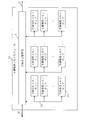
- FIG. 1 is a configuration diagram of a memory system 10 according to a first embodiment.
- the figure which shows the volatile memory management table 1446. 5 is a flowchart showing the operation of the memory system 10.
- FIG. Explanatory drawing of the failure information collection process of the volatile memory module 11.
- FIG. The block diagram of a HELLO packet.
- FIG. 1 is a configuration diagram of a volatile memory module 11.
- FIG. 1 is a configuration diagram of a nonvolatile memory module 12.
- FIG. 3 is a configuration diagram of a V storage destination management unit 13.
- FIG. 3 is a configuration diagram of an NV storage destination management unit 14.
- FIG. 1 is a configuration diagram of a memory system 10 (data storage device) according to the first embodiment.
- the memory system 10 includes a plurality of volatile memory modules 11 (first memory modules) and a plurality of nonvolatile memory modules 12 (second memory modules).
- Each volatile memory module 11 includes a V storage destination management unit 13 (first storage destination management unit).
- Each nonvolatile memory module 12 includes an NV storage destination management unit 14 (second storage destination management unit).
- Each volatile memory module 11 is, for example, a DRAM (Dynamic Random Access Memory) module
- each nonvolatile memory module 12 is, for example, a flash memory module.
- Each volatile memory module 11 is connected to an external input bus 15. Each volatile memory module 11 distributes and temporarily stores data input via the external input bus 15. Each volatile memory module 11 and each nonvolatile memory module 12 are connected by an inter-memory module bus 16. Since the number of ports of each volatile memory module 11 and each nonvolatile memory module 12 is limited, not all volatile memory modules 11 and all nonvolatile memory modules 12 are connected. Each nonvolatile memory module 12 is connected to an external output bus 17. Each nonvolatile memory module 12 stores data transmitted from the volatile memory module 11 via the inter-memory module bus 16. Each nonvolatile memory module 12 outputs the stored data via the external output bus 17.
- the V storage destination management unit 13 has a nonvolatile memory management table 1346
- the NV storage destination management unit 14 has a volatile memory management table 1446.
- the V storage destination management unit 13 and the NV storage destination management unit 14 communicate with each other to update the nonvolatile memory management table 1346 and the volatile memory management table 1446 to determine a data transfer path.
- Each volatile memory module 11 transmits the temporarily stored data to the nonvolatile memory module 12 indicated by the determined data transfer path.
- the performance (data writing speed) of the memory system 10 may be reduced due to a failure of the volatile memory module 11 or the nonvolatile memory module 12.
- the memory system 10 includes the volatile memory module 11 and the nonvolatile memory module 12 redundantly. That is, a part of the plurality of volatile memory modules 11 and a part of the plurality of nonvolatile memory modules 12 are in a standby state for backup.
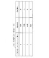
- FIG. 2 is a diagram showing the non-volatile memory management table 1346.
- the non-volatile memory management table 1346 has a non-volatile memory module number, failure information, and a connection request.
- the nonvolatile memory module number is an identifier of the nonvolatile memory module 12.
- the failure information is information indicating whether or not the nonvolatile memory module 12 has failed.
- the connection request is information indicating whether or not a connection request has been issued to the nonvolatile memory module 12.
- FIG. 3 is a diagram showing the volatile memory management table 1446.
- the volatile memory management table 1446 has a volatile memory module number, failure information, the number of paths, and usage right assignment.
- the volatile memory module number is an identifier of the volatile memory module 11.
- the failure information is information indicating whether or not the volatile memory module 11 has failed.
- the number of paths is the number of non-failed nonvolatile memory modules 12 connected to the volatile memory module 11.
- the usage right grant is information indicating whether or not the connection request is permitted.
- FIG. 4 is a flowchart showing the operation of the memory system 10.
- S1 Data input process
- Data is input to the memory system 10. Then, data is input to each volatile memory module 11 via the external input bus 15, and the data is distributed and stored in each volatile memory module 11.
- the V storage location management unit 13 of each volatile memory module 11 collects failure information of the nonvolatile memory module 12.
- FIG. 5 is an explanatory diagram of failure information collection processing of the nonvolatile memory module 12.
- the V storage destination management unit 13 of the volatile memory module 11 transmits a HELLO packet (survival confirmation message) to the NV storage destination management units 14 of all the connected nonvolatile memory modules 12 (1).
- the NV storage destination management unit 14 of the nonvolatile memory module 12 that has received the HELLO packet transmits a HELLO response packet to the V storage destination management unit 13 of the volatile memory module 11 (2).
- the V storage location management unit 13 of the volatile memory module 11 treats the non-volatile memory module 12 that has transmitted the HELLO response packet for the transmitted HELLO packet as operating (no failure).
- the V storage location management unit 13 of the volatile memory module 11 treats the nonvolatile memory module 12 that has not been transmitted within a predetermined time as not operating (failed). Then, the V storage location management unit 13 of the volatile memory module 11 updates the failure information in the nonvolatile memory management table 1346.
- the NV storage location management unit 14 of the nonvolatile memory module 12 collects failure information of the volatile memory module 11.
- FIG. 6 is an explanatory diagram of failure information collection processing of the volatile memory module 11.
- the NV storage destination management unit 14 of the nonvolatile memory module 12 transmits a HELLO packet to the V storage destination management units 13 of all the connected volatile memory modules 11 (1).
- the V storage destination management unit 13 of the volatile memory module 11 that has received the HELLO packet transmits a HELLO response packet to the NV storage destination management unit 14 of the nonvolatile memory module 12 (2).
- the NV storage destination management unit 14 of the non-volatile memory module 12 treats the volatile memory module 11 that has transmitted the HELLO response packet for the transmitted HELLO packet as operating (no failure).
- the NV storage destination management unit 14 of the nonvolatile memory module 12 treats the volatile memory module 11 that has not been transmitted within a predetermined time as not operating (failed). Then, the NV storage destination management unit 14 of the nonvolatile memory module 12 updates the failure information in the volatile memory management table 1446.
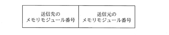
- FIG. 7 is a configuration diagram of a HELLO packet.
- the HELLO packet has a destination memory module number and a source memory module number.
- the memory module number of the transmission destination becomes the nonvolatile memory module number of the nonvolatile memory module 12 of the transmission destination, and the memory module of the transmission source The number becomes the volatile memory module number of the volatile memory module 11 of the transmission source.
- the memory module number of the transmission destination is the volatile memory module number of the volatile memory module 11 of the transmission destination, and the transmission source The memory module number is the non-volatile memory module number of the non-volatile memory module 12 that is the transmission source.
- FIG. 8 is a configuration diagram of the HELLO response packet.
- the HELLO response packet has a destination memory module number and a source memory module number. Since the memory module number of the transmission destination of the HELLO response packet and the memory module number of the transmission source are the same as in the case of the HELLO packet, description thereof is omitted.
- the first survival confirmation process in S2 and the second survival confirmation process in S3 are collectively referred to as a survival confirmation process.
- the V storage destination management unit 13 of the volatile memory module 11 in the standby state and the NV storage destination management unit 14 of the nonvolatile memory module 12 in the standby state perform the HELLO packet and the HELLO packet. Does not send a response packet.
- the V storage location management unit 13 of the volatile memory module 11 transmits a WAKEUP packet to the non-volatile memory module 12 in the standby state.
- the non-volatile memory module 12 in the standby state receives the WAKEUP packet
- the nonvolatile memory module 12 enters an operating state and transmits a HELLO packet and a HELLO response packet.
- the NV storage destination management unit 14 of the nonvolatile memory module 12 waits for a WAKEUP packet. Send to.
- the volatile memory module 11 in the standby state receives the WAKEUP packet, the volatile memory module 11 enters an operating state and transmits a HELLO packet and a HELLO response packet.
- the V storage destination management unit 13 of the volatile memory module 11 and the NV storage destination management unit 14 of the nonvolatile memory module 12 include failure information of the nonvolatile memory management table 1346, failure information of the volatile memory management table 1446, and The data transfer path is determined using the number of paths.
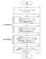
- FIG. 9 is an explanatory diagram of data transfer path determination processing.
- the V storage location management unit 13 of the volatile memory module 11 sequentially transmits a connection request packet (connection request message) to the nonvolatile memory module 12 indicating that the failure information in the nonvolatile memory management table 1346 is not failed. To do. For example, the V storage location management unit 13 of the volatile memory module 11 transmits connection request packets in ascending order of the nonvolatile memory module numbers. At this time, the V storage location management unit 13 of the volatile memory module 11 counts the number of nonvolatile memory modules 12 indicating that the failure information in the nonvolatile memory management table 1346 is not failed as the number of paths. Then, the V storage location management unit 13 of the volatile memory module 11 transmits the number of paths included in the connection request packet.
- the NV storage location management unit 14 of the nonvolatile memory module 12 transmits a connection response packet indicating permission or rejection for the connection request packet.
- the NV storage destination management unit 14 of the nonvolatile memory module 12 transmits a connection response packet (connection acknowledgment message) indicating permission to the connection request packet having the smallest number of paths among the received connection request packets, and the others.
- a connection response packet indicating rejection is transmitted. Note that connection request packets having the smallest number of paths may exist at the same rate.
- the NV storage destination management unit 14 of the nonvolatile memory module 12 transmits a connection response packet indicating permission to the connection request packet having the smallest volatile memory module number of the transmission source volatile memory module 11. .
- the NV storage location management unit 14 of the nonvolatile memory module 12 updates the number of paths in the volatile memory management table 1446 with the number of paths included in the received connection request packet.
- the NV storage destination management unit 14 of the nonvolatile memory module 12 updates the usage right assignment of the volatile memory management table 1446 according to the transmitted connection response packet.
- the V storage location management unit 13 of the volatile memory module 11 When receiving the connection response packet indicating permission, the V storage location management unit 13 of the volatile memory module 11 temporarily stops transmission of the connection request packet. On the other hand, when receiving the connection response packet indicating rejection, the V storage destination management unit 13 of the volatile memory module 11 transmits a connection request packet to the next nonvolatile memory module 12. When receiving the connection response packet, the V storage destination management unit 13 of the volatile memory module 11 updates the connection request in the nonvolatile memory management table 1346 for the nonvolatile memory module 12 that is the transmission source of the connection response packet. .
- connection response packet indicating permission when the connection request packet having a smaller number of paths is received, the connection response indicating permission is already displayed.
- a connection response packet (connection withdrawal message) indicating rejection is transmitted to the volatile memory module 11 that transmitted the packet.
- the NV storage destination management unit 14 of the nonvolatile memory module 12 transmits a connection response packet indicating permission to a connection request packet having a smaller number of paths.
- the V storage destination management unit 13 of the volatile memory module 11 that has received the connection response packet indicating rejection resumes transmission of the connection request packet that has been temporarily stopped.
- FIG. 10 is a configuration diagram of a connection request packet.
- the connection request packet includes a transmission destination nonvolatile memory module number, a transmission source volatile memory module number, and a volatile memory module path number.
- the destination nonvolatile memory module number is the nonvolatile memory module number of the destination nonvolatile memory module 12.
- the transmission source volatile memory module number is the volatile memory module number of the transmission source volatile memory module 11.
- the number of passes of the volatile memory module is the number of passes of the volatile memory module 11 as the transmission source.
- FIG. 11 is a configuration diagram of a connection response packet.
- the connection response packet includes a transmission destination volatile memory module number, a transmission source nonvolatile memory module number, and whether or not connection is possible.
- the destination volatile memory module number is the volatile memory module number of the destination volatile memory module 11.
- the transmission source nonvolatile memory module number is the nonvolatile memory module number of the transmission source nonvolatile memory module 12.
- the connectability is information indicating permission or rejection.
- FIG. 12 is a diagram showing the relationship among the nonvolatile memory management table 1346, the volatile memory management table 1446, the connection request packet, and the connection response packet.
- the nonvolatile memory module 12 in which the failure information in the nonvolatile memory management table 1346 is an operation and the connection request is not yet selected is selected as the transmission destination of the connection request packet.
- the number of volatile memory module paths in the connection request packet is the number of nonvolatile memory modules 12 on which failure information in the nonvolatile memory management table 1346 is operating.
- As the number of paths in the volatile memory management table 1446 the number of paths of the volatile memory module in the connection request packet is set. Based on the set number of paths, it is determined whether to grant (permit) usage rights or not (reject) usage rights. The determined use right grant is reflected in the connection availability of the connection response packet.
- the connection request in the nonvolatile memory management table 1346 is updated for the nonvolatile memory module 12 that is the transmission source of the connection response packet.
- each volatile memory module 11 transfers the data temporarily stored in S1 to the nonvolatile memory module 12 that is the transmission source of the connection response packet indicating the permission received in S4.
- each volatile memory module 11 can transfer data in parallel.
- FIG. 13 is a configuration diagram of the volatile memory module 11.
- the volatile memory module 11 includes a V storage location management unit 13 and one or more volatile memory chips 111.
- the V storage location management unit 13 and each volatile memory chip 111 are connected by a volatile memory bus 112.
- the data input via the external input bus 15 is transmitted to the V storage destination management unit 13, transmitted to the volatile memory chip 111 via the volatile memory bus 112, and temporarily stored.
- the V storage destination management unit 13 sequentially executes the above-described survival confirmation process and path determination process to determine the transmission destination nonvolatile memory module 12.
- the V storage location management unit 13 reads data temporarily stored in the volatile memory chip 111 and transmits the data to the determined nonvolatile memory module 12 via the inter-memory module bus 16.
- FIG. 14 is a configuration diagram of the nonvolatile memory module 12.
- the nonvolatile memory module 12 includes an NV storage destination management unit 14 and one or more nonvolatile memory chips 121.
- the NV storage destination management unit 14 and each nonvolatile memory chip 121 are connected by a nonvolatile memory bus 122.
- the NV storage destination management unit 14 sequentially executes the above-described survival confirmation process and path determination process, and sets one volatile memory module 11 as the transmission source. Just decide.
- the data transmitted from the determined volatile memory module 11 is transmitted to the NV storage destination management unit 14, transmitted to the nonvolatile memory chip 121 via the nonvolatile memory bus 122, and stored.
- the NV storage destination management unit 14 reads the data stored in the nonvolatile memory chip 121 and outputs the data via the external output bus 17 in response to a request.
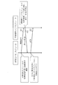
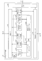
- FIG. 15 is a configuration diagram of the V storage destination management unit 13.
- the V storage location management unit 13 includes an input I / F 131, a communication I / F 132, a volatile memory I / F 133, and a path determination unit 134.
- the input I / F 131 is an interface for receiving data input from the external input bus 15.
- the communication I / F 132 is an interface for communicating with the NV storage destination management unit 14 via the inter-memory module bus 16.
- the volatile memory I / F 133 is an interface for transmitting and receiving data to and from the volatile memory chip 111.
- the route determination unit 134 is a function for executing the above-described survival confirmation processing and route determination processing.
- the route determination unit 134 includes a redundant memory activation unit 1341, a survival confirmation packet transmission unit 1342, a survival confirmation packet reception unit 1343, a connection request unit 1344, a connection permission confirmation unit 1345, a nonvolatile memory management table 1346, A timeout counter 1347.
- the redundant memory activation unit 1341 has a function of activating the nonvolatile memory module 12 in a standby state when a failure occurs in the nonvolatile memory module 12.
- the survival confirmation packet transmitting unit 1342, the survival confirmation packet receiving unit 1343, and the timeout counter 1347 are functions for executing the survival confirmation process.
- the connection request unit 1344, the connection permission confirmation unit 1345, and the nonvolatile memory management table 1346 are functions for executing a route determination process.
- the input I / F 131 transmits a survival confirmation processing start signal to the survival confirmation packet transmission unit 1342. At the same time, the input I / F 131 transmits data to the volatile memory I / F 133. When data is transmitted from the input I / F 131, the volatile memory I / F 133 writes the transmitted data to the volatile memory chip 111.
- the survival confirmation packet transmission unit 1342 When receiving the survival confirmation processing start signal from the input I / F 131, the survival confirmation packet transmission unit 1342 transmits a HELLO packet transmission signal to the communication I / F 132.
- the existence confirmation packet transmission unit 1342 transmits a count start signal to the timeout counter 1347 at the same time.
- the communication I / F 132 transmits the HELLO packet to all the connected nonvolatile memory modules 12.
- the timeout counter 1347 starts counting when it receives the count start signal.
- the time-out counter 1347 has the same number of counters as the connected non-volatile memory modules 12 and can count time for each connected non-volatile memory module 12.
- the communication I / F 132 When the communication I / F 132 receives the HELLO response packet from the nonvolatile memory module 12, the communication I / F 132 transmits a survival confirmation signal to the survival confirmation packet receiving unit 1343.
- the survival confirmation packet receiving unit 1343 transmits a count stop signal to the timeout counter 1347.
- the timeout counter 1347 stops the corresponding counter. The timeout counter 1347 simultaneously updates the failure information of the nonvolatile memory module 12 corresponding to the count stop signal in the nonvolatile memory management table 1346 to operation.
- the timeout counter 1347 sets a timeout when the counted value exceeds a predetermined value. When a timeout occurs, the timeout counter 1347 updates the failure information of the time-out nonvolatile memory module 12 in the nonvolatile memory management table 1346 to a failure. Further, the timeout counter 1347 transmits a redundant memory activation signal to the redundant memory activation unit 1341 when a timeout occurs. When the redundant memory activation unit 1341 receives the redundant memory activation signal, the redundant memory activation unit 1341 transmits a WAKEUP packet transmission signal to the communication I / F 132. When the communication I / F 132 receives the WAKEUP packet transmission signal, the communication I / F 132 transmits the WAKEUP packet to the non-volatile memory module 12 in the standby state.
- the timeout counter 1347 transmits a survival confirmation process completion signal to the connection request unit 1344 when all the counters are stopped.
- the communication I / F 132 transmits a HELLO packet reception signal to the survival confirmation packet receiving unit 1343.
- the survival confirmation packet receiving unit 1343 transmits a HELLO response packet generation signal to the survival confirmation packet transmitting unit 1342.
- the survival confirmation packet transmission unit 1342 transmits a HELLO response packet transmission signal to the communication I / F 132.
- the communication I / F 132 transmits the HELLO response packet to all the connected nonvolatile memory modules 12.
- connection request unit 1344 When the connection request unit 1344 receives the survival confirmation processing completion signal from the timeout counter 1347, the connection request unit 1344 updates all the connection requests in the nonvolatile memory management table 1346. From the nonvolatile memory management table 1346, the connection request unit 1344 selects the nonvolatile memory module 12 in which the failure information is active, the connection request has not been made, and the value of the nonvolatile memory module number is the smallest. A connection request packet transmission signal as a transmission destination is transmitted to the communication I / F 132. When the communication I / F 132 receives the connection request packet transmission signal from the connection request unit 1344, the communication I / F 132 transmits the connection request packet to the transmission destination nonvolatile memory module 12.
- connection permission confirmation unit 1345 When the communication I / F 132 receives the connection response packet from the inter-memory module bus 16, the communication I / F 132 transmits a connection response signal to the connection permission confirmation unit 1345.
- the connection permission confirmation unit 1345 Upon receiving a connection response signal from the communication I / F 132, the connection permission confirmation unit 1345 performs an operation according to the content of the signal.
- the connection permission confirmation unit 1345 transmits a write valid signal to the volatile memory I / F 133 when the connection is permitted.
- the connection permission confirmation unit 1345 transmits a re-request signal to the connection request unit 1344 when the connection is rejected.
- the connection permission confirmation unit 1345 updates the connection request for the corresponding nonvolatile memory module 12 in the nonvolatile memory management table 1346 to be completed.
- connection request unit 1344 When the connection request unit 1344 receives the re-request signal, the failure information is activated from the nonvolatile memory management table 1346, the connection request has not been made, and the value of the nonvolatile memory module number is the highest. A connection request is generated to the small nonvolatile memory module 12.
- the volatile memory I / F 133 reads data from the volatile memory chip 111 and transmits the data to the communication I / F 132 while receiving the write valid signal from the connection permission confirmation unit 1345.
- the communication I / F 132 receives data from the volatile memory I / F 211, the communication I / F 132 transmits the data to the nonvolatile memory module 12 via the inter-memory module bus 16.
- FIG. 16 is a configuration diagram of the NV storage destination management unit 14.
- the NV storage destination management unit 14 includes an output I / F 141, a communication I / F 142, a nonvolatile memory I / F 143, a path determination unit 144, and a write data transfer unit 145.
- the output I / F 141 is an interface for outputting data from the external output bus 17.
- the communication I / F 142 is an interface for communicating with the V storage destination management unit 13 via the inter-memory module bus 16.
- the nonvolatile memory I / F 143 is an interface for transmitting and receiving data to and from the nonvolatile memory chip 121.
- the route determination unit 144 is a function for executing the above-described survival confirmation processing and route determination processing.
- the write data transfer unit 145 is a function for controlling the writing of data transmitted from the volatile memory module 11 to the nonvolatile memory chip 121.
- the route determination unit 144 includes a redundant memory activation unit 1441, a survival confirmation packet transmission unit 1442, a survival confirmation packet reception unit 1443, a connection request response unit 1444, a connection permission determination unit 1445, and a volatile memory management table 1446. And a timeout counter 1447.
- the redundant memory activation unit 1441 is a function for activating the standby volatile memory module 11 when a failure occurs in the volatile memory module 11.
- a survival confirmation packet transmission unit 1442, a survival confirmation packet reception unit 1443, and a timeout counter 1447 are functions for executing a survival confirmation process.
- the connection request response unit 1444, the connection permission determination unit 1445, and the volatile memory management table 1446 are functions for executing a route determination process.
- the communication I / F 142 transmits a HELLO packet reception signal to the survival confirmation packet receiving unit 1443.
- the survival confirmation packet receiving unit 1443 transmits a HELLO response packet generation signal and a survival confirmation processing start signal to the survival confirmation packet transmitting unit 1442.
- the survival confirmation packet transmission unit 1442 transmits the HELLO response packet transmission signal to the communication I / F 142.
- the communication I / F 142 When the communication I / F 142 receives the HELLO response packet transmission signal, the communication I / F 142 transmits the HELLO response packet to all the connected volatile memory modules 11.
- the survival confirmation packet transmission unit 1442 receives a survival confirmation processing start signal from the survival confirmation packet reception unit 1443, the survival confirmation packet transmission unit 1442 transmits a HELLO packet transmission signal to the communication I / F 142.
- the survival confirmation packet transmission unit 1442 transmits a count start signal to the timeout counter 1447 at the same time.
- the communication I / F 142 receives the HELLO packet transmission signal
- the communication I / F 142 transmits the HELLO packet to all the connected volatile memory modules 11.
- the timeout counter 1447 starts counting when it receives the count start signal.
- the timeout counter 1447 has the same number of counters as the connected volatile memory modules 11, and can count the time for each connected volatile memory module 11.
- the communication I / F 142 transmits a survival confirmation signal to the survival confirmation packet receiving unit 1443.
- the survival confirmation packet receiving unit 1443 transmits a count stop signal to the timeout counter 1447.
- the timeout counter 1447 stops the corresponding counter.
- the timeout counter 1447 updates the failure information of the volatile memory module 11 corresponding to the count stop signal in the volatile memory management table 1446 to the operation.
- the timeout counter 1447 sets a timeout when the value being counted exceeds a predetermined value. When a timeout occurs, the timeout counter 1447 updates the failure information of the volatile memory module 11 that has timed out in the volatile memory management table 1446 to a failure. Further, the timeout counter 1447 transmits a redundant memory activation signal to the redundant memory activation unit 1441 when a timeout occurs. When the redundant memory activation unit 1441 receives the redundant memory activation signal, the redundant memory activation unit 1441 transmits a WAKEUP packet transmission signal to the communication I / F 142. When the communication I / F 142 receives the WAKEUP packet transmission signal, the communication I / F 142 transmits the WAKEUP packet to the volatile memory module 11 in the standby state.
- the communication I / F 142 When the communication I / F 142 receives the connection request packet from the inter-memory module bus 16, the communication I / F 142 transmits a connection request reception signal to the connection permission determination unit 1445.
- the connection permission determination unit 1445 Upon receiving the connection request reception signal from the communication I / F 142, the connection permission determination unit 1445 sets the number of paths of the volatile memory module 11 that is the transmission source of the connection request packet in the volatile memory management table 1446 to the number of paths of the connection request packet. Update.
- the connection permission determination unit 1445 determines that the volatile memory module 11 that is the transmission source of the connection request packet has the smallest number of paths and the smallest volatile memory module number in the volatile memory management table 1446. Check if it is.
- connection permission judgment unit 1445 transmits a connection permission signal to the connection request response unit 1444, and otherwise. Transmits a connection rejection signal to the connection request response unit 1444.
- the connection request response unit 1444 receives the connection permission signal from the connection permission determination unit 1445, the connection request response unit 1444 transmits a connection response packet transmission signal designating connection permission to the communication I / F 142.
- the connection request response unit 1444 receives the connection rejection signal from the connection permission determination unit 1445, the connection request response unit 1444 transmits a connection response packet transmission signal designating connection rejection to the communication I / F 142.
- the communication I / F 142 Upon receiving the connection response packet transmission signal from the connection request response unit 1444, the communication I / F 142 transmits the connection response packet to the volatile memory I / F 2 that is the transmission source of the connection request packet. If the connection permission determination unit 1445 has already transmitted a connection permission signal and then received a connection request reception signal that should be prioritized, the connection permission determination unit 1445 sends a connection rejection signal to the volatile memory module 11 that once transmitted the connection permission signal. It transmits to the connection request response part 1444. Then, the connection permission determination unit 1445 transmits a connection permission signal for the volatile memory module 11 that is the transmission source of the connection request packet to the connection request response unit 1444.
- the connection permission determination unit 1445 When transmitting a connection permission signal, the connection permission determination unit 1445 asserts a write valid signal to the write data transfer unit 145.
- the communication I / F 142 transfers the data to the write data transfer unit 145.
- the write data transfer unit 145 transfers data transferred from the communication I / F 142 to the nonvolatile memory I / F 122 while the write enable signal is asserted from the connection permission determination unit 1445.
- the write data transfer unit 145 discards the data transferred from the communication I / F 142 while the write enable signal is deasserted from the connection permission determination unit 1445.
- the nonvolatile memory I / F 122 writes data to the nonvolatile memory chip 121 when data is transferred from the write data transfer unit 145.
- the output I / F 141 When the output I / F 141 receives a data read request from the external output bus 17, the output I / F 141 transmits the read request to the nonvolatile memory I / F 122.
- the nonvolatile memory I / F 122 receives a read request from the output I / F 141, the nonvolatile memory I / F 122 reads data from the nonvolatile memory chip 121 and transmits the data to the output I / F 141.
- the output I / F 141 When receiving data from the nonvolatile memory I / F 122, the output I / F 141 transmits the data to the external output bus 17.
- each volatile memory module 11 and each nonvolatile memory module 12 autonomously determines a data transfer path by a 3WAY handshake. Therefore, it is not necessary to use a mechanism for managing and controlling information such as a data storage destination in a unified manner and a crossbar switch circuit. As a result, the entire memory system 10 does not become inoperable when a mechanism for managing and controlling information such as a data storage destination or a crossbar switch circuit fails.
- the volatile memory module 11 in the non-volatile memory module 12 is activated.
- the nonvolatile memory module 12 in the standby state is activated. Therefore, it is possible to prevent a decrease in performance when some volatile memory modules 11 and some nonvolatile memory modules 12 fail.
- the volatile memory module 11 and the non-volatile memory module 12 existing more than necessary can be set in a standby state, and unnecessary power consumption can be reduced.
- all transmission units described as “ ⁇ packet” include a “packet type” field for indicating a packet type.
- Each storage destination management unit determines the type of packet from the “packet type” field.
- the function described as “unit” may be realized by software, or may be realized by a circuit or a device.
- the software that realizes the function described as “ ⁇ unit” is a storage device (for example, nonvolatile memory module 12) in the memory system 10. And is read and executed by an arithmetic device (CPU or the like) included in the memory system 10.
Abstract
Description
揮発性メモリモジュール及び不揮発性メモリモジュールに故障が発生すると、メモリシステムへの書込み速度が低下してしまうことやシステムが停止してしまうことがある。
しかし、データ保存先等の情報を一元に管理・制御する機構、又は、クロスバースイッチ回路が故障した場合、メモリシステム全体が動作しなくなってしまう。
データを一時記憶する複数の第1メモリモジュールと、
各第1メモリモジュールに設けられた第1保存先管理部と、
各第1メモリモジュールに記憶されたデータを記憶する複数の第2メモリモジュールと、
各第2メモリモジュールに設けられた第2保存先管理部と
を備え、
前記各第1メモリモジュールに設けられた前記第1保存先管理部と、前記各第2メモリモジュールに設けられた前記第2保存先管理部とが通信して、データを記憶した第1メモリモジュール毎に、データの送信先の第2メモリモジュールを決定し、
前記各第1メモリモジュールが、決定した送信先の第2メモリモジュールへデータを送信する
ことを特徴とする。
図1は、実施の形態1に係るメモリシステム10(データ記憶装置)の構成図である。
メモリシステム10は、複数の揮発性メモリモジュール11(第1メモリモジュール)と、複数の不揮発性メモリモジュール12(第2メモリモジュール)とを備える。各揮発性メモリモジュール11は、V保存先管理部13(第1保存先管理部)を備える。各不揮発性メモリモジュール12は、NV保存先管理部14(第2保存先管理部)を備える。
各揮発性メモリモジュール11は、例えば、DRAM(Dynamic Random Access Memory)モジュールであり、各不揮発性メモリモジュール12は、例えば、フラッシュメモリモジュールである。
各揮発性メモリモジュール11と各不揮発性メモリモジュール12とは、メモリモジュール間バス16で接続されている。各揮発性メモリモジュール11及び各不揮発性メモリモジュール12のポート数には限りがあるため、全ての揮発性メモリモジュール11と全ての不揮発性メモリモジュール12とが接続されているわけではない。
各不揮発性メモリモジュール12は、外部出力バス17が接続されている。各不揮発性メモリモジュール12は、メモリモジュール間バス16を介して揮発性メモリモジュール11から送信されたデータを記憶する。各不揮発性メモリモジュール12は、外部出力バス17を介して、記憶したデータを出力する。
不揮発性メモリ管理テーブル1346は、不揮発性メモリモジュール番号、故障情報、接続要求を有している。
不揮発性メモリモジュール番号は、不揮発性メモリモジュール12の識別子である。図1では、不揮発性メモリモジュール12は、1番~n番までのn個あり、この番号が不揮発性メモリモジュール番号である。故障情報は、不揮発性メモリモジュール12が故障しているか否かを示す情報である。接続要求は、不揮発性メモリモジュール12へ接続要求を出したか否かを示す情報である。
揮発性メモリ管理テーブル1446は、揮発性メモリモジュール番号、故障情報、パス数、使用権付与を有している。
揮発性メモリモジュール番号は、揮発性メモリモジュール11の識別子である。図1では、揮発性メモリモジュール11は、1番~m番までのm個あり、この番号が揮発性メモリモジュール番号である。故障情報は、揮発性メモリモジュール11が故障しているか否かを示す情報である。パス数は、揮発性メモリモジュール11に接続されている、故障していない不揮発性メモリモジュール12の数である。使用権付与は、接続要求に対して許可しているか否かを示す情報である。
(S1:データ入力処理)
メモリシステム10へデータが入力される。すると、外部入力バス15を介して各揮発性メモリモジュール11へデータが入力され、各揮発性メモリモジュール11にデータが分散して記憶される。
各揮発性メモリモジュール11のV保存先管理部13は、不揮発性メモリモジュール12の故障情報を収集する。
揮発性メモリモジュール11のV保存先管理部13は、接続されている全ての不揮発性メモリモジュール12のNV保存先管理部14に対してHELLOパケット(生存確認メッセージ)を送信する(1)。HELLOパケットを受信した不揮発性メモリモジュール12のNV保存先管理部14は、揮発性メモリモジュール11のV保存先管理部13に対してHELLO応答パケットを送信する(2)。
揮発性メモリモジュール11のV保存先管理部13は、送信したHELLOパケットに対してHELLO応答パケットの送信があった不揮発性メモリモジュール12は動作している(故障していない)として扱う。一方、揮発性メモリモジュール11のV保存先管理部13は、所定時間内に送信がなかった不揮発性メモリモジュール12は動作していない(故障している)として扱う。そして、揮発性メモリモジュール11のV保存先管理部13は、不揮発性メモリ管理テーブル1346の故障情報を更新する。
不揮発性メモリモジュール12のNV保存先管理部14は、揮発性メモリモジュール11の故障情報を収集する。
不揮発性メモリモジュール12のNV保存先管理部14は、接続されている全ての揮発性メモリモジュール11のV保存先管理部13に対してHELLOパケットを送信する(1)。HELLOパケットを受信した揮発性メモリモジュール11のV保存先管理部13は、不揮発性メモリモジュール12のNV保存先管理部14に対してHELLO応答パケットを送信する(2)。
不揮発性メモリモジュール12のNV保存先管理部14は、送信したHELLOパケットに対してHELLO応答パケットの送信があった揮発性メモリモジュール11は動作している(故障していない)として扱う。一方、不揮発性メモリモジュール12のNV保存先管理部14は、所定時間内に送信がなかった揮発性メモリモジュール11は動作していない(故障している)として扱う。そして、不揮発性メモリモジュール12のNV保存先管理部14は、揮発性メモリ管理テーブル1446の故障情報を更新する。
HELLOパケットは、送信先のメモリモジュール番号、送信元のメモリモジュール番号を有している。
揮発性メモリモジュール11のV保存先管理部13がHELLOパケットを送信する場合には、送信先のメモリモジュール番号は送信先の不揮発性メモリモジュール12の不揮発性メモリモジュール番号となり、送信元のメモリモジュール番号は送信元の揮発性メモリモジュール11の揮発性メモリモジュール番号となる。一方、不揮発性メモリモジュール12のNV保存先管理部14がHELLOパケットを送信する場合には、送信先のメモリモジュール番号は送信先の揮発性メモリモジュール11の揮発性メモリモジュール番号となり、送信元のメモリモジュール番号は送信元の不揮発性メモリモジュール12の不揮発性メモリモジュール番号となる。
HELLO応答パケットは、送信先のメモリモジュール番号、送信元のメモリモジュール番号を有している。
HELLO応答パケットの送信先のメモリモジュール番号及び送信元のメモリモジュール番号は、HELLOパケットの場合と同じであるため説明を省略する。
同様に、生存確認処理で、揮発性メモリモジュール11の故障が検出された場合は、不揮発性メモリモジュール12のNV保存先管理部14は、WAKEUPパケットを待機状態になっている揮発性メモリモジュール11へ送信する。待機状態になっている揮発性メモリモジュール11は、WAKEUPパケットを受信すると、稼働状態になり、HELLOパケット及びHELLO応答パケットを送信するようになる。
揮発性メモリモジュール11のV保存先管理部13と、不揮発性メモリモジュール12のNV保存先管理部14とは、不揮発性メモリ管理テーブル1346の故障情報と、揮発性メモリ管理テーブル1446の故障情報及びパス数とを用いて、データ転送経路を決定する。
揮発性メモリモジュール11のV保存先管理部13は、不揮発性メモリ管理テーブル1346の故障情報が故障していないことを示す不揮発性メモリモジュール12に対して順に接続要求パケット(接続要求メッセージ)を送信する。例えば、揮発性メモリモジュール11のV保存先管理部13は、不揮発性メモリモジュール番号の昇順に接続要求パケットを送信する。
この際、揮発性メモリモジュール11のV保存先管理部13は、不揮発性メモリ管理テーブル1346の故障情報が故障していないことを示す不揮発性メモリモジュール12の数をパス数としてカウントする。そして、揮発性メモリモジュール11のV保存先管理部13は、パス数を接続要求パケットに含めて送信する。
不揮発性メモリモジュール12のNV保存先管理部14は、受信した接続要求パケットのうち、パス数が最も少ない接続要求パケットに対して、許可を示す接続応答パケット(接続了承メッセージ)を送信し、その他の接続要求パケットに対して、拒否を示す接続応答パケットを送信する。
なお、最も少ないパス数を持つ接続要求パケットが同率で存在する場合がある。この場合、不揮発性メモリモジュール12のNV保存先管理部14は、送信元の揮発性メモリモジュール11の揮発性メモリモジュール番号が最も小さい接続要求パケットに対して、許可を示す接続応答パケットを送信する。
不揮発性メモリモジュール12のNV保存先管理部14は、受信した接続要求パケットに含まれるパス数により、揮発性メモリ管理テーブル1446のパス数を更新する。また、不揮発性メモリモジュール12のNV保存先管理部14は、送信した接続応答パケットに応じて、揮発性メモリ管理テーブル1446の使用権付与を更新する。
揮発性メモリモジュール11のV保存先管理部13は、接続応答パケットを受信した場合、接続応答パケットの送信元の不揮発性メモリモジュール12について、不揮発性メモリ管理テーブル1346の接続要求を済に更新する。
この場合、拒否を示す接続応答パケットを受信した揮発性メモリモジュール11のV保存先管理部13は、一旦中止していた接続要求パケットの送信を再開する。
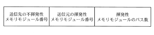
接続要求パケットは、送信先の不揮発性メモリモジュール番号、送信元の揮発性メモリモジュール番号、揮発性メモリモジュールのパス数を有している。
送信先の不揮発性メモリモジュール番号は、送信先の不揮発性メモリモジュール12の不揮発性メモリモジュール番号である。送信元の揮発性メモリモジュール番号は、送信元の揮発性メモリモジュール11の揮発性メモリモジュール番号である。揮発性メモリモジュールのパス数は、送信元の揮発性メモリモジュール11のパス数である。
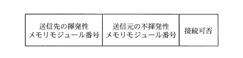
接続応答パケットは、送信先の揮発性メモリモジュール番号、送信元の不揮発性メモリモジュール番号、接続可否を有している。
送信先の揮発性メモリモジュール番号は、送信先の揮発性メモリモジュール11の揮発性メモリモジュール番号である。送信元の不揮発性メモリモジュール番号は、送信元の不揮発性メモリモジュール12の不揮発性メモリモジュール番号である。接続可否は、許可又は拒否を示す情報である。
不揮発性メモリ管理テーブル1346の故障情報が動作となっており、かつ、接続要求が未となっている不揮発性メモリモジュール12が接続要求パケットの送信先として選択される。接続要求パケットの揮発性メモリモジュールのパス数は、不揮発性メモリ管理テーブル1346の故障情報が動作となっている不揮発性メモリモジュール12の数である。
揮発性メモリ管理テーブル1446のパス数は、接続要求パケットの揮発性メモリモジュールのパス数が設定される。設定されたパス数に基づき、使用権付与を有(許可)にするか、無(拒否)にするかが決定される。決定された使用権付与が、接続応答パケットの接続可否に反映される。
そして、接続応答パケットの送信元の不揮発性メモリモジュール12について、不揮発性メモリ管理テーブル1346の接続要求が済に更新される。
各揮発性メモリモジュール11のV保存先管理部13は、S4で受信した許可を示す接続応答パケットの送信元の不揮発性メモリモジュール12に対して、S1で一時記憶したデータを転送する。ここで、各揮発性メモリモジュール11は、並列にデータを転送することが可能である。
揮発性メモリモジュール11は、V保存先管理部13と、1つ又は複数の揮発性メモリチップ111とを備える。V保存先管理部13と各揮発性メモリチップ111とは、揮発性メモリ用バス112で接続されている。
不揮発性メモリモジュール12は、NV保存先管理部14と、1つ又は複数の不揮発性メモリチップ121とを備える。NV保存先管理部14と各不揮発性メモリチップ121とは、不揮発性メモリ用バス122で接続されている。
V保存先管理部13は、入力I/F131と、通信I/F132と、揮発性メモリI/F133と、経路決定部134とを備える。
タイムアウト用カウンタ1347は、カウント開始信号を受信すると、カウントを開始する。タイムアウト用カウンタ1347は、接続されている不揮発性メモリモジュール12と同じ数だけカウンタを有しており、接続されている不揮発性メモリモジュール12毎に時間をカウントすることが可能である。
通信I/F132は、不揮発性メモリモジュール12からHELLO応答パケットを受信すると、生存確認信号を生存確認パケット受信部1343へ送信する。生存確認パケット受信部1343は、通信I/F132から生存確認信号を受信すると、カウント停止信号をタイムアウト用カウンタ1347へ送信する。タイムアウト用カウンタ1347は、生存確認パケット受信部1343から、カウント停止信号を受信すると、対応するカウンタを停止する。タイムアウト用カウンタ1347は、同時に、不揮発性メモリ管理テーブル1346における、カウント停止信号に対応する不揮発性メモリモジュール12の故障情報を動作に更新する。
冗長メモリ起動部1341は、冗長メモリ起動信号を受信すると、WAKEUPパケット送信信号を通信I/F132へ送信する。通信I/F132は、WAKEUPパケット送信信号を受信すると、待機状態になっている不揮発性メモリモジュール12へWAKEUPパケットを送信する。
生存確認パケット送信部1342は、生存確認パケット受信部1343からHELLO応答パケット生成信号を受信すると、HELLO応答パケット送信信号を通信I/F132へ送信する。通信I/F132は、HELLO応答パケット送信信号を受信すると、接続されている全ての不揮発性メモリモジュール12へHELLO応答パケットを送信する。
接続要求部1344は、不揮発性メモリ管理テーブル1346から、故障情報が動作になっており、かつ、接続要求が未であり、かつ、不揮発性メモリモジュール番号の値が最も小さい不揮発性メモリモジュール12を送信先とする接続要求パケット送信信号を通信I/F132へ送信する。通信I/F132は、接続要求部1344から接続要求パケット送信信号を受信すると、送信先の不揮発性メモリモジュール12へ接続要求パケットを送信する。
NV保存先管理部14は、出力I/F141と、通信I/F142と、不揮発性メモリI/F143と、経路決定部144と、書込みデータ転送部145とを備える。
生存確認パケット送信部1442は、生存確認パケット受信部1443からHELLO応答パケット生成信号を受信すると、HELLO応答パケット送信信号を通信I/F142へ送信する。通信I/F142は、HELLO応答パケット送信信号を受信すると、接続されている全ての揮発性メモリモジュール11へHELLO応答パケットを送信する。
また、生存確認パケット送信部1442は、生存確認パケット受信部1443から、生存確認処理開始信号を受信すると、HELLOパケット送信信号を通信I/F142へ送信する。生存確認パケット送信部1442は、同時にカウント開始信号をタイムアウト用カウンタ1447へ送信する。通信I/F142は、HELLOパケット送信信号を受信すると、接続されている全ての揮発性メモリモジュール11へHELLOパケットを送信する。
タイムアウト用カウンタ1447は、カウント開始信号を受信すると、カウントを開始する。タイムアウト用カウンタ1447は、接続されている揮発性メモリモジュール11と同じ数だけカウンタを有しており、接続されている揮発性メモリモジュール11毎に時間をカウントすることが可能である。
通信I/F142は、揮発性メモリモジュール11からHELLO応答パケットを受信すると、生存確認信号を生存確認パケット受信部1443へ送信する。生存確認パケット受信部1443は、通信I/F142から生存確認信号を受信すると、カウント停止信号をタイムアウト用カウンタ1447へ送信する。タイムアウト用カウンタ1447は、生存確認パケット受信部1443から、カウント停止信号を受信すると、対応するカウンタを停止する。タイムアウト用カウンタ1447は、同時に、揮発性メモリ管理テーブル1446における、カウント停止信号に対応する揮発性メモリモジュール11の故障情報を動作に更新する。
冗長メモリ起動部1441は、冗長メモリ起動信号を受信すると、WAKEUPパケット送信信号を通信I/F142へ送信する。通信I/F142は、WAKEUPパケット送信信号を受信すると、待機状態になっている揮発性メモリモジュール11へWAKEUPパケットを送信する。
接続要求応答部1444は、接続許可判断部1445から接続許可信号を受信すると、接続許可を指定した接続応答パケット送信信号を通信I/F142へ送信する。一方、接続要求応答部1444は、接続許可判断部1445から接続拒否信号を受信すると、接続拒否を指定した接続応答パケット送信信号を通信I/F142へ送信する。通信I/F142は、接続要求応答部1444から接続応答パケット送信信号を受信すると、接続応答パケットを接続要求パケットの送信元の揮発性メモリI/F2へ送信する。
なお、接続許可判断部1445は、既に接続許可信号を送信した後に、更に優先するべき接続要求受信信号を受信した場合には、一旦接続許可信号を送信した揮発性メモリモジュール11に対する接続拒否信号を接続要求応答部1444へ送信する。その上で、接続許可判断部1445は、接続要求パケットの送信元の揮発性メモリモジュール11に対する接続許可信号を接続要求応答部1444へ送信する。
不揮発性メモリI/F122は、書込みデータ転送部145からデータが転送された場合、不揮発性メモリチップ121にデータをライトする。
そのため、一部の揮発性メモリモジュール11や一部の不揮発性メモリモジュール12が故障した場合における性能の低下を防止することができる。また、必要以上に存在する揮発性メモリモジュール11や不揮発性メモリモジュール12を待機状態とすることができ、不要な電力消費を減らすことができる。
Claims (6)
- データを一時記憶する複数の第1メモリモジュールと、
各第1メモリモジュールに設けられた第1保存先管理部と、
各第1メモリモジュールに記憶されたデータを記憶する複数の第2メモリモジュールと、
各第2メモリモジュールに設けられた第2保存先管理部と
を備え、
前記各第1メモリモジュールに設けられた前記第1保存先管理部と、前記各第2メモリモジュールに設けられた前記第2保存先管理部とが通信して、データを記憶した第1メモリモジュール毎に、データの送信先の第2メモリモジュールを決定し、
前記各第1メモリモジュールが、決定した送信先の第2メモリモジュールへデータを送信する
ことを特徴とするデータ記憶装置。 - 前記第1保存先管理部は、前記各第2メモリモジュールへ生存確認メッセージを送信し、送信先の第2メモリモジュールが決定するまで、前記生存確認メッセージに対して応答があった第2メモリモジュールへ順に、送信先の第2メモリモジュールになることを依頼する接続要求メッセージを送信し、
前記第2保存先管理部は、前記生存確認メッセージに対する応答の受信数に応じて決定した第1保存先管理部へ、前記送信先の第2メモリモジュールになることを了承する接続了承メッセージを送信する
ことを特徴とする請求項1に記載のデータ記憶装置。 - 前記第1保存先管理部は、前記受信数を含む前記接続要求メッセージを送信する
ことを特徴とする請求項2に記載のデータ記憶装置。 - 前記第2保存先管理部は、前記受信数が少ない第1保存先管理部に前記接続了承メッセージを送信し、既に前記接続了承メッセージを送信した前記第1保存先管理部がある場合において、前記受信数がより少ない前記第1保存先管理部から前記接続要求メッセージを受信した場合には、前記受信数がより少ない前記第1保存先管理部へ前記接続了承メッセージを送信するとともに、既に前記接続了承メッセージを送信した前記第1保存先管理部へ前記送信先の第2メモリモジュールになることを撤回する接続撤回メッセージを送信し、
前記第1保存先管理部は、前記接続撤回メッセージを受信すると、前記接続要求メッセージの送信を再開する
ことを特徴とする請求項2又は3に記載のデータ記憶装置。 - 前記第2メモリモジュールは、バックアップ用に待機状態になっているものが含まれており、
前記第1保存先管理部は、前記生存確認メッセージに対して応答がない第2メモリモジュールがある場合には、前記待機状態になっている第2メモリモジュールへ起動メッセージを送信して、前記待機状態になっている第2メモリモジュールを稼働させる
ことを特徴とする請求項2から4までのいずれかに記載のデータ記憶装置。 - 前記第1メモリモジュールは、バックアップ用に待機状態になっているものが含まれており、
前記第2保存先管理部は、前記各第1メモリモジュールへ生存確認メッセージを送信し、前記生存確認メッセージに対して応答がない第1メモリモジュールがある場合には、前記待機状態になっている第1メモリモジュールへ起動メッセージを送信して、前記待機状態になっている第1メモリモジュールを稼働させる
ことを特徴とする請求項2から5までのいずれかに記載のデータ記憶装置。
Priority Applications (4)
| Application Number | Priority Date | Filing Date | Title |
|---|---|---|---|
| US15/121,136 US10372361B2 (en) | 2014-02-27 | 2014-02-27 | Data storage device including multiple memory modules and circuitry to manage communication among the multiple memory modules |
| JP2016504921A JP6141511B2 (ja) | 2014-02-27 | 2014-02-27 | データ記憶装置 |
| EP14883990.5A EP3113027A4 (en) | 2014-02-27 | 2014-02-27 | Data storage device |
| PCT/JP2014/054792 WO2015128976A1 (ja) | 2014-02-27 | 2014-02-27 | データ記憶装置 |
Applications Claiming Priority (1)
| Application Number | Priority Date | Filing Date | Title |
|---|---|---|---|
| PCT/JP2014/054792 WO2015128976A1 (ja) | 2014-02-27 | 2014-02-27 | データ記憶装置 |
Publications (1)
| Publication Number | Publication Date |
|---|---|
| WO2015128976A1 true WO2015128976A1 (ja) | 2015-09-03 |
Family
ID=54008345
Family Applications (1)
| Application Number | Title | Priority Date | Filing Date |
|---|---|---|---|
| PCT/JP2014/054792 WO2015128976A1 (ja) | 2014-02-27 | 2014-02-27 | データ記憶装置 |
Country Status (4)
| Country | Link |
|---|---|
| US (1) | US10372361B2 (ja) |
| EP (1) | EP3113027A4 (ja) |
| JP (1) | JP6141511B2 (ja) |
| WO (1) | WO2015128976A1 (ja) |
Citations (5)
| Publication number | Priority date | Publication date | Assignee | Title |
|---|---|---|---|---|
| JPH05158797A (ja) * | 1991-12-06 | 1993-06-25 | Hitachi Ltd | 外部記憶サブシステム |
| JPH0720994A (ja) * | 1993-06-30 | 1995-01-24 | Hitachi Ltd | 記憶システム |
| JP2004192482A (ja) * | 2002-12-13 | 2004-07-08 | Hitachi Ltd | バックアップを特定するクラスタ型計算機システム及びクラスタ型ストレージシステム |
| JP2005043930A (ja) * | 2003-07-22 | 2005-02-17 | Hitachi Ltd | 記憶装置システム |
| JP2013532339A (ja) * | 2010-06-18 | 2013-08-15 | エルエスアイ コーポレーション | スケーラブルな記憶装置 |
Family Cites Families (12)
| Publication number | Priority date | Publication date | Assignee | Title |
|---|---|---|---|---|
| US5295258A (en) | 1989-12-22 | 1994-03-15 | Tandem Computers Incorporated | Fault-tolerant computer system with online recovery and reintegration of redundant components |
| US5317752A (en) | 1989-12-22 | 1994-05-31 | Tandem Computers Incorporated | Fault-tolerant computer system with auto-restart after power-fall |
| US5327553A (en) | 1989-12-22 | 1994-07-05 | Tandem Computers Incorporated | Fault-tolerant computer system with /CONFIG filesystem |
| DE69032508T2 (de) | 1989-12-22 | 1999-03-25 | Tandem Computers Inc | Fehlertolerantes Rechnersystem mit Online-Wiedereinfügung und Abschaltung/Start |
| US5603058A (en) | 1994-09-08 | 1997-02-11 | International Business Machines Corporation | Video optimized media streamer having communication nodes received digital data from storage node and transmitted said data to adapters for generating isochronous digital data streams |
| US5668948A (en) | 1994-09-08 | 1997-09-16 | International Business Machines Corporation | Media streamer with control node enabling same isochronous streams to appear simultaneously at output ports or different streams to appear simultaneously at output ports |
| US5761417A (en) | 1994-09-08 | 1998-06-02 | International Business Machines Corporation | Video data streamer having scheduler for scheduling read request for individual data buffers associated with output ports of communication node to one storage node |
| US5712976A (en) | 1994-09-08 | 1998-01-27 | International Business Machines Corporation | Video data streamer for simultaneously conveying same one or different ones of data blocks stored in storage node to each of plurality of communication nodes |
| JP2003162377A (ja) | 2001-11-28 | 2003-06-06 | Hitachi Ltd | ディスクアレイシステム及びコントローラ間での論理ユニットの引き継ぎ方法 |
| JP2007323103A (ja) | 2006-05-30 | 2007-12-13 | Fujitsu Ltd | オンボード電源を備えたボード及びボードのリセット制御方法 |
| JP4849637B2 (ja) | 2007-08-31 | 2012-01-11 | ルネサスエレクトロニクス株式会社 | メモリカード及びメモリコントローラ |
| WO2010137178A1 (en) | 2009-05-25 | 2010-12-02 | Hitachi,Ltd. | Storage subsystem |
-
2014
- 2014-02-27 EP EP14883990.5A patent/EP3113027A4/en not_active Withdrawn
- 2014-02-27 JP JP2016504921A patent/JP6141511B2/ja not_active Expired - Fee Related
- 2014-02-27 WO PCT/JP2014/054792 patent/WO2015128976A1/ja active Application Filing
- 2014-02-27 US US15/121,136 patent/US10372361B2/en not_active Expired - Fee Related
Patent Citations (5)
| Publication number | Priority date | Publication date | Assignee | Title |
|---|---|---|---|---|
| JPH05158797A (ja) * | 1991-12-06 | 1993-06-25 | Hitachi Ltd | 外部記憶サブシステム |
| JPH0720994A (ja) * | 1993-06-30 | 1995-01-24 | Hitachi Ltd | 記憶システム |
| JP2004192482A (ja) * | 2002-12-13 | 2004-07-08 | Hitachi Ltd | バックアップを特定するクラスタ型計算機システム及びクラスタ型ストレージシステム |
| JP2005043930A (ja) * | 2003-07-22 | 2005-02-17 | Hitachi Ltd | 記憶装置システム |
| JP2013532339A (ja) * | 2010-06-18 | 2013-08-15 | エルエスアイ コーポレーション | スケーラブルな記憶装置 |
Non-Patent Citations (1)
| Title |
|---|
| See also references of EP3113027A4 * |
Also Published As
| Publication number | Publication date |
|---|---|
| US10372361B2 (en) | 2019-08-06 |
| JPWO2015128976A1 (ja) | 2017-03-30 |
| EP3113027A4 (en) | 2017-11-01 |
| EP3113027A1 (en) | 2017-01-04 |
| US20170220286A1 (en) | 2017-08-03 |
| JP6141511B2 (ja) | 2017-06-07 |
Similar Documents
| Publication | Publication Date | Title |
|---|---|---|
| US10110499B2 (en) | QoS in a system with end-to-end flow control and QoS aware buffer allocation | |
| US11792132B2 (en) | Technologies for aligning network flows to processing resources | |
| US9009648B2 (en) | Automatic deadlock detection and avoidance in a system interconnect by capturing internal dependencies of IP cores using high level specification | |
| US9397851B2 (en) | Directed route load/store packets for distributed switch initialization | |
| JP2018125044A5 (ja) | ||
| US8204054B2 (en) | System having a plurality of nodes connected in multi-dimensional matrix, method of controlling system and apparatus | |
| US9007920B2 (en) | QoS in heterogeneous NoC by assigning weights to NoC node channels and using weighted arbitration at NoC nodes | |
| EP2605451B1 (en) | Node controller link switching method, processor system and node | |
| KR20160054007A (ko) | 메모리 모듈 액세스 방법 및 장치 | |
| US20230421451A1 (en) | Method and system for facilitating high availability in a multi-fabric system | |
| US20140372646A1 (en) | Receiver based communication permission token allocation | |
| JP6141511B2 (ja) | データ記憶装置 | |
| US8732331B2 (en) | Managing latencies in a multiprocessor interconnect | |
| CN104618121A (zh) | 交换器及服务器系统 | |
| US20230016684A1 (en) | Communications Method and Related Apparatus | |
| JP2017092750A (ja) | 集線装置及び方法 |
Legal Events
| Date | Code | Title | Description |
|---|---|---|---|
| 121 | Ep: the epo has been informed by wipo that ep was designated in this application |
Ref document number: 14883990 Country of ref document: EP Kind code of ref document: A1 |
|
| ENP | Entry into the national phase |
Ref document number: 2016504921 Country of ref document: JP Kind code of ref document: A |
|
| WWE | Wipo information: entry into national phase |
Ref document number: 15121136 Country of ref document: US |
|
| NENP | Non-entry into the national phase |
Ref country code: DE |
|
| REEP | Request for entry into the european phase |
Ref document number: 2014883990 Country of ref document: EP |
|
| WWE | Wipo information: entry into national phase |
Ref document number: 2014883990 Country of ref document: EP |