WO2015114970A1 - 液晶表示装置 - Google Patents
液晶表示装置 Download PDFInfo
- Publication number
- WO2015114970A1 WO2015114970A1 PCT/JP2014/083101 JP2014083101W WO2015114970A1 WO 2015114970 A1 WO2015114970 A1 WO 2015114970A1 JP 2014083101 W JP2014083101 W JP 2014083101W WO 2015114970 A1 WO2015114970 A1 WO 2015114970A1
- Authority
- WO
- WIPO (PCT)
- Prior art keywords
- pixel
- electrode
- voltage
- liquid crystal
- pair
- Prior art date
- Legal status (The legal status is an assumption and is not a legal conclusion. Google has not performed a legal analysis and makes no representation as to the accuracy of the status listed.)
- Ceased
Links
Images










Classifications
-
- G—PHYSICS
- G09—EDUCATION; CRYPTOGRAPHY; DISPLAY; ADVERTISING; SEALS
- G09G—ARRANGEMENTS OR CIRCUITS FOR CONTROL OF INDICATING DEVICES USING STATIC MEANS TO PRESENT VARIABLE INFORMATION
- G09G3/00—Control arrangements or circuits, of interest only in connection with visual indicators other than cathode-ray tubes
- G09G3/20—Control arrangements or circuits, of interest only in connection with visual indicators other than cathode-ray tubes for presentation of an assembly of a number of characters, e.g. a page, by composing the assembly by combination of individual elements arranged in a matrix no fixed position being assigned to or needed to be assigned to the individual characters or partial characters
- G09G3/2007—Display of intermediate tones
- G09G3/2018—Display of intermediate tones by time modulation using two or more time intervals
-
- G—PHYSICS
- G09—EDUCATION; CRYPTOGRAPHY; DISPLAY; ADVERTISING; SEALS
- G09G—ARRANGEMENTS OR CIRCUITS FOR CONTROL OF INDICATING DEVICES USING STATIC MEANS TO PRESENT VARIABLE INFORMATION
- G09G3/00—Control arrangements or circuits, of interest only in connection with visual indicators other than cathode-ray tubes
- G09G3/20—Control arrangements or circuits, of interest only in connection with visual indicators other than cathode-ray tubes for presentation of an assembly of a number of characters, e.g. a page, by composing the assembly by combination of individual elements arranged in a matrix no fixed position being assigned to or needed to be assigned to the individual characters or partial characters
- G09G3/34—Control arrangements or circuits, of interest only in connection with visual indicators other than cathode-ray tubes for presentation of an assembly of a number of characters, e.g. a page, by composing the assembly by combination of individual elements arranged in a matrix no fixed position being assigned to or needed to be assigned to the individual characters or partial characters by control of light from an independent source
- G09G3/36—Control arrangements or circuits, of interest only in connection with visual indicators other than cathode-ray tubes for presentation of an assembly of a number of characters, e.g. a page, by composing the assembly by combination of individual elements arranged in a matrix no fixed position being assigned to or needed to be assigned to the individual characters or partial characters by control of light from an independent source using liquid crystals
- G09G3/3607—Control arrangements or circuits, of interest only in connection with visual indicators other than cathode-ray tubes for presentation of an assembly of a number of characters, e.g. a page, by composing the assembly by combination of individual elements arranged in a matrix no fixed position being assigned to or needed to be assigned to the individual characters or partial characters by control of light from an independent source using liquid crystals for displaying colours or for displaying grey scales with a specific pixel layout, e.g. using sub-pixels
-
- G—PHYSICS
- G02—OPTICS
- G02F—OPTICAL DEVICES OR ARRANGEMENTS FOR THE CONTROL OF LIGHT BY MODIFICATION OF THE OPTICAL PROPERTIES OF THE MEDIA OF THE ELEMENTS INVOLVED THEREIN; NON-LINEAR OPTICS; FREQUENCY-CHANGING OF LIGHT; OPTICAL LOGIC ELEMENTS; OPTICAL ANALOGUE/DIGITAL CONVERTERS
- G02F1/00—Devices or arrangements for the control of the intensity, colour, phase, polarisation or direction of light arriving from an independent light source, e.g. switching, gating or modulating; Non-linear optics
- G02F1/01—Devices or arrangements for the control of the intensity, colour, phase, polarisation or direction of light arriving from an independent light source, e.g. switching, gating or modulating; Non-linear optics for the control of the intensity, phase, polarisation or colour
- G02F1/13—Devices or arrangements for the control of the intensity, colour, phase, polarisation or direction of light arriving from an independent light source, e.g. switching, gating or modulating; Non-linear optics for the control of the intensity, phase, polarisation or colour based on liquid crystals, e.g. single liquid crystal display cells
- G02F1/133—Constructional arrangements; Operation of liquid crystal cells; Circuit arrangements
- G02F1/1333—Constructional arrangements; Manufacturing methods
- G02F1/1339—Gaskets; Spacers; Sealing of cells
-
- G—PHYSICS
- G02—OPTICS
- G02F—OPTICAL DEVICES OR ARRANGEMENTS FOR THE CONTROL OF LIGHT BY MODIFICATION OF THE OPTICAL PROPERTIES OF THE MEDIA OF THE ELEMENTS INVOLVED THEREIN; NON-LINEAR OPTICS; FREQUENCY-CHANGING OF LIGHT; OPTICAL LOGIC ELEMENTS; OPTICAL ANALOGUE/DIGITAL CONVERTERS
- G02F1/00—Devices or arrangements for the control of the intensity, colour, phase, polarisation or direction of light arriving from an independent light source, e.g. switching, gating or modulating; Non-linear optics
- G02F1/01—Devices or arrangements for the control of the intensity, colour, phase, polarisation or direction of light arriving from an independent light source, e.g. switching, gating or modulating; Non-linear optics for the control of the intensity, phase, polarisation or colour
- G02F1/13—Devices or arrangements for the control of the intensity, colour, phase, polarisation or direction of light arriving from an independent light source, e.g. switching, gating or modulating; Non-linear optics for the control of the intensity, phase, polarisation or colour based on liquid crystals, e.g. single liquid crystal display cells
- G02F1/133—Constructional arrangements; Operation of liquid crystal cells; Circuit arrangements
- G02F1/1333—Constructional arrangements; Manufacturing methods
- G02F1/1343—Electrodes
- G02F1/134309—Electrodes characterised by their geometrical arrangement
-
- G—PHYSICS
- G02—OPTICS
- G02F—OPTICAL DEVICES OR ARRANGEMENTS FOR THE CONTROL OF LIGHT BY MODIFICATION OF THE OPTICAL PROPERTIES OF THE MEDIA OF THE ELEMENTS INVOLVED THEREIN; NON-LINEAR OPTICS; FREQUENCY-CHANGING OF LIGHT; OPTICAL LOGIC ELEMENTS; OPTICAL ANALOGUE/DIGITAL CONVERTERS
- G02F1/00—Devices or arrangements for the control of the intensity, colour, phase, polarisation or direction of light arriving from an independent light source, e.g. switching, gating or modulating; Non-linear optics
- G02F1/01—Devices or arrangements for the control of the intensity, colour, phase, polarisation or direction of light arriving from an independent light source, e.g. switching, gating or modulating; Non-linear optics for the control of the intensity, phase, polarisation or colour
- G02F1/13—Devices or arrangements for the control of the intensity, colour, phase, polarisation or direction of light arriving from an independent light source, e.g. switching, gating or modulating; Non-linear optics for the control of the intensity, phase, polarisation or colour based on liquid crystals, e.g. single liquid crystal display cells
- G02F1/133—Constructional arrangements; Operation of liquid crystal cells; Circuit arrangements
- G02F1/1333—Constructional arrangements; Manufacturing methods
- G02F1/1343—Electrodes
- G02F1/134309—Electrodes characterised by their geometrical arrangement
- G02F1/134336—Matrix
-
- G—PHYSICS
- G02—OPTICS
- G02F—OPTICAL DEVICES OR ARRANGEMENTS FOR THE CONTROL OF LIGHT BY MODIFICATION OF THE OPTICAL PROPERTIES OF THE MEDIA OF THE ELEMENTS INVOLVED THEREIN; NON-LINEAR OPTICS; FREQUENCY-CHANGING OF LIGHT; OPTICAL LOGIC ELEMENTS; OPTICAL ANALOGUE/DIGITAL CONVERTERS
- G02F1/00—Devices or arrangements for the control of the intensity, colour, phase, polarisation or direction of light arriving from an independent light source, e.g. switching, gating or modulating; Non-linear optics
- G02F1/01—Devices or arrangements for the control of the intensity, colour, phase, polarisation or direction of light arriving from an independent light source, e.g. switching, gating or modulating; Non-linear optics for the control of the intensity, phase, polarisation or colour
- G02F1/13—Devices or arrangements for the control of the intensity, colour, phase, polarisation or direction of light arriving from an independent light source, e.g. switching, gating or modulating; Non-linear optics for the control of the intensity, phase, polarisation or colour based on liquid crystals, e.g. single liquid crystal display cells
- G02F1/133—Constructional arrangements; Operation of liquid crystal cells; Circuit arrangements
- G02F1/1333—Constructional arrangements; Manufacturing methods
- G02F1/1343—Electrodes
- G02F1/134309—Electrodes characterised by their geometrical arrangement
- G02F1/134363—Electrodes characterised by their geometrical arrangement for applying an electric field parallel to the substrate, i.e. in-plane switching [IPS]
-
- G—PHYSICS
- G02—OPTICS
- G02F—OPTICAL DEVICES OR ARRANGEMENTS FOR THE CONTROL OF LIGHT BY MODIFICATION OF THE OPTICAL PROPERTIES OF THE MEDIA OF THE ELEMENTS INVOLVED THEREIN; NON-LINEAR OPTICS; FREQUENCY-CHANGING OF LIGHT; OPTICAL LOGIC ELEMENTS; OPTICAL ANALOGUE/DIGITAL CONVERTERS
- G02F1/00—Devices or arrangements for the control of the intensity, colour, phase, polarisation or direction of light arriving from an independent light source, e.g. switching, gating or modulating; Non-linear optics
- G02F1/01—Devices or arrangements for the control of the intensity, colour, phase, polarisation or direction of light arriving from an independent light source, e.g. switching, gating or modulating; Non-linear optics for the control of the intensity, phase, polarisation or colour
- G02F1/13—Devices or arrangements for the control of the intensity, colour, phase, polarisation or direction of light arriving from an independent light source, e.g. switching, gating or modulating; Non-linear optics for the control of the intensity, phase, polarisation or colour based on liquid crystals, e.g. single liquid crystal display cells
- G02F1/133—Constructional arrangements; Operation of liquid crystal cells; Circuit arrangements
- G02F1/136—Liquid crystal cells structurally associated with a semi-conducting layer or substrate, e.g. cells forming part of an integrated circuit
- G02F1/1362—Active matrix addressed cells
- G02F1/13624—Active matrix addressed cells having more than one switching element per pixel
-
- G—PHYSICS
- G02—OPTICS
- G02F—OPTICAL DEVICES OR ARRANGEMENTS FOR THE CONTROL OF LIGHT BY MODIFICATION OF THE OPTICAL PROPERTIES OF THE MEDIA OF THE ELEMENTS INVOLVED THEREIN; NON-LINEAR OPTICS; FREQUENCY-CHANGING OF LIGHT; OPTICAL LOGIC ELEMENTS; OPTICAL ANALOGUE/DIGITAL CONVERTERS
- G02F1/00—Devices or arrangements for the control of the intensity, colour, phase, polarisation or direction of light arriving from an independent light source, e.g. switching, gating or modulating; Non-linear optics
- G02F1/01—Devices or arrangements for the control of the intensity, colour, phase, polarisation or direction of light arriving from an independent light source, e.g. switching, gating or modulating; Non-linear optics for the control of the intensity, phase, polarisation or colour
- G02F1/13—Devices or arrangements for the control of the intensity, colour, phase, polarisation or direction of light arriving from an independent light source, e.g. switching, gating or modulating; Non-linear optics for the control of the intensity, phase, polarisation or colour based on liquid crystals, e.g. single liquid crystal display cells
- G02F1/133—Constructional arrangements; Operation of liquid crystal cells; Circuit arrangements
- G02F1/136—Liquid crystal cells structurally associated with a semi-conducting layer or substrate, e.g. cells forming part of an integrated circuit
- G02F1/1362—Active matrix addressed cells
- G02F1/136286—Wiring, e.g. gate line, drain line
-
- G—PHYSICS
- G02—OPTICS
- G02F—OPTICAL DEVICES OR ARRANGEMENTS FOR THE CONTROL OF LIGHT BY MODIFICATION OF THE OPTICAL PROPERTIES OF THE MEDIA OF THE ELEMENTS INVOLVED THEREIN; NON-LINEAR OPTICS; FREQUENCY-CHANGING OF LIGHT; OPTICAL LOGIC ELEMENTS; OPTICAL ANALOGUE/DIGITAL CONVERTERS
- G02F1/00—Devices or arrangements for the control of the intensity, colour, phase, polarisation or direction of light arriving from an independent light source, e.g. switching, gating or modulating; Non-linear optics
- G02F1/01—Devices or arrangements for the control of the intensity, colour, phase, polarisation or direction of light arriving from an independent light source, e.g. switching, gating or modulating; Non-linear optics for the control of the intensity, phase, polarisation or colour
- G02F1/13—Devices or arrangements for the control of the intensity, colour, phase, polarisation or direction of light arriving from an independent light source, e.g. switching, gating or modulating; Non-linear optics for the control of the intensity, phase, polarisation or colour based on liquid crystals, e.g. single liquid crystal display cells
- G02F1/133—Constructional arrangements; Operation of liquid crystal cells; Circuit arrangements
- G02F1/136—Liquid crystal cells structurally associated with a semi-conducting layer or substrate, e.g. cells forming part of an integrated circuit
- G02F1/1362—Active matrix addressed cells
- G02F1/1368—Active matrix addressed cells in which the switching element is a three-electrode device
-
- G—PHYSICS
- G09—EDUCATION; CRYPTOGRAPHY; DISPLAY; ADVERTISING; SEALS
- G09G—ARRANGEMENTS OR CIRCUITS FOR CONTROL OF INDICATING DEVICES USING STATIC MEANS TO PRESENT VARIABLE INFORMATION
- G09G3/00—Control arrangements or circuits, of interest only in connection with visual indicators other than cathode-ray tubes
- G09G3/20—Control arrangements or circuits, of interest only in connection with visual indicators other than cathode-ray tubes for presentation of an assembly of a number of characters, e.g. a page, by composing the assembly by combination of individual elements arranged in a matrix no fixed position being assigned to or needed to be assigned to the individual characters or partial characters
- G09G3/2003—Display of colours
-
- G—PHYSICS
- G09—EDUCATION; CRYPTOGRAPHY; DISPLAY; ADVERTISING; SEALS
- G09G—ARRANGEMENTS OR CIRCUITS FOR CONTROL OF INDICATING DEVICES USING STATIC MEANS TO PRESENT VARIABLE INFORMATION
- G09G3/00—Control arrangements or circuits, of interest only in connection with visual indicators other than cathode-ray tubes
- G09G3/20—Control arrangements or circuits, of interest only in connection with visual indicators other than cathode-ray tubes for presentation of an assembly of a number of characters, e.g. a page, by composing the assembly by combination of individual elements arranged in a matrix no fixed position being assigned to or needed to be assigned to the individual characters or partial characters
- G09G3/34—Control arrangements or circuits, of interest only in connection with visual indicators other than cathode-ray tubes for presentation of an assembly of a number of characters, e.g. a page, by composing the assembly by combination of individual elements arranged in a matrix no fixed position being assigned to or needed to be assigned to the individual characters or partial characters by control of light from an independent source
- G09G3/36—Control arrangements or circuits, of interest only in connection with visual indicators other than cathode-ray tubes for presentation of an assembly of a number of characters, e.g. a page, by composing the assembly by combination of individual elements arranged in a matrix no fixed position being assigned to or needed to be assigned to the individual characters or partial characters by control of light from an independent source using liquid crystals
- G09G3/3611—Control of matrices with row and column drivers
- G09G3/3614—Control of polarity reversal in general
-
- G—PHYSICS
- G09—EDUCATION; CRYPTOGRAPHY; DISPLAY; ADVERTISING; SEALS
- G09G—ARRANGEMENTS OR CIRCUITS FOR CONTROL OF INDICATING DEVICES USING STATIC MEANS TO PRESENT VARIABLE INFORMATION
- G09G3/00—Control arrangements or circuits, of interest only in connection with visual indicators other than cathode-ray tubes
- G09G3/20—Control arrangements or circuits, of interest only in connection with visual indicators other than cathode-ray tubes for presentation of an assembly of a number of characters, e.g. a page, by composing the assembly by combination of individual elements arranged in a matrix no fixed position being assigned to or needed to be assigned to the individual characters or partial characters
- G09G3/34—Control arrangements or circuits, of interest only in connection with visual indicators other than cathode-ray tubes for presentation of an assembly of a number of characters, e.g. a page, by composing the assembly by combination of individual elements arranged in a matrix no fixed position being assigned to or needed to be assigned to the individual characters or partial characters by control of light from an independent source
- G09G3/36—Control arrangements or circuits, of interest only in connection with visual indicators other than cathode-ray tubes for presentation of an assembly of a number of characters, e.g. a page, by composing the assembly by combination of individual elements arranged in a matrix no fixed position being assigned to or needed to be assigned to the individual characters or partial characters by control of light from an independent source using liquid crystals
- G09G3/3611—Control of matrices with row and column drivers
- G09G3/3648—Control of matrices with row and column drivers using an active matrix
-
- G—PHYSICS
- G09—EDUCATION; CRYPTOGRAPHY; DISPLAY; ADVERTISING; SEALS
- G09G—ARRANGEMENTS OR CIRCUITS FOR CONTROL OF INDICATING DEVICES USING STATIC MEANS TO PRESENT VARIABLE INFORMATION
- G09G3/00—Control arrangements or circuits, of interest only in connection with visual indicators other than cathode-ray tubes
- G09G3/20—Control arrangements or circuits, of interest only in connection with visual indicators other than cathode-ray tubes for presentation of an assembly of a number of characters, e.g. a page, by composing the assembly by combination of individual elements arranged in a matrix no fixed position being assigned to or needed to be assigned to the individual characters or partial characters
- G09G3/34—Control arrangements or circuits, of interest only in connection with visual indicators other than cathode-ray tubes for presentation of an assembly of a number of characters, e.g. a page, by composing the assembly by combination of individual elements arranged in a matrix no fixed position being assigned to or needed to be assigned to the individual characters or partial characters by control of light from an independent source
- G09G3/36—Control arrangements or circuits, of interest only in connection with visual indicators other than cathode-ray tubes for presentation of an assembly of a number of characters, e.g. a page, by composing the assembly by combination of individual elements arranged in a matrix no fixed position being assigned to or needed to be assigned to the individual characters or partial characters by control of light from an independent source using liquid crystals
- G09G3/3611—Control of matrices with row and column drivers
- G09G3/3685—Details of drivers for data electrodes
-
- G—PHYSICS
- G09—EDUCATION; CRYPTOGRAPHY; DISPLAY; ADVERTISING; SEALS
- G09G—ARRANGEMENTS OR CIRCUITS FOR CONTROL OF INDICATING DEVICES USING STATIC MEANS TO PRESENT VARIABLE INFORMATION
- G09G3/00—Control arrangements or circuits, of interest only in connection with visual indicators other than cathode-ray tubes
- G09G3/20—Control arrangements or circuits, of interest only in connection with visual indicators other than cathode-ray tubes for presentation of an assembly of a number of characters, e.g. a page, by composing the assembly by combination of individual elements arranged in a matrix no fixed position being assigned to or needed to be assigned to the individual characters or partial characters
- G09G3/34—Control arrangements or circuits, of interest only in connection with visual indicators other than cathode-ray tubes for presentation of an assembly of a number of characters, e.g. a page, by composing the assembly by combination of individual elements arranged in a matrix no fixed position being assigned to or needed to be assigned to the individual characters or partial characters by control of light from an independent source
- G09G3/36—Control arrangements or circuits, of interest only in connection with visual indicators other than cathode-ray tubes for presentation of an assembly of a number of characters, e.g. a page, by composing the assembly by combination of individual elements arranged in a matrix no fixed position being assigned to or needed to be assigned to the individual characters or partial characters by control of light from an independent source using liquid crystals
- G09G3/3611—Control of matrices with row and column drivers
- G09G3/3696—Generation of voltages supplied to electrode drivers
-
- G—PHYSICS
- G02—OPTICS
- G02F—OPTICAL DEVICES OR ARRANGEMENTS FOR THE CONTROL OF LIGHT BY MODIFICATION OF THE OPTICAL PROPERTIES OF THE MEDIA OF THE ELEMENTS INVOLVED THEREIN; NON-LINEAR OPTICS; FREQUENCY-CHANGING OF LIGHT; OPTICAL LOGIC ELEMENTS; OPTICAL ANALOGUE/DIGITAL CONVERTERS
- G02F1/00—Devices or arrangements for the control of the intensity, colour, phase, polarisation or direction of light arriving from an independent light source, e.g. switching, gating or modulating; Non-linear optics
- G02F1/01—Devices or arrangements for the control of the intensity, colour, phase, polarisation or direction of light arriving from an independent light source, e.g. switching, gating or modulating; Non-linear optics for the control of the intensity, phase, polarisation or colour
- G02F1/13—Devices or arrangements for the control of the intensity, colour, phase, polarisation or direction of light arriving from an independent light source, e.g. switching, gating or modulating; Non-linear optics for the control of the intensity, phase, polarisation or colour based on liquid crystals, e.g. single liquid crystal display cells
- G02F1/133—Constructional arrangements; Operation of liquid crystal cells; Circuit arrangements
- G02F1/1333—Constructional arrangements; Manufacturing methods
- G02F1/1343—Electrodes
- G02F1/134309—Electrodes characterised by their geometrical arrangement
- G02F1/134372—Electrodes characterised by their geometrical arrangement for fringe field switching [FFS] where the common electrode is not patterned
-
- G—PHYSICS
- G02—OPTICS
- G02F—OPTICAL DEVICES OR ARRANGEMENTS FOR THE CONTROL OF LIGHT BY MODIFICATION OF THE OPTICAL PROPERTIES OF THE MEDIA OF THE ELEMENTS INVOLVED THEREIN; NON-LINEAR OPTICS; FREQUENCY-CHANGING OF LIGHT; OPTICAL LOGIC ELEMENTS; OPTICAL ANALOGUE/DIGITAL CONVERTERS
- G02F2201/00—Constructional arrangements not provided for in groups G02F1/00 - G02F7/00
- G02F2201/12—Constructional arrangements not provided for in groups G02F1/00 - G02F7/00 electrode
- G02F2201/123—Constructional arrangements not provided for in groups G02F1/00 - G02F7/00 electrode pixel
-
- G—PHYSICS
- G09—EDUCATION; CRYPTOGRAPHY; DISPLAY; ADVERTISING; SEALS
- G09G—ARRANGEMENTS OR CIRCUITS FOR CONTROL OF INDICATING DEVICES USING STATIC MEANS TO PRESENT VARIABLE INFORMATION
- G09G2300/00—Aspects of the constitution of display devices
- G09G2300/04—Structural and physical details of display devices
- G09G2300/0421—Structural details of the set of electrodes
- G09G2300/0426—Layout of electrodes and connections
-
- G—PHYSICS
- G09—EDUCATION; CRYPTOGRAPHY; DISPLAY; ADVERTISING; SEALS
- G09G—ARRANGEMENTS OR CIRCUITS FOR CONTROL OF INDICATING DEVICES USING STATIC MEANS TO PRESENT VARIABLE INFORMATION
- G09G2300/00—Aspects of the constitution of display devices
- G09G2300/04—Structural and physical details of display devices
- G09G2300/0421—Structural details of the set of electrodes
- G09G2300/0434—Flat panel display in which a field is applied parallel to the display plane
-
- G—PHYSICS
- G09—EDUCATION; CRYPTOGRAPHY; DISPLAY; ADVERTISING; SEALS
- G09G—ARRANGEMENTS OR CIRCUITS FOR CONTROL OF INDICATING DEVICES USING STATIC MEANS TO PRESENT VARIABLE INFORMATION
- G09G2300/00—Aspects of the constitution of display devices
- G09G2300/04—Structural and physical details of display devices
- G09G2300/0439—Pixel structures
- G09G2300/0443—Pixel structures with several sub-pixels for the same colour in a pixel, not specifically used to display gradations
-
- G—PHYSICS
- G09—EDUCATION; CRYPTOGRAPHY; DISPLAY; ADVERTISING; SEALS
- G09G—ARRANGEMENTS OR CIRCUITS FOR CONTROL OF INDICATING DEVICES USING STATIC MEANS TO PRESENT VARIABLE INFORMATION
- G09G2300/00—Aspects of the constitution of display devices
- G09G2300/04—Structural and physical details of display devices
- G09G2300/0439—Pixel structures
- G09G2300/0465—Improved aperture ratio, e.g. by size reduction of the pixel circuit, e.g. for improving the pixel density or the maximum displayable luminance or brightness
-
- G—PHYSICS
- G09—EDUCATION; CRYPTOGRAPHY; DISPLAY; ADVERTISING; SEALS
- G09G—ARRANGEMENTS OR CIRCUITS FOR CONTROL OF INDICATING DEVICES USING STATIC MEANS TO PRESENT VARIABLE INFORMATION
- G09G2300/00—Aspects of the constitution of display devices
- G09G2300/04—Structural and physical details of display devices
- G09G2300/0469—Details of the physics of pixel operation
- G09G2300/0478—Details of the physics of pixel operation related to liquid crystal pixels
-
- G—PHYSICS
- G09—EDUCATION; CRYPTOGRAPHY; DISPLAY; ADVERTISING; SEALS
- G09G—ARRANGEMENTS OR CIRCUITS FOR CONTROL OF INDICATING DEVICES USING STATIC MEANS TO PRESENT VARIABLE INFORMATION
- G09G2310/00—Command of the display device
- G09G2310/02—Addressing, scanning or driving the display screen or processing steps related thereto
- G09G2310/0235—Field-sequential colour display
-
- G—PHYSICS
- G09—EDUCATION; CRYPTOGRAPHY; DISPLAY; ADVERTISING; SEALS
- G09G—ARRANGEMENTS OR CIRCUITS FOR CONTROL OF INDICATING DEVICES USING STATIC MEANS TO PRESENT VARIABLE INFORMATION
- G09G2310/00—Command of the display device
- G09G2310/08—Details of timing specific for flat panels, other than clock recovery
-
- G—PHYSICS
- G09—EDUCATION; CRYPTOGRAPHY; DISPLAY; ADVERTISING; SEALS
- G09G—ARRANGEMENTS OR CIRCUITS FOR CONTROL OF INDICATING DEVICES USING STATIC MEANS TO PRESENT VARIABLE INFORMATION
- G09G2320/00—Control of display operating conditions
- G09G2320/02—Improving the quality of display appearance
- G09G2320/0252—Improving the response speed
-
- G—PHYSICS
- G09—EDUCATION; CRYPTOGRAPHY; DISPLAY; ADVERTISING; SEALS
- G09G—ARRANGEMENTS OR CIRCUITS FOR CONTROL OF INDICATING DEVICES USING STATIC MEANS TO PRESENT VARIABLE INFORMATION
- G09G2320/00—Control of display operating conditions
- G09G2320/02—Improving the quality of display appearance
- G09G2320/0271—Adjustment of the gradation levels within the range of the gradation scale, e.g. by redistribution or clipping
-
- G—PHYSICS
- G09—EDUCATION; CRYPTOGRAPHY; DISPLAY; ADVERTISING; SEALS
- G09G—ARRANGEMENTS OR CIRCUITS FOR CONTROL OF INDICATING DEVICES USING STATIC MEANS TO PRESENT VARIABLE INFORMATION
- G09G2320/00—Control of display operating conditions
- G09G2320/06—Adjustment of display parameters
- G09G2320/0626—Adjustment of display parameters for control of overall brightness
Definitions
- the present invention relates to a liquid crystal display device, and more particularly, to a liquid crystal display device that controls the alignment of liquid crystal molecules by using both a vertical electric field and a horizontal electric field.
- the operation mode of the liquid crystal in the liquid crystal display device includes an operation mode using a vertical electric field and an operation mode using a horizontal electric field.
- a vertical electric field is generated between a pair of substrates arranged with a liquid crystal layer interposed therebetween.
- a lateral electric field is generated between electrodes of one of the pair of substrates arranged with the liquid crystal layer interposed therebetween.
- the operation mode using the vertical electric field is, for example, a TN (twisted nematic) mode or a VA (vertical alignment) mode.
- the operation mode using the lateral electric field is, for example, an IPS (in-plane switching) mode.
- Patent Document 1 describes that the alignment state in the rising response period of the liquid crystal is controlled by a vertical electric field, and the alignment state in the falling response period of the liquid crystal is controlled by a horizontal electric field.
- Patent Document 2 discloses that the liquid crystal is driven by a horizontal electric field in the image display period, and the liquid crystal is driven by a vertical electric field in the initial stage of the image non-display period.
- Patent Document 3 discloses a liquid crystal device that applies a horizontal electric field when switching from a state in which a vertical electric field is applied to a state in which no vertical electric field is applied.
- Non-Patent Document 1 proposes a configuration in which a vertical electric field and a horizontal electric field are simultaneously applied to a liquid crystal layer by four electrodes.
- This Non-Patent Document 1 introduces a V-IP drive mode in which the orientation of liquid crystal molecules is forcibly controlled by simultaneously applying a horizontal electric field and a vertical electric field to the liquid crystal. Thereby, a high-speed response is possible even at a low temperature.
- the horizontal electric field in a pixel is caused by a potential difference between a pair of electrodes formed on one glass substrate. It is formed. Therefore, the lateral electric field does not become the same lateral electric field uniformly in the normal direction of the glass substrate of the liquid crystal layer between the glass substrates. Since the horizontal electric field is not uniform in the normal direction of the glass substrate in the pixel, when one appropriate vertical electric field and one appropriate horizontal electric field are applied, depending on the balance, the liquid crystal molecules in the liquid crystal layer in the pixel The orientation direction of may have several stable states.
- the present application discloses a liquid crystal display device capable of controlling the balance between the vertical electric field and the horizontal electric field in order to perform more accurate gradation display.
- a liquid crystal display device includes an active matrix substrate having a display region in which a plurality of pixel columns formed by arranging a plurality of pixels are arranged, and a counter substrate disposed to face the active matrix substrate. And a liquid crystal layer sealed between the active matrix substrate and the counter substrate.
- the active matrix substrate includes a pair of driving electrodes disposed on an insulating layer for each pixel, a pixel electrode provided for each pixel on the opposite side of the pair of driving electrodes and the insulating layer, and each pixel A first switching element connected to one of the pair of drive electrodes, a second switching element connected to the other of the pair of drive electrodes of each pixel, and a third connected to the pixel electrode of each pixel.
- a switching element a first source line provided for each pixel column and connected to a first switching element group of the pixel group included in each pixel column, and a pixel group provided for each pixel column and included in each pixel column
- a second source line connected to the second switching element group, a third source line provided for each pixel column and connected to the third switching element group of the pixel group included in each pixel column
- the first Switching element has a second switching element, and a plurality of gate lines for supplying a control signal to the third switching a.
- the counter substrate includes a counter electrode disposed to face the pixel electrode and the pair of drive electrodes.
- the balance between the vertical electric field and the horizontal electric field can be controlled.
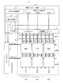
- FIG. 1 is a schematic diagram illustrating a configuration example of a liquid crystal display device 10 according to the first embodiment.
- FIG. 2 is an equivalent circuit diagram of the pixel 16 shown in FIG.
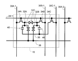
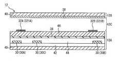
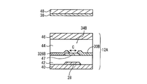
- FIG. 3 is a plan view of the pixel 16 shown in FIG. 4 is a cross-sectional view taken along the line IV-IV in FIG. 5 is a cross-sectional view taken along the line VV in FIG.
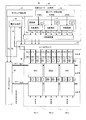
- FIG. 6 is a functional block diagram illustrating a configuration example of the liquid crystal control board 20.
- FIG. 7 is a diagram illustrating an example of a transverse electric field.
- FIG. 8 is a diagram illustrating an example of a vertical electric field.
- FIG. 9 is a diagram illustrating an example of an alignment state of liquid crystal molecules when a white display voltage is applied.
- FIG. 9 is a diagram illustrating an example of an alignment state of liquid crystal molecules when a white display voltage is applied.
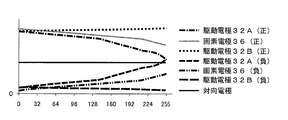
- FIG. 10 is a graph showing an example of voltage values set for each display gradation.
- FIG. 11 is a diagram illustrating an example of the pull-in voltage value in the liquid crystal display device.
- FIG. 12 is a graph showing an example of voltage values set in consideration of the pull-in voltage.
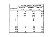
- FIG. 13 is a table showing an example of the voltage value of each electrode with respect to the display gradation value set as shown in FIG. 10 or FIG.
- FIG. 14 is a table showing an example of the output voltage value with respect to the source driver input data value (8 bits).
- FIG. 15 is a table showing an example of the contents of the LUT.
- FIG. 16 is a diagram for explaining an operation example in which a voltage signal corresponding to the display gradation value is supplied to each of the three electrodes.
- FIG. 16 is a diagram for explaining an operation example in which a voltage signal corresponding to the display gradation value is supplied to each of the three electrodes.
- FIG. 17 is a diagram illustrating an example of a configuration in which a plurality of source drivers are connected in cascade.
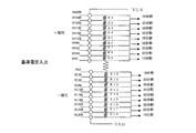
- FIG. 18 is a diagram illustrating a configuration example of a ladder in the source driver.
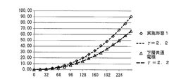
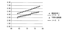
- FIG. 19 shows the characteristics of the panel output luminance for each display gradation input and the panel output luminance when the pixel electrode is shared in the liquid crystal display device 10 according to the present embodiment.
- FIG. 20 is an enlarged view of the vicinity of the gradation 70 in the graph shown in FIG.
- FIG. 21 is a functional block diagram illustrating a configuration example of the liquid crystal display device 10 according to the second embodiment.
- FIG. 22 is a diagram for explaining the operation of the source driver 24.
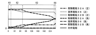
- FIG. 23 is a graph illustrating an example of voltage setting for each gradation of three electrodes in the third embodiment.
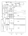
- FIG. 24 shows a wiring configuration example of the liquid crystal display device 10 according to the fourth embodiment.
- FIG. 25 is a functional block diagram illustrating a wiring configuration example of the liquid crystal display device
- a liquid crystal display device includes an active matrix substrate, a counter substrate disposed opposite to the active matrix substrate, and a liquid crystal layer sealed between the active matrix substrate and the counter substrate. Is provided.
- the active matrix substrate includes a pair of drive electrodes disposed for each pixel, a pixel electrode provided for each pixel on the opposite side of the pair of drive electrodes and the insulating layer, and the pair of drive electrodes for each pixel.
- a second source line connected to the group, a third source line provided for each pixel column and connected to a third switching element group of the pixel group included in each pixel column, and the first switching element of each pixel Has a second switching element, and a plurality of gate lines for supplying a control signal to the third switching a.
- the counter substrate includes a counter electrode disposed to face the pixel electrode and the pair of drive electrodes.
- each pixel is provided with a pair of drive electrodes and pixel electrodes arranged in an insulating layer. Accordingly, when there is a potential difference between the pair of drive electrodes, a horizontal electric field is generated, and when there is a potential difference between the pixel electrode and the counter electrode, a vertical electric field is generated.
- the pair of drive electrodes and pixel electrodes are connected to the first to third source lines via the first to third switching elements, respectively. Three source lines of the first to third source lines are provided for one pixel column. Therefore, different voltage values can be applied to the pair of drive electrodes and pixel electrodes of each pixel via the first to third switching elements and the first to third source lines.
- the voltages of the pair of drive electrodes and pixel electrodes can be controlled. Therefore, it is possible to finely control the lateral electric field between the pair of drive electrodes and the vertical electric field between the pixel electrode and the counter electrode. As a result, it becomes possible to control the direction of the electric field applied to the liquid crystal while maintaining a good balance. As a result, the transmittance of the liquid crystal layer can be controlled with high accuracy.
- the liquid crystal display device may further include a control unit that displays an image in the display area.
- the control unit applies a voltage corresponding to a gradation to be displayed in each pixel to the pixel via the first source line, the second source line, and the third source line.
- the electrode and the pixel electrode are supplied independently.
- the control unit finely controls the horizontal electric field between the pair of drive electrodes and the vertical electric field between the pixel electrode and the counter electrode, thereby generating an electric field suitable for displaying a desired gradation in each pixel. Can be applied to the layer.
- the control unit corresponds to a voltage to be applied to each of the pair of drive electrodes and the pixel electrode in each pixel based on a display gradation value indicating a gradation to be displayed in each pixel.
- a conversion unit that generates a voltage value to be included can be included.
- the conversion unit appropriately sets a voltage value for each of the pair of drive electrodes and the pixel electrode that contributes to generation of an electric field for obtaining a gradation to be displayed.
- the voltage value generated by the conversion unit may be an applied voltage itself or a voltage signal value representing a voltage to be applied.
- the voltage signal value is, for example, a value used for generating a voltage to be applied.
- the voltage value generated by the conversion unit can be a voltage or a voltage signal value.
- the control unit corresponds to all gradation values indicating all gradations that can be displayed by the pixel, voltage values of the pair of drive electrodes corresponding to the gradation values, and the gradation values.
- a conversion value recording unit that records the voltage value of the pixel electrode can be provided.
- the conversion unit refers to the conversion value recording unit for the voltage value of each of the pair of drive electrodes corresponding to the display gradation value and the voltage value of the pixel electrode corresponding to the display gradation value. decide.
- the conversion unit can appropriately set the voltage value of each of the pair of drive electrodes and the voltage value of the pixel electrode corresponding to the display gradation value.
- the conversion unit includes a drive electrode voltage generation circuit that outputs a voltage value serving as a reference voltage value of each of the pair of drive electrodes corresponding to the display gradation value, and the pixel electrode corresponding to the display gradation value It is also possible to have a pixel electrode voltage generation circuit that outputs a voltage value serving as a reference for the voltage value. Accordingly, the conversion unit can appropriately generate and output the voltage value of each of the pair of drive electrodes and the voltage value of the pixel electrode corresponding to the display gradation value of one pixel.
- the conversion unit has a voltage value of one electrode of the pair of drive electrodes, a voltage value of the other electrode of the pair of drive electrodes, or a voltage value of a part of all gradations that can be displayed by the pixel, or The voltage value may be generated so that at least one of the voltage values of the pixel electrode is constant.
- the conversion unit categorizes into several continuous ranges in all gradations that can be displayed by the pixel, and in each range, the voltage value for one electrode of the pair of drive electrodes, the pair of drive One of the voltage value of the electrode with respect to the other electrode or the voltage value of the pixel electrode is specified, and the voltage signal value within the range is determined by adjusting the specified voltage value. it can.
- Two each of the first source line, the second source line, and the third source line may be provided in each pixel column.
- Two first source lines of each pixel column are connected to each of two adjacent pixels in the pixel column, and voltage values having different polarities are simultaneously input to the two first source lines. Is done.
- Two second source lines in each pixel column are connected to each of two adjacent pixels in the pixel column, and voltages having different polarities are simultaneously input to the two second source lines.
- the Two third source lines in each pixel column are connected to each of two adjacent pixels in the pixel column, and voltages having different polarities are simultaneously input to the two third source lines.
- two adjacent gate lines corresponding to the pixel column can be simultaneously selected.
- voltages having different polarities are simultaneously input to two adjacent lines. Also good. Further, voltages having different polarities may be simultaneously input to the first source lines of two pixels adjacent to each other in a direction perpendicular to the extending direction of the first source line.
- the control unit can also time-divide one frame period and switch and display images of different colors in each time-divided period.
- the first switching element, the second switching element and the third switching element can be formed by thin film transistors.
- the thin film transistor includes a semiconductor layer including an oxide semiconductor provided at a position facing an electrode connected to the gate line, a first electrode connected to one of the pair of driving electrodes or the pixel electrode, And a second electrode connected to the source line.
- the first electrode and the second electrode are formed apart from each other on the semiconductor layer. In this manner, the arrangement area of the thin film transistor using an oxide semiconductor can be reduced. As a result, the area where the first to third switching elements are arranged is reduced, and a decrease in aperture ratio due to the addition of switching elements can be suppressed.
- FIG. 1 shows a configuration example of a liquid crystal display device 10 according to the first embodiment.
- FIG. 1 mainly shows a configuration of an active matrix substrate 12A included in the liquid crystal display device 10.
- the active matrix substrate 12A has a display area 18 in which a plurality of pixels 16 are arranged.
- a plurality of pixel columns 160-1, 160-2, 160-3,... are arranged side by side in one direction (screen horizontal direction).
- a plurality of pixels 16 are formed side by side in a direction (vertical direction in the drawing) different from the one direction. Thereby, the plurality of pixels 16 are arranged in a matrix.
- Each pixel 16 includes a pair of drive electrodes 32A and 32B and a pixel electrode 36.
- the pair of drive electrodes 32A and 32B and the pixel electrode 36 are connected to three source lines 30A-1, 30B-1, and 30C-1 through thin film transistors (hereinafter referred to as TFTs) 34A, 34B, and 34C, respectively. It is connected. That is, three source lines are connected to one pixel 16.
- TFTs thin film transistors
- each pixel 16 includes a TFT 34A connected to one of the pair of drive electrodes 32A and 32B (here, the drive electrode 32A), a TFT 34B connected to the other drive electrode 32B, and a pixel electrode 36.
- a TFT 34C to be connected is included.
- the source line connected to the TFT 34A is referred to as a first source line 30A
- the source line connected to the TFT 34B is referred to as a second source line 30B
- the source line connected to the TFT 34C is referred to as a third source line 30C.
- the first source line 30A is provided for each pixel column.
- the first source line 30A of each pixel column is connected to the TFTs 34A of a plurality of pixel groups constituting each pixel column. That is, the drive electrode 32A of the pixel group in one pixel column is connected to one first source line 30A via the TFT 34A.
- the second source line 30B and the third source line 30C are provided for each pixel column, and are respectively connected to the TFTs 34B or 34C of a plurality of pixel groups included in each pixel column.
- TFTs 34A, 34B, and 34C are examples of a first switching element, a second switching element, and a third switching element.
- the TFTs 34A, 34B, 34C of one pixel 16 are all connected to the same one gate line 28 among the plurality of gate lines 28-1, 28-2,.
- the gate line 28 is a transmission line that supplies a control signal to the TFTs 34A, 34B, and 34C.
- the gate line 28 is formed extending in a direction intersecting with the source line 30. All of the TFTs 34A, 34B, 34C of the plurality of pixels arranged in the extending direction of the single gate line 28 are connected to the single gate line 28. That is, the gate line 28 is provided for each row of pixels.
- the plurality of gate lines 28 and the plurality of source lines 30 are arranged in a lattice pattern.
- a counter substrate facing the active matrix substrate 12A is disposed so as to cover the active matrix substrate 12A.
- a liquid crystal layer is sealed between the active matrix substrate 12A and the counter substrate.
- the position of the counter electrode 38 provided on the counter substrate is indicated by a broken line.
- the counter electrode 38 is disposed at a position overlapping the pixel electrode 36 and the pair of drive electrodes 32A and 32B in plan view.
- the counter electrode 38 is formed so as to cover substantially the entire display area 18.
- the plurality of gate lines 28-1, 28-2,... are connected to the gate driver 22.
- the plurality of source lines 30 are connected to the source driver 24.
- the gate driver 22 sequentially supplies voltages Vg-1, Vg-2,... To the plurality of gate lines 28-1, 28-2,. Thereby, each row of pixels can be sequentially selected, that is, scanned.
- the source driver 24 synchronizes with the timing of selection of each gate line by the gate driver 22 to display the plurality of source lines 30A-1, 30B-1, 30C-1, 30A-2,. Voltages Vsa-1, Vsb-1, Vsc-1, Vsa-2,.
- each of the first source line 30 ⁇ / b> A, the second source line 30 ⁇ / b> B, and the third source line 30 ⁇ / b> C connected to one pixel 16 depends on the display gradation displayed on the pixel 16.
- the voltages Vsa-1, Vsb-1, and Vsc-1 are supplied separately.
- a voltage having a value corresponding to the gradation to be displayed in each pixel is independently supplied to the pair of drive electrodes 32A and 32B and the pixel electrode 36. Therefore, the lateral electric field generated by the pair of drive electrodes 32A and 32B and the vertical electric field generated by the pixel electrode 36 and the corresponding electrode 38 can be finely controlled with good balance. This operation and effect will be described later.
- the operations of the gate driver 22 and the source driver 24 can be controlled by a control circuit provided on the liquid crystal control board 20.
- the control circuit of the liquid crystal control substrate 20 can input the voltage values of the pair of drive electrodes 32A and 32B and the pixel electrode 36 in each pixel, for example, to the source driver 24.
- voltage signal values (Pa, Pb, Pc) corresponding to voltages applied to the pair of drive electrodes 32A, 32B and the pixel electrode 36 are sequentially supplied from the liquid crystal control substrate 20 to the source driver 24. Entered.
- a reference voltage value Vr serving as a reference for a voltage output to the source line corresponding to each voltage signal value and a value indicating the voltage Vt of the counter electrode 38 are input to the source driver 24.
- a gate voltage Vg supplied to each gate line is input to the gate driver 22.
- the components that control the operation for displaying an image in the display area of the liquid crystal display device 10 are the control unit 14.
- the control unit 14 can be formed by an FPC connected to the active matrix substrate 12A or a circuit or a semiconductor chip mounted on a substrate connected via the FPC.
- FIG. 2 is an equivalent circuit diagram of the pixel 16 shown in FIG.
- FIG. 3 is a plan view of the pixel 16 shown in FIG. 4 is a cross-sectional view taken along the line IV-IV in FIG. 5 is a cross-sectional view taken along the line VV in FIG.
- the gate line 28-1 is connected to three TFTs 34A, 34B, and 34C.
- the sources of the two TFTs 34A and 34B are connected to the first source line 30A-1 and the second source line 30B-1, respectively.
- the drain of one TFT 34A is connected to the drive electrode 32A
- the drain of the other TFT 34B is connected to the drive electrode 32B.
- the source of the remaining one TFT 34C is connected to the third source line 30C-1.
- the drain of the TFT 34C is connected to the pixel electrode 36.
- the drive electrodes 32A and the drive electrodes 32B are arranged to face each other in a direction parallel to the surface of the active matrix substrate 12A (details will be described later with reference to FIGS. 3 and 4).
- the drive electrode 32A and the drive electrode 32B are arranged to face the counter substrate 12B with the liquid crystal layer 12C interposed therebetween in a direction perpendicular to the surface of the active matrix substrate 12A. Therefore, in the equivalent circuit diagram shown in FIG. 2, the drive electrode 32A and the drive electrode 32B are connected via a liquid crystal capacitance by the liquid crystal layer 12C.
- the drive electrode 32A and the counter electrode 38, and the drive electrode 32B and the counter electrode 38 are also connected through a liquid crystal capacitance by the liquid crystal layer 12C.
- the pair of drive electrodes 32A and 32B are provided on an insulating layer that is a dielectric.
- the pixel electrode 36 is provided on the opposite side of the drive electrodes 32A and 32B with an insulating layer interposed therebetween (details will be described later with reference to FIG. 4). For this reason, in the equivalent circuit diagram shown in FIG. 2, the drive electrode 32 ⁇ / b> A and the pixel electrode 36, and the drive electrode 32 ⁇ / b> B and the pixel electrode 36 are also connected via a capacitor by the insulating layer 46.
- the electric field applied to the liquid crystal layer 12C between the pair of drive electrodes 32A and 32B that is, the lateral electric field varies depending on the voltage of the drive electrode 32A and the drive electrode 32B.
- the electric field applied to the liquid crystal layer 12C between the pair of drive electrodes 32A and 32B and the pixel electrode 36 and the counter electrode 38 that is, the vertical electric field varies depending on the voltages of these three electrodes.
- the voltage of the drive electrode 32A is controlled by switching according to the voltage of the first source line 30A-1 and the control signal of the gate line 28-1 of the TFT 34A.
- the voltage of the drive electrode 32B is controlled by switching according to the voltage of the second source line 30B-1 and the control signal of the gate line 28-1 of the TFT 34B.
- the voltage of the pixel electrode 36 is controlled by switching according to the voltage of the third source line 30C-1 and the control signal of the gate line 28-1 of the TFT 34C. Therefore, it is possible to finely control the vertical electric field and the horizontal electric field applied to the liquid crystal layer 12C by the voltages of the first to third source lines 30A-1, 30B-1, and 30C-1 and the switching of the TFTs 34A, 34B, and 34C. Become. Thereby, the balance between the vertical electric field and the horizontal electric field can be controlled.
- the liquid crystal display device 10 includes an active matrix substrate 12A, a counter substrate 12B, and a liquid crystal layer 12C.
- the active matrix substrate 12A includes a base substrate 40, a plurality of gate lines 28 (see FIG. 3), an insulating layer 42, a plurality of source lines 30 (a plurality of sets of source lines 30A, 30B, 30C), and an insulating layer 44.
- a pair of drive electrodes 32A, 32B, TFTs 34A, 34B, 34C see FIG. 3
- a pixel electrode 36 and an insulating layer 46.
- the plurality of gate lines 28 are formed above the main surface of the base substrate 40, for example.
- the insulating layer 42 covers the plurality of gate lines 28.
- the plurality of source lines 30 are formed on the side opposite to the plurality of gate lines 28 with the insulating layer 42 interposed therebetween.
- the insulating layer 44 covers the plurality of source lines 30.
- the pixel electrode 36 is formed in contact with the insulating layer 44.
- the pixel electrode 36 is provided for each pixel and is arranged over the entire pixel region.
- the insulating layer 46 covers the pixel electrode 36.
- the pair of drive electrodes 32 ⁇ / b> A and 32 ⁇ / b> B are formed above the insulating layer 46.
- the pixel electrode 36 is formed on the opposite side of the insulating layer 46 from the pair of drive electrodes 32A and 32B. That is, the pixel electrode 36 is disposed in a different layer from the pair of drive electrodes 32A and 32B. Further, the pixel electrode 36 is disposed farther from the liquid crystal layer 12C than the pair of drive electrodes 32A and 32B. As a result, capacitance is formed between the pixel electrode 36 and the drive electrode 32A and between the pixel electrode 36 and the drive electrode 32B.
- the TFTs 34A, 34B, and 34C are arranged at positions that overlap the gate line 28 through the gate insulating film.
- the drive electrode 32A includes a first electrode portion 321A and a plurality of second electrode portions 322A.
- the first electrode portion 321A extends in parallel with the first source line 30A and overlaps the first source line 30A in plan view.
- the plurality of second electrode portions 322A are each connected to the first electrode portion 321A.
- the plurality of second electrode portions 322A are arranged at a predetermined interval in the direction in which the first electrode portion 321A extends.
- connection electrode portion 323A is formed at the other end of the first electrode portion 321A.
- the connection electrode portion 323A has a contact hole 324A.
- the connection electrode portion 323A is connected to the drain electrode portion 326A through the contact electrode portion 325A.
- the contact electrode portion 325A is formed at a position overlapping the contact hole 324A.
- the drain electrode portion 326A is connected to the drain of the TFT 34A.
- the drive electrode 32B includes a first electrode part 321B and a plurality of second electrode parts 322B.
- the first electrode portion 321B extends in parallel with the second source line 30B and overlaps the second source line 30B in plan view.
- the plurality of second electrode portions 322B are connected to the first electrode portion 321B, respectively.
- the plurality of second electrode portions 322B are arranged at a predetermined interval in the direction in which the first electrode portion 321B extends.
- the second electrode portion 322B included in the drive electrode 32B and the second electrode portion 322A included in the drive electrode 32A are alternately arranged in the direction in which the source line 30 extends.
- connection electrode portion 323B is formed at one end of the second electrode portion 322B.
- the connection electrode portion 323B has a contact hole 324B.
- the connection electrode part 323B is connected to the drain electrode part 326B through the contact electrode part 325B.
- the contact electrode portion 325B is formed at a position overlapping the contact hole 324B.
- the drain electrode portion 326B is connected to the drain of the TFT 34B.
- the pixel electrode 36 is disposed at a position overlapping the drive electrodes 32A and 32B in plan view.
- the pixel electrode 36 is formed over the entire area of the pixel in plan view.
- a contact hole 324 ⁇ / b> C is formed at the end of the pixel electrode 36 and at a location close to the gate line 28.
- the contact hole 324C penetrates the insulating layer 44 and is connected to the contact electrode portion 325C below the insulating layer 44.
- the pixel electrode 36 is connected to the drain electrode portion 326C through the contact hole 324C and the contact electrode portion 325C.
- the contact electrode portion 325C is formed at a position overlapping the contact hole 324C.
- the drain electrode portion 326C is connected to the drain of the TFT 34C.
- the pair of drive electrodes 32A and 32B has a comb shape and is provided in a layer above the pixel electrode 36. Therefore, the drive electrode 32A may be referred to as a first upper layer comb electrode, the drive electrode 32B may be referred to as a second upper layer comb electrode, and the pixel electrode 36 may be referred to as a lower layer electrode.
- the TFT 34C is also provided in the pixel electrode 36 below the drive electrodes 32A and 32B. Therefore, the structure is such that a different voltage can be controlled for each electrode for each gradation of each pixel.
- the counter substrate 12B is disposed to face the active matrix substrate 12A.
- the counter substrate 12B includes a base substrate 48 and a counter electrode 38.
- the counter electrode 38 is formed, for example, above the main surface of the base substrate 48.
- the liquid crystal layer 12C is sealed between the active matrix substrate 12A and the counter substrate 12B.
- the liquid crystal molecules have, for example, positive dielectric anisotropy and are vertically aligned.
- FIG. 5 is a cross-sectional view showing a portion where the TFT 34B in FIG. 3 is formed.
- the gate line 28 is formed on the base substrate 40 of the active matrix substrate 12A.
- the gate line 28 and the gate of the TFT 34B are integrally formed.
- An insulating layer 42 is formed on the gate line 28 as a gate insulating film.
- a semiconductor layer 47 is formed at a position facing the gate line 28 with the insulating layer 42 interposed therebetween.
- the source line 30B and the drain electrode portion 326B are formed apart from each other. A region sandwiched between the source line 30B and the drain electrode portion 326B on the semiconductor layer 47 becomes a channel region.
- the source line 30B and the source of the TFT 34B are integrally formed.
- the drain electrode portion 326B is connected to the drive electrode 32B.
- an insulating layer 44 is provided as a protective layer that covers the semiconductor layer 47, the source line 30B, and the drain electrode portion 326B.
- the insulating layer 44 is made of an insulating film such as SiO 2.
- the insulating layer 46, the liquid crystal layer 12C, the counter electrode 38, and the base substrate 48 are provided in this order on the insulating layer 44.
- the semiconductor layer 47 includes an oxide semiconductor.
- the oxide semiconductor for example, InGaZnOx containing indium (In), gallium (Ga), zinc (Zn), and oxygen (O) as main components can be used.
- This InGaZnOx that is, an In—Ga—Zn—O-based semiconductor is a ternary oxide of In, Ga, and Zn, and the ratio (composition ratio) of In, Ga, and Zn is not particularly limited.
- the semiconductor layer 47 in this embodiment uses an In—Ga—Zn—O-based semiconductor containing In, Ga, and Zn at a ratio of 1: 1: 2.
- the TFT 18 having the semiconductor layer 47 containing an In—Ga—Zn—O-based semiconductor has a mobility of about 20 times or more and a leakage current of less than about 1/100 compared with a TFT using a-Si. is there. Therefore, such an oxide semiconductor is preferably used for a TFT for driving a pixel.
- a TFT having the semiconductor layer 47 containing an In—Ga—Zn—O-based semiconductor as the three TFTs 34A, 34B, and 34C provided in each pixel, the power consumption of the liquid crystal display device 10 can be greatly reduced. Is possible. Further, since the TFT can be reduced in size, a decrease in the aperture ratio can be suppressed by increasing the number of TFTs in the pixel.
- the In—Ga—Zn—O-based semiconductor may be amorphous or may include a crystalline part and have crystallinity.
- a crystalline In—Ga—Zn—O-based semiconductor in which the c-axis is oriented substantially perpendicular to the layer surface is preferable.
- Such a crystal structure of an In—Ga—Zn—O-based semiconductor is disclosed in, for example, Japanese Patent Application Laid-Open No. 2012-134475. For reference, the entire disclosure of Japanese Patent Application Laid-Open No. 2012-134475 is incorporated herein.
- the semiconductor layer 47 may include another oxide semiconductor instead of the In—Ga—Zn—O-based semiconductor.
- the semiconductor layer 47 includes, for example, a Zn—O based semiconductor (ZnO), an In—Zn—O based semiconductor (IZO (registered trademark)), a Zn—Ti (titanium) —O based semiconductor ( ZTO), Cd (cadmium) -Ge (germanium) -O based semiconductor, Cd—Pb (lead) —O based semiconductor, CdO (cadmium oxide) —Mg (magnesium) —Zn—O based semiconductor, In— A Sn (tin) —Zn—O based semiconductor (eg, In 2 O 3 —SnO 2 —ZnO), an In—Ga (gallium) —Sn—O based semiconductor, or the like may be included.
- ZnO ZnO
- IZO In—Zn—O based semiconductor
- ZTO Zn
- FIG. 6 is a functional block diagram illustrating a configuration example of the liquid crystal control board 20.
- the liquid crystal control board 20 includes a timing control unit 51, a display data reception unit 53, a voltage generation unit 54, and a conversion unit 55.
- the timing control unit 51 generates a signal indicating the operation timing of the gate driver 22 and the source driver 24 based on data indicating display timing input from the outside.
- the timing control unit 51 outputs, for example, a signal indicating timing for applying a voltage to the pixel to the gate driver 22 and the source driver 24.
- the display data receiving unit 53 receives input of display data from the outside.
- the display data can be a display gradation value indicating the gradation to be displayed in each pixel, for example.
- the display data receiving unit 53 can receive data representing the display gradation value of each pixel in 8 bits and output the data to the conversion unit 55.
- the conversion unit 55 generates voltage values for the pair of drive electrodes 32A and 32B and the pixel electrode 36 in each pixel based on the display gradation value of each pixel.
- the display data receiving unit 53 inputs display data representing each gradation of RGB in 8 bits.
- the conversion unit 55 includes an R conversion unit, a G conversion unit, and a B conversion unit that convert display gradation values into voltage signal values of the pair of drive electrodes 32A and 32B and the pixel electrode 36 for each of RGB.
- the RGB color conversion unit in the conversion unit 55 refers to a look-up table (LUT) to acquire voltage signal values of the pair of drive electrodes 32A and 32B and the pixel electrode 36 corresponding to the display gradation values. Can do.
- the LUT is an example of a conversion value recording unit that records the voltage signal value of each of the pair of drive electrodes 32A and 32B corresponding to the display gradation value and the voltage signal value of the pixel electrode 36 corresponding to the display gradation value. is there.
- the conversion unit 55 is configured to convert the display gradation value to the voltage signal value of each electrode, but the conversion unit 55 is configured to convert the display gradation value to the voltage of each electrode. You can also.
- the voltage signal values of the pair of drive electrodes 32A and 32B converted by the conversion unit 55 and the voltage signal value of the pixel electrode 36 are output to the source driver 24 with a clock converted to triple speed. .
- three voltage signal values are output to the source driver 24 for one pixel.
- the R pixel data, the G pixel data, and the B pixel data are sequentially output to the source driver 24 at a one-third cycle.
- the voltage signal value Pa-1 of the drive electrode 32A, the voltage signal value Pb-1 of the drive electrode 32B, and the voltage signal value Pc-1 of the pixel electrode 36 are first obtained. It is output to the source driver 24. Thereafter, the voltage signal values Pa-2, Pb-2, and Pc-2 are output to the source driver 24 for the green (G) pixel 16 (G). Thereafter, the data of the voltage signal values Pa-3, Pb-3, and Pc-3 is output to the source driver 24 for the blue (B) pixel 16 (B). As described above, the voltage signal value data is transferred to the source driver 24 with three times the clock via the three signal lines, and is used to transfer the gradation value data of the conventional RGB three pixels. Data of three voltage signal values can be transferred per pixel with the same wiring configuration as that used.
- the source driver 24 supplies voltage values based on the three voltage signal values Pa-1, Pb-1, and Pc-1 of the pixel 16 (R) to the source lines 30A-1, 30B- connected to the pixel 16 (R). 1 and output to 30C-1.
- the source driver 24 applies voltages based on the three voltage signal values Pa-2, Pb-2, and Pc-2 of the pixel 16 (G) to the source line 30A-2 connected to the pixel 16 (G), 30B-2 and 30C-2 are supplied with voltages based on the three voltage signal values Pa-3, Pb-3, and Pc-3 of the pixel 16 (B) and the source line 30A-3 connected to the pixel 16 (B). , 30B-3, 30C-3.
- the voltage generator 54 generates a voltage Vg applied to the gate line 28 by the gate driver 22, a voltage Vr serving as a reference for generating a voltage applied to the source line 30 by the source driver 24, and a voltage Vt applied to the counter electrode 38. Generate and output to the gate driver 22 and the source driver 24.
- the voltage Vr applied to the source line 30 can be a reference voltage value.
- the reference voltage value is a part of the voltage value applied to the pixel and is a reference voltage.
- the source driver 24 can generate the voltage of each pixel corresponding to the gradation to be displayed based on the reference voltage and the input voltage signal value.
- the counter electrode voltage is constant, and the voltage applied to the source line is dot inversion driving (driving method in which the polarity is inverted for each pixel). it can. In this case, the following operation is possible.
- an input display data signal and display timing data are input to the liquid crystal control board 20.
- the display data receiving unit 53 inputs data indicating the display gradation value of each color (RGB) of the display data to the R conversion unit, the G conversion unit, and the B conversion unit of the conversion unit 55, respectively.
- the conversion unit 55 converts the input display gradation value into data indicating the voltage signal value corresponding to each pixel electrode (data for the drive electrode 32A, data for the drive electrode 32B, data for the pixel electrode 36), Data is transferred to the source driver 24.
- the data of each pixel held in the source driver 24 is based on the reference voltage generated by the voltage generator. It is converted into a voltage corresponding to the signal value and output to the source line 30.
- data of three voltage signal values (data for the drive electrode 32A, data for the drive electrode 32B, and data for the pixel electrode 36) are converted into voltages and output to the three source lines for each pixel.
- the gate line 28 of the pixel to be written is turned ON (voltage high).
- the gate line 28 and the source line 30 are connected via TFTs 34A, 34B, and 34C.
- the gate line 28 is ON, the voltage value of the source line 30 is applied to each electrode. Thereafter, when the gate line is turned off (voltage is low), the electric charge corresponding to the voltage applied to each electrode is held.
- the polarity of the voltage signal output from the source driver 24 can be controlled to alternate between positive and negative for every three source lines. It is also possible to control so that the polarity changes for each pixel line. That is, in one frame period, in a pixel column along the source line, control may be performed so that voltage signals having different polarities are supplied to two adjacent pixels. Accordingly, the polarity of the voltage signal can be changed for each line also in the vertical direction of the display region 18. Further, it is possible to drive so that the polarity of each pixel is inverted every frame.
- the voltage value of the pixel electrode 36 in the lower layer can be changed depending on the gradation.
- the technical significance of changing the voltage value of the lower pixel electrode 36 for each gradation will be described.
- Non-Patent Document 1 describes a mode in which gradation display is performed by controlling the direction of liquid crystal molecules using a vertical electric field and a horizontal electric field by four electrodes.
- liquid crystal molecules having positive dielectric anisotropy are used. Therefore, in the white display, a lateral electric field is applied by a potential difference between the pair of drive electrodes 32A and 32B so that the major axis direction of the liquid crystal molecules faces the horizontal direction with respect to the glass substrate (see FIG. 7).
- a vertical electric field is applied between the counter electrode 38 and the pixel electrode 36 (lower layer electrode) so that the major axis direction of the liquid crystal molecules is oriented in a direction perpendicular to the base substrate 40 (see FIG. 8).
- Non-Patent Document 1 when the lower layer electrode is a common electrode (common to the pixels in the panel), a vertical electric field similar to that for black display is applied even in white display. In that case, it becomes difficult to tilt the liquid crystal molecules sufficiently in the horizontal direction on the base substrate 40.
- the transmittance of the panel pixels can be controlled and gradation display can be performed.
- the balance between the vertical electric field and the horizontal electric field can be adjusted by providing a structure in which the lower electrode is not provided in common and is provided for each pixel and the voltage of the lower electrode can be controlled in accordance with the display gradation.
- the alignment direction of the liquid crystal molecules is controlled, and appropriate gradation display is possible.
- This also improves the response speed of the liquid crystal molecules because the alignment direction of the liquid crystal molecules is controlled by a combination of a horizontal electric field and a vertical electric field.
- Voltage value setting example 1 An example of setting the voltage values of the pair of drive electrodes 32A and 32B and the pixel electrode 36 for each gradation will be described.
- a voltage setting example in the case where the voltage of the counter electrode 38 is constant and the drive electrodes 32A and 32B and the pixel electrode 36 of each pixel are driven by dot inversion will be described.
- Vm is a value in consideration of the dielectric constant and thickness of the liquid crystal layer and the dielectric constant and thickness of the insulating layer 46.
- the dielectric constant of the liquid crystal layer is the dielectric constant when the major axis direction of the liquid crystal molecules is aligned so as to be perpendicular to the glass substrate.
- the dielectric constant is expressed by ⁇ _lc //
- the thickness of the liquid crystal layer is When dl and the dielectric constant and thickness of the insulating layer 46 are expressed as ⁇ _m and dm, respectively, Vm can be expressed by the following equation.
- Vm (dm / dl) ⁇ ( ⁇ _lc /// ⁇ _m) ⁇ Vp
- a specific voltage setting value can be set as follows.
- Counter electrode 38 7.5V (constant) Drive electrode 32A: 14.5V (positive), 0.5V (negative) Drive electrode 32B: 14.5V (positive), 0.5V (negative)
- Pixel electrode 36 15.0V (positive), 0.0V (negative)
- the insulating layer 46 is designed to have a dielectric constant and a thickness that satisfy the above conditions.
- Vh alternating current
- Counter electrode 38 Vc (constant) Drive electrode 32A: Vc (positive), Vc (negative) (both polarities have the same potential as the counter electrode)
- Drive electrode 32B Vc + Vh (positive), Vc-Vh (negative) (positive polarity and negative polarity are reversed for each frame)
- Pixel electrode 36 Vc + Vn (positive), Vc-Vn (negative) (positive polarity and negative polarity are reversed for each frame)
- Vn is a potential difference between the drive electrode 32A and the pixel electrode 36 and a potential difference between the drive electrode 32B and the pixel electrode 36 so that the balance of the lateral electric field applied between the drive electrodes 32A and 32B of the liquid crystal layer 12C is improved.
- Vn can be set, for example, as in the following equation.
- a specific voltage setting value can be as follows.
- Counter electrode 38 7.5V (constant) Drive electrode 32A: 7.5V (positive), 7.5V (negative) (positive and negative polarity are reversed for each frame)
- Drive electrode 32B 15.0V (positive), 0.0V (negative) (positive polarity and negative polarity are reversed for each frame)
- Pixel electrode 36 11.25V (positive), 3.75V (negative) (positive polarity and negative polarity are reversed for each frame)
- FIG. 9 is a diagram illustrating an example of the alignment state of liquid crystal molecules when the white display voltage is applied to the counter electrode 38, the drive electrodes 32A and 32B, and the pixel electrode 36.
- the display surface of the liquid crystal layer 12C is generated by a horizontal electric field between the drive electrode 32A and the drive electrode 32B and a vertical electric field between the counter electrode 38, the drive electrodes 32A and 32B, and the pixel electrode 36.
- the electric lines of force along the direction parallel to are distributed in a well-balanced manner.
- the drive electrode 32 ⁇ / b> B and the counter electrode 38 have the same potential when a white display voltage is applied. Therefore, there is almost no vertical electric field on the drive electrode 32B. Accordingly, for example, as compared with the voltage setting in which the vertical electric field is generated as shown in FIG. 7, the major axis direction of the liquid crystal molecules at the time of applying the voltage for white display is easily oriented horizontally, and the transmittance is improved.
- the counter substrate 12 ⁇ / b> B includes the dielectric layer 52.
- the dielectric layer 52 is disposed closer to the liquid crystal layer 12C than the counter electrode 38 is.
- the dielectric layer 52 is made of, for example, an organic film, an ultraviolet curable resin, or a thermosetting resin. In such an embodiment, when a lateral electric field is generated, the liquid crystal molecules near the counter electrode 38 are likely to fall down. Therefore, the transmittance is improved.
- the voltage of each electrode can be set based on the desired ⁇ for the halftone between black and white.
- the voltages of the drive electrodes 32A and 32B and the pixel electrode 36 are set to a voltage between the white voltage and the black voltage in both positive and negative polarities.
- FIG. 10 is a graph showing an example of voltage values set for each display gradation in this way.
- the horizontal axis represents the display gradation
- the vertical axis represents the voltage of each electrode (drive electrodes 32A and 32B and pixel electrode 36).
- a display gradation of 0 indicates black display
- a display gradation of 255 indicates white display.
- the display gradation is set such that the potential difference between the drive electrode 32A and the drive electrode 32B increases as the display gradation approaches the white display from the black display.
- the potential difference between the pixel electrode 36 and the drive electrode 32A and the potential difference between the pixel electrode 36 and the drive electrode 32B are also set to increase as the display gradation approaches from black display to white display.
- the voltage of each electrode is set so that the potential difference between the pixel electrode 36 and the drive electrode 32A and the potential difference between the pixel electrode 36 and the drive electrode 32B are substantially equal. ing.
- Voltage value setting example 2 In setting the voltages of the drive electrodes 32A and 32B and the pixel electrode 36, a voltage in consideration of the gate pull-in voltage can be set. In each pixel, the gate voltage of the TFT 34 is changed by a control signal of the gate line 28 to switch the TFT 34 on / off. At this time, the voltage of the electrode connected to the drain of the TFT 34 may be affected and change due to a drop in the gate voltage. This change is the gate pull-in voltage.
- the source driver 24 can output a voltage signal corrected by an amount corresponding to the pull-in voltage to the source line 30. That is, the voltage applied as the source line voltage can be set including a component that cancels the gate pull-in voltage.
- the pull-in voltage ⁇ Vgd can be expressed by the following equation, for example.
- ⁇ Vgd Cgd / ⁇ (Clc + Cs + Co + Cgd) ⁇ (Vgh ⁇ Vgl)
- Clc is the capacitance between the counter electrode 38 and the pixel electrode 36 or the drive electrodes 32A and 32B in the liquid crystal orientation of the display gradation
- Cs is the capacitance between the source line and the pixel electrode 36 or the drive electrodes 32A and 32B
- Cgd is a capacitance between the gate line and the pixel electrode 36 or the drive electrodes 32A and 32B (including the gate-drain capacitance of the TFT)
- Co is a capacitance coupled to other electrodes
- Vgh and Vgl are gate ON voltages.
- the gate OFF voltage is the pixel electrode 36 and the pair of drive electrodes 32A and 32B are connected to the TFTs 34A, 34B, and 34C, respectively.
- the drive electrodes 32A and 32B and the pixel electrode 36 have different parameter values for determining the value of ⁇ Vgd. That is, the pull-in voltage value is not the same between the drive electrodes 32A and 32B and the pixel electrode 36. Therefore, it is preferable to estimate the pull-in voltage at each gradation in each of the drive electrodes 32A and 32B and the pixel electrode 36.
- the graph of FIG. 11 shows an example of the pull-in voltage value in the liquid crystal display device of the present embodiment.
- the change by the gradation is shown.
- This pull-in voltage value is a value for the counter electrode.
- FIG. 12 is a graph showing a setting example of the voltage applied to the source line of the pixel electrode 36 or the drive electrodes 32A and 32B in consideration of the pull-in voltage.
- a method of adjusting the pull-in voltage by adjusting the reference voltage of the source driver 24 is also conceivable.
- three source lines are connected to one pixel, and TFTs having different pull-in voltages are connected to the three source lines.
- the TFTs 34A and 34B of the drive electrodes 32A and 32B and the TFT 36 of the pixel electrode 36 may have different characteristics or electrode capacities.
- the pull-in voltage values of the drive electrodes 32A and 32B and the pixel electrode 36 are different for each gradation.
- the adjustment by the reference voltage can only correct the voltage value common to the three source lines, and may not be able to correct the voltage corresponding to each of the TFTs having different pull-in voltages.
- the voltage value for each gradation can be set for each of the drive electrodes 32A and 32B and the pixel electrode 36 in consideration of the pull-in voltage. Accordingly, the conversion unit 55 can generate a voltage signal value that obtains a voltage value set in consideration of the pull-in voltage as described above, based on the display gradation value.
- FIG. 13 is a table showing an example of the voltage value of each electrode with respect to the display gradation value set as shown in FIG. 10 or FIG.
- the ladder of the source driver 24 can be designed so that these voltage values can be output, and the reference voltage value can be determined.
- the output voltage value for the source driver input data value (8 bits) is, for example, as shown in the table of FIG. In this example, when the input data value shown in the left column of the table is input to the source driver 24, the source driver 24 displays the corresponding voltage in the center column when the polarity is positive, and the right column when the polarity is negative. The corresponding voltage signal is output to the source line.
- a table LUT
- the conversion unit 55 can convert the display gradation value into input data values (an example of voltage signal values) of the drive electrodes 32A and 32B and the pixel electrode 36 with reference to this table.
- FIG. 15 shows an example of the contents of such a table.
- FIG. 16 illustrates an operation example in which the display gradation value is converted into voltage signal values of the drive electrodes 32A and 32B and the pixel electrode 36, and a voltage corresponding to the converted voltage signal value is supplied to each of these electrodes. It is a figure for doing.
- the liquid crystal display device 10 receives display data and a clock signal CLK from the host system. For example, 8-bit data indicating each RGB display gradation is input as the display data.
- the RGB display gradation values are converted into three data values (voltage signal value data) corresponding to the drive electrodes 32A and 32B and the pixel electrode 36 by the conversion unit 55 (see FIG. 6), respectively.
- the conversion unit 55 can refer to, for example, a table (LUT) as shown in FIG.
- the input RGB (8 bits each) display data is converted into voltage signal value data (8 bits each) corresponding to the display gradation of the three electrodes (drive electrode 32A, drive electrode 32B, pixel electrode 36).
- the converted voltage signal value data is input to the source driver 24 in the order of RGB with the clock tripled by the triple speed conversion circuit.
- the order of RGB can be matched to the order of the pixel configuration in the panel.
- the source driver 24 receives a start pulse St, a latch LS, a REV signal, a CLK (clock signal), converted voltage signal value data of each electrode, and a reference voltage value.
- the REV signal is a signal for controlling the polarity of the voltage output to the source line, that is, the positive polarity (+) or the negative polarity ( ⁇ ).
- the reference voltage can be a voltage corresponding to some voltage signal values among the voltages applied to the pixel electrodes. For example, in the case of an 8-bit output source driver, a voltage corresponding to data from 0 to 255 is output by polarity, but one voltage for every 16 outputs such as 0, 16, 32,. A voltage corresponding to the signal value can be used as a reference voltage. Further, two reference voltages are set for one voltage signal value: a voltage in the case of positive polarity and a voltage in the case of negative polarity.
- the positive reference voltages can be VH255, VH248, VH232,..., VH16, VH0
- the negative reference voltages can be VL0, VL16,..., VL248, VL255.
- the reference voltage value input to the source driver of this embodiment can be set so that, for example, the output of the voltage value shown in FIG. 10 or FIG. 12 is satisfied.
- the source driver 24 is configured by connecting a plurality of source drivers in cascade.
- the St_0 signal is input to the first source driver 24
- voltage signal value data is stored in the source driver 24 for each CLK.
- the St_1 signal is sent to the next source driver.
- the voltage signal value data is stored in the next source driver that has received the St_1 signal.
- the LS signal is input at a timing when a voltage corresponding to the voltage signal value data in one horizontal period is output to the panel.
- an output voltage value based on the reference voltage for each voltage signal value data is output to the source line.
- three outputs correspond to one pixel.
- the respective voltages are output from the respective three source lines to the pixel columns of the R pixel, the G pixel, and the B pixel.
- a voltage having a polarity determined by the REV signals 0 and 1 is output to the source line.
- the source driver 24 operates so that outputs to three consecutive source lines have the same polarity.
- the source driver is designed so that the polarity is inverted every three outputs.
- data transfer to the source driver 24 is performed by triple the clock frequency and display data transfer.
- the output of the source driver 24 is output so that the output polarity is inverted every three outputs.
- dot inversion driving is realized by inverting the polarity for each frame.
- FIG. 18 is a diagram illustrating a configuration example of a resistance ladder in the source driver. In the example shown in FIG. 18, the voltage signal value data is converted into a voltage value by the resistance ladder and output to the source line.
- positive voltages corresponding to voltage signal values 255, 248, 232,..., 16, 0 are input to the ladder as reference voltages VH255, VH248, VH232,..., VH16, VH0.
- negative voltages corresponding to the voltage signal values 0, 16, 32,..., 248, 255 are input to the ladder as reference voltages VL0, VL16,.
- the positive voltage of the voltage signal value 254 is a voltage one step lower than VH255 among the voltages obtained by dividing the reference voltage VH255 and VH248 into 16 levels.
- the voltage of the three electrodes is controlled by the driving method and the voltage setting method described above.
- the white transmittance (brightness) and contrast can be improved, and in the gradation display, the transition of the display gradation at the low gradation can be made smooth.
- FIG. 19 is a graph showing the panel output luminance characteristics for each display gradation input when the liquid crystal display device 10 is driven.
- the horizontal axis represents display input data
- the vertical axis represents panel output luminance.
- the square plot represents the panel output luminance for each display gradation input in the liquid crystal display device 10.
- the triangular plot represents the panel output luminance for each display gradation input when the pixel electrode, that is, the lower layer electrode is made common to all the pixels in the display region.
- FIG. 20 is an enlarged view of the vicinity of the gradation 70 in the graph shown in FIG.
- the voltage setting for realizing a desired gamma value characteristic is achieved. It becomes easy.
- the liquid crystal response characteristics are improved due to the display mode using four electrodes, and a high-speed response is possible even at a low temperature, and the display quality is improved.
- FIG. 21 shows a configuration example of the liquid crystal display device 10 according to the second embodiment.
- the source driver 24 converts the display gradation value of each pixel indicated by the input display data into the voltage signal value voltage value of each of the three electrodes of the drive electrode 32A, the drive electrode 32B, and the pixel electrode 36. It is configured to That is, in the liquid crystal control board 20, data conversion to each electrode is not performed, and the input display data (display gradation value) of each color (RGB) is input to the source driver 24 as it is.
- a conversion unit 55 is provided in the source driver 24 for converting the display gradation value into the voltage signal value of the three electrodes. Therefore, the source driver 24 can include a resistance ladder corresponding to the LUT or each of the three electrodes.
- FIG. 22 is a diagram for explaining the operation of the source driver 24.
- RGB display gradation values are input to the source driver 24 as display data.
- the source driver 24 includes a conversion unit 55 having an LUT.
- the converter 55 converts the display gradation value into voltage signal values for the three electrodes.
- the source driver 24 generates a voltage corresponding to the converted voltage signal value using the reference voltage, and outputs the voltage to the source line connected to the three electrodes.
- the conversion is performed using the LUT.
- the source driver 24 may be provided with three types of ladders corresponding to the three electrodes.
- the three types of ladders can generate voltage values to be supplied to the three electrodes using the three types of gradation reference voltages corresponding to the three electrodes and the input display gradation values. .
- a ladder for the pixel electrode 36 that outputs a voltage of the pixel electrode 36 corresponding to the input display gradation value can be provided in the source driver 24.
- three voltages corresponding to the pair of drive electrodes 32A and 32B and the pixel electrode of the pixel are generated.
- a circuit for converting gradation value data into a voltage signal can generate a voltage of three electrodes from the gradation value of one pixel.
- FIG. 23 is a graph illustrating an example of voltage setting for each gradation of the three electrodes of the drive electrodes 32A and 32B and the pixel electrode 36 in the third embodiment.
- the voltage setting method is controlled so as to change all the voltages of the three electrodes in each gradation.
- the liquid crystal display device 10 according to the present embodiment divides the gradation into a plurality of regions, fixes one or two voltages of the three electrodes in each region, and adjusts the voltages of the other electrodes to the levels. It is a form that changes according to the key.
- all gradations are divided into four regions, a low gradation region K1, a low gradation region K2, an intermediate gradation region K3, and a high gradation region K4.
- the liquid crystal display device 10 changes the voltage in accordance with the gradation only in one of the three electrodes in each gradation region. Specifically, in the low and low gradation region K1, the voltage of the drive electrode 32B changes with gradation, and the voltages of the other electrodes do not change. In the low gradation region K2, the voltage of the pixel electrode 36 changes with respect to the gradation. In the intermediate gradation range K3, the drive electrode 32A changes.
- the voltage of the pixel electrode 36 again changes according to the gradation. That is, in this example, all gradations are classified into a plurality of continuous ranges, and in each range, one voltage signal value of the pair of drive electrodes 32A and 32B and the pixel electrode 36 is specified and specified. The voltage signal value is adjusted.
- an LUT indicating the correspondence between the display gradation value and the voltage of the three electrodes as shown in FIG. 23 can be recorded in advance.
- the conversion unit 55 can perform the driving by generating the gradation values or voltage values of the three electrodes with reference to the LUT.
- the example shown in FIG. 23 is a form in which the voltage of only one of the three electrodes is changed in all four regions K1 to K4, but the form of the voltage change of each electrode is not limited to this.
- the voltage of only one electrode can be changed in at least one of the four regions K1 to K4.
- the method of dividing the region is not limited to the four regions K1 to K4 shown in FIG.
- FIG. 24 shows a wiring configuration example of the liquid crystal display device 10 according to the fourth embodiment.
- two first source lines 30A, two second source lines 30B, and three third source lines 30C are provided in each pixel column along the source line.
- the two first source lines 30A-1a and 30A-1b in each pixel column are two pixels 16-1 and 16 adjacent to each other in the scanning direction of the gate lines 28-1 and 28-2 in this pixel column. -One is connected to each. That is, one of the two first source lines 30A-1b is connected to the TFT 34A of the pixel 16-1, and the other first source line 30A-1a is connected to the pixel column, that is, in the scanning direction of the gate signal.
- the two second source lines 30B-1a and 30B-1b in each pixel column are two pixels 16-1 and 16- adjacent to each other in the scanning direction of the gate lines 28-1 and 28-2 in the pixel column. One is connected to each two. These two second source lines 30B-1a and 30B-1b are simultaneously input with voltages having different polarities.
- the two third source lines 30C-1a and 30C-1b in each pixel column include two pixels 16-1 and 16- adjacent to each other in the scanning direction of the gate lines 28-1 and 28-2 in the pixel column. One is connected to each two. These two third source lines 30C-1a and 30C-2 are simultaneously input with voltages having different polarities.
- voltages having different polarities are simultaneously input to two adjacent source lines.
- a positive polarity voltage is applied to the first source line 30A-1b
- a negative polarity voltage is simultaneously input to the adjacent first source line 30A-1a and the second source line 30B-1a.
- positive and negative voltages are alternately input simultaneously to the plurality of source lines 30A-1a, 30A-1b, 30B-1a, 30B-1b,.
- voltages having different polarities are simultaneously applied to the first source lines 30A-1b and 30A-2a of the two pixels 16-1 and 16-3 adjacent to each other in the direction perpendicular to the extending direction of the first source line 30A.
- the first source lines of two pixels adjacent in the direction along the gate line 28 have different voltage polarities.
- dot inversion driving can be performed efficiently.
- the polarity of the voltage can be varied for each continuous source line.
- the polarity of the voltage of the even-numbered source line among the plurality of source lines can be made different from the polarity of the voltage of the odd-numbered source line.
- FIG. 25 shows a wiring configuration example of the liquid crystal display device 10 according to the fifth embodiment.
- the liquid crystal display device 10 illustrated in FIG. 25 performs time-division of one frame period, and performs so-called field sequential driving in which the different color images are switched and displayed in each time-division period.
- RGB data indicating RGB display gradation values in one frame input as display data is stored in the frame memory 27.
- One frame period is time-divided into a plurality of fields corresponding to RGB colors.
- data indicating the gradation value of the corresponding color image is read from the frame memory 27 and displayed.
- the timing control unit 51 synchronizes the timing of irradiating light of each color with the backlight and the timing of displaying the image of each color with the timing signals Tf, Ts, Tg, and Tb, the frame memory 27, the source driver 24, and the gate. Transmit to the driver 22 and the backlight 25.
- the conversion unit 55 converts the display gradation value of each pixel read from the frame memory 27 into the voltage signal value or voltage value of each of the three electrodes of the drive electrode 32A, the drive electrode 32B, and the pixel electrode 36.
- the configuration of the conversion unit 55, the source driver 24, the source line 30, the gate line 28, and the pixel 16 has a configuration of any one of the first to fourth embodiments or a combination of at least two of the first to fourth embodiments. Can be adopted.
- the liquid crystal display device when used for field sequential display, it is driven at a refresh rate of at least three times in the case of three colors. Therefore, a high-speed response is required.
- the liquid crystal display mode of this embodiment can respond quickly.
- the liquid crystal molecules have a positive dielectric anisotropy, but the liquid crystal molecules may have a negative dielectric anisotropy.
Landscapes
- Physics & Mathematics (AREA)
- Engineering & Computer Science (AREA)
- General Physics & Mathematics (AREA)
- Nonlinear Science (AREA)
- Chemical & Material Sciences (AREA)
- Crystallography & Structural Chemistry (AREA)
- Computer Hardware Design (AREA)
- Theoretical Computer Science (AREA)
- Mathematical Physics (AREA)
- Optics & Photonics (AREA)
- Geometry (AREA)
- Microelectronics & Electronic Packaging (AREA)
- Liquid Crystal (AREA)
- Control Of Indicators Other Than Cathode Ray Tubes (AREA)
Abstract
液晶表示装置(10)のアクティブマトリクス基板(12A)は、画素ごとに配置された一対の駆動電極(32A、32B)と、画素ごとに設けられる画素電極(36)と、駆動電極(32A)の一方に接続される第1スイッチング素子(34A)と、駆動電極(32B)に接続される第2スイッチング素子(34B)と、画素電極(36)に接続される第3スイッチング素子(34C)と、第1スイッチング素子(34)群に接続される第1ソース線(30A)と、第2スイッチング素子(34B)群に接続される第2ソース線(30B)と、第3スイッチング素子(30C)群に接続される第3ソース線(30C)と、複数のゲート線(28)と、を有する。
Description
本発明は、液晶表示装置に関し、詳しくは、縦電界と横電界を併用して液晶分子の配向を制御する液晶表示装置に関する。
液晶表示装置における液晶の動作モードには、縦電界を利用する動作モードや、横電界を利用する動作モードがある。縦電界は、液晶層を挟んで配置される一対の基板間に発生する。横電界は、液晶層を挟んで配置される一対の基板のうち一方の基板が有する電極間に発生する。縦電界を利用する動作モードは、例えば、TN(twisted nematic)モードやVA(vertical alignment)モードである。横電界を利用する動作モードは、例えば、IPS(in-plane switching)モードである。
また、近年では、縦電界と横電界を併用して液晶分子の配向を制御する液晶表示装置が提案されている。下記特許文献1では、縦電界により液晶の立ち上がり応答期間における配向状態を制御し、横電界によって液晶の立ち下り応答期間における配向状態を制御することが記載されている。下記特許文献2は、画像表示期間では、横電界により液晶を駆動し、画像非表示期間の初期段階では、縦電界により液晶を駆動することを開示している。下記特許文献3には、縦電界を印加した状態から印加しない状態に切り替える際に、横電界を印加する液晶装置が開示されている。
さらに、下記非特許文献1には、4つの電極により、縦電界と横電界を液晶層に同時にかける構成が提案されている。この非特許文献1では、横電界と縦電界を同時に液晶にかけることにより、液晶分子の配向を強制的に制御するV-IP駆動モードが紹介されている。これにより、低温においても高速な応答が可能になる。
DIGEST of SID 2013, pp431-434,(34.1), Y. Iwata et al. "Novel Super-Fast-Response, Ultra-Wide Temperature Range VA-LCD"
上記従来技術のように縦電界と横電界を併用して液晶分子の配向を制御する液晶表示装置では、画素内の横電界は、一方のガラス基板上に形成された一対の電極間の電位差により形成される。そのため、横電界は、ガラス基板間の液晶層のガラス基板法線方向で一様に同じ横電界とはならない。横電界が画素内のガラス基板法線方向で一様でないため、ある適当な1つの縦電界とある適当な1つの横電界を印加した場合、そのバランスによっては、画素内の液晶層の液晶分子の配向方向はいくつかの安定状態を持ってしまう場合がある。いくつかの安定状態がある場合は、印加電圧に対して、透過率が1対1にならず、正確な階調表示ができなくなってしまう。そのため、本願は、より正確な階調表示をするために縦電界と横電界のバランスを制御することができる液晶表示装置を開示する。
本発明の実施形態における液晶表示装置は、複数の画素が並んで形成される画素列が複数配置される表示領域を有するアクティブマトリクス基板と、前記アクティブマトリクス基板に対向して配置される対向基板と、前記アクティブマトリクス基板と前記対向基板との間に封入される液晶層とを備える。前記アクティブマトリクス基板は、画素ごとに絶縁層の上に配置される一対の駆動電極と、前記一対の駆動電極と前記絶縁層を挟んで反対側に、画素ごとに設けられる画素電極と、各画素の前記一対の駆動電極の一方に接続される第1スイッチング素子と、各画素の前記一対の駆動電極の他方に接続される第2スイッチング素子と、各画素の前記画素電極に接続される第3スイッチング素子と、画素列ごとに設けられ、各画素列に含まれる画素群の第1スイッチング素子群に接続される第1ソース線と、画素列ごとに設けられ、各画素列に含まれる画素群の第2スイッチング素子群に接続される第2ソース線と、画素列ごとに設けられ、各画素列に含まれる画素群の第3スイッチング素子群に接続される第3ソース線と、各画素の前記第1スイッチング素子、第2スイッチング素子、及び第3スイッチングへ制御信号を供給する複数のゲート線と、を有する。前記対向基板は、前記画素電極及び前記一対の駆動電極に対向して配置される対向電極を有する。
本発明の実施形態における液晶表示装置においては、縦電界と横電界のバランスを制御することができる。
本発明の実施の形態による液晶表示装置は、アクティブマトリクス基板と、前記アクティブマトリクス基板に対向して配置される対向基板と、前記アクティブマトリクス基板と前記対向基板との間に封入される液晶層とを備える。前記アクティブマトリクス基板は、画素ごとに配置される一対の駆動電極と、前記一対の駆動電極と前記絶縁層を挟んで反対側に、画素ごとに設けられる画素電極と、各画素の前記一対の駆動電極の一方に接続される第1スイッチング素子と、各画素の前記一対の駆動電極の他方に接続される第2スイッチング素子と、各画素の前記画素電極に接続される第3スイッチング素子と、画素列ごとに設けられ、各画素列に含まれる画素群の第1スイッチング素子群に接続される第1ソース線と、画素列ごとに設けられ、各画素列に含まれる画素群の第2スイッチング素子群に接続される第2ソース線と、画素列ごとに設けられ、各画素列に含まれる画素群の第3スイッチング素子群に接続される第3ソース線と、各画素の前記第1スイッチング素子、第2スイッチング素子、及び第3スイッチングへ制御信号を供給する複数のゲート線と、を有する。前記対向基板は、前記画素電極及び前記一対の駆動電極に対向して配置される対向電極を有する。
上記構成においては、各画素に、絶縁層に配置される一対の駆動電極と画素電極が設けられる。これにより、一対の駆動電極間の電位差がある場合には、横電界が発生し、画素電極及び対向電極間に電位差がある場合には縦電界が発生する。一対の駆動電極と画素電極は、それぞれ、第1~第3スイッチング素子を介して、第1~3ソース線に接続される。第1~3ソース線の3本のソース線が、1本の画素列に対して設けられる。そのため、各画素の一対の駆動電極及び画素電極のそれぞれに対して、第1~第3スイッチング素子及び第1~第3ソース線を介して、別々の電圧値を印加することが可能になる。すなわち、一対の駆動電極及び画素電極それぞれの電圧を制御することができる。そのため、一対の駆動電極間による横電界と、画素電極と対向電極による縦電界とを、それぞれ細かく制御することが可能になる。その結果、液晶に印加される電界の向きを精度よくバランスをとりながら制御することが可能になる。ひいては、液晶層の透過率を高精度で制御することが可能になる。
上記の液晶表示装置は、前記表示領域に画像を表示させる制御部をさらに備えることができる。前記制御部は、画素に対して、各画素で表示すべき階調に対応する電圧を、前記第1ソース線、前記第2ソース線、及び前記第3ソース線を介して、前記一対の駆動電極及び前記画素電極にそれぞれ独立して供給する。これにより、制御部は、一対の駆動電極間による横電界と、画素電極と対向電極による縦電界とを細かく制御することにより、各画素で所望の階調を表示するのに適した電界を液晶層に印加することができる。
上記液晶表示装置において、前記制御部は、各画素で表示すべき階調を示す表示階調値に基づいて、前記各画素における前記一対の駆動電極及び前記画素電極それぞれに印加すべき電圧に対応する電圧値を生成する変換部を含むことができる。変換部により、表示すべき階調を得るための電界の生成に寄与する一対の駆動電極及び前記画素電極のそれぞれの電極に対する電圧値が適切に設定される。ここで、変換部により生成される電圧値は、印加する電圧そのものであってもよいし、印加すべき電圧を表す電圧信号値であってもよい。電圧信号値は、例えば、印加すべき電圧を生成するために用いられる値である。このように、変換部により生成される電圧値は、電圧又は電圧信号値とすることができる。
前記制御部は、前記画素で表示され得る全ての階調を示す全階調値と、前記全階調値に対応する前記一対の駆動電極それぞれの電圧値、及び、前記全階調値に対応する前記画素電極の電圧値を記録した変換値記録部を有することができる。前記変換部は、前記表示階調値に対応する前記一対の駆動電極それぞれの電圧値、及び、前記表示階調値に対応する前記画素電極の電圧値を、前記変換値記録部を参照して決定する。これにより、変換部は、1つの画素の表示階調値を受け取ると、表示階調値に対応する一対の駆動電極それぞれの電圧値及び画素電極の電圧値を適切に設定することができる。
前記変換部は、前記表示階調値に対応する前記一対の駆動電極それぞれの電圧値の基準となる電圧値を出力する駆動電極電圧生成回路、及び、前記表示階調値に対応する前記画素電極の電圧値の基準となる電圧値を出力する画素電極電圧生成回路を有することもできる。これにより、変換部は、1つの画素の表示階調値に対応する一対の駆動電極それぞれの電圧値及び画素電極の電圧値を適切に生成し出力することができる。
前記変換部は、前記画素で表示され得る全階調のうち一部の範囲において、前記一対の駆動電極の一方の電極の電圧値、前記一対の駆動電極の他方の電極の電圧値、もしくは、前記画素電極の電圧値の少なくとも1つが一定になるように、前記電圧値を生成することができる。例えば、前記変換部は、前記画素で表示され得る全階調において、連続するいくつかの範囲に分類し、それぞれの範囲において、前記一対の駆動電極の一方の電極に対する電圧値、前記一対の駆動電極の他方の電極に対する電圧値、もしくは、前記画素電極の電圧値のいずれか1つの電圧値を特定し、前記特定された電圧値の調整により、その範囲内の電圧信号値を決定することができる。これにより、各階調における望ましい表示出力輝度を得る階調値が得られやすくなる。その結果、表示出力輝度の階調変化が滑らか、すなわち、γ=2.2のγ曲線に合うようにできる。
前記各画素列に、前記第1ソース線、前記第2ソース線及び前記第3ソース線は、それぞれ2本ずつ設けられてもよい。各画素列の2本の第1ソース線は、前記画素列において互いに隣接する2つの画素それぞれに1本ずつ接続され、前記2本の第1ソース線には、極性の異なる電圧値が同時に入力される。各画素列の2本の第2ソース線は、前記画素列において互いに隣接する2つの画素それぞれに1本ずつ接続され、前記2本の第2ソース線には、極性の異なる電圧が同時に入力される。各画素列の2本の第3ソース線は、前記画素列において互いに隣接する2つの画素それぞれに1本ずつ接続され、前記2本の第3ソース線には、極性の異なる電圧が同時に入力される。さらに、前記画素列に対応する2つの隣接するゲート線を同時に選択することができる。これにより、各画素列において互いに隣接する2つの画素の電圧の極性が異なるように駆動する際に、第1~第3のソース線それぞれの電圧の極性を、1フレーム期間中は反転させない駆動が可能となる。
前記各画素列に設けられた、2本の前記第1ソース線、前記第2ソース線及び前記第3ソース線において、互いに隣り合う2本の線には、極性の異なる電圧が同時に入力されてもよい。さらに、前記第1ソース線の延びる方向に垂直な方向に互いに隣接する2つの画素の第1ソース線それぞれには、極性の異なる電圧が同時に入力されてもよい。
前記制御部は、1フレーム期間を時分割し、時分割された各期間において、異なる色の画像を切り替えて表示することもできる。
前記第1スイッチング素子、第2スイッチング素子及び第3スイッチング素子は、薄膜トランジスタにより形成することができる。前記薄膜トランジスタは、前記ゲート線に接続される電極に対向する位置に設けられた酸化物半導体を含む半導体層と、前記一対の駆動電極のいずれか又は前記画素電極に接続された第1の電極と、前記ソース線と接続された第2の電極とを有することができる。前記第1の電極と前記第2の電極が前記半導体層上で離間して形成されている。このように酸化物半導体を用いた薄膜トランジスタは、配置面積を小さくできる。そのため、第1~第3スイッチング素子が配置される領域が小さくなり、スイッチング素子の増設による開口率低下を抑えることができる。
以下、本発明のより具体的な実施形態について、図面を参照しながら説明する。図中同一または相当部分には同一符号を付してその説明は繰り返さない。なお、以下で参照する図面においては、説明を分かりやすくするために、構成が簡略化または模式化して示されたり、一部の構成部材が省略されたりしている。また、各図に示された構成部材間の寸法比は、必ずしも実際の寸法比を示すものではない。
[実施形態1]
(アクティブマトリクス基板の構成例)
図1は、実施形態1における液晶表示装置10の構成例を示す。図1では、主に、液晶表示装置10が備えるアクティブマトリクス基板12Aの構成が示される。アクティブマトリクス基板12Aは、複数の画素16が配置された表示領域18を有する。表示領域18には、複数の画素列160-1、160-2、160-3、…が、1つの方向(画面横方向)に並んで配置される。各画素列は、複数の画素16が上記1つの方向とは異なる方向(図面縦方向)に並んで形成されている。これにより、複数の画素16は、マトリクス状に配置される。
(アクティブマトリクス基板の構成例)
図1は、実施形態1における液晶表示装置10の構成例を示す。図1では、主に、液晶表示装置10が備えるアクティブマトリクス基板12Aの構成が示される。アクティブマトリクス基板12Aは、複数の画素16が配置された表示領域18を有する。表示領域18には、複数の画素列160-1、160-2、160-3、…が、1つの方向(画面横方向)に並んで配置される。各画素列は、複数の画素16が上記1つの方向とは異なる方向(図面縦方向)に並んで形成されている。これにより、複数の画素16は、マトリクス状に配置される。
各画素16には、一対の駆動電極32A、32B及び画素電極36が含まれる。一対の駆動電極32A、32B、及び画素電極36は、それぞれ、薄膜トランジスタ(以下、TFTと称する)34A、34B、34Cを介して、3本のソース線30A-1、30B-1、30C-1に接続されている。すなわち、1つの画素16に、3本のソース線が接続される。
具体的には、各画素16には、一対の駆動電極32A、32Bの一方(ここでは駆動電極32A)に接続されるTFT34Aと、他方の駆動電極32Bに接続されるTFT34Bと、画素電極36に接続されるTFT34Cが含まれる。本実施形態では、TFT34Aに接続されるソース線を第1ソース線30A、TFT34Bに接続されるソース線を第2ソース線30B、TFT34Cに接続されるソース線を第3ソース線30Cと称する。第1ソース線30Aは、画素列ごとに設けられる。各画素列の第1ソース線30Aは、それぞれの画素列を構成する複数の画素群のTFT34Aに接続される。すなわち1つの画素列における画素群の駆動電極32Aは、TFT34Aを介して一本の第1ソース線30Aに接続される。第2ソース線30B及び第3ソース線30Cも、同様に、画素列ごとに設けられ、各画素列に含まれる複数の画素群のTFT34B又はTFT34Cにそれぞれ接続される。
TFT34A、34B、34Cは、第1スイッチング素子、第2スイッチング素子及び第3スイッチング素子の一例である。1つの画素16のTFT34A、34B、34Cは、いずれも複数のゲート線28-1、28―2、…のうちの同一の1本のゲート線28に接続される。ゲート線28は、TFT34A、34B、34Cへ制御信号を供給する伝送線路である。ゲート線28は、ソース線30と交わる方向に延びて形成される。1本のゲート線28の延びる方向に並んだ複数の画素のTFT34A、34B、34Cは、いずれもその1本のゲート線28に接続される。すなわち、画素の行ごとに、ゲート線28は、設けられる。複数のゲート線28及び複数のソース線30は、格子状に配置される。
図1には図示していないが、アクティブマトリクス基板12Aに対向する対向基板が、アクティブマトリクス基板12Aを覆うように配置される。アクティブマトリクス基板12Aと対向基板との間に液晶層が封入される。図1では、対向基板に設けられる対向電極38の位置を破線で示している。図1に示す例では、対向電極38は、画素電極36及び一対の駆動電極32A、32Bに平面視で重なる位置に配置される。対向電極38は、表示領域18の略全域を覆うように形成される。
複数のゲート線28-1、28-2、…は、ゲートドライバ22に接続される。複数のソース線30は、ソースドライバ24に接続される。ゲートドライバ22は、複数のゲート線28-1、28-2、…に順次、電圧Vg-1、Vg-2、…を供給する。これにより、画素の各行を順次選択、すなわち走査することができる。ソースドライバ24は、ゲートドライバ22による各ゲート線の選択のタイミングと同期して、複数のソース線30A-1、30B-1、30C-1、30A-2、…に、各画素に表示する階調に応じた電圧Vsa-1、Vsb-1、Vsc-1、Vsa-2、…を供給する。
図1に示す例では、1つの画素16に接続される第1ソース線30A、第2ソース線30B、及び第3ソース線30Cのそれぞれに対して、その画素16で表示する表示階調に応じた電圧Vsa-1、Vsb-1、Vsc-1が、別個に供給される。これにより、各画素で表示する階調に対応する値の電圧が、一対の駆動電極32A、32B及び画素電極36にそれぞれ独立して供給される。そのため、一対の駆動電極32A、32Bにより発生する横電界と、画素電極36と対応電極38により発生する縦電界とをパランスよく微妙に制御することが可能になる。この動作及び効果について後述する。
ゲートドライバ22及びソースドライバ24の動作は、液晶コントロール基板20に設けられる制御回路によって制御することができる。液晶コントロール基板20の制御回路は、例えば、ソースドライバ24に対して、各画素における一対の駆動電極32A、32B及び画素電極36それぞれの電圧値を入力することができる。図1に示す例では、一対の駆動電極32A、32B及び画素電極36にそれぞれに対して印加する電圧に対応する電圧信号値(Pa、Pb、Pc)が液晶コントロール基板20からソースドライバ24へ順次入力される。また、各電圧信号値に対応するソース線に出力する電圧の基準となる基準電圧値Vr、対向電極38の電圧Vtを示す値がソースドライバ24へ入力される。ゲートドライバ22には、各ゲート線へ供給するゲート電圧Vgが入力される。
本実施形態では、ゲートドライバ22、ソースドライバ24及び液晶コントロール基板20の制御回路のように、液晶表示装置10の表示領域に画像を表示するための動作を制御する構成要素を、制御部14と総称する。なお、ゲートドライバ22、ソースドライバ24及び液晶コントロール基板20の少なくとも一部は、アクティブマトリクス基板12A上に実装された回路又は半導体チップによって形成することができる。或は、制御部14の少なくとも一部を、アクティブマトリクス基板12Aに接続されたFPCまたはFPCを介して接続された基板に実装された回路又は半導体チップによって形成することができる。
(画素の構成例)
図2は、図1に示す画素16の等価回路図である。図3は、図1に示す画素16の平面図である。図4は、図3におけるIV-IV断面図である。図5は、図3におけるV-V断面図である。
図2は、図1に示す画素16の等価回路図である。図3は、図1に示す画素16の平面図である。図4は、図3におけるIV-IV断面図である。図5は、図3におけるV-V断面図である。
図2に示す例では、ゲート線28-1は、3つのTFT34A、34B、34Cに接続される。これらのうち2つのTFT34A、34Bのソースは、第1ソース線30A-1、及び第2ソース線30B-1にそれぞれ接続される。この2つのうち一方のTFT34Aのドレインは駆動電極32Aに接続され、他方のTFT34Bのドレインは駆動電極32Bに接続される。また、残り1つのTFT34Cのソースは、第3ソース線30C-1に接続される。このTFT34Cのドレインが画素電極36に接続される。
これらの駆動電極32Aと駆動電極32Bは、アクティブマトリクス基板12Aの面に平行な方向において、対向するよう配置されている(図3、図4を用いて詳細を後述)。また、駆動電極32A及び駆動電極32Bは、アクティブマトリクス基板12Aの面に垂直な方向において、液晶層12Cを挟んで対向基板12Bと対向するよう配置されている。そのため、図2に示す等価回路図では、駆動電極32Aと駆動電極32Bは、液晶層12Cによる液晶容量を介して接続されている。また、駆動電極32Aと対向電極38、及び、駆動電極32Bと対向電極38も、液晶層12Cによる液晶容量を介して接続されている。
一対の駆動電極32A、32Bは、誘電体である絶縁層上に設けられる。画素電極36は、駆動電極32A、32Bとは絶縁層を挟んで反対側に設けられる(図4を用いて詳細を後述)。そのため、図2に示す等価回路図では、駆動電極32Aと画素電極36、及び、駆動電極32Bと画素電極36も、絶縁層46による容量を介して接続されている。
図2に示す構成においては、一対の駆動電極32A、32B間の液晶層12Cにかかる電界、すなわち横電界は、駆動電極32A、及び駆動電極32Bの電圧によって変化する。また、一対の駆動電極32A、32B及び画素電極36と、対向電極38との間の液晶層12Cにかかる電界、すなわち縦電界は、これら3つの電極の電圧によって変化する。ここで、駆動電極32Aの電圧は、第1ソース線30A-1の電圧及びTFT34Aのゲート線28-1の制御信号によるスイッチングにより制御される。駆動電極32Bの電圧は、第2ソース線30B-1の電圧及びTFT34Bのゲート線28-1の制御信号によるスイッチングにより制御される。画素電極36の電圧は、第3ソース線30C-1の電圧及びTFT34Cのゲート線28-1の制御信号によるスイッチングにより制御される。したがって、第1~第3ソース線30A-1、30B-1、30C-1の電圧及びTFT34A、TFT34B、TFT34Cのスイッチングにより、液晶層12Cにかかる縦電界と横電界を細かく制御することが可能になる。これにより、縦電界と横電界のバランスを制御することができる。
図3及び図4を参照しながら、画素16の詳細な構成例について説明する。図4に示すように、液晶表示装置10は、アクティブマトリクス基板12Aと、対向基板12Bと、液晶層12Cとを備える。
アクティブマトリクス基板12Aは、ベース基板40と、複数のゲート線28(図3参照)と、絶縁層42と、複数のソース線30(複数組のソース線 30A、30B、30C)と、絶縁層44と、一対の駆動電極32A、32Bと、TFT34A,34B、34C(図3参照)と、画素電極36と、絶縁層46とを備える。
複数のゲート線28は、例えば、ベース基板40の主面の上方に形成される。絶縁層42は、複数のゲート線28を覆う。複数のソース線30は、絶縁層42を挟んで複数のゲート線28とは反対側に形成される。絶縁層44は、複数のソース線30を覆う。画素電極36は、絶縁層44に接して形成される。画素電極36は、画素ごとに設けられ、各画素領域の全体に亘って配置される。絶縁層46は、画素電極36を覆う。一対の駆動電極32A、32Bは、絶縁層46の上方に形成される。このように、画素電極36は、一対の駆動電極32A、32Bとは絶縁層46の反対側に形成される。すなわち、画素電極36は、一対の駆動電極32A、32Bとは異なる層に配置される。また、画素電極36は、一対の駆動電極32A、32Bよりも液晶層12Cから離れて配置される。これにより、画素電極36と駆動電極32Aとの間、及び画素電極36と駆動電極32Bとの間に容量が形成される。TFT34A、34B、34Cは、ゲート絶縁膜を介して、ゲート線28と重なる位置に配置される。
図3に示すように、駆動電極32Aは、第1電極部321Aと、複数の第2電極部322Aとを備える。第1電極部321Aは、第1ソース線30Aと平行に延びるとともに、平面視で第1ソース線30Aに重なる。複数の第2電極部322Aは、それぞれ、第1電極部321Aに接続される。複数の第2電極部322Aは、第1電極部321Aが延びる方向に所定の間隔で並ぶ。
第1電極部321Aの他端には、接続電極部323Aが形成されている。接続電極部323Aは、コンタクトホール324Aを有する。接続電極部323Aは、接触電極部325Aを介して、ドレイン電極部326Aに接続される。接触電極部325Aは、コンタクトホール324Aと重なる位置に形成される。ドレイン電極部326Aは、TFT34Aのドレインに接続される。
駆動電極32Bは、第1電極部321Bと、複数の第2電極部322Bとを備える。第1電極部321Bは、第2ソース線30Bと平行に延びるとともに、平面視で第2ソース線30Bに重なる。複数の第2電極部322Bは、それぞれ、第1電極部321Bに接続される。複数の第2電極部322Bは、第1電極部321Bが延びる方向に所定の間隔で並ぶ。駆動電極32Bが有する第2電極部322Bと、駆動電極32Aが有する第2電極部322Aとは、ソース線30が延びる方向に交互に並ぶ。
第2電極部322Bの一端には、接続電極部323Bが形成されている。接続電極部323Bは、コンタクトホール324Bを有する。接続電極部323Bは、接触電極部325Bを介して、ドレイン電極部326Bに接続される。接触電極部325Bは、コンタクトホール324Bと重なる位置に形成される。ドレイン電極部326Bは、TFT34Bのドレインに接続される。
画素電極36は、平面視で駆動電極32A、32Bと重なる位置に配置される。画素電極36は、平面視で画素の全域にわたって形成されている。画素電極36の端部であって、ゲート線28と接近する箇所には、コンタクトホール324Cが形成される。コンタクトホール324Cは、絶縁層44を貫通し、絶縁層44の下にある接触電極部325Cに接続される。これにより画素電極36は、は、コンタクトホール324C及び接触電極部325Cを介して、ドレイン電極部326Cに接続される。接触電極部325Cは、コンタクトホール324Cと重なる位置に形成される。ドレイン電極部326Cは、TFT34Cのドレインに接続される。
上記例では、一対の駆動電極32A、32Bは、櫛歯型であり、画素電極36の上の層に設けられている。そのため、駆動電極32Aは、第1の上層櫛歯電極、駆動電極32Bは、第2の上層櫛歯電極、画素電極36は、下層電極と称することもできる。本例における画素構造では、駆動電極32A、32Bの下層の画素電極36にもTFT34Cが設けられる。そのため、各画素の階調毎に各電極別に異なった電圧を制御できるような構造となる。
対向基板12Bは、アクティブマトリクス基板12Aに対向して配置される。対向基板12Bは、ベース基板48と、対向電極38とを備える。対向電極38は、例えば、ベース基板48の主面の上方に形成される。
液晶層12Cは、アクティブマトリクス基板12Aと対向基板12Bとの間に封入される。液晶層12Cにおいて、液晶分子は、例えば、正の誘電率異方性を有し、垂直配向される。
(TFTの構成例)
図5は、図3におけるTFT34Bが形成される部分を表した断面図である。図5に示す例では、アクティブマトリクス基板12Aのベース基板40の上にゲート線28が形成されている。この例では、ゲート線28とTFT34Bのゲートとが一体形成される。ゲート線28の上にはゲート絶縁膜として絶縁層42が形成されている。絶縁層42を介してゲート線28に対向する位置に、半導体層47が形成されている。半導体層47上には、ソース線30Bと、ドレイン電極部326Bとが離間して形成される。半導体層47上においてソース線30Bとドレイン電極部326Bに挟まれた領域は、チャネル領域となる。この例では、ソース線30BとTFT34Bのソースとが一体形成される。ドレイン電極部326Bは、駆動電極32Bに接続される。絶縁層42の上には、半導体層47、ソース線30Bおよびドレイン電極部326Bを覆う保護層としての絶縁層44が設けられる。絶縁層44は、例えば、SiO2等の絶縁膜で構成される。絶縁層44の上層に絶縁層46、液晶層12C、対向電極38、及びベース基板48が順に設けられる。
図5は、図3におけるTFT34Bが形成される部分を表した断面図である。図5に示す例では、アクティブマトリクス基板12Aのベース基板40の上にゲート線28が形成されている。この例では、ゲート線28とTFT34Bのゲートとが一体形成される。ゲート線28の上にはゲート絶縁膜として絶縁層42が形成されている。絶縁層42を介してゲート線28に対向する位置に、半導体層47が形成されている。半導体層47上には、ソース線30Bと、ドレイン電極部326Bとが離間して形成される。半導体層47上においてソース線30Bとドレイン電極部326Bに挟まれた領域は、チャネル領域となる。この例では、ソース線30BとTFT34Bのソースとが一体形成される。ドレイン電極部326Bは、駆動電極32Bに接続される。絶縁層42の上には、半導体層47、ソース線30Bおよびドレイン電極部326Bを覆う保護層としての絶縁層44が設けられる。絶縁層44は、例えば、SiO2等の絶縁膜で構成される。絶縁層44の上層に絶縁層46、液晶層12C、対向電極38、及びベース基板48が順に設けられる。
本実施形態において、半導体層47は、酸化物半導体を含む。酸化物半導体は、例えば、インジウム(In)、ガリウム(Ga)、亜鉛(Zn)および酸素(O)を主成分とするInGaZnOxを用いることができる。このInGaZnOx、すなわちIn-Ga-Zn-O系の半導体は、In、Ga、Znの三元酸化物であって、In、Ga、Znの割合(組成比)は特に限定されない。例えば、In:Ga:Zn=2:2:1、In:Ga:Zn=1:1:1、In:Ga:Zn=1:1:2等であってもよい。本実施形態における半導体層47は、In、Ga、Znが、一例として、1:1:2の割合で含まれるIn-Ga-Zn-O系の半導体を利用する。In-Ga-Zn-O系の半導体を含む半導体層47を有するTFT18は、a-Siを用いたTFTと比べ、移動度は約20倍以上であり、リーク電流は約100分の1未満である。そのため、このような酸化物半導体は、画素を駆動するTFTに好適に用いられる。In-Ga-Zn-O系の半導体を含む半導体層47を有するTFTを、各画素に設けられる3つのTFT34A、34B、34Cとして用いることにより、液晶表示装置10の消費電力を大幅に削減することが可能になる。さらに、TFTを小型化できるので、画素中のTFTが増えることにより開口率の低下を抑えることができる。
なお、In-Ga-Zn-O系の半導体は、アモルファスでもよいし、結晶質部分を含み、結晶性を有していてもよい。結晶質In-Ga-Zn-O系の半導体としては、c軸が層面に概ね垂直に配向した結晶質In-Ga-Zn-O系の半導体が好ましい。このような、In-Ga-Zn-O系の半導体の結晶構造は、例えば、特開2012-134475号公報に開示されている。参考のため、特開2012-134475号公報の開示内容の全てを本明細書において援用する。
また、半導体層47は、In-Ga-Zn-O系の半導体の代わりに、他の酸化物半導体を含んでいてもよい。具体的には、半導体層47は、例えば、Zn-O系の半導体(ZnO)、In-Zn-O系の半導体(IZO(登録商標))、Zn-Ti(チタン)-O系の半導体(ZTO)、Cd(カドミウム)-Ge(ゲルマニウム)-O系の半導体、Cd-Pb(鉛)-O系の半導体、CdO(酸化カドミウム)-Mg(マグネシウム)-Zn-O系の半導体、In-Sn(錫)-Zn-O系の半導体(例えば、In2O3-SnO2-ZnO)、In-Ga(ガリウム)-Sn-O系の半導体等を含んでもよい。
(液晶コントロール基板の構成例)
図6は、液晶コントロール基板20の構成例を示す機能ブロック図である。図6に示す例では、液晶コントロール基板20は、タイミング制御部51、表示データ受付部53、電圧生成部54、及び変換部55を備える。
図6は、液晶コントロール基板20の構成例を示す機能ブロック図である。図6に示す例では、液晶コントロール基板20は、タイミング制御部51、表示データ受付部53、電圧生成部54、及び変換部55を備える。
タイミング制御部51は、外部から入力される表示タイミングを示すデータに基づいて、ゲートドライバ22及びソースドライバ24の動作タイミングを示す信号を生成する。タイミング制御部51は、ゲートドライバ22及びソースドライバ24に対して、例えば、画素に対して電圧を印加するタイミングを示す信号を出力する。
表示データ受付部53は、外部から表示データの入力を受け付ける。表示データは、例えば、各画素で表示すべき階調を示す表示階調値とすることができる。一例として、表示データ受付部53は、各画素の表示階調値を8bitで表したデータを受信して、変換部55へ出力することができる。変換部55は、各画素の表示階調値に基づいて、各画素における一対の駆動電極32A、32B及び画素電極36それぞれの電圧値を生成する。
図6に示す例では、表示領域18において、R(赤)色の光を発光する画素、G(緑)色を発光する画素、及びB(青)色の光を発光する画素が並んで設けられる。表示データ受付部53は、RGBそれぞれの階調を8bitで表す表示データを入力する。変換部55は、RGBそれぞれについて、表示階調値を、一対の駆動電極32A、32B及び画素電極36それぞれの電圧信号値に変換するR変換部、G変換部、及びB変換部を有する。
変換部55におけるRGB各色の変換部は、ルックアップテーブル(LUT)を参照して、表示階調値に対応する、一対の駆動電極32A、32B及び画素電極36それぞれの電圧信号値を取得することができる。LUTは、表示階調値に対応する、一対の駆動電極32A、32Bそれぞれの電圧信号値、及び、表示階調値に対応する画素電極36の電圧信号値を記録した変換値記録部の一例である。なお、本例では、変換部55は、表示階調値を各電極の電圧信号値に変換する形態であるが、変換部55は、表示階調値を各電極の電圧に変換する形態とすることもできる。
このように変換部55で変換された一対の駆動電極32A、32Bそれぞれの電圧信号値、及び、画素電極36の電圧信号値は、3倍速に変換されたクロックで、ソースドライバ24へ出力される。これにより、1つの画素について、3つの電圧信号値がソースドライバ24へ出力される。図6に示す例では、液晶コントロール基板20からソースドライバ24へ電圧信号値を示す信号を伝達するための線は3本である。この場合、R画素のデータ、G画素のデータ、及びB画素のデータが順次、3分の1の周期でソースドライバ24へ出力される。例えば、まず、赤色(R)の画素16(R)について、駆動電極32Aの電圧信号値Pa-1、駆動電極32Bの電圧信号値Pb-1、及び画素電極36の電圧信号値Pc-1がソースドライバ24へ出力される。その後、緑色(G)の画素16(G)について、電圧信号値Pa-2、Pb-2、Pc-2のデータがソースドライバ24へ出力される。さらにその後、青色(B)の画素16(B)について、電圧信号値Pa-3、Pb-3、Pc-3のデータがソースドライバ24へ出力される。このように、3本の信号線を経由して、3倍のクロックで電圧信号値データをソースドライバ24へ転送することで、従来のRGBの3画素の階調値データを転送するために用いていた配線構成と、同じ配線構成で、1画素あたりに3つの電圧信号値のデータを転送することができる。
ソースドライバ24は、画素16(R)の3つの電圧信号値Pa-1、Pb-1、Pc-1に基づく電圧値を、画素16(R)に接続されるソース線30A-1、30B-1、30C-1に出力する。同様に、ソースドライバ24は、画素16(G)の3つの電圧信号値Pa-2、Pb-2、Pc-2に基づく電圧を、画素16(G)に接続されるソース線30A-2、30B-2、30C-2に、画素16(B)の3つの電圧信号値Pa-3、Pb-3、Pc-3に基づく電圧を、画素16(B)に接続されるソース線30A-3、30B-3、30C-3に出力する。
電圧生成部54は、ゲートドライバ22がゲート線28へ印加する電圧Vg及びソースドライバ24がソース線30へ印加する電圧を生成する為の基準となる電圧Vrおよび対向電極38へ印加する電圧Vtを生成し、ゲートドライバ22及びソースドライバ24へ出力する。ソース線30へ印加する電圧Vrは、基準電圧値とすることができる。基準電圧値は、画素に印加される電圧値の内の一部の電圧であって、基準となる電圧である。ソースドライバ24は、基準電圧と入力される電圧信号値によって、表示すべき階調に対応する各画素の電圧を生成することができる。
図6に示す液晶コントロール基板20の制御回路では、例えば、対向電極電圧を一定とし、ソース線に印加する電圧は、ドット反転駆動(画素毎にチドリに極性が反転する駆動方法)とすることができる。この場合、次のような動作が可能である。まず、入力表示データ信号および表示タイミングデータが、液晶コントロール基板20に入力される。表示データ受付部53は、表示データの各色(RGB)の表示階調値を示すデータをそれぞれ、変換部55のR変換部、G変換部、B変換部に入力する。変換部55では、入力された表示階調値を、各画素電極に対応する電圧信号値を示すデータ(駆動電極32A用のデータ、駆動電極32B用データ、画素電極36用データ)に変換し、ソースドライバ24へデータを転送する。
ゲート線28の1ライン分の画素のデータが、ソースドライバ24に保持されたタイミングで、ソースドライバ24で保持された各画素のデータは、電圧生成部で生成された基準電圧に基づいて、電圧信号値に応じた電圧に変換され、ソース線30に出力される。ここでは、1画素につき、3つの電圧信号値のデータ(駆動電極32A用のデータ、駆動電極32B用データ、画素電極36用データ)が、電圧に変換され、3本のソース線にそれぞれ出力される。
1ライン分の画素の電圧が、ソース線30に出力されると同時に、書き込む画素のゲート線28がON(電圧high)になる。ゲート線28とソース線30はTFT34A、34B、34Cを介して接続されている。ゲート線28がON時に、ソース線30の電圧値が各電極に印加される。その後、ゲート線がOFF(電圧low)になると、各電極に印
加された電圧に対応する電荷が保持される。
加された電圧に対応する電荷が保持される。
ドット反転駆動では、ソースドライバ24から出力される電圧信号の極性は、3本のソース線ごとに、正と負が交互になるように制御することができる。また、画素のラインごとに極性が変わるように制御することもできる。すなわち、1フレーム期間において、ソース線に沿う画素列において、隣り合う2つの画素には、極性の異なる電圧信号が供給されるよう制御されてもよい。これにより、表示領域18の上下方向においても、ライン毎に、電圧信号の極性を変えることができる。さらに、フレームごとに各画素の極性が反転するよう駆動することもできる。
(画素電極の電圧値を階調毎に変えることの技術的意義)
上記の液晶表示装置の構成においては、一対の駆動電極32A、32Bに加えて、その下層の画素電極36の電圧値を、階調によって変化させることが可能になる。ここでは、下層の画素電極36の電圧値を階調毎に変えることの技術的意義について記述する。
上記の液晶表示装置の構成においては、一対の駆動電極32A、32Bに加えて、その下層の画素電極36の電圧値を、階調によって変化させることが可能になる。ここでは、下層の画素電極36の電圧値を階調毎に変えることの技術的意義について記述する。
上記非特許文献1には、4つの電極による縦電界と横電界を使って液晶分子の方向を制御することによって階調表示を行うモードが記載されている。このモードの場合、誘電異方性が正の液晶分子が使われる。そのため、白表示では、液晶分子の長軸方向がガラス基板に対して水平方向を向くように、一対の駆動電極32A、32B間の電位差により横電界が印加される(図7参照)。黒表示では、液晶分子の長軸方向が、ベース基板40に垂直な方向を向くように、対向電極38と画素電極36(下層電極)間で、縦電界が印加される(図8参照)。しかしながら、非特許文献1のように、下層電極を共通電極(パネル内画素で共通)にした場合、白表示においても、黒表示と同様の縦電界が印加されることになる。その場合、液晶分子を十分にベース基板40に水平な方向へ倒す事が難しくなる。
本実施形態の構成においては、例えば、液晶分子の長軸方向がガラス基板に垂直な方向から倒れる角度を制御することにより、パネル画素の透過率を制御し、階調表示を行うことができる。この場合、適切な階調表示を行うためには、液晶分子の配向方向(長軸方向の向き)を適切に制御することが好ましい。もし、非特許文献1のように縦電界が一定である場合、その制御は難しい。階調間で非常に細かい電圧設定が必要になり、適切な階調表示が不可能となることもある。これは、上記の液晶表示装置10の構成を用いて、液晶分子の傾き具合により縦電界を弱くすることにより、回避することができる。すなわち、下層電極は共通にせず画素ごとに設け、表示階調に応じて下層電極の電圧を制御できる構成とすることで、縦電界と横電界とのバランスを調整することができる。これにより、液晶分子の配向方向を制御し、適切な階調表示が可能になる。また、これにより、液晶分子の配向方向を横電界と縦電界との組み合わせで制御するため、液晶分子の応答速度が向上する。
(電圧値の設定例1)
ここでは、一対の駆動電極32A、32B及び画素電極36の電圧値の階調ごとの設定例を説明する。本例では、対向電極38の電圧を一定とし、各画素の駆動電極32A、32B及び画素電極36を、ドット反転駆動した場合の電圧設定例を説明する。
ここでは、一対の駆動電極32A、32B及び画素電極36の電圧値の階調ごとの設定例を説明する。本例では、対向電極38の電圧を一定とし、各画素の駆動電極32A、32B及び画素電極36を、ドット反転駆動した場合の電圧設定例を説明する。
まず、画素を黒表示する場合の駆動電極32A、32B及び画素電極36の電圧値について説明する。黒表示の場合、縦電界を加えることが好ましいため、対向電極38と、駆動電極32A、駆動電極32B、及び画素電極36との間に電圧が掛かるように設定する。液晶層12Cに加わる縦電界の電圧をVp(交流)とし、対向電極38の電圧をVcとすると、それぞれの電極の電圧は、下記のようになる。なお、駆動電極32A、32Bと画素電極36については、電圧の極性が正の場合と負の場合の双方について電圧の設定値の例を示している。フレームごとに各電極の正極性と負極性を反転させて駆動させることができる。
対向電極 : Vc (一定)
駆動電極32A :Vc+Vp(正)、Vc-Vp(負)
駆動電極32B :Vc+Vp(正)、Vc-Vp(負)
画素電極36 :Vc +Vp+Vm(正)、Vc-Vp-Vm(負)
駆動電極32A :Vc+Vp(正)、Vc-Vp(負)
駆動電極32B :Vc+Vp(正)、Vc-Vp(負)
画素電極36 :Vc +Vp+Vm(正)、Vc-Vp-Vm(負)
ここで、Vmは、液晶層の誘電率、厚さおよび絶縁層46の誘電率、厚さを考慮した値になる。この場合、液晶層の誘電率は液晶分子の長軸方向がガラス基板に対して、垂直になるように配向した場合の誘電率とし、ここでは、ε_lc//で表し、液晶層の厚さをdl、絶縁層46の誘電率、厚さをそれぞれ、ε_m、dmと表すと、上記Vmは、下記式によって表すことができる。
Vm=(dm/dl ) × (ε_lc// / ε_m) × Vp
一例として、具体的な電圧設定値を、下記のようにすることができる。
対向電極38 : 7.5V (一定)
駆動電極32A :14.5V(正)、0.5V(負)
駆動電極32B :14.5V(正)、0.5V(負)
画素電極36 :15.0V(正)、0.0V(負)
対向電極38 : 7.5V (一定)
駆動電極32A :14.5V(正)、0.5V(負)
駆動電極32B :14.5V(正)、0.5V(負)
画素電極36 :15.0V(正)、0.0V(負)
また、対向電極38以外の電極は、すべて同極性にて駆動させることができる。さらに、絶縁層46に関しては、上記条件を満たすような誘電率の材料及び、厚さに設計する。
次に、白表示の場合の駆動電極32A、32B及び画素電極36の電圧値について、説明する。白表示の場合、なるべく大きな横電界を加えることが好ましい。そのため、一対の駆動電極32A、32B間に横電界の電圧を加え、さらに、横電界の電気力線が乱れないような縦電界(理想はないことが望ましい)を加えるように、駆動電極32A、32B及び画素電極36の電圧を設定する。液晶層12Cに加わる横電界の電圧をVh(交流)とすると、それぞれの電極の電圧は、下記のようになる。
対向電極38 :Vc (一定)
駆動電極32A :Vc(正)、Vc(負) (両極性とも対向電極と同電位)
駆動電極32B :Vc+Vh(正)、Vc-Vh(負)(正極性と負極性をフレームごとに反転)
画素電極36 :Vc +Vn(正)、Vc-Vn(負)(正極性と負極性をフレ
ームごとに反転)
駆動電極32A :Vc(正)、Vc(負) (両極性とも対向電極と同電位)
駆動電極32B :Vc+Vh(正)、Vc-Vh(負)(正極性と負極性をフレームごとに反転)
画素電極36 :Vc +Vn(正)、Vc-Vn(負)(正極性と負極性をフレ
ームごとに反転)
ここで、Vnは、液晶層12Cの駆動電極32A、32B間にかかる横電界のバランスが良くなるように、駆動電極32Aと画素電極36間の電位差と、駆動電極32Bと画素電極36間の電位差が正負逆で同じ大きさになるように設定する。Vnは、例えば、下記式のように設定することができる。
Vc-(Vc+Vn) = -((Vc+Vh) - (Vc+Vn))
∴ Vn=Vh/2
∴ Vn=Vh/2
一例として、具体的な電圧設定値は、下記のようにすることができる。
対向電極38 : 7.5V (一定)
駆動電極32A : 7.5V(正)、7.5V(負)(正極性と負極性をフレームごとに反転)
駆動電極32B :15.0V(正)、0.0V(負)(正極性と負極性をフレーム毎に反転)
画素電極36 :11.25V(正)、3.75V(負)(正極性と負極性をフレームごとに反転)
対向電極38 : 7.5V (一定)
駆動電極32A : 7.5V(正)、7.5V(負)(正極性と負極性をフレームごとに反転)
駆動電極32B :15.0V(正)、0.0V(負)(正極性と負極性をフレーム毎に反転)
画素電極36 :11.25V(正)、3.75V(負)(正極性と負極性をフレームごとに反転)
図9は、上記の白表示の電圧を、対向電極38、駆動電極32A、32B及び画素電極36に印加した場合の液晶分子の配向状態の一例を示す図である。図9に示す例では、駆動電極32Aと駆動電極32Bとの間の横電界と、対向電極38と、駆動電極32A、32B及び画素電極36との間の縦電界によって、液晶層12Cの表示面に平行な方向に沿う電気力線がバランスよく分布している。また、図9に示す例では、白表示の電圧印加時には、駆動電極32Bと対向電極38とが同電位になる。そのため、駆動電極32B上に縦電界は略存在しない。これにより、例えば、図7に示したように縦電界が発生するような電圧設定に比べて、白表示の電圧印加時の液晶分子の長軸方向が水平に向きやすく、透過率が向上する。
なお、図9に示す構成では、対向基板12Bが誘電体層52を備えている。誘電体層52は、対向電極38よりも液晶層12C側に配置される。誘電体層52は、例えば、有機膜、紫外線硬化樹脂、熱硬化樹脂からなる。このような態様においては、横電界が発生しているときに、対向電極38付近の液晶分子が倒れやすくなる。そのため、透過率が向上する。
上記のように、黒表示の電圧と白表示の電圧を設定した場合、白黒間の中間調は、合わせたいγに基づき、各電極の電圧を設定していくことができる。白黒間の中間調の表示では、原則として、駆動電極32A、32B及び画素電極36の電圧は、正負両極性とも白電圧と黒電圧の間の電圧に設定される。図10は、そのようにして、表示階調ごとに設定された電圧値の例を示すグラフである。
図10において、横軸は表示階調、縦軸は各電極(駆動電極32A、32B及び画素電極36)の電圧を示している。表示階調の0は黒表示を示し、表示階調の255は白表示を示す。図10に示す例では、表示階調が、黒表示から白表示に近づくにつれて、駆動電極32Aと駆動電極32Bとの間の電位差が大きくなるように設定されている。さらに、画素電極36と駆動電極32Aとの電位差及び画素電極36と駆動電極32Bとの電位差も、表示階調が黒表示から白表示に近づくにつれて大きくなるよう設定されている。また、白表示に近い表示階調、すなわち160以上の領域では、画素電極36と駆動電極32Aの電位差と、画素電極36と駆動電極32Bの電位差が略等しくなるように各電極の電圧が設定されている。
(電圧値の設定例2)
駆動電極32A、32B及び画素電極36の電圧設定においては、ゲート引き込み電圧を考慮した電圧を設定することができる。各画素では、ゲート線28の制御信号によってTFT34のゲートの電圧を変化させてTFT34のオン/オフが切り替えられる。このとき、ゲートの電圧の降下によってTFT34のドレインに接続された電極の電圧が影響を受けて変化する場合がある。この変化分がゲートの引き込み電圧となる。ソースドライバ24は、この引き込み電圧に相当する分だけ補正した電圧信号をソース線30に出力することができる。すなわち、ソースライン電圧として印加する電圧は、ゲートの引込み電圧を打ち消す成分を含めて設定することができる。
駆動電極32A、32B及び画素電極36の電圧設定においては、ゲート引き込み電圧を考慮した電圧を設定することができる。各画素では、ゲート線28の制御信号によってTFT34のゲートの電圧を変化させてTFT34のオン/オフが切り替えられる。このとき、ゲートの電圧の降下によってTFT34のドレインに接続された電極の電圧が影響を受けて変化する場合がある。この変化分がゲートの引き込み電圧となる。ソースドライバ24は、この引き込み電圧に相当する分だけ補正した電圧信号をソース線30に出力することができる。すなわち、ソースライン電圧として印加する電圧は、ゲートの引込み電圧を打ち消す成分を含めて設定することができる。
引込み電圧ΔVgdは、例えば、下記式で表すことができる。
ΔVgd = Cgd /Σ(Clc+Cs+Co+Cgd) × (Vgh-Vgl)
ΔVgd = Cgd /Σ(Clc+Cs+Co+Cgd) × (Vgh-Vgl)
ここで、Clcは、表示階調の液晶配向での対向電極38と、画素電極36又は駆動電極32A、32Bとの容量、Csはソースラインと画素電極36又は駆動電極32A、32Bとの容量、Cgdは、ゲートラインと画素電極36又は駆動電極32A、32B間の容量(TFTのゲートードレイン容量も含む)、Coはそれ以外の電極と結合する容量を示し、Vgh、Vglは、ゲートON電圧と、ゲートOFF電圧を示す。本実施形態では、画素電極36及び一対の駆動電極32A、32Bの3電極が、それぞれ、TFT34A、34B、34Cに接続されている。それゆえ、駆動電極32A、32Bと画素電極36とでこのΔVgdの値を決めるパラメータの値が異なる。すなわち、引込み電圧値は、駆動電極32A、32Bと画素電極36とで同じにはならない。そのため、駆動電極32A、32Bと画素電極36それぞれにおいて、各階調での引込み電圧を見積ることが好ましい。
図11のグラフは、本実施形態の液晶表示装置における引込み電圧値の一例を示す。図11では、上層に配置される駆動電極32A、32Bに接続されるTFT34A、34Bにおける引き込み電圧(上層引き込み)と、下層に配置される画素電極36に接続されるTFT34Cにおける引き込み電圧(下層引き込み)の階調による変化を示している。この引込みの電圧値は、対向電極に対する値となっている。ソース線30へ電圧を印加する場合は、対向電極38の電圧に対して、この引込み電圧分を加えた電圧の値を印加することが好ましい。図12は、引込み電圧を考慮した、画素電極36又は駆動電極32A、32Bのソース線への印加電圧の設定例を示すグラフである。
なお、引き込み電圧の調整は、ソースドライバ24の基準電圧を調整することにより行う方法も考えられる。しかし、本実施形態では、1つの画素に3本のソース線が接続され、3本のソース線には引き込み電圧の異なるTFTが接続される。例えば、駆動電極32A、32BのTFT34A、34Bと画素電極36のTFT36ではその特性又は電極の容量が異なることがある。この場合、各階調で、駆動電極32A、32Bと画素電極36の引込み電圧の値が異なる。このような場合は、基準電圧による調整だと、3つのソース線に共通した電圧値の補正しかできず、引き込み電圧の異なるTFTそれぞれに対応した電圧の補正ができない場合が生じる。そこで、図12に示すように、駆動電極32A、32B、及び画素電極36それぞれについて階調ごとの電圧値を、引き込み電圧も考慮して設定しておくことができる。これにより、変換部55が、表示階調の値に基づいて、上記のように引き込み電圧も考慮して設定された電圧値を得る電圧信号値を生成することができる。
(表示階調に応じた電圧値を生成するための構成例)
図13は、例えば、上記図10又は図12に示すように設定される、表示階調値に対する各電極の電圧値の一例を示す表である。これらの電圧値が出力できるように、ソースドライバ24のラダーを設計し、基準電圧値を決めることができる。そのソースドライバ入力データ値(8ビット)に対する出力電圧値は、例えば、図14に示す表のようになる。この例では、ソースドライバ24に対して表の左欄に示す入力データ値を入力すると、ソースドライバ24は、極性が正の場合は中央欄の対応する電圧、極性が負の場合は右欄の対応する電圧の信号を、ソース線に出力する。
図13は、例えば、上記図10又は図12に示すように設定される、表示階調値に対する各電極の電圧値の一例を示す表である。これらの電圧値が出力できるように、ソースドライバ24のラダーを設計し、基準電圧値を決めることができる。そのソースドライバ入力データ値(8ビット)に対する出力電圧値は、例えば、図14に示す表のようになる。この例では、ソースドライバ24に対して表の左欄に示す入力データ値を入力すると、ソースドライバ24は、極性が正の場合は中央欄の対応する電圧、極性が負の場合は右欄の対応する電圧の信号を、ソース線に出力する。
液晶コントロール基板20に入力される表示階調値(表示データ)に対して、駆動電極32A、32B、及び画素電極36の電圧に対応するソースドライバへの入力データ値を、あらかじめテーブル(LUT)として記録しておくことができる。変換部55は、このテーブルを参照して、表示階調値を、駆動電極32A、32B、及び画素電極36それぞれの入力データ値(電圧信号値の一例)に変換することができる。図15は、そのようなテーブルの内容の一例を示す。
図16は、表示階調値を、駆動電極32A、32B、及び画素電極36の電圧信号値に変換し、変換した電圧信号値に対応する電圧を、これらの電極それぞれに供給する動作例を説明するための図である。図16に示す例では、液晶表示装置10は、上位システムから表示データとクロック信号CLKを受信する。表示データとして、例えば、RGBの各表示階調を示す8bitのデータが入力される。この場合、RGBの各表示階調値が、変換部55(図6参照)によって、それぞれ、駆動電極32A、32B、及び画素電極36に対応する3つのデータ値(電圧信号値データ)に変換される。このとき、変換部55は、例えば、図15に示したようなテーブル(LUT)を参照することができる。
すなわち、入力RGB(各8ビット)表示データは、3つの電極(駆動電極32A、駆動電極32B、画素電極36)の表示階調に対応する電圧信号値データ(各8ビット)に変換される。変換された電圧信号値データは、3倍速変換回路により3倍にされたクロックで、RGBの順にソースドライバ24へ入力される。RGBの順番は、パネルにおける画素構成の順番に合わせることができる。
ソースドライバ24には、基本的に、電源の他に、スタートパルスSt、ラッチLS、REV信号、CLK(クロック信号)、変換された各電極の電圧信号値データおよび基準電圧値が入力される。REV信号は、ソース線に出力する電圧の極性、すなわち、正極性(+)又は負極性(-)を制御するための信号である。
基準電圧は、画素電極に印加される電圧のうち一部の電圧信号値に対応する電圧とすることができる。例えば、8ビット出力のソースドライバの場合、0から255のデータに対応する電圧が極性別に出力されるが、0、16、32、・・・、255のように16の出力毎に1つの電圧信号値に対応する電圧を基準電圧とすることができる。また、基準電圧は、1つの電圧信号値について、正極性の場合の電圧と、負極性の場合の電圧の2つが設定される。例えば、正極性の基準電圧を、VH255、VH248、VH232、…、VH16、VH0とし、負極性の基準電圧を、VL0、VL16、…、VL248、VL255とすることができる。本実施例のソースドライバへ入力される基準電圧値は、例えば、図10又は図12に示される電圧値の出力が満たされるように設定することができる。
次に、ソースドライバ24について説明する。ソースドライバ24は、例えば、図17に示すように、複数のソースドライバがカスケードに接続されて構成される。1つの目のソースドライバ24に、St_0信号が入るとCLK毎に電圧信号値データがソースドライバ24内に保存される。ソースドライバ24の出力数分データが溜まったところで、次のソースドライバにSt_1信号が送られる。St_1信号を受けた次のソースドライバ内に電圧信号値データが保存されていく。各ソースドライバにデータが保存された後、一水平期間の電圧信号値データに対応する電圧をパネルに出力するタイミングで、LS信号が入力される。LS信号が入力されると、各電圧信号値データに対する基準電圧に基づいた出力電圧値がソース線へ出力される。ソースドライバ24からの出力では、3つの出力が1画素に対応する。R画素、G画素、B画素の各画素列に対して、それぞれの3本のソース線で、それぞれの電圧が出力される。
ソースドライバ24からの出力の際には、REV信号の0、1により決められた極性の電圧がソース線に出力される。本実施形態では、連続する3本のソース線に対する出力が同一の極性となるようにソースドライバ24が動作する。すなわち、3つの出力毎に極性が反転するようなソースドライバの動作となるように設計される。図16に示したように、ソースドライバ24の入力の際は、クロック周波数および表示データの転送を3倍にしてソースドライバ24へのデータ転送が行われる。ソースドライバ24の出力は、出力極性が3出力毎に反転するように出力される。また、一水平期間毎にREV信号が反転し、ライン毎に画素の極性が反転するよう駆動することができる。更に、フレーム毎に極性が反転するようにして、ドット反転駆動を実現する。
また、各電圧信号値の電圧出力(D/A変換)は、ソースドライバに入力された各基準電圧をソースドライバ内の抵抗ラダー(もしくは容量分割)が電圧を分割し、それぞれの電圧信号値に対応する電圧として出力される。図18は、ソースドライバ内の抵抗ラダーの構成例を示す図である。図18に示す例では、抵抗ラダーにより、電圧信号値データが電圧値に変換されてソース線に出力される。
具体的には、電圧信号値255、248、232、…16、0に対応する正極性の電圧が、基準電圧VH255、VH248、VH232、…、VH16、VH0としてラダーに入力される。また、電圧信号値0、16、32、…、248、255に対応する負極性の電圧が、基準電圧VL0、VL16、…、VL248、VL255としてラダーに入力される。例えば、電圧信号値254の正極性の電圧は、基準電圧VH255とVH248との間を16段階に分割した電圧のうちVH255から1段下の電圧となる。
(実施形態の効果)
本実施形態の液晶表示装置10では、4電極により液晶駆動する表示モードにおいて、上記した駆動方法および電圧設定方法により、3電極を電圧制御する。これにより、白の透過率(輝度)、コントラストを向上させ、更に、階調表示において、低階調における表示階調の遷移をなめらかにすることができる。
本実施形態の液晶表示装置10では、4電極により液晶駆動する表示モードにおいて、上記した駆動方法および電圧設定方法により、3電極を電圧制御する。これにより、白の透過率(輝度)、コントラストを向上させ、更に、階調表示において、低階調における表示階調の遷移をなめらかにすることができる。
図19は、上記液晶表示装置10を駆動した場合の各表示階調入力に対するパネル出力輝度の特性を表すグラフである。図19において、横軸が表示入力データ、縦軸がパネル出力輝度を表す。四角のプロットは、上記液晶表示装置10における各表示階調入力に対するパネル出力輝度を表す。三角のプロットは、画素電極すなわち下層電極を表示領域全ての画素で共通にした場合の各表示階調入力に対するパネル出力輝度を表す。図20は、図19に示すグラフの階調70付近を拡大した図である。
図19に示すグラフのように、本実施形態の場合と、下層電極を共通にした場合とでは、黒輝度が同じで、ソースドライバの電圧値(電圧範囲)が同じであるが、白輝度(255階調の輝度)が異なっている。すなわち、本実施形態の、画素電極36も階調毎に制御する駆動方法では、白表示の輝度が、画素電極(下層電極)を共通にした場合に比べて、γ=2.2に合わせられない階調が出てくる。これに対し、本実施形態の駆動方法では、ほぼγ=2.2で合わせる事が可能となる。すなわち、画素ごとに一対の駆動電極の下層にある画素電極の電圧を制御して、階調に応じて画素電極の電圧を変えることで、所望のガンマ値の特性を実現するための電圧設定が容易になる。また、本実施形態の液晶表示においては、4電極による表示モードのため液晶応答特性が向上し、低温でも高速な応答が可能となり、表示品位が向上する。
[実施形態2]
図21は、実施形態2における液晶表示装置10の構成例を示す。図21に示す例では、ソースドライバ24が、入力した表示データが示す各画素の表示階調値を、駆動電極32A、駆動電極32B及び画素電極36の3電極それぞれの電圧信号値電圧値に変換するよう構成されている。すなわち、液晶コントロール基板20では、各電極へのデータ変換が行われず、入力された各色(RGB)の表示データ(表示階調値)が、そのまま、ソースドライバ24に入力される。ソースドライバ24内に、表示階調値を上記3電極の電圧信号値へデータ変換する変換部55が設けられる。そのため、ソースドライバ24は、LUTまたは上記3電極それぞれに対応する抵抗ラダーを備えることができる。
図21は、実施形態2における液晶表示装置10の構成例を示す。図21に示す例では、ソースドライバ24が、入力した表示データが示す各画素の表示階調値を、駆動電極32A、駆動電極32B及び画素電極36の3電極それぞれの電圧信号値電圧値に変換するよう構成されている。すなわち、液晶コントロール基板20では、各電極へのデータ変換が行われず、入力された各色(RGB)の表示データ(表示階調値)が、そのまま、ソースドライバ24に入力される。ソースドライバ24内に、表示階調値を上記3電極の電圧信号値へデータ変換する変換部55が設けられる。そのため、ソースドライバ24は、LUTまたは上記3電極それぞれに対応する抵抗ラダーを備えることができる。
図22は、ソースドライバ24の動作を説明するための図である。図22に示す例では、RGBの表示階調値が、表示データとしてソースドライバ24に入力される。ソースドライバ24は、LUTを持つ変換部55を備える。変換部55は、表示階調値を、上記3電極それぞれの電圧信号値に変換する。ソースドライバ24は、変換された電圧信号値に対応する電圧を、基準電圧を用いて生成し、上記3電極に繋がるソース線へ出力する。
図22に示す例では、LUTを用いて変換を行う構成である。これに対して、ソースドライバ24に、上記3電極に対応する3種のラダーを設けてもよい。この場合、上記3種のラダーが、上記3電極に対応する3種の階調基準電圧と入力された表示階調値を用いて、上記3電極それぞれに供給する電圧値を生成することができる。
例えば、入力された表示階調値に対応する駆動電極32Aの電圧を出力する駆動電極32A用のラダーと、入力された表示階調値に対応する駆動電極32Bの電圧を出力する駆動電極32B用のラダーと、入力された表示階調値に対応する画素電極36の電圧を出力する画素電極36用のラダーを、ソースドライバ24に設けることができる。これらのラダーにより、1つの画素の表示階調値が入力されると、その画素の一対の駆動電極32A、32B及び画素電極それぞれに対応する3つの電圧が生成される。このように、階調値データを電圧信号に変換する回路で、1つの画素の階調値から3電極の電圧を生成することもできる。
[実施形態3]
図23は、実施形態3における駆動電極32A、32B及び画素電極36の3電極の各階調の電圧設定の例を示すグラフである。図23に示す例では、実施形態1、2では、電圧設定方法を各階調において、上記3電極の電圧をすべて変化させるように制御していた。これに対して、本実施形態の液晶表示装置10は、階調を複数の領域に分け、各領域において上記3電極のうち1つ又は2つの電圧を固定し、他の電極の電圧を、階調に応じて変化させる形態である。
図23は、実施形態3における駆動電極32A、32B及び画素電極36の3電極の各階調の電圧設定の例を示すグラフである。図23に示す例では、実施形態1、2では、電圧設定方法を各階調において、上記3電極の電圧をすべて変化させるように制御していた。これに対して、本実施形態の液晶表示装置10は、階調を複数の領域に分け、各領域において上記3電極のうち1つ又は2つの電圧を固定し、他の電極の電圧を、階調に応じて変化させる形態である。
図23に示す例では、全階調は、低低階調域K1、低階調域K2、中間階調域K3、高階調域K4の4領域に分けられる。液晶表示装置10は、それぞれの階調域で、上記3電極のうち1つの電極のみにおいて、電圧を階調に応じて変化させる。具体的には、低低階調域K1では、駆動電極32Bが階調に伴い電圧変化し、それ以外の電極の電圧は、変化しない。低階調域K2では、画素電極36の電圧が階調に対して変化する。中間階調域K3では、駆動電極32Aが変化する。高階調域K4では、再度、画素電極36の電圧が階調に応じて変化する。すなわち、この例では、全階調を、連続する複数の範囲に分類し、それぞれの範囲において、一対の駆動電極32A、32B及び画素電極36のいずれか1つの電圧信号値を特定し、特定された電圧信号値を調整する構成となっている。
上記のような駆動を実現するために、例えば、図23に示すような表示階調値と上記3電極の電圧との対応を示すLUTを予め記録することができる。変換部55は、LUTを参照して上記3電極の階調値又は電圧値を生成することにより、上記駆動が可能になる。
このように各電極の電圧設定を行うことにより、表示出力輝度の階調変化を滑らか(γ=2.2に合う)にすることができる。例えば、全階調のうちの一部において、3電極のうちいずれかの電極の電圧を固定することで、所望のγ曲線にあう輝度を実現するための最適な電圧値を見つけやすくなる。
なお、図23に示す例は、4領域K1~K4全てにおいて、上記3電極のうち1電極のみの電圧を変化させる形態であるが、各電極の電圧変化の形態は、これに限られない。例えば、4領域K1~K4のうち少なくとも1領域において、1電極のみの電圧を変化させることもできる。また、領域の分割の方法も、図23に示す4領域K1~K4に限られない。
[実施形態4]
図24は、実施形態4における液晶表示装置10の配線構成例を示す。図24に示す例では、ソース線に沿う画素列において第1ソース線30A、第2ソース線30B、及び前記第3ソース線30Cは、それぞれ2本ずつ設けられる。各画素列の2本の第1ソース線30A-1a、30A-1bは、この画素列においてゲート線28-1、28-2の走査方向に対して互いに隣接する2つの画素16-1、16-2それぞれに1本ずつ接続される。すなわち、2本のうち一方の第1ソース線30A-1bは、画素16-1のTFT34Aに接続され、他方の第1ソース線30A-1aは、画素列において、すなわちゲート信号の走査方向において画素16-1に隣接する画素16-2に接続される。これらの2本の第1ソース線30A-1a、30A-1bには、極性の異なる電圧が同時に入力される。ここで、画素列に対応する2つの隣接するゲート線は、同時に選択される。すなわち、2本の第1ソース線30A-1a、30A-1bのうち一方が接続される画素16-1に接続されるゲート線28-1と、この画素のゲート線の走査方向に隣接する画素16-2に接続されるゲート線28-2は、同時に選択することができる。
図24は、実施形態4における液晶表示装置10の配線構成例を示す。図24に示す例では、ソース線に沿う画素列において第1ソース線30A、第2ソース線30B、及び前記第3ソース線30Cは、それぞれ2本ずつ設けられる。各画素列の2本の第1ソース線30A-1a、30A-1bは、この画素列においてゲート線28-1、28-2の走査方向に対して互いに隣接する2つの画素16-1、16-2それぞれに1本ずつ接続される。すなわち、2本のうち一方の第1ソース線30A-1bは、画素16-1のTFT34Aに接続され、他方の第1ソース線30A-1aは、画素列において、すなわちゲート信号の走査方向において画素16-1に隣接する画素16-2に接続される。これらの2本の第1ソース線30A-1a、30A-1bには、極性の異なる電圧が同時に入力される。ここで、画素列に対応する2つの隣接するゲート線は、同時に選択される。すなわち、2本の第1ソース線30A-1a、30A-1bのうち一方が接続される画素16-1に接続されるゲート線28-1と、この画素のゲート線の走査方向に隣接する画素16-2に接続されるゲート線28-2は、同時に選択することができる。
各画素列の2本の第2ソース線30B-1a、30B-1bは、画素列においてゲート線28-1、28-2の走査方向に対して互いに隣接する2つの画素16-1、16-2それぞれに1本ずつ接続される。これら2本の第2ソース線30B-1a、30B-1bには、極性の異なる電圧が同時に入力される。
各画素列の2本の第3ソース線30C-1a、30C-1bは、画素列においてゲート線28-1、28-2の走査方向に対して互いに隣接する2つの画素16-1、16-2それぞれに1本ずつ接続される。これら2本の第3ソース線30C-1a、30C-2には、極性の異なる電圧が同時に入力される。
また、互いに隣り合う2本のソース線には、極性の異なる電圧を同時に入力される。例えば、第1ソース線30A-1bには正の極性の電圧が印加され、これと隣り合う第1ソース線30A-1a及び第2ソース線30B-1aには負の極性の電圧が同時に入力される。すなわち、ゲート線28の方向に並ぶ複数のソース線30A-1a、30A-1b、30B-1a、30B-1b、…に対して、正極性と負極性の電圧が交互に同時入力される。
さらに、第1ソース線30Aの延びる方向に垂直な方向に互いに隣接する2つの画素16-1、16-3の第1ソース線30A-1b、30A-2aそれぞれには、極性の異なる電圧が同時に入力される。例えば、複数のソース線間で正極性の電圧と負極性の電圧とを交互に入力した場合に、ゲート線28に沿う方向に隣接する2つの画素の第1ソース線で、電圧の極性の異なるように配線することができる。これにより、ドット反転駆動を効率よく行うことができる。
図24に示す例では、連続するソース線の一本ごとに電圧の極性を異ならせることができる。すなわち、複数のソース線のうち偶数番目のソース線の電圧の極性と、奇数番目のソース線の電圧の極性とを異ならせることができる。これにより、既存のソースドライバを流用する事が容易になる。その結果、コスト削減が可能になる。
[実施形態5]
図25は、実施形態5における液晶表示装置10の配線構成例を示す。図25に示す液晶表示装置10は、1フレーム期間を時分割し、時分割された各期間において、異なる色の画像を切り替えて表示する駆動、いわゆるフィールドシーケンシャル駆動を行う。
図25は、実施形態5における液晶表示装置10の配線構成例を示す。図25に示す液晶表示装置10は、1フレーム期間を時分割し、時分割された各期間において、異なる色の画像を切り替えて表示する駆動、いわゆるフィールドシーケンシャル駆動を行う。
図25に示す例では、表示データとして入力された1フレームにおけるRGBの表示階調値を示すRGBデータは、フレームメモリ27に格納される。1フレーム期間は、RGBの各色に対応する複数のフィールドに時分割される。それぞれのフィールドの期間で、対応する色の画像の階調値を示すデータがフレームメモリ27から読み出されて表示される。例えば、3倍以上のサブフレーム構成によるフィールドシーケンシャル駆動を行うことができる。タイミング制御部51は、バックライトで各色の光を照射するタイミングと、各色の画像を表示するタイミングを同期させるため、タイミング信号Tf、Ts、Tg、Tbを、フレームメモリ27、ソースドライバ24及びゲートドライバ22及びバックライト25へ送信する。
変換部55は、フレームメモリ27から読み出された各画素の表示階調値を、駆動電極32A、駆動電極32B及び画素電極36の3電極それぞれの電圧信号値又は電圧値に変換する。変換部55、ソースドライバ24、ソース線30、ゲート線28及び画素16の構成には、上記実施形態1~4のいずれかの構成又は、実施形態1~4の少なくとも2つを組み合わせた構成を採用することができる。
このように、液晶表示装置をフィールドシーケンシャル表示で用いる場合は、3色の場合は最低3倍のリフレッシュレートで駆動することになる。そのため、高速応答が必要となる。本実施形態の液晶表示モードは、高速応答が可能であり。上記実施形態1~4いずれかの液晶表示装置で、フィールドシーケンシャル駆動を行うことで、混色の少ない、フィールドシーケンシャル表示を行うことが可能となる。
以上、本発明の実施形態について、詳述してきたが、これらはあくまでも例示であって、本発明は、上述の実施形態によって、何等、限定されない。例えば、第1~第3の実施形態では、液晶分子が正の誘電率異方性を有していたが、液晶分子は負の誘電率異方性を有していてもよい。
Claims (10)
- 複数の画素が並んで形成される画素列が複数配置される表示領域を有するアクティブマトリクス基板と、
前記アクティブマトリクス基板に対向して配置される対向基板と、
前記アクティブマトリクス基板と前記対向基板との間に封入される液晶層とを備え、
前記アクティブマトリクス基板は、
画素ごとに絶縁層の上に配置される一対の駆動電極と、
前記一対の駆動電極と前記絶縁層を挟んで反対側に、画素ごとに設けられる画素電極と、
各画素の前記一対の駆動電極の一方に接続される第1スイッチング素子と、
各画素の前記一対の駆動電極の他方に接続される第2スイッチング素子と、
各画素の前記画素電極に接続される第3スイッチング素子と、
画素列ごとに設けられ、各画素列に含まれる画素群の第1スイッチング素子群に接続される第1ソース線と、
画素列ごとに設けられ、各画素列に含まれる画素群の第2スイッチング素子群に接続される第2ソース線と、
画素列ごとに設けられ、各画素列に含まれる画素群の第3スイッチング素子群に接続される第3ソース線と、
各画素の前記第1スイッチング素子、第2スイッチング素子、及び第3スイッチングへ制御信号を供給する複数のゲート線と、を有し、
前記対向基板は、前記画素電極及び前記一対の駆動電極に対向して配置される対向電極を有する、液晶表示装置。 - 前記表示領域に画像を表示させる制御部をさらに備え、
前記制御部は、画素に対して、各画素で表示すべき階調に対応する電圧を、前記第1ソース線、前記第2ソース線、及び前記第3ソース線を介して、前記一対の駆動電極及び前記画素電極にそれぞれ独立して供給する、請求項1に記載の液晶表示装置。 - 前記制御部は、各画素で表示すべき階調を示す表示階調値に基づいて、前記各画素における前記一対の駆動電極及び前記画素電極それぞれに印加すべき電圧に対応する電圧値を生成する変換部を含む、請求項2に記載の液晶表示装置。
- 前記制御部は、前記画素で表示され得る全ての階調を示す全階調値と、前記全階調値に対応する前記一対の駆動電極それぞれの電圧値、及び、前記全階調値に対応する前記画素電極の電圧値を記録した変換値記録部を有し、
前記変換部は、前記表示階調値に対応する前記一対の駆動電極それぞれの電圧値、及び、前記表示階調値に対応する前記画素電極の電圧値を、前記変換値記録部を参照して決定する、請求項3に記載の液晶表示装置。 - 前記変換部は、前記表示階調値に対応する前記一対の駆動電極それぞれの電圧値の基準となる電圧値を出力する駆動電極電圧生成回路、及び、前記表示階調値に対応する前記画素電極の電圧値の基準となる電圧値を出力する画素電極電圧生成回路を有する、請求項3に記載の液晶表示装置。
- 前記変換部は、前記画素で表示され得る全階調のうち一部の範囲において、前記一対の駆動電極の一方の電極の電圧値、前記一対の駆動電極の他方の電極の電圧値、もしくは、前記画素電極の電圧値の少なくとも1つが一定になるように、前記電圧値を生成する、請求項3~5のいずれか1項に記載の液晶表示装置。
- 前記各画素列に、前記第1ソース線、前記第2ソース線及び前記第3ソース線は、それぞれ2本ずつ設けられ、
各画素列の2本の第1ソース線は、前記画素列において互いに隣接する2つの画素それぞれに1本ずつ接続され、前記2本の第1ソース線には、極性の異なる電圧が同時に入力され、
各画素列の2本の第2ソース線は、前記画素列において互いに隣接する2つの画素それぞれに1本ずつ接続され、前記2本の第2ソース線には、極性の異なる電圧が同時に入力され、
各画素列の2本の第3ソース線は、前記画素列において互いに隣接する2つの画素それぞれに1本ずつ接続され、前記2本の第3ソース線には、極性の異なる電圧が同時に入力される、請求項1~6のいずれか1項に記載の液晶表示装置。 - 前記各画素列に設けられた、2本の前記第1ソース線、前記第2ソース線及び前記第3ソース線において、互いに隣り合う2本の線には、極性の異なる電圧が同時に入力され、
前記第1ソース線の延びる方向に垂直な方向に互いに隣接する2つの画素の第1ソース線それぞれには、極性の異なる電圧が同時に入力される、請求項7に記載の液晶表示装置。 - 前記制御部は、1フレーム期間を時分割し、時分割された各期間において、異なる色の画像を切り替えて表示する、請求項1~8のいずれか1項に記載の液晶表示装置。
- 前記第1スイッチング素子、第2スイッチング素子及び第3スイッチング素子は、薄膜トランジスタにより形成され、
前記薄膜トランジスタは、前記ゲート線に接続される電極に対向する位置に設けられた酸化物半導体を含む半導体層と、前記一対の駆動電極のいずれか又は前記画素電極に接続された第1の電極と、前記ソース線と接続された第2の電極とを有し、
前記第1の電極と前記第2の電極が前記半導体層上で離間して形成されている、請求項1~9のいずれか1項に記載の液晶表示装置。
Priority Applications (1)
| Application Number | Priority Date | Filing Date | Title |
|---|---|---|---|
| US15/114,152 US9852676B2 (en) | 2014-01-30 | 2014-12-15 | Liquid crystal display device |
Applications Claiming Priority (2)
| Application Number | Priority Date | Filing Date | Title |
|---|---|---|---|
| JP2014-015972 | 2014-01-30 | ||
| JP2014015972 | 2014-01-30 |
Publications (1)
| Publication Number | Publication Date |
|---|---|
| WO2015114970A1 true WO2015114970A1 (ja) | 2015-08-06 |
Family
ID=53756564
Family Applications (1)
| Application Number | Title | Priority Date | Filing Date |
|---|---|---|---|
| PCT/JP2014/083101 Ceased WO2015114970A1 (ja) | 2014-01-30 | 2014-12-15 | 液晶表示装置 |
Country Status (2)
| Country | Link |
|---|---|
| US (1) | US9852676B2 (ja) |
| WO (1) | WO2015114970A1 (ja) |
Cited By (1)
| Publication number | Priority date | Publication date | Assignee | Title |
|---|---|---|---|---|
| WO2018130899A1 (en) * | 2017-01-11 | 2018-07-19 | Semiconductor Energy Laboratory Co., Ltd. | Display device |
Families Citing this family (6)
| Publication number | Priority date | Publication date | Assignee | Title |
|---|---|---|---|---|
| CN104795046B (zh) * | 2015-05-13 | 2017-11-07 | 京东方科技集团股份有限公司 | 一种显示基板及其驱动方法、显示装置 |
| TWI588814B (zh) * | 2016-08-18 | 2017-06-21 | 友達光電股份有限公司 | 像素驅動方法 |
| KR102505685B1 (ko) * | 2017-01-16 | 2023-03-02 | 가부시키가이샤 한도오따이 에네루기 켄큐쇼 | 표시 장치 및 그 제작 방법 |
| KR20250024112A (ko) * | 2017-02-17 | 2025-02-18 | 가부시키가이샤 한도오따이 에네루기 켄큐쇼 | 표시 장치 |
| JP7286498B2 (ja) * | 2019-09-24 | 2023-06-05 | ラピスセミコンダクタ株式会社 | レベル電圧生成回路、データドライバ及び表示装置 |
| US11626153B2 (en) * | 2021-06-07 | 2023-04-11 | Omnivision Technologies, Inc. | Low power static random-access memory |
Citations (4)
| Publication number | Priority date | Publication date | Assignee | Title |
|---|---|---|---|---|
| JPH06148596A (ja) * | 1992-10-30 | 1994-05-27 | Hitachi Ltd | アクティブマトリクス型液晶表示装置 |
| JPH0756143A (ja) * | 1993-08-10 | 1995-03-03 | Sharp Corp | 画像表示装置 |
| JP2002365657A (ja) * | 2001-06-07 | 2002-12-18 | Seiko Epson Corp | 液晶装置、投射型表示装置および電子機器 |
| WO2013065529A1 (ja) * | 2011-10-31 | 2013-05-10 | シャープ株式会社 | 薄膜トランジスタアレイ基板及び液晶表示装置 |
Family Cites Families (6)
| Publication number | Priority date | Publication date | Assignee | Title |
|---|---|---|---|---|
| JP2688815B2 (ja) | 1987-08-25 | 1997-12-10 | 東洋ゴム工業株式会社 | 優れた脱臭作用を有する合成樹脂発泡体 |
| KR0171233B1 (ko) | 1993-08-10 | 1999-03-20 | 쯔지 하루오 | 화상표시장치 및 그의 구동방법 |
| JP4051001B2 (ja) | 2003-05-26 | 2008-02-20 | 株式会社日立製作所 | 液晶表示装置 |
| JP4394512B2 (ja) * | 2004-04-30 | 2010-01-06 | 富士通株式会社 | 視角特性を改善した液晶表示装置 |
| JP2007101972A (ja) | 2005-10-06 | 2007-04-19 | Seiko Epson Corp | 液晶装置及び電子機器 |
| JP4807371B2 (ja) * | 2008-03-27 | 2011-11-02 | ソニー株式会社 | 液晶表示装置 |
-
2014
- 2014-12-15 WO PCT/JP2014/083101 patent/WO2015114970A1/ja not_active Ceased
- 2014-12-15 US US15/114,152 patent/US9852676B2/en not_active Expired - Fee Related
Patent Citations (4)
| Publication number | Priority date | Publication date | Assignee | Title |
|---|---|---|---|---|
| JPH06148596A (ja) * | 1992-10-30 | 1994-05-27 | Hitachi Ltd | アクティブマトリクス型液晶表示装置 |
| JPH0756143A (ja) * | 1993-08-10 | 1995-03-03 | Sharp Corp | 画像表示装置 |
| JP2002365657A (ja) * | 2001-06-07 | 2002-12-18 | Seiko Epson Corp | 液晶装置、投射型表示装置および電子機器 |
| WO2013065529A1 (ja) * | 2011-10-31 | 2013-05-10 | シャープ株式会社 | 薄膜トランジスタアレイ基板及び液晶表示装置 |
Cited By (7)
| Publication number | Priority date | Publication date | Assignee | Title |
|---|---|---|---|---|
| WO2018130899A1 (en) * | 2017-01-11 | 2018-07-19 | Semiconductor Energy Laboratory Co., Ltd. | Display device |
| CN110100203A (zh) * | 2017-01-11 | 2019-08-06 | 株式会社半导体能源研究所 | 显示装置 |
| US10372004B2 (en) | 2017-01-11 | 2019-08-06 | Semiconductor Energy Laboratory Co., Ltd. | Display device |
| US10649295B2 (en) | 2017-01-11 | 2020-05-12 | Semiconductor Energy Laboratory Co., Ltd. | Display device |
| US11029572B2 (en) | 2017-01-11 | 2021-06-08 | Semiconductor Energy Laboratory Co., Ltd. | Display device |
| CN110100203B (zh) * | 2017-01-11 | 2023-04-21 | 株式会社半导体能源研究所 | 显示装置 |
| US11803089B2 (en) | 2017-01-11 | 2023-10-31 | Semiconductor Energy Laboratory Co., Ltd. | Display device |
Also Published As
| Publication number | Publication date |
|---|---|
| US20170011680A1 (en) | 2017-01-12 |
| US9852676B2 (en) | 2017-12-26 |
Similar Documents
| Publication | Publication Date | Title |
|---|---|---|
| KR100272723B1 (ko) | 평면표시장치 | |
| KR100593765B1 (ko) | 액정 표시 장치 및 그 구동 방법 | |
| WO2015114970A1 (ja) | 液晶表示装置 | |
| CN101601081B (zh) | 液晶显示装置及其驱动方法 | |
| KR100250850B1 (ko) | 액티브매트릭스형액정표시장치의조정방법 | |
| US7764262B2 (en) | Liquid crystal display device and method of driving the same | |
| KR101902562B1 (ko) | 액정표시장치 및 그 구동방법 | |
| US8299998B2 (en) | Liquid crystal display device with first and second image signals about a middle voltage | |
| CN101320552A (zh) | 液晶显示装置的半数据驱动像素驱动方法 | |
| KR102679055B1 (ko) | 액정 표시 장치 | |
| CN101377914A (zh) | 显示装置和显示方法 | |
| WO2020168600A1 (zh) | 改善背光频率变化引起亮暗带的液晶显示器 | |
| US8436847B2 (en) | Video rate ChLCD driving with active matrix backplanes | |
| JP4163678B2 (ja) | 液晶表示装置の駆動方法 | |
| US20130106925A1 (en) | Liquid crystal control device, liquid crystal panel driving device, liquid crystal display device and method of driving liquid crystal panel | |
| CN101840678A (zh) | 有源矩阵型液晶显示装置及其驱动方法以及电子装置 | |
| KR101363669B1 (ko) | 액정표시장치 및 그의 구동 방법 | |
| CN100362401C (zh) | 电光装置的调整方法、电光装置的调整装置和电子设备 | |
| CN102013237A (zh) | 用来驱动一液晶显示面板的驱动装置及其相关显示装置 | |
| JP5572412B2 (ja) | 液晶表示装置 | |
| KR102250951B1 (ko) | 액정표시장치와 이의 구동방법 | |
| KR20140141424A (ko) | 액정 표시 장치 및 액정 표시 장치의 구동 방법 | |
| JP2007206279A (ja) | 液晶表示装置 | |
| JPS63175890A (ja) | アクテイブマトリクス型液晶パネルの駆動方法 | |
| KR20190069114A (ko) | 액정 표시 장치 |
Legal Events
| Date | Code | Title | Description |
|---|---|---|---|
| 121 | Ep: the epo has been informed by wipo that ep was designated in this application |
Ref document number: 14880551 Country of ref document: EP Kind code of ref document: A1 |
|
| WWE | Wipo information: entry into national phase |
Ref document number: 15114152 Country of ref document: US |
|
| NENP | Non-entry into the national phase |
Ref country code: DE |
|
| NENP | Non-entry into the national phase |
Ref country code: JP |
|
| 122 | Ep: pct application non-entry in european phase |
Ref document number: 14880551 Country of ref document: EP Kind code of ref document: A1 |