WO2015111162A1 - 液晶滴下装置、及び液晶表示装置の製造方法 - Google Patents
液晶滴下装置、及び液晶表示装置の製造方法 Download PDFInfo
- Publication number
- WO2015111162A1 WO2015111162A1 PCT/JP2014/051318 JP2014051318W WO2015111162A1 WO 2015111162 A1 WO2015111162 A1 WO 2015111162A1 JP 2014051318 W JP2014051318 W JP 2014051318W WO 2015111162 A1 WO2015111162 A1 WO 2015111162A1
- Authority
- WO
- WIPO (PCT)
- Prior art keywords
- liquid crystal
- dropping
- plunger
- syringe
- substrate
- Prior art date
- Legal status (The legal status is an assumption and is not a legal conclusion. Google has not performed a legal analysis and makes no representation as to the accuracy of the status listed.)
- Ceased
Links
Images




Classifications
-
- G—PHYSICS
- G02—OPTICS
- G02F—OPTICAL DEVICES OR ARRANGEMENTS FOR THE CONTROL OF LIGHT BY MODIFICATION OF THE OPTICAL PROPERTIES OF THE MEDIA OF THE ELEMENTS INVOLVED THEREIN; NON-LINEAR OPTICS; FREQUENCY-CHANGING OF LIGHT; OPTICAL LOGIC ELEMENTS; OPTICAL ANALOGUE/DIGITAL CONVERTERS
- G02F1/00—Devices or arrangements for the control of the intensity, colour, phase, polarisation or direction of light arriving from an independent light source, e.g. switching, gating or modulating; Non-linear optics
- G02F1/01—Devices or arrangements for the control of the intensity, colour, phase, polarisation or direction of light arriving from an independent light source, e.g. switching, gating or modulating; Non-linear optics for the control of the intensity, phase, polarisation or colour
- G02F1/13—Devices or arrangements for the control of the intensity, colour, phase, polarisation or direction of light arriving from an independent light source, e.g. switching, gating or modulating; Non-linear optics for the control of the intensity, phase, polarisation or colour based on liquid crystals, e.g. single liquid crystal display cells
- G02F1/133—Constructional arrangements; Operation of liquid crystal cells; Circuit arrangements
- G02F1/1333—Constructional arrangements; Manufacturing methods
- G02F1/1339—Gaskets; Spacers; Sealing of cells
-
- G—PHYSICS
- G02—OPTICS
- G02F—OPTICAL DEVICES OR ARRANGEMENTS FOR THE CONTROL OF LIGHT BY MODIFICATION OF THE OPTICAL PROPERTIES OF THE MEDIA OF THE ELEMENTS INVOLVED THEREIN; NON-LINEAR OPTICS; FREQUENCY-CHANGING OF LIGHT; OPTICAL LOGIC ELEMENTS; OPTICAL ANALOGUE/DIGITAL CONVERTERS
- G02F1/00—Devices or arrangements for the control of the intensity, colour, phase, polarisation or direction of light arriving from an independent light source, e.g. switching, gating or modulating; Non-linear optics
- G02F1/01—Devices or arrangements for the control of the intensity, colour, phase, polarisation or direction of light arriving from an independent light source, e.g. switching, gating or modulating; Non-linear optics for the control of the intensity, phase, polarisation or colour
- G02F1/13—Devices or arrangements for the control of the intensity, colour, phase, polarisation or direction of light arriving from an independent light source, e.g. switching, gating or modulating; Non-linear optics for the control of the intensity, phase, polarisation or colour based on liquid crystals, e.g. single liquid crystal display cells
- G02F1/133—Constructional arrangements; Operation of liquid crystal cells; Circuit arrangements
- G02F1/1333—Constructional arrangements; Manufacturing methods
- G02F1/1341—Filling or closing of cells
-
- G—PHYSICS
- G02—OPTICS
- G02F—OPTICAL DEVICES OR ARRANGEMENTS FOR THE CONTROL OF LIGHT BY MODIFICATION OF THE OPTICAL PROPERTIES OF THE MEDIA OF THE ELEMENTS INVOLVED THEREIN; NON-LINEAR OPTICS; FREQUENCY-CHANGING OF LIGHT; OPTICAL LOGIC ELEMENTS; OPTICAL ANALOGUE/DIGITAL CONVERTERS
- G02F1/00—Devices or arrangements for the control of the intensity, colour, phase, polarisation or direction of light arriving from an independent light source, e.g. switching, gating or modulating; Non-linear optics
- G02F1/01—Devices or arrangements for the control of the intensity, colour, phase, polarisation or direction of light arriving from an independent light source, e.g. switching, gating or modulating; Non-linear optics for the control of the intensity, phase, polarisation or colour
- G02F1/13—Devices or arrangements for the control of the intensity, colour, phase, polarisation or direction of light arriving from an independent light source, e.g. switching, gating or modulating; Non-linear optics for the control of the intensity, phase, polarisation or colour based on liquid crystals, e.g. single liquid crystal display cells
- G02F1/1303—Apparatus specially adapted to the manufacture of LCDs
-
- G—PHYSICS
- G02—OPTICS
- G02F—OPTICAL DEVICES OR ARRANGEMENTS FOR THE CONTROL OF LIGHT BY MODIFICATION OF THE OPTICAL PROPERTIES OF THE MEDIA OF THE ELEMENTS INVOLVED THEREIN; NON-LINEAR OPTICS; FREQUENCY-CHANGING OF LIGHT; OPTICAL LOGIC ELEMENTS; OPTICAL ANALOGUE/DIGITAL CONVERTERS
- G02F1/00—Devices or arrangements for the control of the intensity, colour, phase, polarisation or direction of light arriving from an independent light source, e.g. switching, gating or modulating; Non-linear optics
- G02F1/01—Devices or arrangements for the control of the intensity, colour, phase, polarisation or direction of light arriving from an independent light source, e.g. switching, gating or modulating; Non-linear optics for the control of the intensity, phase, polarisation or colour
- G02F1/13—Devices or arrangements for the control of the intensity, colour, phase, polarisation or direction of light arriving from an independent light source, e.g. switching, gating or modulating; Non-linear optics for the control of the intensity, phase, polarisation or colour based on liquid crystals, e.g. single liquid crystal display cells
- G02F1/133—Constructional arrangements; Operation of liquid crystal cells; Circuit arrangements
- G02F1/1333—Constructional arrangements; Manufacturing methods
- G02F1/1335—Structural association of cells with optical devices, e.g. polarisers or reflectors
- G02F1/133509—Filters, e.g. light shielding masks
- G02F1/133514—Colour filters
-
- G—PHYSICS
- G02—OPTICS
- G02F—OPTICAL DEVICES OR ARRANGEMENTS FOR THE CONTROL OF LIGHT BY MODIFICATION OF THE OPTICAL PROPERTIES OF THE MEDIA OF THE ELEMENTS INVOLVED THEREIN; NON-LINEAR OPTICS; FREQUENCY-CHANGING OF LIGHT; OPTICAL LOGIC ELEMENTS; OPTICAL ANALOGUE/DIGITAL CONVERTERS
- G02F1/00—Devices or arrangements for the control of the intensity, colour, phase, polarisation or direction of light arriving from an independent light source, e.g. switching, gating or modulating; Non-linear optics
- G02F1/01—Devices or arrangements for the control of the intensity, colour, phase, polarisation or direction of light arriving from an independent light source, e.g. switching, gating or modulating; Non-linear optics for the control of the intensity, phase, polarisation or colour
- G02F1/13—Devices or arrangements for the control of the intensity, colour, phase, polarisation or direction of light arriving from an independent light source, e.g. switching, gating or modulating; Non-linear optics for the control of the intensity, phase, polarisation or colour based on liquid crystals, e.g. single liquid crystal display cells
- G02F1/133—Constructional arrangements; Operation of liquid crystal cells; Circuit arrangements
- G02F1/1333—Constructional arrangements; Manufacturing methods
- G02F1/1343—Electrodes
- G02F1/13439—Electrodes characterised by their electrical, optical, physical properties; materials therefor; method of making
-
- G—PHYSICS
- G02—OPTICS
- G02F—OPTICAL DEVICES OR ARRANGEMENTS FOR THE CONTROL OF LIGHT BY MODIFICATION OF THE OPTICAL PROPERTIES OF THE MEDIA OF THE ELEMENTS INVOLVED THEREIN; NON-LINEAR OPTICS; FREQUENCY-CHANGING OF LIGHT; OPTICAL LOGIC ELEMENTS; OPTICAL ANALOGUE/DIGITAL CONVERTERS
- G02F1/00—Devices or arrangements for the control of the intensity, colour, phase, polarisation or direction of light arriving from an independent light source, e.g. switching, gating or modulating; Non-linear optics
- G02F1/01—Devices or arrangements for the control of the intensity, colour, phase, polarisation or direction of light arriving from an independent light source, e.g. switching, gating or modulating; Non-linear optics for the control of the intensity, phase, polarisation or colour
- G02F1/13—Devices or arrangements for the control of the intensity, colour, phase, polarisation or direction of light arriving from an independent light source, e.g. switching, gating or modulating; Non-linear optics for the control of the intensity, phase, polarisation or colour based on liquid crystals, e.g. single liquid crystal display cells
- G02F1/133—Constructional arrangements; Operation of liquid crystal cells; Circuit arrangements
- G02F1/136—Liquid crystal cells structurally associated with a semi-conducting layer or substrate, e.g. cells forming part of an integrated circuit
- G02F1/1362—Active matrix addressed cells
- G02F1/136286—Wiring, e.g. gate line, drain line
-
- G—PHYSICS
- G02—OPTICS
- G02F—OPTICAL DEVICES OR ARRANGEMENTS FOR THE CONTROL OF LIGHT BY MODIFICATION OF THE OPTICAL PROPERTIES OF THE MEDIA OF THE ELEMENTS INVOLVED THEREIN; NON-LINEAR OPTICS; FREQUENCY-CHANGING OF LIGHT; OPTICAL LOGIC ELEMENTS; OPTICAL ANALOGUE/DIGITAL CONVERTERS
- G02F1/00—Devices or arrangements for the control of the intensity, colour, phase, polarisation or direction of light arriving from an independent light source, e.g. switching, gating or modulating; Non-linear optics
- G02F1/01—Devices or arrangements for the control of the intensity, colour, phase, polarisation or direction of light arriving from an independent light source, e.g. switching, gating or modulating; Non-linear optics for the control of the intensity, phase, polarisation or colour
- G02F1/13—Devices or arrangements for the control of the intensity, colour, phase, polarisation or direction of light arriving from an independent light source, e.g. switching, gating or modulating; Non-linear optics for the control of the intensity, phase, polarisation or colour based on liquid crystals, e.g. single liquid crystal display cells
- G02F1/133—Constructional arrangements; Operation of liquid crystal cells; Circuit arrangements
- G02F1/136—Liquid crystal cells structurally associated with a semi-conducting layer or substrate, e.g. cells forming part of an integrated circuit
- G02F1/1362—Active matrix addressed cells
- G02F1/1368—Active matrix addressed cells in which the switching element is a three-electrode device
-
- G—PHYSICS
- G02—OPTICS
- G02F—OPTICAL DEVICES OR ARRANGEMENTS FOR THE CONTROL OF LIGHT BY MODIFICATION OF THE OPTICAL PROPERTIES OF THE MEDIA OF THE ELEMENTS INVOLVED THEREIN; NON-LINEAR OPTICS; FREQUENCY-CHANGING OF LIGHT; OPTICAL LOGIC ELEMENTS; OPTICAL ANALOGUE/DIGITAL CONVERTERS
- G02F1/00—Devices or arrangements for the control of the intensity, colour, phase, polarisation or direction of light arriving from an independent light source, e.g. switching, gating or modulating; Non-linear optics
- G02F1/01—Devices or arrangements for the control of the intensity, colour, phase, polarisation or direction of light arriving from an independent light source, e.g. switching, gating or modulating; Non-linear optics for the control of the intensity, phase, polarisation or colour
- G02F1/13—Devices or arrangements for the control of the intensity, colour, phase, polarisation or direction of light arriving from an independent light source, e.g. switching, gating or modulating; Non-linear optics for the control of the intensity, phase, polarisation or colour based on liquid crystals, e.g. single liquid crystal display cells
- G02F1/133—Constructional arrangements; Operation of liquid crystal cells; Circuit arrangements
- G02F1/1333—Constructional arrangements; Manufacturing methods
- G02F1/1341—Filling or closing of cells
- G02F1/13415—Drop filling process
-
- G—PHYSICS
- G02—OPTICS
- G02F—OPTICAL DEVICES OR ARRANGEMENTS FOR THE CONTROL OF LIGHT BY MODIFICATION OF THE OPTICAL PROPERTIES OF THE MEDIA OF THE ELEMENTS INVOLVED THEREIN; NON-LINEAR OPTICS; FREQUENCY-CHANGING OF LIGHT; OPTICAL LOGIC ELEMENTS; OPTICAL ANALOGUE/DIGITAL CONVERTERS
- G02F1/00—Devices or arrangements for the control of the intensity, colour, phase, polarisation or direction of light arriving from an independent light source, e.g. switching, gating or modulating; Non-linear optics
- G02F1/01—Devices or arrangements for the control of the intensity, colour, phase, polarisation or direction of light arriving from an independent light source, e.g. switching, gating or modulating; Non-linear optics for the control of the intensity, phase, polarisation or colour
- G02F1/13—Devices or arrangements for the control of the intensity, colour, phase, polarisation or direction of light arriving from an independent light source, e.g. switching, gating or modulating; Non-linear optics for the control of the intensity, phase, polarisation or colour based on liquid crystals, e.g. single liquid crystal display cells
- G02F1/133—Constructional arrangements; Operation of liquid crystal cells; Circuit arrangements
- G02F1/136—Liquid crystal cells structurally associated with a semi-conducting layer or substrate, e.g. cells forming part of an integrated circuit
- G02F1/1362—Active matrix addressed cells
- G02F1/136286—Wiring, e.g. gate line, drain line
- G02F1/136295—Materials; Compositions; Manufacture processes
-
- G—PHYSICS
- G02—OPTICS
- G02F—OPTICAL DEVICES OR ARRANGEMENTS FOR THE CONTROL OF LIGHT BY MODIFICATION OF THE OPTICAL PROPERTIES OF THE MEDIA OF THE ELEMENTS INVOLVED THEREIN; NON-LINEAR OPTICS; FREQUENCY-CHANGING OF LIGHT; OPTICAL LOGIC ELEMENTS; OPTICAL ANALOGUE/DIGITAL CONVERTERS
- G02F2201/00—Constructional arrangements not provided for in groups G02F1/00 - G02F7/00
- G02F2201/12—Constructional arrangements not provided for in groups G02F1/00 - G02F7/00 electrode
- G02F2201/121—Constructional arrangements not provided for in groups G02F1/00 - G02F7/00 electrode common or background
-
- G—PHYSICS
- G02—OPTICS
- G02F—OPTICAL DEVICES OR ARRANGEMENTS FOR THE CONTROL OF LIGHT BY MODIFICATION OF THE OPTICAL PROPERTIES OF THE MEDIA OF THE ELEMENTS INVOLVED THEREIN; NON-LINEAR OPTICS; FREQUENCY-CHANGING OF LIGHT; OPTICAL LOGIC ELEMENTS; OPTICAL ANALOGUE/DIGITAL CONVERTERS
- G02F2201/00—Constructional arrangements not provided for in groups G02F1/00 - G02F7/00
- G02F2201/12—Constructional arrangements not provided for in groups G02F1/00 - G02F7/00 electrode
- G02F2201/123—Constructional arrangements not provided for in groups G02F1/00 - G02F7/00 electrode pixel
Definitions
- the present invention includes a syringe that encloses liquid crystal, a plunger that reciprocates within the syringe, and a driving unit that drives the plunger, and a liquid crystal dropping device that drops liquid crystal on a substrate provided in the liquid crystal display device, and a liquid crystal display device It relates to the manufacturing method.
- the liquid crystal display device is thin and has low power consumption.
- a liquid crystal display device including a TFT substrate including a switching element such as a thin film transistor (TFT) for each pixel has a high contrast ratio, excellent response characteristics, and high performance. Etc. are suitably used.
- the display panel of a liquid crystal display device has a pair of transparent glass substrates (TFT substrate, color filter substrate) facing each other at a predetermined interval, and a liquid crystal layer sandwiched between the substrates.
- TFT substrate, color filter substrate transparent glass substrates
- the pair of substrates are attached to each other with a sealant interposed therebetween, and a liquid crystal layer is sandwiched therebetween.
- a method of filling the liquid crystal between the substrates of the display panel there are methods such as a dip method and a dispenser method.
- the mother glass substrate of the TFT substrate and the mother glass substrate of the color filter substrate are bonded together through a sealing material, and liquid crystal is filled from the opening of the seal pattern for each panel. Then, the opening is sealed to obtain a display panel.
- a drop bonding method is often applied as a method of filling a liquid crystal in a display panel.
- the liquid crystal is dropped into the frame of the seal pattern of the mother glass substrate of one of the substrates (TFT substrate or color filter substrate) before superposition without providing an opening in the seal pattern,
- This is a method in which the other substrate is laminated and attached under reduced pressure.
- This drop bonding method has the advantage that the tact time of the liquid crystal can be drastically reduced.
- the liquid crystal dropping device used for the dropping and laminating method includes a syringe that encloses liquid crystal, a plunger that reciprocates in the syringe, and a driving means that drives the plunger, and switches the syringe and plunger according to the substrate.
- the liquid crystal is dropped on the one substrate.
- Patent Document 1 discloses an invention of a liquid crystal dropping device in which a filtering means such as a filter is provided in a liquid crystal transfer path between a container for storing liquid crystal and a nozzle for dropping the liquid crystal on a substrate. It is disclosed.
- FIG. 7 is a schematic side view showing the configuration of the liquid crystal dropping device 71.
- the liquid crystal dropping device 71 includes a liquid crystal bottle 2, a three-way valve 3, a liquid crystal discharge unit 4, a nozzle 5, and a driving unit 7.
- a liquid crystal material 61 is accommodated in the liquid crystal bottle 2.
- the lower end of the liquid crystal bottle 2 is connected to one end of the flow pipe 24, and the other end of the flow pipe 24 is connected to the three-way valve 3.
- One end of the flow pipe 25 is connected to the three-way valve 3, and the other end of the flow pipe 25 is connected to the liquid crystal discharge section 4.
- the liquid crystal discharge unit 4 includes a syringe 41 and a plunger 44 disposed in the syringe 41.
- the plunger 44 is substantially the same diameter as the inner diameter of the syringe 41, and includes a sliding portion 42 that slides inside the syringe 41 and a support portion 43 that has a rod shape and supports the sliding portion 42.
- the driving means 7 is composed of, for example, a stepping motor that controls the amount of extrusion of the sliding portion 42 by the amount of rotation.
- the flow pipe 51 has one end connected to the three-way valve 3 and the other end connected to the nozzle 5.
- a filter 28 is provided in the middle of the flow pipe 51.
- the flow tube 24 and flow tube 25 side of the three-way valve 3 is opened, the plunger 44 is lowered, and a predetermined amount of liquid crystal is sent to the syringe 41.
- the flow pipe 25 and flow pipe 51 side of the three-way valve 3 is opened, and the drive means 7 raises the plunger 44 to send the liquid crystal to the nozzle 5, thereby dropping the liquid crystal from the nozzle 5 onto the substrate.
- the liquid crystal dropping device 71 includes the filter 28, when a foreign substance is mixed into the liquid crystal material 61, the foreign substance is removed, the occurrence of a display defect such as a bright spot defect is suppressed, and the deterioration of display quality and yield is suppressed. Yes.
- the present invention has been made in view of such circumstances, and a liquid crystal dropping device that can accurately drop liquid crystal in a state in which the generation of foreign matter is suppressed, and the occurrence of display defects such as a bright spot failure are suppressed.
- Another object of the present invention is to provide a method for manufacturing a liquid crystal display device capable of manufacturing a liquid crystal display device with good display quality and yield.
- a liquid crystal dropping device includes a syringe that encloses liquid crystal, a plunger that reciprocates in the syringe, and a driving unit that drives the plunger, and is configured to drop the liquid crystal on a substrate.
- the liquid crystal dropping device includes a means for reciprocating the plunger by the driving means at a reciprocating distance shorter than a stroke for dropping the liquid crystal before dropping the liquid crystal on the substrate.
- the tip of the synthetic resin plunger is fixed to the inner wall of the syringe, and the synthetic resin is peeled off when the liquid crystal is dropped. Is reliably suppressed. Further, the foreign substance is not removed by the filter 28 as in the liquid crystal dropping device 71 of Patent Document 1, no additional parts are required, no pressure loss is caused by the filter 28, and the dropping accuracy is good.
- the liquid crystal dropping device is characterized in that the syringe is made of glass, and the tip of the plunger is made of a fluororesin.
- the sticking of the distal end portion of the plunger to the inner wall of the syringe is more effectively suppressed.
- a dropping step of dropping liquid crystal on the surface of one substrate using a liquid crystal dropping device comprising a syringe enclosing liquid crystal, a plunger reciprocating in the syringe, and a driving means for driving the plunger, and the surface of the substrate
- a liquid crystal dropping device comprising a syringe enclosing liquid crystal, a plunger reciprocating in the syringe, and a driving means for driving the plunger, and the surface of the substrate
- the synthetic resin used at the tip of the plunger is fixed to the inner wall of the syringe.
- the liquid crystal is dropped, it is reliably prevented that the liquid crystal is peeled off and a foreign substance is mixed into the liquid crystal, and since no filter is provided, no pressure loss occurs and the dropping precision is good.
- the plunger is reciprocated by the driving means.
- the driving means After the syringe and the plunger are switched, and before the liquid crystal is dropped on one substrate, the plunger is reciprocated by the driving means.
- FIG. 1 It is a schematic perspective view which shows a television receiver (henceforth TV receiver) provided with the liquid crystal display device (display module) which concerns on this invention.
- FIG. 1 It is a schematic sectional drawing which shows the display panel which a display module has.
- It is a flowchart which shows the procedure of the process of the 1st drive by the operation control part, and a 2nd drive.
- It is a typical side view which shows the structure of the liquid crystal dropping apparatus which concerns on patent document 1.
- FIG. 1 is a schematic perspective view showing a TV receiver 90 including a liquid crystal display device (display module 91) according to the present invention
- FIG. 2 is a schematic cross-sectional view showing a display panel 30 included in the display module 91.
- the TV receiver 90 includes a horizontally long display module 91 that displays video, a tuner 94 that receives broadcast waves from an antenna (not shown), and a decoder 95 that decodes encoded broadcast waves.
- the TV receiver 90 decodes the broadcast wave received by the tuner 94 by the decoder 95 and displays an image on the display module 91 based on the decoded information.
- a stand 96 that supports the TV receiver 90 is provided below the TV receiver 90.
- the display module 91 is accommodated in a vertical posture in a front cabinet 92 and a rear cabinet 93 arranged in a vertical posture in the front-rear direction.
- the front cabinet 92 is a rectangular frame that covers the periphery of the display module 91, and the rear cabinet 93 has a rectangular tray shape with the front side open.
- the display module 91 includes a display panel 30, a substantially box-shaped chassis (hereinafter, not shown), a light guide plate accommodated on the bottom surface of the chassis via a reflection sheet, a side surface of the chassis, and a side surface of the light guide plate.
- LED Light Emitting Diode
- the display module 91 according to the present embodiment is an edge light type, the display module 91 may be a direct type, and in this case, a diffusion plate is provided instead of the light guide plate. Further, the light source is not limited to the LED.
- the display panel 30 includes a pair of substrates 11 and 17 made of transparent glass and facing each other with a predetermined interval, and a liquid crystal layer 6 sandwiched between the substrates 11 and 17.
- a gate wiring 12 is formed on the substrate 11, and an insulating film 13 is formed so as to cover the substrate 11 and the gate wiring 12.
- a plurality of pixel electrodes 14 are formed on the insulating film 13, and a transparent alignment film 16 is formed so as to cover the pixel electrodes 14.
- the pixel electrode 14 is formed together with the active matrix, and FIG. 2 shows the gate wiring 12 of the active matrix.
- the substrate 11, gate wiring 12, insulating film 13, and pixel electrode 14 constitute a TFT substrate 10.
- a color filter substrate 23 is composed of the substrate 17, the color filter 18, and the common electrode 19. Then, the alignment films 16 and 20 are bonded to sandwich the liquid crystal layer 6 to fix the substrates 11 and 17, and polarizing plates 21 and 22 are provided outside the substrates 11 and 17.
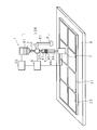
- FIG. 3 is a schematic view of the liquid crystal dropping device 1 and the mother glass substrate 31 according to the embodiment of the present invention
- FIG. 4 is a schematic enlarged view showing the configuration of the liquid crystal dropping device 1.
- a stage 9 is disposed in a predetermined liquid crystal dropping area, and a mother glass substrate 31 including eight color filter substrates 23 is disposed on the stage 9.
- the liquid crystal dropping device 1 is arranged on the mother glass substrate 31, the liquid crystal dropping device 1 is arranged.
- the liquid crystal dropping area has an atmospheric pressure atmosphere.
- the liquid crystal dropping device 1 includes a liquid crystal bottle 2, a three-way valve 3, a liquid crystal discharge unit 4, a nozzle 5, and a driving means 7.
- the liquid crystal bottle 2 has a tapered lower end and accommodates a liquid crystal material 61.
- the lower end of the liquid crystal bottle 2 is connected to one end of the flow pipe 24, and the other end of the flow pipe 24 is connected to the three-way valve 3.
- One end of the flow pipe 25 is connected to the three-way valve 3, and the other end of the flow pipe 25 is connected to the liquid crystal discharge section 4.
- the liquid crystal discharge unit 4 is made of glass, for example, and includes a syringe 41 having a bottomed cylindrical shape and a plunger 44 disposed in the syringe 41.
- the plunger 44 is made of, for example, a fluorine-based resin such as polytetrafluoroethylene, and has substantially the same diameter as the inner diameter of the syringe 41.
- the plunger 44 slides inside the syringe 41, has a rod shape, and slides at one end.
- the liquid crystal bottle 2, the three-way valve 3, the liquid crystal discharge unit 4, and the nozzle 5 constitute a drip head 26.
- the dropping head 26 and the driving means 7 are configured to move on the mother glass substrate 31 by the moving means 32.
- the driving means 7 is composed of, for example, a stepping motor or the like that controls the pushing amount (displacement amount) of the sliding portion 42 by the rotation amount.
- the flow pipe 51 has one end connected to the three-way valve 3 and the other end connected to the nozzle 5.
- the nozzle 5 is preferably coated with, for example, polytetrafluoroethylene, since it is easier to cut liquid crystal droplets when the water repellency is increased.
- it depends on the specific gravity, viscosity, surface tension, affinity with the nozzle 5 or water repellency of the liquid crystal material 61.
- the nozzle diameter is designed, and the inner diameter of the syringe 41 is designed.
- a dropping head 26 is prepared for each liquid crystal material 61.
- FIG. 5 is a block diagram showing the operation control unit 8.
- the operation control unit 8 includes a CPU (Central Processing Unit) 81, a ROM (Read Only Memory) 82, a RAM (Random Access Memory) 83, an input / output interface (I / O) 84, and a rewritable nonvolatile memory 85. Connected with a shared bus.
- the CPU 81 reads the control program stored in the ROM 82 into the RAM 83 and executes it.
- the non-volatile memory 85 includes, for example, an EEPROM (ElectricallyrErasablerasProgrammable Read Only Memory) EP or an EPROM (Erasable Programmable Read Only Memory), and the like.
- EEPROM ElectricallyrErasablerasProgrammable Read Only Memory
- EPROM Erasable Programmable Read Only Memory
- a drop condition table or the like associated with the drop conditions is stored in advance.
- the moving means 32, the operation panel 33, the driving means 7, and the three-way valve 3 are connected to the I / O 84.
- the operation panel 33 is operated by a user, such as a power switch, a start switch for instructing operation start, a switch for instructing operation stop, a switch for instructing a weighing operation to be described later, and a switch for instructing second driving to be described later.
- a user such as a power switch, a start switch for instructing operation start, a switch for instructing operation stop, a switch for instructing a weighing operation to be described later, and a switch for instructing second driving to be described later.
- Various switches are provided.
- the display panel 30 is manufactured by the method for manufacturing the display module 91 of the present invention, first, for example, eight TFT substrates 10 are formed on a mother glass substrate (not shown), and for example, eight substrates are formed on another mother glass substrate 31.
- the color filter substrate 23 is formed.
- an ultraviolet curable resin, or an ultraviolet curable resin and a thermosetting resin are used as a sealing material, and a frame-shaped seal pattern is formed by a dispenser on the image display area of the mother glass substrate 31 of the color filter substrate 23, and is dropped and bonded.
- the mother glass substrate of the TFT substrate 10 is bonded to the mother glass substrate 31 to cure the seal.
- the TFT substrate 10 and the color filter substrate 23 are cut out from the two bonded mother glass substrates in a bonded state, and the display panel 30 is obtained through various processes.
- the dropping head 26 When the liquid crystal material 61 is dropped on the mother glass substrate 31, first, the dropping head 26 is moved to a predetermined position on the color filter substrate 23 on the mother glass substrate 31 by the moving means 32 based on the control of the operation control unit 8. Then, the flow tube 24 and the flow tube 25 side of the three-way valve 3 is opened, and the plunger 44 is lowered by the driving means 7 to send a predetermined amount of the liquid crystal material 61 to the syringe 41. Next, the flow pipe 25 and flow pipe 51 side of the three-way valve 3 is opened, the plunger 44 is raised by the driving means 7 to send the liquid crystal material 61 to the nozzle 5, and the liquid crystal material 61 is fed from the nozzle 5 to the color filter substrate 23. Dripping.
- the operation control unit 8 moves the dropping head 26 to a plurality of positions on the color filter substrate 23 by the moving unit 32 and drops the liquid crystal material 61. This is repeated for each color filter substrate 23.
- the drive by this operation control part 8 is called 1st drive
- the mother glass substrate 31 corresponds to the model of the display module 91, and the dropping condition is switched for each model of the display module 91 as described above.
- the liquid crystal material 61 is continuously dropped onto the mother glass substrate 31 for the display module 91 of the same model, the liquid crystal material 61 is continuously supplied to the syringe 41 and the plunger 44 is continuously moved up and down with a stroke of about 50 mm. Therefore, the problem of sticking of the sliding portion 42 does not occur.
- the dropping head 26 is removed from the driving means 7 and replaced with the dropping head 26 for the next model, and the liquid crystal material 61 is switched. Then, in order to confirm whether or not the liquid crystal material 61 can be dropped normally for the next model, a weighing operation for weighing the dropped amount of the liquid crystal material 61 is performed.
- the plunger 44 does not slide until the dropping process of the liquid crystal material 61 is started after the model switching operation, and the above-described problem of the fixing of the sliding portion 42 has occurred.
- the operation control unit 8 moves the plunger 44 to a reciprocating distance (for example, 0. 0 mm) shorter than the stroke until the dropping process of the liquid crystal material 61 is started for the production of the next model. Second driving is performed by sliding at 1 to 0.2 mm.
- FIG. 6 is a flowchart showing the procedure of the first drive and the second drive by the operation control unit 8.
- the CPU 81 of the operation control unit 8 determines whether or not an instruction to start dropping the liquid crystal material 61 has been received (S1). When the CPU 81 determines that the instruction has not been received (S1: NO), the determination process is repeated. When the CPU 81 determines that the instruction has been received (S1: YES), the CPU 81 performs the first drive (S2).
- the CPU 81 moves the dropping head 26 to a predetermined position for each color filter substrate 23 by the moving means 32, moves the plunger 44 up and down, and drops the liquid crystal material 61 onto the color filter substrate 23.
- the CPU 81 determines whether or not the dropping is finished (S3). When the CPU 81 determines that the dropping has not ended (S3: NO), the CPU repeats the determination process. When the CPU 81 determines that the dripping has been completed (S3: YES), it determines whether or not an instruction for switching the model has been received (S4). If the CPU 81 determines that it has not received an instruction to switch models (S4: NO), it returns the process to step S1. When the model switching is not performed, the liquid crystal material 61 is continuously dropped on the color filter substrate 23 of the same model, and the reciprocating motion of the sliding portion 42 in the syringe 41 is continued. There is no problem.
- the CPU 81 determines that an instruction for switching the model has been received (S4: YES), it reads out the dropping condition table from the nonvolatile memory 85, performs a model switching operation such as a weighing operation (S5), and whether or not the model switching is completed. Is determined (S6). When the CPU 81 determines that the model switching has not been completed (S6: NO), the determination process is repeated.
- the CPU 81 determines whether or not an instruction for the second drive has been received (S7). When the CPU 81 determines that the second drive instruction has not been received (S7: NO), this determination process is repeated.
- the CPU 81 determines that the instruction for the second drive has been received (S7: YES)
- the CPU 81 performs the second drive for sliding the plunger 44 at a reciprocation distance shorter than the dropping stroke of the liquid crystal material 61 (S8).
- CPU81 determines whether or not an instruction to stop the second drive has been received (S9). When it is determined that the CPU 81 has not received an instruction to stop the second drive (S9: NO), this determination process is repeated.
- step S1 If the CPU 81 determines that an instruction to stop the second drive has been received (S9: YES), it stops the second drive and ends the process.
- an instruction to drop the liquid crystal material 61 onto the color filter substrate 23 of the switched model is received, the process of step S1 is performed and the following steps are repeated.
- the sliding portion 42 is fixed to the inner wall of the syringe 41, and the liquid crystal material When the dropping process 61 is performed, the liquid material 61 is reliably prevented from being peeled off and mixed into the liquid crystal material 61.
- the syringe 41 is made of glass and the plunger 44 is made of a fluororesin, the sticking of the sliding portion 42 is suppressed.
- pressure loss does not arise and dropping precision is favorable. Therefore, the occurrence of display defects such as bright spot defects in the display module 91 is suppressed, and the display quality and yield are good.
- the embodiment disclosed this time should be considered as illustrative in all points and not restrictive.
- the scope of the present invention is not intended to include the above-described meanings, but is intended to include meanings equivalent to the claims and all modifications within the scope of the claims.
- the liquid crystal display device is not limited to the display module 91 of the TV receiver 90.
Landscapes
- Physics & Mathematics (AREA)
- Nonlinear Science (AREA)
- Chemical & Material Sciences (AREA)
- Crystallography & Structural Chemistry (AREA)
- General Physics & Mathematics (AREA)
- Optics & Photonics (AREA)
- Mathematical Physics (AREA)
- Engineering & Computer Science (AREA)
- Microelectronics & Electronic Packaging (AREA)
- Manufacturing & Machinery (AREA)
- Liquid Crystal (AREA)
Abstract
Description
滴下貼り合わせ法とは、シールパターンに開口部を設けずに、重ね合わせる前の一方の基板(TFT基板又はカラーフィルタ基板)のマザーガラス基板のシールパターンの枠内に液晶を滴下し、その後、減圧下で他方の基板を重ね合わせて貼り付ける方法をいう。この滴下貼り合わせ法によれば、液晶のタクトタイムを飛躍的に短縮することができるという利点がある。
シリンジ及びプランジャを基板に対応して切り替えた後、次の基板への液晶の滴下を開始するまでの間、プランジャは停止しているので、合成樹脂製のプランジャの先端部がシリンジの内壁と接触しており、該先端部が該内壁で固着することがある。この状態で液晶滴下のためにプランジャが動作した場合、前記先端部とシリンジ内壁の抵抗が高いため、固着した合成樹脂が剥がれて発塵し、表示パネルに異物が混入することがある。
異物が混入した場合、明るい点が視認される不良(明点不良)等の表示不良が発生し、表示品位及び歩留まりが低下するという問題がある。
液晶滴下装置71は、液晶瓶2、三方弁3、液晶吐出部4、ノズル5、及び駆動手段7を備える。液晶瓶2に液晶材61が収容される。液晶瓶2の下端部は通流管24の一端部に接続され、通流管24の他端部は三方弁3に接続されている。通流管25の一端部は三方弁3に接続され、通流管25の他端部は液晶吐出部4に接続されている。
そして、特許文献1の液晶滴下装置71のようにフィルタ28により異物を除去するものではなく、追加の部品を必要とせず、フィルタ28による圧力損失が生じず、滴下精度が良好である。
従って、フィルタを有する場合のように圧力損失が生じず、滴下精度が良好であるとともに、液晶表示装置に明点不良等の表示不良が発生するのが抑制され、表示品位及び歩留まりが良好である。
図1は、本発明に係る液晶表示装置(表示モジュール91)を備えるTV受信機90を示す概略斜視図、図2は表示モジュール91が有する表示パネル30を示す概略断面図である。
表示モジュール91は、前後に縦姿勢で配置された前キャビネット92及び後キャビネット93に縦姿勢で収容されている。前キャビネット92は表示モジュール91の周縁部を覆う矩形状の枠体であり、後キャビネット93は、前側が開放された矩形のトレイ状をなす。
基板11上にゲート配線12が形成され、基板11及びゲート配線12を覆うように絶縁膜13が形成されている。絶縁膜13上に複数の画素電極14が形成され、該画素電極14を覆うように透明の配向膜16が形成されている。画素電極14はアクティブマトリクスとともに形成され、図2においてはアクティブマトリクスのゲート配線12を示している。基板11、ゲート配線12、絶縁膜13、及び画素電極14からTFT基板10が構成される。
そして、液晶層6を狭持するように配向膜16,20が貼り合わせられて基板11,17が固定され、基板11,17の外側に偏光板21,22が設けられている。
液晶瓶2、三方弁3、液晶吐出部4、及びノズル5から滴下ヘッド26が構成される。
滴下ヘッド26及び駆動手段7は、移動手段32によりマザーガラス基板31上を移動するように構成されている。
通流管51は、一端部が三方弁3に接続され、他端部がノズル5に接続されている。ノズル5は、撥水性を高めた方が液晶滴を切りやすいので、例えばポリテトラフルオロエチレンによるコーティング加工がされているのが好ましい。プランジャ44の押し出し量に対してノズル5の先端に形成される液晶滴の大きさを最適化するために、液晶材61の比重、粘性、表面張力、ノズル5との親和性又は撥水性に応じてノズル径が設計され、シリンジ41の内径が設計されている。
液晶材61毎に滴下ヘッド26が用意されている。
図5は、運転制御部8を示すブロック図である。
運転制御部8は、CPU(Central Processing Unit)81、ROM(Read Only Memory)82、RAM(Random Access Memory )83、入出力インタフェイス(I/O)84、及び書換可能な不揮発性メモリ85を共有バスで接続してなる。CPU81は、ROM82に記憶した制御プログラムをRAM83に読出して実行する。
同一機種の表示モジュール91用のマザーガラス基板31に連続して液晶材61を滴下する場合、シリンジ41へ連続して液晶材61が供給され、プランジャ44が略50mmのストロークで連続して昇降するので、摺動部42の固着の問題は生じない。
この機種切替作業の後、液晶材61の滴下処理を開始するまで、プランジャ44は摺動しないので、上述の摺動部42の固着の問題が生じていた。本発明においては、機種切替作業の後、次の機種の生産のために液晶材61の滴下処理を開始するまで、運転制御部8はプランジャ44を、前記ストロークより短い往復動距離(例えば0.1~0.2mm)で摺動させる第2駆動を行う。
図6は、運転制御部8による第1駆動及び第2駆動の処理の手順を示すフローチャートである。
運転制御部8のCPU81は、まず、液晶材61の滴下の開始の指示を受け付けたか否かを判定する(S1)。CPU81は前記指示を受け付けていないと判定した場合(S1:NO)、この判定の処理を繰り返す。
CPU81は前記指示を受け付けたと判定した場合(S1:YES)、第1駆動を行う(S2)。CPU81は、移動手段32によりカラーフィルタ基板23毎に所定の位置に滴下ヘッド26を移動させ、プランジャ44を昇降させ、液晶材61をカラーフィルタ基板23に滴下させる。
CPU81は滴下が終了したと判定した場合(S3:YES)、機種切替の指示を受け付けたか否かを判定する(S4)。CPU81は機種切替の指示を受け付けていないと判定した場合(S4:NO)、処理をステップS1へ戻す。機種切替を行わない場合、同一機種のカラーフィルタ基板23に対する液晶材61の滴下が引き続き行われることになり、摺動部42のシリンジ41内での往復動は継続し、シリンジ41への固着の問題は生じない。
切り替えた機種のカラーフィルタ基板23への液晶材61の滴下の指示を受け付けた場合、ステップS1の処理を行い、以下のステップを繰り返す。
従って、表示モジュール91に明点不良等の表示不良が発生するのが抑制されており、表示品位及び歩留まりが良好である。
例えば、本実施の形態においては、カラーフィルタ基板23上に液晶材61を滴下する場合につき説明しているが、これに限定されるものではなく、TFT基板10に液晶材61を滴下することにしてもよい。
さらに、液晶表示装置はTV受信機90の表示モジュール91に限定されるものではない。
2 液晶瓶
24、25 通流管
26 滴下ヘッド
3 三方弁
4 液晶吐出部
41 シリンジ
42 摺動部
43 支持部
44 プランジャ
5 ノズル
51 通流管
6 液晶層
61 液晶材
10 TFT基板
11、17 基板
12 ゲート配線
13 絶縁膜
14 画素電極
16、20 配向膜
18 カラーフィルタ
19 共通電極
21、22 偏光板
23 カラーフィルタ基板
90 TV受信機
91 表示モジュール
92 前キャビネット
93 後キャビネット
94 チューナ
95 デコーダ
96 スタンド
Claims (3)
- 液晶を封入するシリンジと、該シリンジ内を往復動するプランジャと、該プランジャを駆動する駆動手段とを備え、基板上に前記液晶を滴下するように構成されている液晶滴下装置において、
前記基板上に前記液晶を滴下する前に、前記液晶を滴下する場合のストロークより短い往復動距離で、前記駆動手段により前記プランジャを往復動させる手段を有することを特徴とする液晶滴下装置。 - 前記シリンジは、ガラスからなり、
前記プランジャの先端部は、フッ素系樹脂からなることを特徴とする請求項1に記載の液晶滴下装置。 - 液晶を封入するシリンジ、該シリンジ内を往復動するプランジャ、及び該プランジャを駆動する駆動手段を備える液晶滴下装置を用いて、液晶を一の基板の表面に滴下する滴下ステップ、及び前記基板の表面の一部に他の基板を貼り合わせるステップを有する液晶表示装置の製造方法において、
前記一の基板に対応して前記シリンジ及び前記プランジャを切り替えた場合に、切り替えた後、前記滴下ステップの前に、前記駆動手段により前記プランジャを往復動させるステップを有することを特徴とする液晶表示装置の製造方法。
Priority Applications (4)
| Application Number | Priority Date | Filing Date | Title |
|---|---|---|---|
| PCT/JP2014/051318 WO2015111162A1 (ja) | 2014-01-23 | 2014-01-23 | 液晶滴下装置、及び液晶表示装置の製造方法 |
| JP2015558643A JP5945081B2 (ja) | 2014-01-23 | 2014-01-23 | 液晶滴下装置、及び液晶表示装置の製造方法 |
| US15/110,083 US9772524B2 (en) | 2014-01-23 | 2014-01-23 | Liquid crystal dropping device and method of manufacturing liquid crystal display apparatus |
| CN201480073628.2A CN105934705B (zh) | 2014-01-23 | 2014-01-23 | 液晶滴下装置、液晶显示装置制造方法 |
Applications Claiming Priority (1)
| Application Number | Priority Date | Filing Date | Title |
|---|---|---|---|
| PCT/JP2014/051318 WO2015111162A1 (ja) | 2014-01-23 | 2014-01-23 | 液晶滴下装置、及び液晶表示装置の製造方法 |
Publications (1)
| Publication Number | Publication Date |
|---|---|
| WO2015111162A1 true WO2015111162A1 (ja) | 2015-07-30 |
Family
ID=53680993
Family Applications (1)
| Application Number | Title | Priority Date | Filing Date |
|---|---|---|---|
| PCT/JP2014/051318 Ceased WO2015111162A1 (ja) | 2014-01-23 | 2014-01-23 | 液晶滴下装置、及び液晶表示装置の製造方法 |
Country Status (4)
| Country | Link |
|---|---|
| US (1) | US9772524B2 (ja) |
| JP (1) | JP5945081B2 (ja) |
| CN (1) | CN105934705B (ja) |
| WO (1) | WO2015111162A1 (ja) |
Families Citing this family (1)
| Publication number | Priority date | Publication date | Assignee | Title |
|---|---|---|---|---|
| JP2017021241A (ja) * | 2015-07-13 | 2017-01-26 | 株式会社ジャパンディスプレイ | 液晶材料の処理装置および処理方法、液晶表示パネルの製造方法、並びに液晶表示装置 |
Citations (3)
| Publication number | Priority date | Publication date | Assignee | Title |
|---|---|---|---|---|
| JP2005148754A (ja) * | 2003-11-17 | 2005-06-09 | Lg Phillips Lcd Co Ltd | 液晶滴下装置及び液晶滴下方法 |
| JP2006133251A (ja) * | 2004-11-02 | 2006-05-25 | Nec Lcd Technologies Ltd | 液晶表示パネルの製造方法及び液晶滴下装置 |
| JP2008284441A (ja) * | 2007-05-16 | 2008-11-27 | Ulvac Japan Ltd | 液剤滴下装置 |
Family Cites Families (11)
| Publication number | Priority date | Publication date | Assignee | Title |
|---|---|---|---|---|
| US2607342A (en) * | 1950-11-24 | 1952-08-19 | Martin S Abel | Syringe |
| US3150801A (en) * | 1960-09-06 | 1964-09-29 | Clark H Hamilton | Syringe |
| US4046287A (en) * | 1976-05-10 | 1977-09-06 | Graco Inc. | Automatic metering and dispensing system |
| CN1946487A (zh) | 2004-04-09 | 2007-04-11 | 松下电器产业株式会社 | 粘性流体涂敷装置 |
| WO2005097359A1 (ja) | 2004-04-09 | 2005-10-20 | Matsushita Electric Industrial Co., Ltd. | 粘性流体塗布装置 |
| US20060102877A1 (en) | 2004-11-03 | 2006-05-18 | Jin-Sung Kim | System and method for manufacturing a liquid crystal display device |
| KR20060039782A (ko) | 2004-11-03 | 2006-05-09 | 삼성전자주식회사 | 액정 적하 방법 및 액정 적하 장치 |
| JP5340181B2 (ja) * | 2008-02-21 | 2013-11-13 | 武蔵エンジニアリング株式会社 | 液体材料の吐出装置および方法 |
| KR101066602B1 (ko) * | 2009-06-29 | 2011-09-22 | 에이피시스템 주식회사 | 액정 사출용 시린지 및 이를 이용한 액정 사출 장치와 액정 사출 방법 |
| KR101288987B1 (ko) * | 2010-04-30 | 2013-07-23 | 에이피시스템 주식회사 | 토출유닛 및 기판 처리 장치 |
| JP6098807B2 (ja) * | 2012-04-20 | 2017-03-22 | Tdk株式会社 | 塗布ヘッド及び液滴塗布装置 |
-
2014
- 2014-01-23 JP JP2015558643A patent/JP5945081B2/ja not_active Expired - Fee Related
- 2014-01-23 WO PCT/JP2014/051318 patent/WO2015111162A1/ja not_active Ceased
- 2014-01-23 US US15/110,083 patent/US9772524B2/en active Active
- 2014-01-23 CN CN201480073628.2A patent/CN105934705B/zh active Active
Patent Citations (3)
| Publication number | Priority date | Publication date | Assignee | Title |
|---|---|---|---|---|
| JP2005148754A (ja) * | 2003-11-17 | 2005-06-09 | Lg Phillips Lcd Co Ltd | 液晶滴下装置及び液晶滴下方法 |
| JP2006133251A (ja) * | 2004-11-02 | 2006-05-25 | Nec Lcd Technologies Ltd | 液晶表示パネルの製造方法及び液晶滴下装置 |
| JP2008284441A (ja) * | 2007-05-16 | 2008-11-27 | Ulvac Japan Ltd | 液剤滴下装置 |
Also Published As
| Publication number | Publication date |
|---|---|
| US9772524B2 (en) | 2017-09-26 |
| JPWO2015111162A1 (ja) | 2017-03-23 |
| CN105934705B (zh) | 2018-02-16 |
| CN105934705A (zh) | 2016-09-07 |
| JP5945081B2 (ja) | 2016-07-05 |
| US20160334655A1 (en) | 2016-11-17 |
Similar Documents
| Publication | Publication Date | Title |
|---|---|---|
| US9586238B2 (en) | Needle clean device and sealant coater having the device | |
| JP4847973B2 (ja) | 可撓性基材の貼り合せ工程及びそれに使用する図形化シール材 | |
| JP2002122873A (ja) | 液晶装置の製造方法 | |
| JP2004199076A (ja) | 液晶表示パネルのディスペンサ及びこれを利用したノズルと基板とのギャップ制御方法 | |
| JP4391211B2 (ja) | 液晶表示装置の製造方法及びそれに用いる液晶滴下装置 | |
| JP5945081B2 (ja) | 液晶滴下装置、及び液晶表示装置の製造方法 | |
| JP2008286996A (ja) | 液晶表示装置及びその製造方法 | |
| US20050122464A1 (en) | One-drop fill spacerless process for liquid crystal cell on a silicon backplane or microdisplays | |
| JP2003057666A (ja) | 液晶パネルの製造方法、その製造装置および製造システム | |
| JP2009015131A (ja) | 表示装置の製造方法及び表示装置 | |
| CN1991533A (zh) | 用于液晶显示装置的液晶滴注设备 | |
| US20070089620A1 (en) | Printing apparatus, control method thereof and manufacturing method of flat panel display using the same | |
| US20160211449A1 (en) | Method for manufacturing organic el panel | |
| KR101333972B1 (ko) | 패널의 실런트 디스펜싱 방법 및 이를 이용한 액정표시패널 | |
| JP5358204B2 (ja) | 立体画像表示装置と立体画像表示装置の基板接着方法 | |
| JP2006168794A (ja) | パック体、液滴吐出装置及び電気光学装置並びに電子機器 | |
| US20230382053A1 (en) | Additive Fabrication Techniques with Temperature Compensation | |
| US9841594B2 (en) | Apparatus of coupling substrates for electrowetting display panel and method of coupling substrates for electrowetting display using the same | |
| JP4285194B2 (ja) | 液晶装置の製造方法、液晶装置、電子機器、投射型表示装置 | |
| CN100420985C (zh) | 液晶显示面板的分配器及使用分配器的分配方法 | |
| JP2004361954A (ja) | 液晶表示パネル製造用シリンジ | |
| JP2008286822A (ja) | 液晶表示パネルの製造方法 | |
| KR20060134685A (ko) | 액정표시패널 제조장치와 이를 이용한 액정표시패널의제조방법 | |
| CN104360546B (zh) | 无边框显示装置及其制造方法 | |
| JP2007264242A (ja) | 液晶パネルの製造方法及び液晶パネルの製造装置 |
Legal Events
| Date | Code | Title | Description |
|---|---|---|---|
| 121 | Ep: the epo has been informed by wipo that ep was designated in this application |
Ref document number: 14879375 Country of ref document: EP Kind code of ref document: A1 |
|
| ENP | Entry into the national phase |
Ref document number: 2015558643 Country of ref document: JP Kind code of ref document: A |
|
| WWE | Wipo information: entry into national phase |
Ref document number: 15110083 Country of ref document: US |
|
| NENP | Non-entry into the national phase |
Ref country code: DE |
|
| 122 | Ep: pct application non-entry in european phase |
Ref document number: 14879375 Country of ref document: EP Kind code of ref document: A1 |