WO2015098335A1 - 磁気抵抗効果素子の制御方法および磁気抵抗効果素子の制御装置 - Google Patents
磁気抵抗効果素子の制御方法および磁気抵抗効果素子の制御装置 Download PDFInfo
- Publication number
- WO2015098335A1 WO2015098335A1 PCT/JP2014/080008 JP2014080008W WO2015098335A1 WO 2015098335 A1 WO2015098335 A1 WO 2015098335A1 JP 2014080008 W JP2014080008 W JP 2014080008W WO 2015098335 A1 WO2015098335 A1 WO 2015098335A1
- Authority
- WO
- WIPO (PCT)
- Prior art keywords
- magnetic layer
- voltage
- magnetization
- magnetization direction
- layer
- Prior art date
- Legal status (The legal status is an assumption and is not a legal conclusion. Google has not performed a legal analysis and makes no representation as to the accuracy of the status listed.)
- Ceased
Links
Images




Classifications
-
- G—PHYSICS
- G11—INFORMATION STORAGE
- G11C—STATIC STORES
- G11C11/00—Digital stores characterised by the use of particular electric or magnetic storage elements; Storage elements therefor
- G11C11/02—Digital stores characterised by the use of particular electric or magnetic storage elements; Storage elements therefor using magnetic elements
- G11C11/16—Digital stores characterised by the use of particular electric or magnetic storage elements; Storage elements therefor using magnetic elements using elements in which the storage effect is based on magnetic spin effect
- G11C11/161—Digital stores characterised by the use of particular electric or magnetic storage elements; Storage elements therefor using magnetic elements using elements in which the storage effect is based on magnetic spin effect details concerning the memory cell structure, e.g. the layers of the ferromagnetic memory cell
-
- G—PHYSICS
- G11—INFORMATION STORAGE
- G11C—STATIC STORES
- G11C11/00—Digital stores characterised by the use of particular electric or magnetic storage elements; Storage elements therefor
- G11C11/02—Digital stores characterised by the use of particular electric or magnetic storage elements; Storage elements therefor using magnetic elements
- G11C11/16—Digital stores characterised by the use of particular electric or magnetic storage elements; Storage elements therefor using magnetic elements using elements in which the storage effect is based on magnetic spin effect
- G11C11/165—Auxiliary circuits
- G11C11/1675—Writing or programming circuits or methods
-
- G—PHYSICS
- G11—INFORMATION STORAGE
- G11C—STATIC STORES
- G11C11/00—Digital stores characterised by the use of particular electric or magnetic storage elements; Storage elements therefor
- G11C11/02—Digital stores characterised by the use of particular electric or magnetic storage elements; Storage elements therefor using magnetic elements
- G11C11/16—Digital stores characterised by the use of particular electric or magnetic storage elements; Storage elements therefor using magnetic elements using elements in which the storage effect is based on magnetic spin effect
- G11C11/165—Auxiliary circuits
- G11C11/1693—Timing circuits or methods
Definitions
- the present invention relates to a magnetoresistive effect element control method and a magnetoresistive effect element control apparatus.
- a magnetoresistive effect element having a three-layer structure of a ferromagnetic layer / nonmagnetic layer / ferromagnetic layer changes its resistance depending on the relative directions of magnetization of the two ferromagnetic layers. By making the two states in the case of being nearly parallel correspond to “0” or “1”, respectively, it is used as a magnetic memory cell that records information as the magnetization direction. Information reading is performed by reading the element resistance.
- the nonmagnetic layer may be a metal or an insulator.
- rewriting methods magnetization reversal methods
- an electrical writing method in which a voltage is applied between the ferromagnetic layers is advantageous from the viewpoint of high integration and low power consumption.
- Typical examples of such a writing method include a spin injection magnetization reversal method and an electric field induced magnetization reversal method.
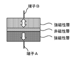
- a current is applied through a three-layer structure of a ferromagnetic layer / nonmagnetic layer / ferromagnetic layer, and magnetization reversal is performed through exchange of angular momentum.
- the magnetization reversal direction can be controlled by the direction of current.
- the lower electrode has a fixed layer whose magnetization is less likely to be reversed than the upper electrode, and the upper electrode is a recording layer, and a positive voltage is applied to terminal B on the recording layer side with respect to terminal A on the fixed layer side.
- the current flows from the recording layer side to the fixed layer side, and the magnetization direction of the recording layer is reversed so as to be parallel to the magnetization direction of the fixed layer.
- a negative voltage is applied to terminal B relative to terminal A, the magnetization direction of the recording layer is reversed so that the magnetization direction of the fixed layer is antiparallel.
- the magnetization reversal direction is determined by the current direction, and the probability of successful information writing improves when a larger current is passed for a longer time. Therefore, in the information writing, the stability of the information writing can be ensured by applying the current for a time longer than the magnetization reversal time predicted to be the minimum necessary.
- the magnetization reversal time of the spin injection magnetization reversal method can be reduced by increasing the amount of current, it is known that the current necessary for writing increases rapidly in the region where the magnetization reversal time is about 1 ns. (For example, see Non-Patent Document 1 or 2).
- the realistic writing time is about several ns to several tens ns.
- the power consumption when rewriting one memory cell once is determined by energy loss due to Joule heat, and is about 1 pJ for a high-performance magnetoresistive memory cell.
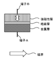
- the electric field induced magnetization reversal method is performed by a capacitor structure element having a three-layer structure of ferromagnetic layer / insulating layer / metal layer as shown in FIG.
- the magnetic anisotropy of the ferromagnetic layer is changed by applying a voltage between the terminal A on the metal layer side and the terminal B on the ferromagnetic layer side, and in the direction indicated by the arrow.
- Generate a magnetic field it is assumed that the direction of the easy axis of the ferromagnetic layer is the vertical direction and the direction parallel to the film surface becomes easy to be magnetized by applying a voltage.
- the voltage is applied to the magnetization having the in-plane easy axis of magnetization.
- Non-Patent Document 3 An arrangement that generates a magnetic field in the direction perpendicular to the surface may be used (for example, see Non-Patent Document 3).
- the magnetization of the ferromagnetic layer can be reversed by precessing around the generated magnetic field, turning off the voltage at about half-period precession, and making the magnetization easy again vertically (for example, Non-Patent Document 4).
- the magnetization reversal time in the electric field induced magnetization reversal method is on the order of several hundred ps to 1 ns.
- the polarity of the applied voltage is the same in both cases of magnetization reversal from parallel to antiparallel state and from antiparallel to parallel state.
- it is necessary to control the voltage amplitude and the application time (voltage pulse length), and the time error allowed when the applied voltage amplitude is fixed is on the order of several tens of ps.
- the power consumed when writing to one memory cell once is charged between the ferromagnetic layer and the metal layer. Is about 1 fJ.
- the write reliability can be improved by extending the write time.
- the write speed is slower and the power consumption is larger than the electric field induced magnetization reversal method. was there.
- the power consumption can be reduced by the method described in Patent Document 1, it is a reduction of about a fraction, and the writing speed is slower and the power consumption is larger than the electric field induced magnetization reversal method.
- the spin injection magnetization reversal method it takes a time from 1 / ns to several ns (dead time) from the application of voltage to the start of magnetization reversal, which is also a factor that cannot increase the writing speed. It has become.
- the writing method using the electric field induced magnetization reversal method is expected to speed up writing several times to several tens of times and reduce power consumption by several hundred times to thousand times compared with the spin injection magnetization reversal method.
- it is necessary to control the voltage application time with an accuracy of several tens of ps, and there is a problem that it is very difficult to control with that accuracy.
- An object of the present invention is to provide a magnetoresistive effect element control method and a magnetoresistive effect element control apparatus.
- the present inventors have faster writing speed than the spin injection magnetization reversal method, low power consumption, and more than the electric field induced magnetization reversal method.
- the inventors have considered that a magnetization reversal method with high controllability can be obtained, and have reached the present invention.
- the magnetoresistive effect element control method includes a magnetoresistive element having a first magnetic layer and a second magnetic layer whose magnetization direction can be easily changed as compared with the first magnetic layer.
- the effect element control method is characterized in that after the electric field induced magnetization reversal method is performed, the magnetization direction of the second magnetic layer is reversed by performing the spin injection magnetization reversal method.
- a control device for a magnetoresistive effect element includes a first magnetic layer and a magnetoresistive effect element having a second magnetic layer whose magnetization direction is easy to change compared to the first magnetic layer. And a control means provided to reverse the magnetization direction of the second magnetic layer by performing the spin injection magnetization reversal method after performing the electric field induced magnetization reversal method.
- the electric field induced magnetization reversal method is used to apply the second magnetic layer before using the spin injection magnetization reversal method.
- the writing speed is faster and the power consumption is lower than when the spin injection magnetization reversal method is used alone.
- the success probability of the magnetization reversal can be increased by the spin injection magnetization reversal method. Therefore, it is not necessary to control the voltage application time with high accuracy. For this reason, control by the electric field induced magnetization reversal method is easy to perform, and a stable magnetization reversal operation with high controllability as a whole can be performed.
- the magnetization reversal is immediately performed by using the electric field induced magnetization reversal method before using the spin injection magnetization reversal method. Can start. For this reason, the dead time generated in the spin transfer magnetization switching method is eliminated, and the writing speed can be increased.
- the method of controlling a magnetoresistive effect element according to the second aspect of the present invention includes a first magnetic layer, a second magnetic layer whose magnetization direction is easily changed compared to the first magnetic layer, and the first magnetic layer.
- a method of controlling a magnetoresistive element having a layer and an insulating layer disposed between the second magnetic layer, wherein the magnetization direction of the second magnetic layer is the magnetization direction of the first magnetic layer The first magnetic layer and the second magnetic layer so as to reverse the magnetization direction by changing the direction of the easy magnetization axis of the second magnetic layer. After the voltage of 1 is applied, the first magnetic layer and the second magnetic layer are arranged between the first magnetic layer and the second magnetic layer so that a current flows from the first magnetic layer toward the second magnetic layer.
- a second voltage having a smaller amplitude than the voltage is applied, and the magnetization direction of the second magnetic layer is the magnetization of the first magnetic layer.
- the third voltage is applied between the first magnetic layer and the second magnetic layer so that a current flows from the second magnetic layer to the first magnetic layer after the third voltage is applied to the first magnetic layer.
- a fourth voltage having a smaller amplitude than the voltage of 3 is applied.
- a magnetoresistive effect element control device comprising: a first magnetic layer; a second magnetic layer whose magnetization direction is easily changed compared to the first magnetic layer; and the first magnetic layer.
- a magnetoresistive element having a layer and an insulating layer disposed between the second magnetic layer, and the magnetization direction of the second magnetic layer is parallel to the magnetization direction of the first magnetic layer.
- a first voltage is applied between the first magnetic layer and the second magnetic layer so as to reverse the magnetization direction by changing the direction of the easy axis of the second magnetic layer. After that, the amplitude is smaller than the first voltage between the first magnetic layer and the second magnetic layer so that a current flows from the first magnetic layer toward the second magnetic layer.
- the magnetization direction of the second magnetic layer is anti-flat with respect to the magnetization direction of the first magnetic layer.
- a third voltage is applied between the first magnetic layer and the second magnetic layer so as to reverse the magnetization direction by changing the direction of the easy axis of the second magnetic layer.
- the amplitude is larger than the third voltage between the first magnetic layer and the second magnetic layer so that a current flows from the second magnetic layer toward the first magnetic layer.
- control means provided to apply a small fourth voltage.
- the first magnetic layer is interposed between the first magnetic layer and the second magnetic layer.
- the voltage 1 or the third voltage By applying the voltage 1 or the third voltage, the direction of the easy magnetization axis of the second magnetic layer is changed, and the second magnetism that precesses around the changed easy magnetization axis.
- the control means in the step of inverting the magnetization direction of the second magnetic layer, includes the first magnetic layer, the second magnetic layer, By applying the first voltage or the third voltage during the period, the direction of the easy axis of the second magnetic layer is changed, and precession is performed around the changed easy axis. It is preferable that the first voltage or the third voltage is switched to the second voltage or the fourth voltage when the magnetization of the second magnetic layer is reversed.
- a magnetoresistive effect element control method and a magnetoresistive effect element control device wherein the second magnetic layer is a recording layer, the magnetization direction of the second magnetic layer is Information can be recorded in the magnetoresistive effect element by rewriting in parallel or antiparallel to the magnetization direction.
- parallel and antiparallel to the magnetization direction of the first magnetic layer are an arrangement that is almost parallel and antiparallel to the magnetization direction of the first magnetic layer. And it is the range of the width
- the magnetization direction of the second magnetic layer is arranged or antiparallel to the magnetization direction of the first magnetic layer.
- the magnetization direction of the second magnetic layer can be reversed using the electric field induced magnetization reversal method. That is, by applying the first voltage or the third voltage between the first magnetic layer and the second magnetic layer, the direction of the easy axis of magnetization of the second magnetic layer can be changed, The magnetization of the second magnetic layer precesses about the changed easy axis.
- the easy axis of the second magnetic layer is returned to the original direction by switching to the second voltage or the fourth voltage having a smaller amplitude than the first voltage or the third voltage. Can return and end precession. As a result, the magnetization direction of the second magnetic layer is in a state of precessing for about a half cycle, and is reversed with respect to the original direction.
- the magnetization direction of the inverted second magnetic layer can be made closer or parallel to the magnetization direction of the first magnetic layer.
- the electric field induced magnetization inversion method is used before the spin injection magnetization inversion method is used. Since the magnetization direction of the magnetic layer is generally reversed, the writing speed is faster and the power consumption is lower than when only the spin injection magnetization reversal method is used. In addition, after reversing the magnetization direction of the second magnetic layer by the electric field induced magnetization reversal method, the success probability of the magnetization reversal can be increased by the spin injection magnetization reversal method. Therefore, it is not necessary to control the voltage application time with high accuracy. For this reason, control by the electric field induced magnetization reversal method is easy to perform, and a stable magnetization reversal operation with high controllability as a whole can be performed.
- the magnetization reversal is immediately performed by using the electric field induced magnetization reversal method before using the spin injection magnetization reversal method. Can start. For this reason, the dead time generated in the spin transfer magnetization switching method is eliminated, and the writing speed can be increased.
- the control means for controlling the applied voltage may have any configuration. For example, by applying a voltage from a DC voltage source through switching controlled by a computer or the like via a transistor, It is preferable that the first to fourth voltages are applied.
- the magnetization direction of the second magnetic layer is larger than 90 degrees from the original direction to 270 degrees, respectively. It is preferable to apply a voltage of a predetermined magnitude or more for a predetermined time so as to rotate within a range of less than the predetermined range.
- the control means may be configured such that the magnetization direction of the second magnetic layer is the original direction as the first voltage and the third voltage, respectively. It is preferable that a voltage of a predetermined magnitude or more is applied for a predetermined time so as to rotate within a range from 90 degrees to less than 270 degrees.
- the first voltage and the third voltage have such a magnitude that the direction of the easy axis of magnetization of the second magnetic layer can be changed, and the precession of magnetization of the second magnetic layer. It preferably has a duration greater than 1 ⁇ 4 period of motion and less than 3 ⁇ 4 period.
- the magnetization direction of the second magnetic layer can be substantially reversed using the electric field induced magnetization reversal method, and the magnetization reversal can be completed with high probability and high speed by the later spin injection magnetization reversal method. it can.
- the magnitudes of the second voltage and the fourth voltage are preferably as large as possible within a range in which the direction of the easy axis of magnetization of the second magnetic layer does not change. In order to improve the probability of successful information writing, a longer duration is preferable, but a shorter one is preferable for higher speed and lower power consumption.
- the first voltage or the third voltage The direction change of the easy axis of the second magnetic layer due to the voltage needs to be greater than 45 degrees and less than 135 degrees.
- the magnetoresistive effect element control method and magnetoresistive effect element control device wherein the first magnetic layer and the second magnetic layer are ferromagnetic metal elements such as Co, Fe, Ni, Mn It is preferable that it is comprised with the material containing at least one.
- the thickness is not limited, but when the easy magnetization direction is determined by the interfacial magnetic anisotropy, the magnetic anisotropy is controlled by voltage, and the film thickness can switch the easy axis direction of magnetization. For example, 0.5 to 2 nm is preferable per CoFeB / MgO junction.
- the insulating layer is preferably made of an oxide such as MgO or AlO, or a material containing at least one of nitrogen and fluorine.
- the insulating layer extends along the thickness direction of the first magnetic layer and the second magnetic layer, It is preferable to arrange between the first magnetic layer and the second magnetic layer. In this case, it is easy to control by applying a voltage between the first magnetic layer and the second magnetic layer.
- the magnetization direction of the first magnetic layer and the second magnetic layer is preferably along the layer thickness direction.
- a magnetoresistive effect element control method comprising: a first magnetic layer; a second magnetic layer whose magnetization direction is easily changed compared to the first magnetic layer; and the first magnetic layer.
- a nonmagnetic layer disposed between a layer and the second magnetic layer, a metal layer disposed opposite to the first magnetic layer with respect to the second magnetic layer, and the second
- a magnetoresistive element having a magnetic layer and an insulating layer disposed between the metal layers, wherein the magnetization direction of the second magnetic layer is the same as the magnetization direction of the first magnetic layer.
- a first voltage is applied between the second magnetic layer and the metal layer so as to reverse the magnetization direction by changing the direction of the easy axis of the second magnetic layer. After the application, the first magnetic layer and the first magnetic layer so that a current flows from the first magnetic layer toward the second magnetic layer.
- a second voltage having a smaller amplitude than the first voltage is applied between the second magnetic layer and the magnetization direction of the second magnetic layer is opposite to the magnetization direction of the first magnetic layer.
- a third voltage was applied between the second magnetic layer and the metal layer so as to reverse the magnetization direction by changing the direction of the easy axis of the second magnetic layer. After that, an amplitude smaller than the third voltage is applied between the first magnetic layer and the second magnetic layer so that a current flows from the second magnetic layer toward the first magnetic layer.
- a voltage of 4 is applied.
- a magnetoresistive effect element control device comprising: a first magnetic layer; a second magnetic layer whose magnetization direction is easily changed compared to the first magnetic layer; and the first magnetic layer.
- a nonmagnetic layer disposed between a layer and the second magnetic layer, a metal layer disposed opposite to the first magnetic layer with respect to the second magnetic layer, and the second
- a magnetoresistive element having an insulating layer disposed between the magnetic layer and the metal layer, and the magnetization direction of the second magnetic layer is parallel to the magnetization direction of the first magnetic layer
- the method for controlling a magnetoresistive effect element wherein in the step of reversing the magnetization direction of the second magnetic layer, the first voltage is applied between the second magnetic layer and the metal layer.
- the third voltage by applying the third voltage, the direction of the easy axis of magnetization of the second magnetic layer is changed, and the magnetization of the second magnetic layer that performs precession about the changed easy axis of magnetization.
- the control means may be arranged between the second magnetic layer and the metal layer in the step of inverting the magnetization direction of the second magnetic layer.
- the first voltage or the third voltage By applying the first voltage or the third voltage, the direction of the easy axis of the second magnetic layer is changed, and the second precession is performed around the changed easy axis. It is preferable that the first voltage or the third voltage is switched to the second voltage or the fourth voltage when the magnetization of the magnetic layer is reversed.
- a magnetoresistive effect element control method and a magnetoresistive effect element control device wherein the second magnetic layer is a recording layer, and the magnetization direction of the second magnetic layer is changed to that of the first magnetic layer.
- Information can be recorded in the magnetoresistive effect element by rewriting in parallel or antiparallel to the magnetization direction.
- parallel and antiparallel to the magnetization direction of the first magnetic layer are an arrangement that is almost parallel and antiparallel to the magnetization direction of the first magnetic layer. And it is the range of the width
- a magnetoresistive effect element control method and magnetoresistive effect element control device wherein the magnetoresistive effect element has a second magnetic layer in common, the first magnetic layer, the nonmagnetic layer,
- the first voltage or the third voltage is applied between the second ferromagnetic layer and the metal layer.
- the electric field induced magnetization reversal method the magnetization direction of the second magnetic layer is reversed, and then the second voltage or the fourth voltage is applied between the first magnetic layer and the second magnetic layer.
- this voltage it is possible to increase the success probability of magnetization reversal and to perform stable magnetization reversal using the spin injection magnetization reversal method.
- the magnetoresistive effect element control method and magnetoresistive effect element control device are the magnetoresistive effect element control method and magnetoresistive effect element control device according to the second aspect of the present invention.
- the magnetization reversal operation can be performed based on the same principle as described above, and the writing speed is higher than that performed only by the spin injection magnetization reversal method.
- the other features and effects are the same as those of the magnetoresistive effect element control method and magnetoresistive effect element control device according to the second aspect of the present invention.
- the first magnetic layer and the second magnetic layer are made of ferromagnetic metal elements such as Co, Fe, Ni, and Mn. It is preferable that it is comprised with the material containing at least one.
- the thickness is not limited, but when the easy magnetization direction is determined by the interfacial magnetic anisotropy, the magnetic anisotropy is controlled by voltage, and the film thickness can switch the easy axis direction of magnetization. For example, 0.5 to 2 nm is preferable per CoFeB / MgO junction. Any material can be used for the nonmagnetic layer.
- the thickness is preferably about 3 nm or more in order to cut the exchange coupling between the first magnetic layer and the second magnetic layer.
- the metal layer is preferably made of a low resistance material such as Au, Cr, Cu, or Al.
- the insulating layer is preferably a material containing one or more oxides such as MgO and AlO, nitrogen and fluorine.
- the thickness of the insulating layer is preferably a film thickness that provides high resistance in order to prevent energy loss due to Joule heat, and is preferably 2 nm or more.
- the nonmagnetic layer is formed along the thickness direction of the first magnetic layer and the second magnetic layer.
- the insulating layer and the metal layer are disposed between the first magnetic layer and the second magnetic layer in a thickness direction of the first magnetic layer and the second magnetic layer.
- the first magnetic layer is preferably stacked on the opposite side of the second magnetic layer. In this case, it is easy to control by applying a voltage between the first magnetic layer and the second magnetic layer and between the second magnetic layer and the metal layer.
- the magnetization direction of the first magnetic layer and the second magnetic layer is preferably along the layer thickness direction.
- a method for controlling a magnetoresistive effect element and a magnetoresistive effect capable of performing a stable magnetization reversal operation with high controllability and at the same time having a higher writing speed and lower power consumption than the spin injection magnetization reversal method can be provided.
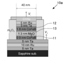
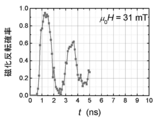
- FIG. 3 It is a longitudinal cross-sectional view which shows the magnetoresistive effect element used with the control method and the control apparatus of a magnetoresistive effect element of embodiment of 1st this invention. It is a longitudinal cross-sectional view of the Example of the magnetoresistive effect element shown in FIG. 3 is a graph showing the voltage application duration dependence of the magnetization reversal probability of a second magnetic layer when a first voltage is applied to the magnetoresistive effect element shown in FIG. 2. 3 is a graph showing the magnetization reversal probability of the second magnetic layer with respect to the second voltage duration t 1 for various durations t E of the first voltage of the magnetoresistive element shown in FIG. FIG.
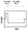
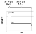
- FIG. 3 shows an applied voltage waveform when the magnetization direction of the second magnetic layer of the magnetoresistive effect element shown in FIG. 1 is rewritten from a state close to parallel to the direction of magnetization of the first magnetic layer to a state close to antiparallel.
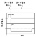
- It is a graph. 1 shows a voltage waveform applied when the magnetization direction of the second magnetic layer of the magnetoresistive effect element shown in FIG. 1 is rewritten from a state close to antiparallel to a state close to parallel to the magnetization direction of the first magnetic layer.
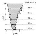
- the magnetoresistive element shown in FIG. 2 is a graph showing when the magnetization reversal probability is 90% or more, the area of the duration t l of the first duration t E and the second voltage of the voltage.
- Terminal B-terminal when the magnetization direction of the second magnetic layer of the magnetoresistive effect element shown in FIG. 8 is rewritten from a state parallel to the magnetization direction of the first magnetic layer to an antiparallel state 6 is a graph showing an applied voltage between C and (b) between a terminal A and a terminal B;
- FIGS. 1 to 7 show a magnetoresistive effect element used in the magnetoresistive effect element control method and magnetoresistive effect element control apparatus according to the first embodiment of the present invention.
- the magnetoresistive effect element 10 includes a first magnetic layer 11, a second magnetic layer 12, and an insulating layer 13.
- the magnetization direction of the first magnetic layer 11 is along the layer thickness direction, and the magnetization direction does not change by 90 ° or more.
- the magnetization direction of the second magnetic layer 12 is along the layer thickness direction, and the second magnetic layer 12 can be changed to an arrangement that is nearly parallel or anti-parallel to the magnetization direction of the first magnetic layer 11.
- the insulating layer 13 is disposed between the first magnetic layer 11 and the second magnetic layer 12 along the thickness direction of the first magnetic layer 11 and the second magnetic layer 12.
- the first magnetic layer 11 is a CoFeB layer having a thickness of 0.9 nm
- the second magnetic layer 12 is a CoFeB layer having a thickness of 1.8 nm
- the insulating layer 13 has a thickness of 1 It consists of a 3 nm MgO layer.
- a Ta layer, a Ru layer, a Ta layer, and a sapphire layer are provided below the first magnetic layer 11 in this order.
- the second magnetic layer 12 has a Ta layer, a Ru layer, and a Cr / Au layer in order from the bottom on the top.
- an AlO protective insulating layer is provided around the joint.
- the magnetoresistive effect element control method and magnetoresistive effect element control device use the second magnetic layer 12 as a recording layer and change the magnetization direction of the second magnetic layer 12 to Information can be recorded in the magnetoresistive effect element 10 by rewriting it to an arrangement that is nearly parallel or anti-parallel to the magnetization direction of one magnetic layer 11.
- a first voltage is applied between the two magnetic layers 12.
- the first voltage has such a magnitude that the direction of the easy axis of magnetization of the second magnetic layer 12 can be changed, so that the effective magnetic field in the direction of the arrow in FIG.
- the direction of the easy axis of magnetization of the second magnetic layer 12 changes from the vertical direction to the in-layer direction substantially perpendicularly.
- the magnetization of the second magnetic layer 12 precesses about the changed easy axis.
- the magnetoresistive element 10 a shown in FIG. 2 when a voltage of 0.7 V is applied as the first voltage between the first magnetic layer 11 and the second magnetic layer 12, the second magnetic layer 12 Since the magnetization precesses, the magnetization reversal probability oscillates with respect to the voltage application duration as shown in FIG. Note that the magnetization reversal probability in FIG. 3 is such that a voltage is applied when the magnetization direction of the second magnetic layer 12 is nearly parallel to the magnetization direction of the first magnetic layer 11, and the second magnetic layer 12 The probability that the magnetization direction is nearly antiparallel to the magnetization direction of the first magnetic layer 11 is shown. In FIG. 3, the applied magnetic field has a magnetic flux density of 31 mT and a duration of up to 5 ns.
- the magnetization direction of the second magnetic layer 12 is in a state of precession of about a half cycle, and is almost reversed with respect to the original direction, that is, in the first magnetic layer 11. It is almost antiparallel to the magnetization direction.
- the magnetization direction of the second magnetic layer 12 can be substantially reversed by using the electric field induced magnetization reversal method.
- the amplitude is smaller than the first voltage so that a current flows from the first magnetic layer 11 to the second magnetic layer 12 between the first magnetic layer 11 and the second magnetic layer 12.
- a second voltage is applied.
- the amplitude of the second voltage is a value at which the easy axis of magnetization of the second magnetic layer 12 does not change, and is preferably applied subsequently to the first voltage.
- FIG. 4 shows the result of obtaining the inversion probability by applying a voltage of 0.5 V as the second voltage to the magnetoresistive effect element 10a shown in FIG.
- FIG. 4 shows the magnetization reversal probability for the duration t 1 of the second voltage of 0.5V for various times from 0 ns to 1.25 ns when the time t E applied with the first voltage of 0.7V. It shows a change.
- the magnetization reversal probability in FIG. 4 is such that a voltage is applied when the magnetization direction of the second magnetic layer 12 is parallel to the magnetization direction of the first magnetic layer 11, and the magnetization direction of the second magnetic layer 12 is The probability of being antiparallel to the magnetization direction of one magnetic layer 11 is shown. As shown in FIG.
- the magnetization direction of the second magnetic layer 12 can be made closer to be antiparallel to the magnetization direction of the first magnetic layer 11. Further, as the duration t E of the first voltage approaches 1.25 ns, which is the time when the magnetization reversal probability becomes the highest as shown in FIG. 3, the magnetization reversal probability due to the second voltage can be increased more quickly.
- the probability of magnetization reversal is increased by increasing t l , so that the torque for directing the magnetization to the antiparallel arrangement (the force acting on the magnetization) is spin injection. It can be seen that In this way, by applying the second voltage subsequent to the first voltage, it is possible to increase the success probability of magnetization reversal and perform stable magnetization reversal using the spin injection magnetization reversal method.
- the entire writing time t E + t 1 is shortened by 8.75 ns or more compared to the case where only spin injection magnetization reversal is used. Can do.
- the magnetoresistive effect element control method and magnetoresistive effect element control device after applying the first voltage of the duration t E as shown in FIG.
- the second voltage of the duration t 1 By applying the second voltage of the duration t 1 , the magnetization direction of the second magnetic layer 12 is changed from a state close to parallel to the direction of magnetization of the first magnetic layer 11 to a state close to antiparallel. Can be rewritten.
- a third voltage is applied between the terminal A and the terminal B, that is, between the first magnetic layer 11 and the second magnetic layer 12.
- the third voltage is preferably the same polarity and the same magnitude as the first voltage.
- the voltage is changed to a value that does not change the easy magnetization axis of the second magnetic layer 12, thereby returning the easy magnetization axis of the second magnetic layer 12 to the original direction.
- the magnetization direction of the second magnetic layer 12 is in a state of precession of about a half cycle, and is almost reversed with respect to the original direction, that is, in the first magnetic layer 11. The state is almost parallel to the magnetization direction.
- the magnetization direction of the second magnetic layer 12 can be substantially reversed by using the electric field induced magnetization reversal method.
- a fourth voltage smaller than the third voltage is set so that a current flows from the second magnetic layer 12 toward the first magnetic layer 11 between the first magnetic layer 11 and the second magnetic layer 12.
- the fourth voltage is a value that does not change the easy axis of magnetization of the second magnetic layer 12, and is preferably applied subsequently to the third voltage.
- the fourth voltage is opposite in polarity to the second voltage.
- the magnetoresistive effect element control method and magnetoresistive effect element control device after applying the third voltage of the duration t E as shown in FIG.
- the fourth voltage of the duration t 1 By applying the fourth voltage of the duration t 1 , the magnetization direction of the second magnetic layer 12 is changed from a state close to antiparallel to a state close to parallel to the magnetization direction of the first magnetic layer 11. Can be rewritten.
- the energy consumption of the spin injection magnetization reversal method is proportional to the writing time, the power consumption can be reduced by increasing the speed.
- the electric field induced magnetization reversal method is used before the spin injection magnetization reversal method is used. Since the magnetization direction of the second magnetic layer 12 is generally reversed, the writing speed is faster and the power consumption is lower than in the case where only the spin injection magnetization reversal method is used. Further, since the probability of successful magnetization reversal can be increased by spin injection magnetization reversal after the magnetization direction of the second magnetic layer 12 is reversed by electric field induced reversal, the electric field induced magnetization reversal is used. There is no need to perform highly accurate magnetization reversal. For this reason, it is easy to perform control by the electric field induced magnetization reversal method, and stable magnetization reversal operation with high controllability as a whole can be performed.
- the electric field induced magnetization inversion method is used immediately before the spin injection magnetization inversion method is used.
- the magnetization reversal can be started. For this reason, the dead time generated in the spin transfer magnetization switching method is eliminated, and the writing speed can be increased.
- the magnetoresistive effect element control method and magnetoresistive effect element control device substantially reverse the magnetization direction of the second magnetic layer 12 by using the electric field induced magnetization reversal method.
- the second magnetic layer 12 is rotated for a time during which the magnetization direction of the second magnetic layer 12 is rotated in the range of more than 90 degrees and less than 270 degrees from the original direction, that is, the second voltage.
- the magnetic layer 12 is preferably applied for a duration longer than 1 ⁇ 4 period and less than 3 ⁇ 4 period of the magnetization precession.
- the magnitudes of the second voltage and the fourth voltage are set so that the second magnetic layer 12 is easily magnetized. It is preferably as large as possible within a range in which the direction of the axis does not change. In order to improve the probability of successful information writing, a longer duration is preferable, but a shorter one is preferable for higher speed and lower power consumption.
- the magnetoresistive effect element 10 is controlled by the control means.
- the magnetoresistive element 20 includes a first magnetic layer 21, a second magnetic layer 22, a nonmagnetic layer 23, a metal layer 24, and an insulating layer 25.
- the magnetization direction of the first magnetic layer 21 is less likely to change than that of the second magnetic layer.
- the second magnetic layer 22 can be easily changed to an arrangement close to parallel or anti-parallel to the magnetization direction of the first magnetic layer 21 compared to the first magnetic layer. It has become.
- the nonmagnetic layer 23 is disposed between the first magnetic layer 21 and the second magnetic layer 22 along the thickness direction of the first magnetic layer 21 and the second magnetic layer 22.
- the metal layer 24 is disposed on the side opposite to the first magnetic layer 21 with respect to the second magnetic layer 22.
- the insulating layer 25 is disposed between the second magnetic layer 22 and the metal layer 24 along the thickness direction of the first magnetic layer 21 and the second magnetic layer 22.
- the magnetoresistive effect element 10 has the first magnetic layer 21, the nonmagnetic layer 23, and the second magnetic layer 22 in common with the second magnetic layer 22, and is based on the spin injection magnetization reversal method shown in FIG.
- the structure is a combination of the structure of the electric field induced magnetization reversal method shown in FIG. 12, which includes the second magnetic layer 22, the insulating layer 25, and the metal layer 24.
- the magnetoresistive effect element control method and magnetoresistive effect element control device use the second magnetic layer 22 as a recording layer and change the magnetization direction of the second magnetic layer 22 to Information can be recorded in the magnetoresistive effect element 20 by rewriting to an arrangement that is nearly parallel or anti-parallel to the magnetization direction of one magnetic layer 21.
- the magnetoresistive effect element control method and magnetoresistive effect element control apparatus are the same as the magnetoresistive effect element control method and magnetoresistive effect element according to the first embodiment of the present invention.
- the magnetization reversal operation can be performed on the same principle as that of the control device. In the following description, descriptions overlapping with the magnetoresistive effect element control method and magnetoresistive effect element control device according to the first embodiment of the present invention are omitted.
- the application of the first voltage is stopped, and the first voltage is applied between the terminal A and the terminal B, that is, between the first magnetic layer 21 and the second magnetic layer 22.
- a second voltage having a small amplitude is applied.
- the magnetization of the inverted second magnetic layer 22 is applied by applying a second voltage so that a current flows from the first magnetic layer 21 toward the second magnetic layer 22 following the first voltage.
- the direction can be made closer to be antiparallel to the magnetization direction of the first magnetic layer 21.
- the magnetoresistive effect element control method and magnetoresistive effect element control device applied the first voltage of the duration t E as shown in FIG. Thereafter, by applying a second voltage of duration t 1 , the magnetization direction of the second magnetic layer 22 is changed from a state close to parallel to the magnetization direction of the first magnetic layer 21 to a state close to anti-parallel. Can be rewritten.
- the direction of the easy axis of magnetization of the second magnetic layer 22 changes from the vertical direction to the direction substantially perpendicular to the in-layer direction, and the changed easy axis of As a center, the magnetization of the second magnetic layer 22 precesses.
- the application of the third voltage is stopped, and the third voltage is applied between the terminal A and the terminal B, that is, between the first magnetic layer 21 and the second magnetic layer 22.
- a fourth voltage having a small amplitude is applied.
- the easy axis of magnetization of the second magnetic layer 22 is returned to the original direction to finish the precession, and the magnetization direction of the second magnetic layer 22 is substantially reversed with respect to the original direction, that is,
- the first magnetic layer 21 can be substantially parallel to the magnetization direction.
- the magnetization of the inverted second magnetic layer 22 is applied by applying a fourth voltage so that a current flows from the second magnetic layer 22 toward the first magnetic layer 21 following the third voltage.
- the direction can be made closer to and parallel to the magnetization direction of the first magnetic layer 21.
- the magnetoresistive effect element control method and magnetoresistive effect element control apparatus applied the third voltage of the duration t E as shown in FIG. Thereafter, by applying a fourth voltage having a duration t 1 , the magnetization direction of the second magnetic layer 22 is changed from a state close to anti-parallel to the direction of magnetization of the first magnetic layer 21 to a state close to parallel. Can be rewritten.
- the magnetoresistive effect element control method and magnetoresistive effect element control device first, between the second ferromagnetic layer and the metal layer 24, the first By applying a voltage or a third voltage, the magnetization direction of the second magnetic layer 22 is reversed using an electric field induced magnetization reversal method, and then the first magnetic layer 21 and the second magnetic layer 22 are reversed.
- the second voltage or the fourth voltage between the two the success rate of magnetization reversal can be increased and stable magnetization reversal can be performed using the spin injection magnetization reversal method. For this reason, the writing speed is faster and the power consumption is lower than when the spin injection magnetization reversal method is used alone.
- the control by the electric field induced magnetization reversal method is easy to perform, and a stable magnetization reversal operation with high controllability as a whole can be performed.
- the magnetoresistive effect element 20 can be used as a magnetoresistive effect element while greatly reducing the power consumption in the electric field induced magnetization reversal method by adjusting the resistance of the insulating layer 25 to a sufficiently high resistance. The function can be maintained, and the effect of reducing power consumption is greater than that of the magnetoresistive element 10.
- the magnetoresistive effect element 20 is controlled by the control means.
Landscapes
- Engineering & Computer Science (AREA)
- Computer Hardware Design (AREA)
- Hall/Mr Elements (AREA)
- Mram Or Spin Memory Techniques (AREA)
Abstract
Description
図1乃至図7は、第1の本発明の実施の形態の磁気抵抗効果素子の制御方法および磁気抵抗効果素子の制御装置で使用する磁気抵抗効果素子を示している。
図1に示すように、この磁気抵抗効果素子10は、第1の磁性層11と第2の磁性層12と絶縁層13とを有している。
図8に示すように、この磁気抵抗効果素子20は、第1の磁性層21と第2の磁性層22と非磁性層23と金属層24と絶縁層25とを有している。
11 第1の磁性層
12 第2の磁性層
13 絶縁層
20 磁気抵抗効果素子
21 第1の磁性層
22 第2の磁性層
23 非磁性層
24 金属層
25 絶縁層
Claims (14)
- 第1の磁性層と、磁化方向が前記第1の磁性層と比べて変化させやすい第2の磁性層と、前記第1の磁性層と前記第2の磁性層との間に配置された絶縁層とを有する磁気抵抗効果素子の制御方法であって、
前記第2の磁性層の磁化方向が前記第1の磁性層の磁化方向に対して平行であるとき、前記第2の磁性層の磁化容易軸の方向を変化させることにより磁化方向を反転させるよう、前記第1の磁性層と前記第2の磁性層との間に第1の電圧を印加した後、前記第1の磁性層から前記第2の磁性層に向かって電流が流れるよう、前記第1の磁性層と前記第2の磁性層との間に前記第1の電圧より振幅が小さい第2の電圧を印加し、
前記第2の磁性層の磁化方向が前記第1の磁性層の磁化方向に対して反平行であるとき、前記第2の磁性層の磁化容易軸の方向を変化させることにより磁化方向を反転させるよう、前記第1の磁性層と前記第2の磁性層との間に第3の電圧を印加した後、前記第2の磁性層から前記第1の磁性層に向かって電流が流れるよう、前記第1の磁性層と前記第2の磁性層との間に前記第3の電圧より振幅が小さい第4の電圧を印加することを、
特徴とする磁気抵抗効果素子の制御方法。 - 前記第2の磁性層の磁化方向を反転させる工程において、前記第1の磁性層と前記第2の磁性層との間に前記第1の電圧または前記第3の電圧を印加することにより、前記第2の磁性層の磁化容易軸の方向を変化させ、その変化した磁化容易軸を中心として歳差運動を行う前記第2の磁性層の磁化が反転したとき、前記第1の電圧または前記第3の電圧を、前記第2の電圧または前記第4の電圧に切り替えることを特徴とする請求項1記載の磁気抵抗効果素子の制御方法。
- 前記第1の電圧および前記第3の電圧として、それぞれ前記第2の磁性層の磁化方向が元の方向から90度より大きく270度未満の範囲で回転するよう、所定の大きさ以上の電圧を所定の時間印加することを特徴とする請求項1または2記載の磁気抵抗効果素子の制御方法。
- 第1の磁性層と、磁化方向が前記第1の磁性層と比べて変化させやすい第2の磁性層と、前記第1の磁性層と前記第2の磁性層との間に配置された非磁性層と、前記第2の磁性層に対して前記第1の磁性層とは反対側に配置された金属層と、前記第2の磁性層と前記金属層との間に配置された絶縁層とを有する磁気抵抗効果素子の制御方法であって、
前記第2の磁性層の磁化方向が前記第1の磁性層の磁化方向に対して平行であるとき、前記第2の磁性層の磁化容易軸の方向を変化させることにより磁化方向を反転させるよう、前記第2の磁性層と前記金属層との間に第1の電圧を印加した後、前記第1の磁性層から前記第2の磁性層に向かって電流が流れるよう、前記第1の磁性層と前記第2の磁性層との間に前記第1の電圧より振幅が小さい第2の電圧を印加し、
前記第2の磁性層の磁化方向が前記第1の磁性層の磁化方向に対して反平行であるとき、前記第2の磁性層の磁化容易軸の方向を変化させることにより磁化方向を反転させるよう、前記第2の磁性層と前記金属層との間に第3の電圧を印加した後、前記第2の磁性層から前記第1の磁性層に向かって電流が流れるよう、前記第1の磁性層と前記第2の磁性層との間に前記第3の電圧より振幅が小さい第4の電圧を印加することを、
特徴とする磁気抵抗効果素子の制御方法。 - 前記第2の磁性層の磁化方向を反転させる工程において、前記第2の磁性層と前記金属層との間に前記第1の電圧または前記第3の電圧を印加することにより、前記第2の磁性層の磁化容易軸の方向を変化させ、その変化した磁化容易軸を中心として歳差運動を行う前記第2の磁性層の磁化が反転したとき、前記第1の電圧または前記第3の電圧を、前記第2の電圧または前記第4の電圧に切り替えることを特徴とする請求項4記載の磁気抵抗効果素子の制御方法。
- 前記第1の電圧および前記第3の電圧として、それぞれ前記第2の磁性層の磁化方向が元の方向から90度より大きく270度未満の範囲で回転するよう、所定の大きさ以上の電圧を所定の時間印加することを特徴とする請求項4または5記載の磁気抵抗効果素子の制御方法。
- 第1の磁性層と、磁化方向が前記第1の磁性層と比べて変化させやすい第2の磁性層と、前記第1の磁性層と前記第2の磁性層との間に配置された絶縁層とを有する磁気抵抗効果素子と、
前記第2の磁性層の磁化方向が前記第1の磁性層の磁化方向に対して平行であるとき、前記第2の磁性層の磁化容易軸の方向を変化させることにより磁化方向を反転させるよう、前記第1の磁性層と前記第2の磁性層との間に第1の電圧を印加した後、前記第1の磁性層から前記第2の磁性層に向かって電流が流れるよう、前記第1の磁性層と前記第2の磁性層との間に前記第1の電圧より振幅が小さい第2の電圧を印加し、前記第2の磁性層の磁化方向が前記第1の磁性層の磁化方向に対して反平行であるとき、前記第2の磁性層の磁化容易軸の方向を変化させることにより磁化方向を反転させるよう、前記第1の磁性層と前記第2の磁性層との間に第3の電圧を印加した後、前記第2の磁性層から前記第1の磁性層に向かって電流が流れるよう、前記第1の磁性層と前記第2の磁性層との間に前記第3の電圧より振幅が小さい第4の電圧を印加するよう設けられた制御手段とを、
有することを特徴とする磁気抵抗効果素子の制御装置。 - 前記制御手段は、前記第2の磁性層の磁化方向を反転させる工程において、前記第1の磁性層と前記第2の磁性層との間に前記第1の電圧または前記第3の電圧を印加することにより、前記第2の磁性層の磁化容易軸の方向を変化させ、その変化した磁化容易軸を中心として歳差運動を行う前記第2の磁性層の磁化が反転したとき、前記第1の電圧または前記第3の電圧を、前記第2の電圧または前記第4の電圧に切り替えるよう構成されていることを特徴とする請求項7記載の磁気抵抗効果素子の制御装置。
- 前記制御手段は、前記第1の電圧および前記第3の電圧として、それぞれ前記第2の磁性層の磁化方向が元の方向から90度より大きく270度未満の範囲で回転するよう、所定の大きさ以上の電圧を所定の時間印加するよう構成されていることを特徴とする請求項7または8記載の磁気抵抗効果素子の制御装置。
- 第1の磁性層と、磁化方向が前記第1の磁性層と比べて変化させやすい第2の磁性層と、前記第1の磁性層と前記第2の磁性層との間に配置された非磁性層と、前記第2の磁性層に対して前記第1の磁性層とは反対側に配置された金属層と、前記第2の磁性層と前記金属層との間に配置された絶縁層とを有する磁気抵抗効果素子と、
前記第2の磁性層の磁化方向が前記第1の磁性層の磁化方向に対して平行であるとき、前記第2の磁性層の磁化容易軸の方向を変化させることにより磁化方向を反転させるよう、前記第2の磁性層と前記金属層との間に第1の電圧を印加した後、前記第1の磁性層から前記第2の磁性層に向かって電流が流れるよう、前記第1の磁性層と前記第2の磁性層との間に前記第1の電圧より振幅が小さい第2の電圧を印加し、前記第2の磁性層の磁化方向が前記第1の磁性層の磁化方向に対して反平行であるとき、前記第2の磁性層の磁化容易軸の方向を変化させることにより磁化方向を反転させるよう、前記第2の磁性層と前記金属層との間に第3の電圧を印加した後、前記第2の磁性層から前記第1の磁性層に向かって電流が流れるよう、前記第1の磁性層と前記第2の磁性層との間に前記第3の電圧より振幅が小さい第4の電圧を印加するよう設けられた制御手段とを、
有することを特徴とする磁気抵抗効果素子の制御装置。 - 前記制御手段は、前記第2の磁性層の磁化方向を反転させる工程において、前記第2の磁性層と前記金属層との間に前記第1の電圧または前記第3の電圧を印加することにより、前記第2の磁性層の磁化容易軸の方向を変化させ、その変化した磁化容易軸を中心として歳差運動を行う前記第2の磁性層の磁化が反転したとき、前記第1の電圧または前記第3の電圧を、前記第2の電圧または前記第4の電圧に切り替えるよう構成されていることを特徴とする請求項10記載の磁気抵抗効果素子の制御装置。
- 前記制御手段は、前記第1の電圧および前記第3の電圧として、それぞれ前記第2の磁性層の磁化方向が元の方向から90度より大きく270度未満の範囲で回転するよう、所定の大きさ以上の電圧を所定の時間印加するよう構成されていることを特徴とする請求項10または11記載の磁気抵抗効果素子の制御装置。
- 第1の磁性層と、磁化方向が前記第1の磁性層と比べて変化させやすい第2の磁性層とを有する磁気抵抗効果素子の制御方法であって、
電界誘起磁化反転方式を行った後、スピン注入磁化反転方式を行うことにより、前記第2の磁性層の磁化方向を反転させることを
特徴とする磁気抵抗効果素子の制御方法。 - 第1の磁性層と、磁化方向が前記第1の磁性層と比べて変化させやすい第2の磁性層とを有する磁気抵抗効果素子と、
電界誘起磁化反転方式を行った後、スピン注入磁化反転方式を行うことにより、前記第2の磁性層の磁化方向を反転させるよう設けられた制御手段とを、
有することを特徴とする磁気抵抗効果素子の制御装置。
Priority Applications (2)
| Application Number | Priority Date | Filing Date | Title |
|---|---|---|---|
| US15/108,396 US10127957B2 (en) | 2013-12-27 | 2014-11-13 | Control method for magnetoresistance effect element and control device for magnetoresistance effect element |
| JP2015554667A JP6374404B2 (ja) | 2013-12-27 | 2014-11-13 | 磁気抵抗効果素子の制御方法および磁気抵抗効果素子の制御装置 |
Applications Claiming Priority (2)
| Application Number | Priority Date | Filing Date | Title |
|---|---|---|---|
| JP2013272703 | 2013-12-27 | ||
| JP2013-272703 | 2013-12-27 |
Publications (1)
| Publication Number | Publication Date |
|---|---|
| WO2015098335A1 true WO2015098335A1 (ja) | 2015-07-02 |
Family
ID=53478211
Family Applications (1)
| Application Number | Title | Priority Date | Filing Date |
|---|---|---|---|
| PCT/JP2014/080008 Ceased WO2015098335A1 (ja) | 2013-12-27 | 2014-11-13 | 磁気抵抗効果素子の制御方法および磁気抵抗効果素子の制御装置 |
Country Status (3)
| Country | Link |
|---|---|
| US (1) | US10127957B2 (ja) |
| JP (1) | JP6374404B2 (ja) |
| WO (1) | WO2015098335A1 (ja) |
Families Citing this family (2)
| Publication number | Priority date | Publication date | Assignee | Title |
|---|---|---|---|---|
| FR3064395B1 (fr) * | 2017-03-23 | 2021-12-10 | Commissariat Energie Atomique | Procede de formage d'une cellule memoire non volatile, cellule memoire non volatile formee suivant ce procede et dispositif microelectronique comportant des telles cellules memoire |
| US10788547B2 (en) * | 2019-01-17 | 2020-09-29 | Sandisk Technologies Llc | Voltage-controlled interlayer exchange coupling magnetoresistive memory device and method of operating thereof |
Citations (3)
| Publication number | Priority date | Publication date | Assignee | Title |
|---|---|---|---|---|
| JP2007123455A (ja) * | 2005-10-27 | 2007-05-17 | Renesas Technology Corp | 半導体記憶装置 |
| WO2009128485A1 (ja) * | 2008-04-17 | 2009-10-22 | ソニー株式会社 | 磁気メモリ素子の記録方法 |
| JP2010079986A (ja) * | 2008-09-25 | 2010-04-08 | Toshiba Corp | 磁気抵抗効果素子のデータ書き込み方法及び磁気ランダムアクセスメモリ |
Family Cites Families (7)
| Publication number | Priority date | Publication date | Assignee | Title |
|---|---|---|---|---|
| JP3848072B2 (ja) * | 2000-09-29 | 2006-11-22 | 富士通株式会社 | 磁気記録媒体及びこれを用いた磁気記憶装置 |
| DE602006013948D1 (de) | 2006-05-04 | 2010-06-10 | Hitachi Ltd | Magnetspeichervorrichtung |
| WO2011101947A1 (ja) * | 2010-02-16 | 2011-08-25 | 株式会社日立製作所 | 半導体装置 |
| KR101266791B1 (ko) * | 2012-09-21 | 2013-05-27 | 고려대학교 산학협력단 | 면내 전류와 전기장을 이용한 자기메모리 소자 |
| JP5576449B2 (ja) * | 2012-09-26 | 2014-08-20 | 株式会社東芝 | 不揮発性記憶装置 |
| JP2014203931A (ja) * | 2013-04-03 | 2014-10-27 | 株式会社東芝 | 磁気メモリ、スピン素子およびスピンmosトランジスタ |
| US9691458B2 (en) * | 2013-10-18 | 2017-06-27 | Cornell University | Circuits and devices based on spin hall effect to apply a spin transfer torque with a component perpendicular to the plane of magnetic layers |
-
2014
- 2014-11-13 WO PCT/JP2014/080008 patent/WO2015098335A1/ja not_active Ceased
- 2014-11-13 US US15/108,396 patent/US10127957B2/en active Active
- 2014-11-13 JP JP2015554667A patent/JP6374404B2/ja active Active
Patent Citations (3)
| Publication number | Priority date | Publication date | Assignee | Title |
|---|---|---|---|---|
| JP2007123455A (ja) * | 2005-10-27 | 2007-05-17 | Renesas Technology Corp | 半導体記憶装置 |
| WO2009128485A1 (ja) * | 2008-04-17 | 2009-10-22 | ソニー株式会社 | 磁気メモリ素子の記録方法 |
| JP2010079986A (ja) * | 2008-09-25 | 2010-04-08 | Toshiba Corp | 磁気抵抗効果素子のデータ書き込み方法及び磁気ランダムアクセスメモリ |
Also Published As
| Publication number | Publication date |
|---|---|
| JP6374404B2 (ja) | 2018-08-15 |
| US10127957B2 (en) | 2018-11-13 |
| JPWO2015098335A1 (ja) | 2017-03-23 |
| US20160329086A1 (en) | 2016-11-10 |
Similar Documents
| Publication | Publication Date | Title |
|---|---|---|
| US12160998B2 (en) | Magnetic tunnel junction structures and related methods | |
| JP5644198B2 (ja) | 記憶装置 | |
| TW200834575A (en) | Storage element and memory | |
| US20190156875A1 (en) | Magnetic storage element | |
| JP2014116474A (ja) | 磁気抵抗素子 | |
| KR101231288B1 (ko) | 자기 메모리 셀 및 자기 랜덤 액세스 메모리 | |
| JP6553857B2 (ja) | 磁気トンネル接合素子及び磁気ランダムアクセスメモリ | |
| JP6374404B2 (ja) | 磁気抵抗効果素子の制御方法および磁気抵抗効果素子の制御装置 | |
| JP2006092626A (ja) | メモリ及びその記録方法 | |
| Han et al. | Perspectives of electric field controlled switching in perpendicular magnetic random access | |
| US8149613B2 (en) | Resistance variable memory device | |
| US9767874B2 (en) | Memory apparatus and memory device | |
| Wu et al. | High speed mram with voltage control of magnetic anisotropy (vcma) effect | |
| Eason et al. | Bistable perpendicular switching with in-plane spin polarization and without external fields | |
| JP5486048B2 (ja) | 磁気メモリセル及びランダムアクセスメモリ | |
| JP4631372B2 (ja) | メモリ | |
| Yan | Nonlinear Magnetic Dynamics and The Switching Phase Diagrams in Spintronic Devices | |
| Varghani et al. | A graphite based STT-RAM cell with reduction in switching current |
Legal Events
| Date | Code | Title | Description |
|---|---|---|---|
| 121 | Ep: the epo has been informed by wipo that ep was designated in this application |
Ref document number: 14874373 Country of ref document: EP Kind code of ref document: A1 |
|
| ENP | Entry into the national phase |
Ref document number: 2015554667 Country of ref document: JP Kind code of ref document: A |
|
| NENP | Non-entry into the national phase |
Ref country code: DE |
|
| WWE | Wipo information: entry into national phase |
Ref document number: 15108396 Country of ref document: US |
|
| 122 | Ep: pct application non-entry in european phase |
Ref document number: 14874373 Country of ref document: EP Kind code of ref document: A1 |