WO2015087488A1 - 電源装置 - Google Patents
電源装置 Download PDFInfo
- Publication number
- WO2015087488A1 WO2015087488A1 PCT/JP2014/005767 JP2014005767W WO2015087488A1 WO 2015087488 A1 WO2015087488 A1 WO 2015087488A1 JP 2014005767 W JP2014005767 W JP 2014005767W WO 2015087488 A1 WO2015087488 A1 WO 2015087488A1
- Authority
- WO
- WIPO (PCT)
- Prior art keywords
- operational amplifier
- current detection
- circuit
- secondary battery
- input terminal
- Prior art date
- Legal status (The legal status is an assumption and is not a legal conclusion. Google has not performed a legal analysis and makes no representation as to the accuracy of the status listed.)
- Ceased
Links
Images
Classifications
-
- H—ELECTRICITY
- H01—ELECTRIC ELEMENTS
- H01M—PROCESSES OR MEANS, e.g. BATTERIES, FOR THE DIRECT CONVERSION OF CHEMICAL ENERGY INTO ELECTRICAL ENERGY
- H01M10/00—Secondary cells; Manufacture thereof
- H01M10/42—Methods or arrangements for servicing or maintenance of secondary cells or secondary half-cells
- H01M10/44—Methods for charging or discharging
-
- B—PERFORMING OPERATIONS; TRANSPORTING
- B60—VEHICLES IN GENERAL
- B60L—PROPULSION OF ELECTRICALLY-PROPELLED VEHICLES; SUPPLYING ELECTRIC POWER FOR AUXILIARY EQUIPMENT OF ELECTRICALLY-PROPELLED VEHICLES; ELECTRODYNAMIC BRAKE SYSTEMS FOR VEHICLES IN GENERAL; MAGNETIC SUSPENSION OR LEVITATION FOR VEHICLES; MONITORING OPERATING VARIABLES OF ELECTRICALLY-PROPELLED VEHICLES; ELECTRIC SAFETY DEVICES FOR ELECTRICALLY-PROPELLED VEHICLES
- B60L53/00—Methods of charging batteries, specially adapted for electric vehicles; Charging stations or on-board charging equipment therefor; Exchange of energy storage elements in electric vehicles
- B60L53/10—Methods of charging batteries, specially adapted for electric vehicles; Charging stations or on-board charging equipment therefor; Exchange of energy storage elements in electric vehicles characterised by the energy transfer between the charging station and the vehicle
- B60L53/14—Conductive energy transfer
-
- B—PERFORMING OPERATIONS; TRANSPORTING
- B60—VEHICLES IN GENERAL
- B60L—PROPULSION OF ELECTRICALLY-PROPELLED VEHICLES; SUPPLYING ELECTRIC POWER FOR AUXILIARY EQUIPMENT OF ELECTRICALLY-PROPELLED VEHICLES; ELECTRODYNAMIC BRAKE SYSTEMS FOR VEHICLES IN GENERAL; MAGNETIC SUSPENSION OR LEVITATION FOR VEHICLES; MONITORING OPERATING VARIABLES OF ELECTRICALLY-PROPELLED VEHICLES; ELECTRIC SAFETY DEVICES FOR ELECTRICALLY-PROPELLED VEHICLES
- B60L53/00—Methods of charging batteries, specially adapted for electric vehicles; Charging stations or on-board charging equipment therefor; Exchange of energy storage elements in electric vehicles
- B60L53/20—Methods of charging batteries, specially adapted for electric vehicles; Charging stations or on-board charging equipment therefor; Exchange of energy storage elements in electric vehicles characterised by converters located in the vehicle
- B60L53/22—Constructional details or arrangements of charging converters specially adapted for charging electric vehicles
-
- H—ELECTRICITY
- H02—GENERATION; CONVERSION OR DISTRIBUTION OF ELECTRIC POWER
- H02J—ELECTRIC POWER NETWORKS; CIRCUIT ARRANGEMENTS OR SYSTEMS FOR SUPPLYING OR DISTRIBUTING ELECTRIC POWER; SYSTEMS FOR STORING ELECTRIC ENERGY
- H02J7/00—Circuit arrangements for charging or discharging batteries or for supplying loads from batteries
- H02J7/02—Circuit arrangements for charging or discharging batteries or for supplying loads from batteries for charging batteries from AC mains by converters
-
- H—ELECTRICITY
- H03—ELECTRONIC CIRCUITRY
- H03F—AMPLIFIERS
- H03F3/00—Amplifiers with only discharge tubes or only semiconductor devices as amplifying elements
- H03F3/45—Differential amplifiers
- H03F3/45071—Differential amplifiers with semiconductor devices only
- H03F3/45076—Differential amplifiers with semiconductor devices only characterised by the way of implementation of the active amplifying circuit in the differential amplifier
- H03F3/45475—Differential amplifiers with semiconductor devices only characterised by the way of implementation of the active amplifying circuit in the differential amplifier using IC blocks as the active amplifying circuit
-
- B—PERFORMING OPERATIONS; TRANSPORTING
- B60—VEHICLES IN GENERAL
- B60L—PROPULSION OF ELECTRICALLY-PROPELLED VEHICLES; SUPPLYING ELECTRIC POWER FOR AUXILIARY EQUIPMENT OF ELECTRICALLY-PROPELLED VEHICLES; ELECTRODYNAMIC BRAKE SYSTEMS FOR VEHICLES IN GENERAL; MAGNETIC SUSPENSION OR LEVITATION FOR VEHICLES; MONITORING OPERATING VARIABLES OF ELECTRICALLY-PROPELLED VEHICLES; ELECTRIC SAFETY DEVICES FOR ELECTRICALLY-PROPELLED VEHICLES
- B60L2210/00—Converter types
- B60L2210/10—DC to DC converters
-
- B—PERFORMING OPERATIONS; TRANSPORTING
- B60—VEHICLES IN GENERAL
- B60L—PROPULSION OF ELECTRICALLY-PROPELLED VEHICLES; SUPPLYING ELECTRIC POWER FOR AUXILIARY EQUIPMENT OF ELECTRICALLY-PROPELLED VEHICLES; ELECTRODYNAMIC BRAKE SYSTEMS FOR VEHICLES IN GENERAL; MAGNETIC SUSPENSION OR LEVITATION FOR VEHICLES; MONITORING OPERATING VARIABLES OF ELECTRICALLY-PROPELLED VEHICLES; ELECTRIC SAFETY DEVICES FOR ELECTRICALLY-PROPELLED VEHICLES
- B60L2210/00—Converter types
- B60L2210/30—AC to DC converters
-
- B—PERFORMING OPERATIONS; TRANSPORTING
- B60—VEHICLES IN GENERAL
- B60L—PROPULSION OF ELECTRICALLY-PROPELLED VEHICLES; SUPPLYING ELECTRIC POWER FOR AUXILIARY EQUIPMENT OF ELECTRICALLY-PROPELLED VEHICLES; ELECTRODYNAMIC BRAKE SYSTEMS FOR VEHICLES IN GENERAL; MAGNETIC SUSPENSION OR LEVITATION FOR VEHICLES; MONITORING OPERATING VARIABLES OF ELECTRICALLY-PROPELLED VEHICLES; ELECTRIC SAFETY DEVICES FOR ELECTRICALLY-PROPELLED VEHICLES
- B60L2210/00—Converter types
- B60L2210/40—DC to AC converters
-
- H—ELECTRICITY
- H01—ELECTRIC ELEMENTS
- H01M—PROCESSES OR MEANS, e.g. BATTERIES, FOR THE DIRECT CONVERSION OF CHEMICAL ENERGY INTO ELECTRICAL ENERGY
- H01M2220/00—Batteries for particular applications
- H01M2220/20—Batteries in motive systems, e.g. vehicle, ship, plane
-
- H—ELECTRICITY
- H02—GENERATION; CONVERSION OR DISTRIBUTION OF ELECTRIC POWER
- H02J—ELECTRIC POWER NETWORKS; CIRCUIT ARRANGEMENTS OR SYSTEMS FOR SUPPLYING OR DISTRIBUTING ELECTRIC POWER; SYSTEMS FOR STORING ELECTRIC ENERGY
- H02J2105/00—Networks for supplying or distributing electric power characterised by their spatial reach or by the load
- H02J2105/30—Networks for supplying or distributing electric power characterised by their spatial reach or by the load the load networks being external to vehicles, i.e. exchanging power with vehicles
- H02J2105/33—Networks for supplying or distributing electric power characterised by their spatial reach or by the load the load networks being external to vehicles, i.e. exchanging power with vehicles exchanging power with road vehicles
- H02J2105/37—Networks for supplying or distributing electric power characterised by their spatial reach or by the load the load networks being external to vehicles, i.e. exchanging power with vehicles exchanging power with road vehicles exchanging power with electric vehicles [EV] or with hybrid electric vehicles [HEV]
-
- H—ELECTRICITY
- H02—GENERATION; CONVERSION OR DISTRIBUTION OF ELECTRIC POWER
- H02J—ELECTRIC POWER NETWORKS; CIRCUIT ARRANGEMENTS OR SYSTEMS FOR SUPPLYING OR DISTRIBUTING ELECTRIC POWER; SYSTEMS FOR STORING ELECTRIC ENERGY
- H02J2207/00—Details of circuit arrangements for charging or discharging batteries or supplying loads from batteries
- H02J2207/20—Charging or discharging characterised by the power electronics converter
-
- H—ELECTRICITY
- H03—ELECTRONIC CIRCUITRY
- H03F—AMPLIFIERS
- H03F2203/00—Indexing scheme relating to amplifiers with only discharge tubes or only semiconductor devices as amplifying elements covered by H03F3/00
- H03F2203/45—Indexing scheme relating to differential amplifiers
- H03F2203/45514—Indexing scheme relating to differential amplifiers the FBC comprising one or more switched capacitors, and being coupled between the LC and the IC
-
- Y—GENERAL TAGGING OF NEW TECHNOLOGICAL DEVELOPMENTS; GENERAL TAGGING OF CROSS-SECTIONAL TECHNOLOGIES SPANNING OVER SEVERAL SECTIONS OF THE IPC; TECHNICAL SUBJECTS COVERED BY FORMER USPC CROSS-REFERENCE ART COLLECTIONS [XRACs] AND DIGESTS
- Y02—TECHNOLOGIES OR APPLICATIONS FOR MITIGATION OR ADAPTATION AGAINST CLIMATE CHANGE
- Y02E—REDUCTION OF GREENHOUSE GAS [GHG] EMISSIONS, RELATED TO ENERGY GENERATION, TRANSMISSION OR DISTRIBUTION
- Y02E60/00—Enabling technologies; Technologies with a potential or indirect contribution to GHG emissions mitigation
- Y02E60/10—Energy storage using batteries
-
- Y—GENERAL TAGGING OF NEW TECHNOLOGICAL DEVELOPMENTS; GENERAL TAGGING OF CROSS-SECTIONAL TECHNOLOGIES SPANNING OVER SEVERAL SECTIONS OF THE IPC; TECHNICAL SUBJECTS COVERED BY FORMER USPC CROSS-REFERENCE ART COLLECTIONS [XRACs] AND DIGESTS
- Y02—TECHNOLOGIES OR APPLICATIONS FOR MITIGATION OR ADAPTATION AGAINST CLIMATE CHANGE
- Y02T—CLIMATE CHANGE MITIGATION TECHNOLOGIES RELATED TO TRANSPORTATION
- Y02T10/00—Road transport of goods or passengers
- Y02T10/60—Other road transportation technologies with climate change mitigation effect
- Y02T10/70—Energy storage systems for electromobility, e.g. batteries
-
- Y—GENERAL TAGGING OF NEW TECHNOLOGICAL DEVELOPMENTS; GENERAL TAGGING OF CROSS-SECTIONAL TECHNOLOGIES SPANNING OVER SEVERAL SECTIONS OF THE IPC; TECHNICAL SUBJECTS COVERED BY FORMER USPC CROSS-REFERENCE ART COLLECTIONS [XRACs] AND DIGESTS
- Y02—TECHNOLOGIES OR APPLICATIONS FOR MITIGATION OR ADAPTATION AGAINST CLIMATE CHANGE
- Y02T—CLIMATE CHANGE MITIGATION TECHNOLOGIES RELATED TO TRANSPORTATION
- Y02T10/00—Road transport of goods or passengers
- Y02T10/60—Other road transportation technologies with climate change mitigation effect
- Y02T10/7072—Electromobility specific charging systems or methods for batteries, ultracapacitors, supercapacitors or double-layer capacitors
-
- Y—GENERAL TAGGING OF NEW TECHNOLOGICAL DEVELOPMENTS; GENERAL TAGGING OF CROSS-SECTIONAL TECHNOLOGIES SPANNING OVER SEVERAL SECTIONS OF THE IPC; TECHNICAL SUBJECTS COVERED BY FORMER USPC CROSS-REFERENCE ART COLLECTIONS [XRACs] AND DIGESTS
- Y02—TECHNOLOGIES OR APPLICATIONS FOR MITIGATION OR ADAPTATION AGAINST CLIMATE CHANGE
- Y02T—CLIMATE CHANGE MITIGATION TECHNOLOGIES RELATED TO TRANSPORTATION
- Y02T10/00—Road transport of goods or passengers
- Y02T10/60—Other road transportation technologies with climate change mitigation effect
- Y02T10/72—Electric energy management in electromobility
-
- Y—GENERAL TAGGING OF NEW TECHNOLOGICAL DEVELOPMENTS; GENERAL TAGGING OF CROSS-SECTIONAL TECHNOLOGIES SPANNING OVER SEVERAL SECTIONS OF THE IPC; TECHNICAL SUBJECTS COVERED BY FORMER USPC CROSS-REFERENCE ART COLLECTIONS [XRACs] AND DIGESTS
- Y02—TECHNOLOGIES OR APPLICATIONS FOR MITIGATION OR ADAPTATION AGAINST CLIMATE CHANGE
- Y02T—CLIMATE CHANGE MITIGATION TECHNOLOGIES RELATED TO TRANSPORTATION
- Y02T90/00—Enabling technologies or technologies with a potential or indirect contribution to GHG emissions mitigation
- Y02T90/10—Technologies relating to charging of electric vehicles
- Y02T90/14—Plug-in electric vehicles
Definitions
- the present invention relates to a power supply device to be mounted on a vehicle.
- PHV and EV plug-in hybrid vehicles
- PHV and EV electric vehicles
- PHV and EV it is necessary to charge a battery in the vehicle from outside the vehicle with a dedicated charging cable.
- chargers There are two types of chargers: ordinary chargers and quick chargers. Ordinary chargers require more time to charge than quick chargers, but they can be fully charged and equipment installation costs can be kept low. It is assumed to be installed in a place where parking is done for a long time, such as a house, office, or rental parking lot. On the other hand, the quick charger can be charged 80% in a short time, but the equipment introduction cost becomes high. Installation in places where the staying time is short, such as shopping centers, gas stations, and highways SA, is assumed.
- a single-phase AC 200V or 100V commonly used at home is used as a power source for an ordinary charger.
- Three-phase AC 200V is used for the power supply of the quick charger. Since a normal charger uses a single-phase power supply, a large amount of power ripple occurs at a low cost.
- the quick charger uses three-phase alternating current, and therefore has high power transportation efficiency and small power ripple. However, when used in a general household, it is necessary to lay a dedicated line.
- ripple occurs in the charging current.
- the ripple is larger than when three-phase alternating current is used.
- the influence of ripple becomes large, it becomes impossible to detect an accurate current on the secondary battery side. If a large-scale smoothing filter is provided on the output side of the charger, the ripple can be reduced but the cost is increased.
- the present invention has been made in view of such circumstances, and an object of the present invention is to provide a technique for suppressing the influence of ripples at low cost when charging a secondary battery in a vehicle from a commercial power source.
- a power supply device is a power supply device to be mounted in a vehicle, the secondary battery for supplying power to a traveling motor, and the secondary battery
- a current detection element for detecting a current flowing through the low-pass filter, a low-pass filter having a predetermined cutoff frequency characteristic and passing a signal equal to or lower than the cutoff frequency, and obtaining the signal voltage of the current detection element via the low-pass filter
- a current detection circuit that estimates a current value of a current flowing through the secondary battery from the acquired voltage value.
- the low-pass filter is configured to be able to select at least a first cutoff frequency characteristic and a second cutoff frequency characteristic lower than the first cutoff frequency characteristic, and the secondary battery is charged from a power source outside the vehicle. When done, the second cutoff frequency is selected.
- the influence of ripple can be suppressed at low cost.
- FIG. 1 shows the structure of the vehicle carrying the power supply device which concerns on embodiment of this invention.
- FIG. 1 shows the structure of the vehicle carrying the power supply device which concerns on embodiment of this invention.
- FIG. 1 shows the 1st structural example of the current detection circuit which concerns on embodiment.
- FIG. 1 shows the 1st structural example of the current detection circuit which concerns on embodiment.
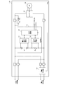
- FIG. 1 is a diagram showing a configuration of a vehicle 100 equipped with a power supply device 10 according to an embodiment of the present invention.
- a plug-in hybrid vehicle (PHV) or an electric vehicle (EV) that can be charged from a commercial power source (system power source) is assumed as the vehicle 100.
- the vehicle 100 includes a power supply device 10, an in-vehicle charger 20, an inverter 30, and a traveling motor 40.
- the power supply device 10 includes a secondary battery E1, a shunt resistor Rs, a voltage detection circuit 11, a current detection circuit 12, and a control circuit 13.
- the secondary battery E ⁇ b> 1 is a secondary battery for storing energy for supplying electric power to the traveling motor 40.
- a nickel metal hydride battery or a lithium ion battery can be used.
- the secondary battery E1 is configured by connecting a plurality of battery cells in series or in series and parallel.
- the secondary battery E1 is charged from a power source installed outside the vehicle 100.
- the charging equipment is roughly classified into a normal charger and a quick charger.
- vehicle 100 a normal charging path for charging secondary battery E1 from the normal charger and a quick charging path for charging secondary battery E1 from the quick charger are separately provided.
- an in-vehicle charger 20 On the normal charging path, an in-vehicle charger 20, a first normal charging switch S5, and a second normal charging switch S6 are provided.
- the in-vehicle charger 20 converts AC power input from an external ordinary charger connected by a charging cable into DC power and outputs the DC power to the secondary battery E1.
- the on-vehicle charger 20 notifies the control circuit 13 of the start and end of normal charging.
- the first normal charging switch S5 is inserted into the wiring between the positive terminal of the in-vehicle charger 20 and the positive terminal of the secondary battery E1, and the second normal charging switch S6 is connected to the negative terminal of the in-vehicle charger 20 and the secondary terminal. It is inserted into the wiring between the negative terminals of the battery E1.
- a relay can be used for the first normal charging switch S5 and the second normal charging switch S6.
- the control circuit 13 controls the first normal charging switch S5 and the second normal charging switch S6 to the on state during normal charging, and the off state at other times.
- a first rapid charge switch S3 and a second rapid charge switch S4 are provided on the rapid charge path.
- the first quick charge switch S3 is inserted into the wiring between the positive terminal of the quick charge plug and the positive terminal of the secondary battery E1
- the second quick charge switch S4 is the negative terminal of the quick charge plug. And inserted into the wiring between the negative terminals of the secondary battery E1.
- a relay can also be used for the first quick charge switch S3 and the second quick charge switch S4.
- the control circuit 13 controls the first quick charge switch S3 and the second quick charge switch S4 to be in an on state at the time of quick charge, and is controlled to be in an off state at other times.
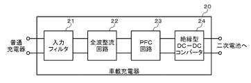
- FIG. 2 is a block diagram illustrating a configuration example of the in-vehicle charger 20.
- the in-vehicle charger 20 includes an input filter 21, a full-wave rectifier circuit 22, a PFC (Power Factor Correction) circuit 23, and an insulated DC-DC converter 24.
- PFC Power Factor Correction
- the input filter 21 passes only the commercial power frequency component from the commercial power AC power supplied from the ordinary charger and outputs it to the full-wave rectifier circuit 22.
- the full-wave rectification circuit 22 performs full-wave rectification on the AC power input from the input filter 21 and outputs it to the PFC circuit 23.
- the full-wave rectifier circuit 22 is configured by, for example, a diode bridge circuit in which four rectifier diodes are connected in a bridge configuration.
- the DC power that has been full-wave rectified by the full-wave rectifier circuit 22 includes ripples.
- the PFC circuit 23 improves the power factor of the DC power input from the full-wave rectifier circuit 22 and outputs the power factor to the isolated DC-DC converter 24.
- the insulated DC-DC converter 24 converts the DC voltage input from the PFC circuit 23 into a set DC voltage and supplies it to the secondary battery E1.
- the insulation type DC-DC converter 24 monitors the output voltage and output current to the secondary battery E1, and performs constant current charging (CC charging) or constant voltage charging (CV charging).
- the isolated DC-DC converter 24 may be a flyback DC-DC converter, a forward DC-DC converter (push-pull DC-DC converter, half-bridge DC-DC converter, full-bridge DC-DC converter), or the like. .
- the inverter 30 converts the DC power supplied from the secondary battery E ⁇ b> 1 into AC power and supplies it to the traveling motor 40 during power running. During regeneration, the AC power supplied from the traveling motor 40 is converted to DC power and supplied to the secondary battery E1.
- the traveling motor 40 may be a large motor capable of self-running, or a small motor that assists in engine traveling (mainly during starting and acceleration). In the EV and strong type PHV, the former large motor is used, and in the small PHV, the latter small motor is used.
- the traveling motor 40 rotates according to the DC power supplied from the inverter 30 during powering. At the time of regeneration, the rotational energy due to deceleration is converted to DC power and supplied to the inverter 30.
- the first main switch S1 is inserted between the path connecting the plus terminal of the secondary battery E1 and the plus terminal of the inverter 30. Further, a series circuit of a precharge switch Sp and a precharge resistor Rp is connected in parallel with the first main switch S1.
- the second main switch S2 is inserted between the path connecting the negative terminal of the secondary battery E1 and the negative terminal of the inverter 30. Relays can be used for the first main switch S1, the second main switch S2, and the precharge switch Sp.
- the control circuit 13 controls the first main switch S1 and the second main switch S2 to be in an on state during traveling, and electrically connects the power supply apparatus 10 and the power system.
- the control circuit 13 controls the first main switch S1 and the second main switch S2 to be in an off state as a rule, and electrically shuts off the power supply device 10 and the power system.
- the traveling motor 40 is started, the control circuit 13 turns on the precharge switch Sp before turning on the first main switch S1 and the second main switch S2.
- a capacitor (not shown) connected in parallel to the inverter 30 can be precharged, and the inrush current when the first main switch S1 and the second main switch S2 are turned on can be suppressed.
- the voltage detection circuit 11 detects the voltage of each battery cell constituting the secondary battery E1.
- the voltage detection circuit 11 outputs the detected voltage value of each battery cell to the control circuit 13.
- the voltage detection circuit 11 is configured by ASIC (Application Specific Integrated Circuit) which is a dedicated custom IC.
- the shunt resistor Rs is connected in series to the negative terminal of the secondary battery E1.
- the shunt resistor Rs is a current detection element for detecting a current flowing through the secondary battery E1.
- a Hall element may be used instead of the shunt resistor Rs.
- the insertion position of the shunt resistor Rs may be any position as long as it is on a path in which a plurality of battery cells are connected in series.
- the current detection circuit 12 detects the value of the current flowing through the secondary battery E1 based on the voltage across the shunt resistor Rs.
- the current detection circuit 12 outputs the detected current value to the control circuit 13.
- the control circuit 13 is composed of a microcomputer and controls the entire power supply device 10. Details of the current detection circuit 12 and the control circuit 13 will be described later.
- a ripple current may be generated according to the power ripple.
- a high-performance quick charger is used, so that sufficient ripple removal capability can be secured.
- a large smoothing capacitor can be installed on the secondary side of the insulated DC-DC converter to increase the ripple removal capability.
- three-phase alternating current is used for the power supply of the quick charger, so that the generated ripple is reduced.
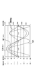
- FIG. 3 is a diagram showing the transition of voltage (AC), current (AC), power, and charging current when charging with a single-phase AC 100 V from a normal charger.
- the charging current (load current) is a fixed value.
- the frequency of the commercial power supply is 50/60 Hz, and 50 Hz is assumed in the following description. Since the voltage (AC) and current (AC) have the same frequency, the frequency of the generated power ripple is twice the commercial frequency. A ripple current having a frequency twice the commercial frequency is also generated in the charging current obtained by dividing the power by the battery voltage.
- the ripple current generated during charging changes regularly because it is determined by the frequency of the commercial power supply.
- the ripple current generated during traveling tends to vary irregularly because it depends on the load during traveling. Therefore, in a hybrid vehicle (HV) that is not charged from a commercial power source, the ripple current rarely adversely affects voltage detection, current detection, and the like.
- the ripple frequency and the sampling frequency match. If the frequencies match, the ripple current will adversely affect current detection.
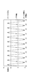
- FIG. 4 is a diagram showing a current flowing through the secondary battery E1 and a sampling cycle.
- FIG. 4 shows an example in which current is sampled at a period of 10 ms. The average value is sampled (see the middle arrow), the worst maximum is sampled (see the upper arrow), and the worst minimum is sampled (lower). (See arrow in). If the average value of the charging current can be sampled, an error does not occur between the actual current value and the detected current value, but an error occurs in the case of sampling other than the average value. The larger the sampling point is, the larger the error.
- the detected current value is used even if it is integrated. For example, the SOC (State Of Charge) of the secondary battery E1 is calculated based on the integrated current value.
- SOC State Of Charge
- the integrated value may cause a large error.
- the sampling frequency is 100 Hz
- a component having a Nyquist frequency of 50 Hz or more becomes a false signal, which is likely to cause a large error.
- components above the Nyquist frequency are removed by a passive anti-aliasing filter composed only of passive elements such as capacitors, coils, and resistors.
- the anti-aliasing filter that sufficiently attenuates the high-frequency component has a large individual difference due to component variation.
- the cutoff frequency of the anti-aliasing filter is slightly lower than the Nyquist frequency.
- the necessary band for current detection depends on the control frequency. For example, when sampling is performed at a cycle of 100 Hz, the filter is designed to attenuate from around 50 Hz or more. This is because the voltage detection and current detection are synchronized.
- PHV and EV that are charged from a commercial power source generate a large ripple current when charged from the commercial power source.
- a filter having a cutoff frequency slightly lower than the Nyquist frequency is used, there is a high possibility that an accurate current value and current integrated value cannot be obtained.
- This problem can be solved by setting the sampling frequency sufficiently higher than the ripple frequency (for example, 4 times or more), but a higher-speed microcomputer is required.
- a high-speed microcomputer increases the cost and power consumption.
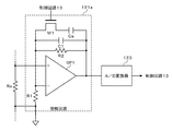
- FIG. 5 is a diagram illustrating a first configuration example of the current detection circuit 12 according to the embodiment.
- the current detection circuit 12 includes an amplifier circuit 121a and an A / D converter 123.
- the amplifier circuit 121a amplifies the voltage across the shunt resistor Rs with a predetermined gain and outputs the amplified voltage to the A / D converter 123.
- the A / D converter 123 converts the analog signal input from the amplifier circuit 121 a into a digital signal and outputs the digital signal to the control circuit 13.
- the amplifier circuit 121a includes a first operational amplifier OP1, a first input resistor R1, a first feedback resistor R2, a first feedback capacitor C1, an additional capacitor Ca, and a mode changeover switch M1. These elements constitute a low-pass filter.
- the low-pass filter shown in FIG. 5 is a primary low-pass filter.
- the non-inverting input terminal and the inverting input terminal of the first operational amplifier OP1 are respectively connected to both ends of the shunt resistor Rs. Specifically, the high potential side terminal of the shunt resistor Rs is connected to the non-inverting input terminal of the first operational amplifier OP1, and the low potential side terminal of the shunt resistor Rs is connected to the inverting input terminal of the first operational amplifier OP1.
- the first input resistor R1 is connected between the inverting input terminal of the first operational amplifier OP1 and the low potential side terminal of the shunt resistor Rs.
- a first feedback resistor R2 is connected between the inverting input terminal of the first operational amplifier OP1 and the output terminal of the first operational amplifier OP1.
- a first feedback capacitor C1 is connected in parallel with the first feedback resistor R2 between the inverting input terminal of the first operational amplifier OP1 and the output terminal of the first operational amplifier OP1.
- an additional capacitor Ca is connected in parallel with the first feedback resistor R2 and the first feedback capacitor C1 between the inverting input terminal of the first operational amplifier OP1 and the output terminal of the first operational amplifier OP1.
- a mode switch M1 is inserted between the inverting input terminal of the first operational amplifier OP1 and the additional capacitor Ca.
- a MOSFET, a photo relay, a photo coupler, or the like can be used for the mode switch M1.
- the mode switch M1 is turned on / off in response to a control signal from the control circuit 13.
- the gain Av of the amplifier circuit 121a is equal to the resistance value of the first input resistor R1 and the first feedback resistor R2, as shown in the following equation (1). It is set based on the ratio of resistance values. Further, since the configuration of the amplifier circuit 121a shown in FIG. 5 is a configuration of a non-inverting amplifier, the sign of the gain A is positive. When the inverting amplifier configuration is adopted, the sign of gain A is negative.
- the control circuit 13 can change the transfer characteristic of the amplifier circuit 121a by switching on / off of the mode switch M1.
- the control circuit 13 controls the mode switch M1 to be in an ON state, thereby lowering the high-frequency cutoff frequency of the amplifier circuit 121a. More specifically, the control circuit 13 lowers the high-frequency cutoff frequency of the amplifier circuit 121a while the secondary battery E1 is charged with the DC power generated by full-wave rectification of the AC power of the commercial power supply. That is, the control circuit 13 controls the mode switch M1 to be in an on state during the charging mode, and controls the mode switch M1 to be in an off state during other modes.
- the quick charge mode may be included or excluded from the charge mode.
- the current detection error can be suppressed to a low level without reducing the high-frequency cutoff frequency of the amplifier circuit 121a.
- the regenerative charging mode may be included or excluded from the charging mode. Since the ripple of the electric power generated by the traveling motor 40 based on the deceleration energy changes irregularly and the high frequency component is relatively small, the current detection error can be achieved without lowering the high frequency cutoff frequency of the amplifier circuit 121a. Can be kept small. On the other hand, since the ripple current during normal charging is large, it is necessary to lower the high-frequency cutoff frequency of the amplifier circuit 121a to attenuate more high-frequency components.
- Equation (2) represents the high-frequency cutoff frequency fc1 when the mode changeover switch M1 is in the off state
- Equation (3) represents the high-frequency cutoff frequency fc2 when the mode changeover switch M1 is in the on state.
- the low-pass filter has a configuration capable of selecting the first cutoff frequency fc and the second cutoff frequency f2 lower than the first cutoff frequency.
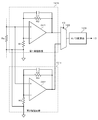
- FIG. 6 is a diagram illustrating a second configuration example of the current detection circuit 12 according to the embodiment.
- the current detection circuit 12 includes a first amplifier circuit 121b, a second amplifier circuit 121c, a multiplexer 122, and an A / D converter 123.
- two amplifier circuits having different transfer characteristics are provided.
- the first amplifier circuit 121b amplifies the voltage across the shunt resistor Rs with a predetermined gain and outputs the amplified voltage to the multiplexer 122.
- the second amplifier circuit 121c is connected in parallel with the first amplifier circuit 121b, amplifies the voltage across the shunt resistor Rs with a predetermined gain, and outputs the amplified voltage to the multiplexer 122.
- the multiplexer 122 selects the output of the first amplifier circuit 121 b and the output of the second amplifier circuit 121 c and outputs them to the A / D converter 123.
- the A / D converter 123 converts the analog signal input from the multiplexer 122 into a digital signal and outputs the digital signal to the control circuit 13.
- the first amplifier circuit 121b includes a first operational amplifier OP1, a first input resistor R1, a first feedback resistor R2, and a first feedback capacitor C1, and these elements constitute a low-pass filter.
- the non-inverting input terminal and the inverting input terminal of the first operational amplifier OP1 are respectively connected to both ends of the shunt resistor Rs.
- the high potential side terminal of the shunt resistor Rs is connected to the non-inverting input terminal of the first operational amplifier OP1
- the low potential side terminal of the shunt resistor Rs is connected to the inverting input terminal of the first operational amplifier OP1.
- the first input resistor R1 is connected between the inverting input terminal of the first operational amplifier OP1 and the low potential side terminal of the shunt resistor Rs.
- a first feedback resistor R2 is connected between the inverting input terminal of the first operational amplifier OP1 and the output terminal of the first operational amplifier OP1.
- a first feedback capacitor C1 is connected in parallel with the first feedback resistor R2 between the inverting input terminal of the first operational amplifier OP1 and the output terminal of the first operational amplifier OP1.
- the second amplifier circuit 121c includes a second operational amplifier OP2, a second input resistor R3, a second feedback resistor R4, and a second feedback capacitor C2, and these elements constitute a low-pass filter.
- the non-inverting input terminal and the inverting input terminal of the second operational amplifier OP2 are respectively connected to both ends of the shunt resistor Rs.
- the high potential side terminal of the shunt resistor Rs is connected to the non-inverting input terminal of the second operational amplifier OP2
- the low potential side terminal of the shunt resistor Rs is connected to the inverting input terminal of the second operational amplifier OP2.
- the second input resistor R3 is connected between the inverting input terminal of the second operational amplifier OP2 and the low potential side terminal of the shunt resistor Rs.
- a second feedback resistor R4 is connected between the inverting input terminal of the second operational amplifier OP2 and the output terminal of the second operational amplifier OP2.
- a second feedback capacitor C2 is connected in parallel with the second feedback resistor R4 between the inverting input terminal of the second operational amplifier OP2 and the output terminal of the second operational amplifier OP2.
- the first amplifier circuit 121b is designed to be equivalent to a circuit in which the mode switch M1 of the amplifier circuit 121a shown in FIG.
- the second amplifier circuit 121c is designed to be equivalent to a circuit in which the mode switch M1 of the amplifier circuit 121a shown in FIG.
- the capacitance value of the second feedback capacitor C2 is set larger than the capacitance value of the first feedback capacitor C1.
- Other circuit constants and operational amplifier specifications are set to be the same for the first amplifier circuit 121b and the second amplifier circuit 121c.
- the control circuit 13 can change the transfer characteristic of the amplifier circuit by inputting a switching signal to the multiplexer 122. Specifically, during charging of the secondary battery E1 from the AC power supply outside the vehicle, the control circuit 13 inputs a switching signal for selecting the output of the second amplifier circuit 121c to the multiplexer 122, whereby the amplifier circuit Lower the high frequency cutoff frequency. That is, the control circuit 13 inputs a switching signal for selecting the output of the second amplifier circuit 121c in the charging mode to the multiplexer 122, and outputs a switching signal for selecting the output of the first amplifier circuit 121b in the other modes. Input to the multiplexer 122. Whether or not to include the quick charge mode and / or the regenerative charge mode in the charge mode is as described above.
- the secondary battery E1 in the vehicle is charged from the commercial power source. Reduces ripple effects at low cost. That is, since the current detection sampling frequency is close to the commercial power supply ripple frequency, current detection errors may accumulate. In contrast, in the present embodiment, when charging from a commercial power source, the current detection error can be reduced by lowering the high-frequency cutoff frequency of the amplifier circuit and cutting more high-frequency components. When the commercial power source is not charged, high-precision current detection can be realized by setting the high-frequency cutoff frequency of the amplifier circuit in the vicinity of the Nyquist frequency of the sampling frequency.
- the multiplexer 122 is provided, and the output of the first amplifier circuit 121b and the output of the second amplifier circuit 121c are selected according to the mode.
- the multiplexer 122 is not provided, and two A / D converters for the first amplifier circuit 121b and the second amplifier circuit 121c are provided.
- the control circuit 13 selects the output digital value of the first amplifying circuit 121b and the output digital value of the second amplifying circuit 121c respectively input from the two AD converters according to the mode.
- the shunt resistor Rs is used as the current detection element.
- a Hall element may be used instead of the shunt resistor Rs.
- a passive filter composed only of passive elements can be used instead of an active filter having an amplification function using the above-described operational amplifier.
- the first cutoff frequency characteristic and the second cutoff frequency characteristic can be selected by varying the capacitance value of the capacitor.
Landscapes
- Engineering & Computer Science (AREA)
- Power Engineering (AREA)
- Transportation (AREA)
- Mechanical Engineering (AREA)
- Manufacturing & Machinery (AREA)
- Chemical & Material Sciences (AREA)
- Chemical Kinetics & Catalysis (AREA)
- Electrochemistry (AREA)
- General Chemical & Material Sciences (AREA)
- Electric Propulsion And Braking For Vehicles (AREA)
- Charge And Discharge Circuits For Batteries Or The Like (AREA)
- Measurement Of Current Or Voltage (AREA)
- Amplifiers (AREA)
Abstract
商用電源から車両内の二次電池に充電する場合にて、低コストでリプルの影響を抑制する。車両(100)内に搭載されるべき電源装置(10)において、二次電池(E1)は、走行用モータ(40)に電力を供給する。電流検出素子は、二次電池(E1)に流れる電流を検出する。電流検出回路(12)は、ローパスフィルタを介して、電流検出素子の信号電圧を取得し、取得した電圧値から二次電池(E1)に流れる電流の電流値を推定する。ローパスフィルタは、少なくとも第1の遮断周波数と、該第1の遮断周波数より低い第2の遮断周波数とを選択可能に構成されると共に、車両外の電源から二次電池(E1)が充電される際、第2の遮断周波数が選択される。
Description
本発明は、車両に搭載されるべき電源装置に関する。
近年、プラグインハイブリッド車(PHV)、電気自動車(EV)が普及してきている。PHV及びEVでは、車外から専用の充電ケーブルによって車内の電池に充電する必要がある。充電器には大別すると普通充電器と急速充電器がある。普通充電器は急速充電器より充電時間がかかるが、フル充電が可能であり設備導入コストを低く抑えられる。住宅、事務所、時間貸駐車場など長時間駐車する場所への設置が想定される。一方、急速充電器は短時間で80%充電が可能であるが、設備導入コストが高くなる。ショッピングセンター、ガソリンスタンド、高速道路SAなど滞在時間が短い場所への設置が想定される。
日本では普通充電器の電源に、家庭で一般に使用される単相交流200Vまたは100Vが使用されている。急速充電器の電源には、三相交流200Vが使用されている。普通充電器は単相電源を使用するため低コストではあるが電力リプルが大きく発生する。一方、急速充電器は三相交流を使用するため電力の輸送効率が高く電力リプルも小さいが、一般家庭で使用する場合は専用線を敷く必要がある。
商用電源から充電する場合、充電電流にリプルが発生する。特に単相交流を使用した場合、三相交流を使用した場合より、リプルが大きくなる。リプルの影響が大きくなると二次電池側で正確な電流を検出できなくなる。充電器の出力側に大規模な平滑フィルタを設ければ、リプルを低減できるがコスト増となる。
本発明はこうした状況に鑑みなされたものであり、その目的は、商用電源から車両内の二次電池に充電する場合にて、低コストでリプルの影響を抑制する技術を提供することにある。
上記課題を解決するために、本発明のある態様の電源装置は、車両内に搭載されるべき電源装置であって、走行用モータに電力を供給するための二次電池と、前記二次電池に流れる電流を検出するための電流検出素子と、所定の遮断周波数特性を有し、遮断周波数以下の信号を通過させるローパスフィルタと、前記ローパスフィルタを介して、前記電流検出素子の信号電圧を取得し、取得した電圧値から前記二次電池に流れる電流の電流値を推定する電流検出回路と、を備える。前記ローパスフィルタは、少なくとも第1の遮断周波数特性と、該第1の遮断周波数特性より低い第2の遮断周波数特性とを選択可能に構成されると共に、車両外の電源から前記二次電池が充電される際、第2の遮断周波数が選択される。
本発明によれば、商用電源から車両内の二次電池に充電する場合にて、低コストでリプルの影響を抑制できる。
図1は、本発明の実施の形態に係る電源装置10を搭載した車両100の構成を示す図である。本実施の形態では車両100として、商用電源(系統電源)から充電可能なプラグインハイブリッド車(PHV)又は電気自動車(EV)を想定する。
車両100は、電源装置10、車載充電器20、インバータ30及び走行用モータ40を備える。電源装置10は、二次電池E1、シャント抵抗Rs、電圧検出回路11、電流検出回路12、制御回路13を備える。二次電池E1は走行用モータ40に電力を供給するためのエネルギーを蓄えるための二次電池である。二次電池E1には例えば、ニッケル水素電池またはリチウムイオン電池を用いることができる。二次電池E1は、複数の電池セルが直列接続または直並列接続されて構成される。
二次電池E1は、車両100の外に設置された電源から充電される。上述のように充電設備には大別すると普通充電器と急速充電器がある。車両100内には、普通充電器から二次電池E1に充電するための普通充電経路と、急速充電器から二次電池E1に充電するための急速充電経路が別に設けられる。
普通充電経路上には車載充電器20、第1普通充電用スイッチS5、第2普通充電用スイッチS6が設けられる。車載充電器20は、充電ケーブルで接続された外部の普通充電器から入力される交流電力を直流電力に変換して二次電池E1に出力する。車載充電器20は、普通充電の開始および終了を制御回路13に通知する。
第1普通充電用スイッチS5は車載充電器20のプラス端子と、二次電池E1のプラス端子間の配線に挿入され、第2普通充電用スイッチS6は車載充電器20のマイナス端子と、二次電池E1のマイナス端子間の配線に挿入される。第1普通充電用スイッチS5及び第2普通充電用スイッチS6には、リレーを用いることができる。制御回路13は、普通充電時に第1普通充電用スイッチS5及び第2普通充電用スイッチS6をオン状態に制御し、それ以外のときオフ状態に制御する。
急速充電経路上には第1急速充電用スイッチS3及び第2急速充電用スイッチS4が設けられる。第1急速充電用スイッチS3は急速充電用差込口のプラス端子と、二次電池E1のプラス端子間の配線に挿入され、第2急速充電用スイッチS4は急速充電用差込口のマイナス端子と、二次電池E1のマイナス端子間の配線に挿入される。第1急速充電用スイッチS3及び第2急速充電用スイッチS4にも、リレーを用いることができる。制御回路13は、急速充電時に第1急速充電用スイッチS3及び第2急速充電用スイッチS4をオン状態に制御し、それ以外のときオフ状態に制御する。
図2は、車載充電器20の構成例を示すブロック図である。車載充電器20は、入力フィルタ21、全波整流回路22、PFC(Power Factor Correction)回路23、絶縁型DC-DCコンバータ24を備える。
入力フィルタ21は、普通充電器から供給される商用電源の交流電力から、商用電源周波数成分のみを帯域通過して全波整流回路22に出力する。全波整流回路22は、入力フィルタ21から入力される交流電力を全波整流してPFC回路23に出力する。全波整流回路22は例えば、4つの整流ダイオードがブリッジ構成で接続されたダイオードブリッジ回路で構成される。全波整流回路22により全波整流された直流電力には、リプルが含まれている。PFC回路23は、全波整流回路22から入力される直流電力の力率を改善して絶縁型DC-DCコンバータ24に出力する。
絶縁型DC-DCコンバータ24は、PFC回路23から入力される直流電圧を、設定された直流電圧に変換して二次電池E1に供給する。絶縁型DC-DCコンバータ24は、二次電池E1への出力電圧および出力電流を監視して、定電流充電(CC充電)または定電圧充電(CV充電)を実行する。絶縁型DC-DCコンバータ24には、フライバックDC-DCコンバータ、フォワードDC-DCコンバータ(プッシュプルDC-DCコンバータ、ハーフブリッジDC-DCコンバータ、フルブリッジDC-DCコンバータ)等を用いることができる。
図1に戻る。インバータ30は力行時、二次電池E1から供給される直流電力を交流電力に変換して走行用モータ40に供給する。回生時、走行用モータ40から供給される交流電力を直流電力に変換して二次電池E1に供給する。
走行用モータ40は自走可能な大型モータであってもよいし、エンジン走行(主に始動時および加速時の走行)をアシストする小型モータであってもよい。EV及びストロングタイプのPHVでは前者の大型モータが用いられ、小型のPHVでは後者の小型モータが用いられる。走行用モータ40は力行時、インバータ30から供給される直流電力に応じて回転する。回生時、減速による回転エネルギーを直流電力に変換してインバータ30に供給する。
二次電池E1のプラス端子と、インバータ30のプラス端子を繋ぐ経路の間に第1メインスイッチS1が挿入される。さらに第1メインスイッチS1と並列に、プリチャージスイッチSpとプリチャージ抵抗Rpの直列回路が接続される。二次電池E1のマイナス端子と、インバータ30のマイナス端子を繋ぐ経路の間に第2メインスイッチS2が挿入される。第1メインスイッチS1、第2メインスイッチS2、プリチャージスイッチSpには、リレーを用いることができる。
制御回路13は走行時、第1メインスイッチS1及び第2メインスイッチS2をオン状態に制御し、電源装置10と動力系を電気的に接続する。制御回路13は非走行時、原則として第1メインスイッチS1及び第2メインスイッチS2をオフ状態に制御し、電源装置10と動力系を電気的に遮断する。制御回路13は走行用モータ40の始動時、第1メインスイッチS1及び第2メインスイッチS2をターンオンする前に、プリチャージスイッチSpをターンオンする。これにより、インバータ30に並列接続された図示しないコンデンサにプリチャージでき、第1メインスイッチS1及び第2メインスイッチS2のターンオン時の突入電流を抑制できる。
電圧検出回路11は、二次電池E1を構成する各電池セルの電圧を検出する。電圧検出回路11は検出した各電池セルの電圧値を制御回路13に出力する。電圧検出回路11は、専用のカスタムICであるASIC(Application Specific Integrated Circuit)により構成される。
二次電池E1のマイナス端子にシャント抵抗Rsが直列に接続される。シャント抵抗Rsは、二次電池E1に流れる電流を検出するための電流検出素子である。なお電流検出素子として、シャント抵抗Rsの代わりにホール素子を用いてもよい。なおシャント抵抗Rsの挿入位置は、複数の電池セルが直列接続される経路上であれば、どの位置であってもよい。
電流検出回路12はシャント抵抗Rsの両端電圧をもとに、二次電池E1に流れる電流の値を検出する。電流検出回路12は検出した電流値を制御回路13に出力する。制御回路13はマイクロコンピュータで構成され、電源装置10全体を制御する。電流検出回路12及び制御回路13の詳細は後述する。
商用電源から充電する場合にて、充電器に十分なリプル除去能力がない場合、電力のリプルに合わせてリプル電流が発生する可能性がある。急速充電の場合、高仕様な急速充電器が用いられるため、十分なリプル除去能力を確保できる。具体的には絶縁型DC-DCコンバータの二次側に大きな平滑コンデンサを設置して、リプル除去能力を高めることができる。また日本では急速充電器の電源に三相交流が使用されているため、発生するリプルが小さくなる。
一方、普通充電器の電源には単相交流が使用されているため、リプルが大きくなる。また車載充電器20の絶縁型DC-DCコンバータ24の二次側に、大きな平滑コンデンサを設置することも考えられるが、コストアップになるとともに、回路規模も大きくなる。車載用途の充電器では、できるだけ低コストで小型の充電器が求められる。充電器のコストダウンを考慮すると、リプルをある程度、残したままで充電できることが望まれる。
図3は、普通充電器から単相交流100Vで充電される場合の、電圧(AC)、電流(AC)、電力、充電電流の推移を示す図である。充電電流(負荷電流)は固定値としている。商用電源の周波数は50/60Hzであり、以下の説明では50Hzを想定する。電圧(AC)と電流(AC)が同じ周波数であるため、発生する電力のリプルの周波数は商用周波数の2倍となる。電力を電池電圧で除した充電電流にも、商用周波数の2倍の周波数のリプル電流が発生する。
充電時に発生するリプル電流は、商用電源の周波数により決定されるため規則的に変化する。これに対して走行時に発生するリプル電流は、走行時の負荷に依存するため不規則に変化する傾向がある。従って商用電源から充電しないタイプのハイブリッド車(HV)ではリプル電流が、電圧検出や電流検出などに悪影響を与えることが少なかった。
電圧検出回路11及び電流検出回路12のサンプリング周期を含む電源装置10内の制御周期は、比較的低速に設定される。例えば10ms(=100Hz)に設定される。車載用途の二次電池の制御周期としては10msで十分であり、これより高い制御周期に設定してもオーバースペックになる。
50Hzの商用電源から二次電池E1に充電し、二次電池E1の電圧値および電流値を10ms(=100Hz)でサンプリングする場合、リプル周波数とサンプリング周波数が一致することになる。周波数が一致すると、リプル電流が電流検出に悪影響を与えることになる。
図4は、二次電池E1に流れる電流と、サンプリング周期を示す図である。図4では10ms周期で電流をサンプリングする例を描いており、平均値をサンプリングするケース(中段の矢印参照)、ワースト最大のみサンプルするケース(上段の矢印参照)、ワースト最小のみサンプルするケース(下段の矢印参照)を描いている。充電電流の平均値をサンプリングできれば、実際の電流値と検出した電流値に誤差が発生しないが、平均値以外でサンプリングするケースでは誤差が発生する。サンプリングポイントが平均値が離れるほど誤差が大きくなる。検出した電流値は積算しても使用される。例えば、二次電池E1のSOC(State Of Charge)は電流積算値にもとづき算出される。実際の電流値と検出した電流値の誤差が小さい場合でも積算値では大きな誤差となる場合がある。サンプリング周波数が100Hzの場合、ナイキスト周波数の50Hz以上の成分が偽信号となるため、大きな誤差になりやすい。
ナイキスト周波数以上の成分は、コンデンサ、コイル、抵抗などの受動素子のみで構成されたパッシブ型のアンチエイリアシングフィルタで除去することが一般的である。しかしながら、高域成分を十分に減衰させるアンチエイリアシングフィルタは、部品バラツキに起因する固体差が大きい。
バッテリ走行時は商用電源から充電する時のように、特定の周波数においての大きなリプル電流が発生することは少なく、これによる電流検出誤差は小さい。そのため、商用電源から充電しないタイプのHVでは、アンチエイリアシングフィルタの遮断周波数をナイキスト周波数より若干低域に設定することが一般的である。電流検出の必要帯域は制御周波数に依存し、例えば100Hz周期でサンプリングする場合、50Hz付近以上から減衰するようにフィルタを設計する。電圧検出と電流検出の同期をそろえるためである。
これに対して、商用電源から充電するタイプのPHV及びEVでは、商用電源からの充電時に大きなリプル電流が発生する。この場合にて、ナイキスト周波数より若干低い程度の遮断周波数のフィルタを使用すると、正確な電流値および電流積算値が得られなくなる可能性が高い。
この問題はサンプリング周波数をリプル周波数より十分に高く(例えば、4倍以上)設定すれば解決できるが、より高速なマイクロコンピュータが必要となる。高速なマイクロコンピュータはコストアップにつながり、消費電力も大きくなる。
ここまでリプル電流による電流検出誤差について説明した。電圧検出誤差については、電池の内部抵抗が小さいため、大きなリプル電流が発生してもリプル電圧の上昇は限定的である。そのため電圧検出誤差は、電流検出誤差ほど大きな問題にならない。以下、大きなパッシブ型のフィルタを用いずに電流検出誤差を低減する手法を説明する。
図5は、実施の形態に係る電流検出回路12の第1構成例を示す図である。第1構成例では電流検出回路12は、増幅回路121a及びA/D変換器123を備える。増幅回路121aは、シャント抵抗Rsの両端電圧を所定のゲインで増幅してA/D変換器123に出力する。A/D変換器123は、増幅回路121aから入力されるアナログ信号をデジタル信号に変換して制御回路13に出力する。
増幅回路121aは、第1オペアンプOP1、第1入力抵抗R1、第1帰還抵抗R2、第1帰還容量C1、追加容量Ca、モード切替スイッチM1を含む。これらの素子でローパスフィルタを構成している。図5に示す当該ローパスフィルタは1次ローパスフィルタである。
第1オペアンプOP1の非反転入力端子および反転入力端子は、シャント抵抗Rsの両端にそれぞれ接続される。具体的には第1オペアンプOP1の非反転入力端子にシャント抵抗Rsの高電位側端子が接続され、第1オペアンプOP1の反転入力端子にシャント抵抗Rsの低電位側端子が接続される。
第1オペアンプOP1の反転入力端子とシャント抵抗Rsの低電位側端子の間に第1入力抵抗R1が接続される。第1オペアンプOP1の反転入力端子と第1オペアンプOP1の出力端子間に第1帰還抵抗R2が接続される。第1オペアンプOP1の反転入力端子と第1オペアンプOP1の出力端子間に、第1帰還抵抗R2と並列に第1帰還容量C1が接続される。さらに第1オペアンプOP1の反転入力端子と第1オペアンプOP1の出力端子間に、第1帰還抵抗R2及び第1帰還容量C1と並列に追加容量Caが接続される。第1オペアンプOP1の反転入力端子と追加容量Ca間にモード切替スイッチM1が挿入される。
モード切替スイッチM1にはMOSFET、フォトリレー、フォトカプラ等を用いることができる。モード切替スイッチM1は、制御回路13からの制御信号に応じてオン/オフする。なお増幅回路121aと制御回路13を絶縁するために、モード切替スイッチM1にはフォトリレー又はフォトカプラを使用することが望ましい。
第1オペアンプOP1の反転入力端子が仮想接地しているとみなせるため、増幅回路121aのゲインAvは下記式(1)に示すように、第1入力抵抗R1の抵抗値と第1帰還抵抗R2の抵抗値の比にもとづき設定される。また図5に示す増幅回路121aの構成は、非反転増幅器の構成であるため、ゲインAの符号は正である。なお反転増幅器の構成を採用した場合、ゲインAの符号は負になる。
Av=(R2/R1)+1 ・・・式(1)
制御回路13は、モード切替スイッチM1のオン/オフを切り替えることにより、増幅回路121aの伝達特性を変えることができる。車両外の交流電源から二次電池E1への充電中、制御回路13はモード切替スイッチM1をオン状態に制御することにより、増幅回路121aの高域遮断周波数を下げる。より具体的には、商用電源の交流電力が全波整流されて生成された直流電力が二次電池E1に充電されている間、制御回路13は増幅回路121aの高域遮断周波数を下げる。即ち制御回路13は、充電モード時にモード切替スイッチM1をオン状態に制御し、それ以外のモード時にモード切替スイッチM1をオフ状態に制御する。
制御回路13は、モード切替スイッチM1のオン/オフを切り替えることにより、増幅回路121aの伝達特性を変えることができる。車両外の交流電源から二次電池E1への充電中、制御回路13はモード切替スイッチM1をオン状態に制御することにより、増幅回路121aの高域遮断周波数を下げる。より具体的には、商用電源の交流電力が全波整流されて生成された直流電力が二次電池E1に充電されている間、制御回路13は増幅回路121aの高域遮断周波数を下げる。即ち制御回路13は、充電モード時にモード切替スイッチM1をオン状態に制御し、それ以外のモード時にモード切替スイッチM1をオフ状態に制御する。
充電モードに、急速充電モードを含めてもよいし除外してもよい。上述のように三相交流を使用した急速充電時のリプル電流は比較的小さいため、増幅回路121aの高域遮断周波数を下げなくても、電流検出誤差を小さく抑えることができる。また充電モードに、回生充電モードを含めてもよいし除外してもよい。減速エネルギーをもとに走行用モータ40により発電された電力のリプルは不規則に変化し、高域成分も比較的少ないため、増幅回路121aの高域遮断周波数を下げなくても、電流検出誤差を小さく抑えることができる。これに対して普通充電時のリプル電流が大きいため、増幅回路121aの高域遮断周波数を下げて、より多くの高域成分を減衰させる必要がある。
1次ローパスフィルタとして機能する増幅回路121aの第1の高域遮断周波数fc1、第2の高域遮断周波数fc2は、下記式(2)、式(3)により表される。式(2)がモード切替スイッチM1がオフ状態の高域遮断周波数fc1を示し、式(3)がモード切替スイッチM1がオン状態の高域遮断周波数fc2を示す。このように当該ローパスフィルタは、第1の遮断周波数fcと、当該第1の遮断周波数より低い第2の遮断周波数f2を選択可能な構成である。
fc1=1/(2π・R2/C1) ・・・式(2)
fc1=1/(2π・R2/(C1+Ca) ・・・式(3)
仮にゲインAv=50、走行時の高域遮断周波数fc1=48Hz、充電時の高域遮断周波数fc2=10Hzと設定する場合、例えば回路定数をR1=1kΩ、R2=49kΩ、C1=67nF、Ca=257nFに設定すればよい。
fc1=1/(2π・R2/(C1+Ca) ・・・式(3)
仮にゲインAv=50、走行時の高域遮断周波数fc1=48Hz、充電時の高域遮断周波数fc2=10Hzと設定する場合、例えば回路定数をR1=1kΩ、R2=49kΩ、C1=67nF、Ca=257nFに設定すればよい。
図6は、実施の形態に係る電流検出回路12の第2構成例を示す図である。第2構成例では電流検出回路12は、第1増幅回路121b、第2増幅回路121c、マルチプレクサ122及びA/D変換器123を備える。構成例2では、伝達特性の異なる2つの増幅回路を設ける。
第1増幅回路121bは、シャント抵抗Rsの両端電圧を所定のゲインで増幅してマルチプレクサ122に出力する。第2増幅回路121cは第1増幅回路121bと並列接続され、シャント抵抗Rsの両端電圧を所定のゲインで増幅してマルチプレクサ122に出力する。マルチプレクサ122は、第1増幅回路121bの出力と第2増幅回路121cの出力を選択してA/D変換器123に出力する。A/D変換器123は、マルチプレクサ122から入力されるアナログ信号をデジタル信号に変換して制御回路13に出力する。
第1増幅回路121bは、第1オペアンプOP1、第1入力抵抗R1、第1帰還抵抗R2、第1帰還容量C1を含み、これらの素子でローパスフィルタを構成している。第1オペアンプOP1の非反転入力端子および反転入力端子は、シャント抵抗Rsの両端にそれぞれ接続される。具体的には第1オペアンプOP1の非反転入力端子にシャント抵抗Rsの高電位側端子が接続され、第1オペアンプOP1の反転入力端子にシャント抵抗Rsの低電位側端子が接続される。
第1オペアンプOP1の反転入力端子とシャント抵抗Rsの低電位側端子の間に第1入力抵抗R1が接続される。第1オペアンプOP1の反転入力端子と第1オペアンプOP1の出力端子間に第1帰還抵抗R2が接続される。さらに第1オペアンプOP1の反転入力端子と第1オペアンプOP1の出力端子間に、第1帰還抵抗R2と並列に第1帰還容量C1が接続される。
第2増幅回路121cは、第2オペアンプOP2、第2入力抵抗R3、第2帰還抵抗R4、第2帰還容量C2を含み、これらの素子でローパスフィルタを構成している。第2オペアンプOP2の非反転入力端子および反転入力端子は、シャント抵抗Rsの両端にそれぞれ接続される。具体的には第2オペアンプOP2の非反転入力端子にシャント抵抗Rsの高電位側端子が接続され、第2オペアンプOP2の反転入力端子にシャント抵抗Rsの低電位側端子が接続される。
第2オペアンプOP2の反転入力端子とシャント抵抗Rsの低電位側端子の間に第2入力抵抗R3が接続される。第2オペアンプOP2の反転入力端子と第2オペアンプOP2の出力端子間に第2帰還抵抗R4が接続される。さらに第2オペアンプOP2の反転入力端子と第2オペアンプOP2の出力端子間に、第2帰還抵抗R4と並列に第2帰還容量C2が接続される。
第1増幅回路121bは、図5に示した増幅回路121aのモード切替スイッチM1がオフ状態の回路と等価に設計する。第2増幅回路121cは、図5に示した増幅回路121aのモード切替スイッチM1がオフ状態の回路と等価に設計する。そのために、第2帰還容量C2の容量値を、第1帰還容量C1の容量値より大きく設定する。それ以外の回路定数およびオペアンプの仕様は、第1増幅回路121bと第2増幅回路121cで同じに設定する。
制御回路13は、マルチプレクサ122に切替信号を入力して、増幅回路の伝達特性を変えることができる。具体的には車両外の交流電源から二次電池E1への充電中、制御回路13は、第2増幅回路121cの出力を選択するための切替信号をマルチプレクサ122に入力することにより、増幅回路の高域遮断周波数を下げる。即ち制御回路13は、充電モード時に第2増幅回路121cの出力を選択するための切替信号をマルチプレクサ122に入力し、それ以外のモード時に第1増幅回路121bの出力を選択するための切替信号をマルチプレクサ122に入力する。充電モードに、急速充電モード及び/又は回生充電モードを含めるか否かは上述の通りである。
以上説明したように本実施の形態によれば、電流検出回路12内の増幅回路の伝達特性を、モードに応じて切り替えることにより、商用電源から車両内の二次電池E1に充電する場合にて、低コストでリプルの影響を抑制する。即ち、電流検出のサンプリング周波数と商用電源のリプル周波数が近いため、電流検出誤差が累積してしまう可能性がある。これに対して本実施の形態では商用電源からの充電時に、増幅回路の高域遮断周波数を下げて、より多くの高域成分をカットすることにより、電流検出誤差を低減できる。また商用電源から充電していないときは、増幅回路の高域遮断周波数を、サンプリング周波数のナイキスト周波数近辺に設定することにより、高精度な電流検出を実現できる。
また充電時に電流検出回路12内の増幅回路で、大きなローパスフィルタをかけることにより、充電器の平滑フィルタを大規模化する必要がなくなる。従って充電器のコストアップを抑えることができる。
電流検出回路12内の増幅回路を、図5のように構成すると部品点数の増加を最小限に抑えることができ回路面積の増加も最小限に抑えることができる。なお、モード切替スイッチM1に使用するフォトリレー等の価格によっては、図6に示したように同じ回路構成でフィルタ特性が異なる増幅回路を2つ設けたほうが安価に構成できる場合もある。
以上、本発明を実施の形態をもとに説明した。こられ実施の形態は例示であり、それらの各構成要素や各処理プロセスの組合せにいろいろな変形例が可能なこと、またそうした変形例も本発明の範囲にあることは当業者に理解されるところである。
例えば図6に示した構成例2ではマルチプレクサ122を設けて、モードに応じて第1増幅回路121bの出力と第2増幅回路121cの出力を選択した。構成例2の変形例では、マルチプレクサ122を設けずに、第1増幅回路121b用と第2増幅回路121c用の2つのA/D変換器をそれぞれ設ける。制御回路13は、2つのAD変換器からそれぞれ入力される第1増幅回路121bの出力デジタル値と、第2増幅回路121cの出力デジタル値を、モードに応じて選択する。
上記の実施の形態では電流検出素子としてシャント抵抗Rsを用いる例を示したが、シャント抵抗Rsの代わりにホール素子を用いてもよい。その場合、ホール素子から直接、電流値に相当する電圧値が得られるため、上述のオペアンプを用いた増幅機能を有するアクティブフィルタでなく、パッシブ素子だけで構成されたパッシブフィルタを用いることができる。その場合も同様に、コンデンサの容量値を可変させることにより、第1の遮断周波数特性と、第2の遮断周波数特性を選択できる。
100 車両、 E1 二次電池、 Rs シャント抵抗、 S1 第1メインスイッチ、 S2 第2メインスイッチ、 Sp プリチャージスイッチ、 Rp プリチャージ抵抗、 S3 第1急速充電用スイッチ、 S4 第2急速充電用スイッチ、 S5 第1普通充電用スイッチ、 S6 第2普通充電用スイッチ、 10 電源装置、 11 電圧検出回路、 12 電流検出回路、 121a 増幅回路、 OP1 第1オペアンプ、 R1 第1入力抵抗、 R2 第1帰還抵抗、 C1 第1帰還容量、 Ca 追加容量、 M1 モード切替スイッチ、 OP2 第2オペアンプ、 R3 第2入力抵抗、 R4 第2帰還抵抗、 C2 第2帰還容量、 121b 第1増幅回路、 121c 第2増幅回路、 122 マルチプレクサ、 123 A/D変換器、 13 制御回路、 20 車載充電器、 21 入力フィルタ、 22 全波整流回路、 23 PFC回路、 24 絶縁型DC-DCコンバータ、 30 インバータ、 40 走行用モータ。
Claims (4)
- 車両内に搭載されるべき電源装置であって、
走行用モータに電力を供給するための二次電池と、
前記二次電池に流れる電流を検出するための電流検出素子と、
所定の遮断周波数特性を有し、遮断周波数以下の信号を通過させるローパスフィルタと、
前記ローパスフィルタを介して、前記電流検出素子の信号電圧を取得し、取得した電圧値から前記二次電池に流れる電流の電流値を推定する電流検出回路と、を備え、
前記ローパスフィルタは、少なくとも第1の遮断周波数特性と、該第1の遮断周波数特性より低い第2の遮断周波数特性とを選択可能に構成されると共に、車両外の電源から前記二次電池が充電される際、第2の遮断周波数が選択されることを特徴とする電源装置。 - 前記ローパスフィルタは、
前記電流検出素子の両端に接続されるオペアンプと、
前記電流検出素子の一端と前記オペアンプの一方の入力端子間に接続される入力抵抗と、
前記オペアンプの一方の入力端子と前記オペアンプの出力端子間に接続される帰還抵抗と、
前記オペアンプの一方の入力端子と前記オペアンプの出力端子間に前記帰還抵抗と並列に接続される第1帰還容量と、
前記オペアンプの一方の入力端子と前記オペアンプの出力端子間に前記帰還抵抗および前記第1帰還容量と並列接続される追加容量と、
前記オペアンプの一方の入力端子と前記追加容量の間に挿入されるスイッチと、を含み、
前記スイッチは、充電モード時にオンし、非充電モード時にオフすることを特徴とする請求項1に記載の電源装置。 - 前記ローパスフィルタは第1増幅回路および第2増幅回路を含み、
前記第1増幅回路は、
前記電流検出素子の両端に接続される第1オペアンプと、
前記電流検出素子の一端と前記第1オペアンプの一方の入力端子間に接続される第1入力抵抗と、
前記第1オペアンプの一方の入力端子と前記第1オペアンプの出力端子間に接続される第1帰還抵抗と、
前記第1オペアンプの一方の入力端子と前記第1オペアンプの出力端子間に前記第1帰還抵抗と並列接続される第1帰還容量と、を含み、
前記第2増幅回路は、
前記電流検出素子の両端に接続される第2オペアンプと、
前記電流検出素子の一端と前記第2オペアンプの一方の入力端子間に接続される第2入力抵抗と、
前記第2オペアンプの一方の入力端子と前記第2オペアンプの出力端子間に接続される第2帰還抵抗と、
前記第2オペアンプの一方の入力端子と前記第2オペアンプの出力端子間に前記第2帰還抵抗と並列接続される第2帰還容量と、を含み、
前記第2帰還容量の容量値が、前記第1帰還容量の容量値より大きく設定され、
前記電流検出回路は、
前記第1増幅回路の出力と前記第2増幅回路の出力を選択する選択回路をさらに備え、
前記選択回路は、充電モード時に前記第2増幅回路の出力を選択し、非充電モード時に前記第1増幅回路の出力を選択することを特徴とする請求項1に記載の電源装置。 - 前記ローパスフィルタは、商用電源の交流電力が全波整流されて生成された直流電力が、前記二次電池に充電されている間、前記第2の遮断周波数以下の信号を通過させることを特徴とする請求項1から3のいずれかに記載の電源装置。
Priority Applications (1)
| Application Number | Priority Date | Filing Date | Title |
|---|---|---|---|
| JP2015552298A JP6456843B2 (ja) | 2013-12-11 | 2014-11-18 | 電源装置 |
Applications Claiming Priority (2)
| Application Number | Priority Date | Filing Date | Title |
|---|---|---|---|
| JP2013-256241 | 2013-12-11 | ||
| JP2013256241 | 2013-12-11 |
Publications (1)
| Publication Number | Publication Date |
|---|---|
| WO2015087488A1 true WO2015087488A1 (ja) | 2015-06-18 |
Family
ID=53370822
Family Applications (1)
| Application Number | Title | Priority Date | Filing Date |
|---|---|---|---|
| PCT/JP2014/005767 Ceased WO2015087488A1 (ja) | 2013-12-11 | 2014-11-18 | 電源装置 |
Country Status (2)
| Country | Link |
|---|---|
| JP (1) | JP6456843B2 (ja) |
| WO (1) | WO2015087488A1 (ja) |
Cited By (11)
| Publication number | Priority date | Publication date | Assignee | Title |
|---|---|---|---|---|
| JP2019161382A (ja) * | 2018-03-12 | 2019-09-19 | ローム株式会社 | 増幅回路並びに増幅回路に関わる半導体装置及びドライバ装置 |
| EP3550696A1 (de) * | 2018-04-03 | 2019-10-09 | Volkswagen Aktiengesellschaft | Batteriesystem für ein kraftfahrzeug und kraftfahrzeug |
| CN110323795A (zh) * | 2018-03-30 | 2019-10-11 | 铃木株式会社 | 车辆用电源装置 |
| CN110323798A (zh) * | 2018-03-30 | 2019-10-11 | 铃木株式会社 | 车辆用电源装置 |
| CN110323797A (zh) * | 2018-03-30 | 2019-10-11 | 铃木株式会社 | 车辆用电源装置 |
| JP2019180157A (ja) * | 2018-03-30 | 2019-10-17 | スズキ株式会社 | 車両用電源装置 |
| JP2020088873A (ja) * | 2018-11-14 | 2020-06-04 | トヨタ自動車株式会社 | 車両 |
| JP2022092535A (ja) * | 2020-12-10 | 2022-06-22 | トヨタホーム株式会社 | 電力供給システム |
| JP2024526530A (ja) * | 2021-09-03 | 2024-07-19 | ビーワイディー カンパニー リミテッド | 配電器、車両の充電配電システム、車両及び充電スタンド |
| JP2024537044A (ja) * | 2021-09-28 | 2024-10-10 | イオントラ インコーポレイテッド | 車載ev充電器及び回生制動のためのシステム及び方法 |
| WO2025047491A1 (ja) * | 2023-08-31 | 2025-03-06 | ミツミ電機株式会社 | 電流検出アンプおよび電流検出用半導体装置 |
Families Citing this family (1)
| Publication number | Priority date | Publication date | Assignee | Title |
|---|---|---|---|---|
| JP7020247B2 (ja) * | 2018-03-30 | 2022-02-16 | スズキ株式会社 | 車両用電源装置 |
Citations (3)
| Publication number | Priority date | Publication date | Assignee | Title |
|---|---|---|---|---|
| JPH11332111A (ja) * | 1998-05-15 | 1999-11-30 | Seiko Instruments Inc | バッテリー状態監視回路及びバッテリー装置 |
| JP2010223781A (ja) * | 2009-03-24 | 2010-10-07 | Toshiba Corp | 電流積算回路装置およびこれを用いた二次電池パック |
| JP2013090473A (ja) * | 2011-10-19 | 2013-05-13 | Toyota Motor Corp | 蓄電システム及び電流センサ異常を検出する方法 |
-
2014
- 2014-11-18 WO PCT/JP2014/005767 patent/WO2015087488A1/ja not_active Ceased
- 2014-11-18 JP JP2015552298A patent/JP6456843B2/ja active Active
Patent Citations (3)
| Publication number | Priority date | Publication date | Assignee | Title |
|---|---|---|---|---|
| JPH11332111A (ja) * | 1998-05-15 | 1999-11-30 | Seiko Instruments Inc | バッテリー状態監視回路及びバッテリー装置 |
| JP2010223781A (ja) * | 2009-03-24 | 2010-10-07 | Toshiba Corp | 電流積算回路装置およびこれを用いた二次電池パック |
| JP2013090473A (ja) * | 2011-10-19 | 2013-05-13 | Toyota Motor Corp | 蓄電システム及び電流センサ異常を検出する方法 |
Cited By (21)
| Publication number | Priority date | Publication date | Assignee | Title |
|---|---|---|---|---|
| JP2019161382A (ja) * | 2018-03-12 | 2019-09-19 | ローム株式会社 | 増幅回路並びに増幅回路に関わる半導体装置及びドライバ装置 |
| JP7131028B2 (ja) | 2018-03-30 | 2022-09-06 | スズキ株式会社 | 車両用電源装置 |
| CN110323798B (zh) * | 2018-03-30 | 2023-07-04 | 铃木株式会社 | 车辆用电源装置 |
| CN110323795A (zh) * | 2018-03-30 | 2019-10-11 | 铃木株式会社 | 车辆用电源装置 |
| CN110323798A (zh) * | 2018-03-30 | 2019-10-11 | 铃木株式会社 | 车辆用电源装置 |
| CN110323797A (zh) * | 2018-03-30 | 2019-10-11 | 铃木株式会社 | 车辆用电源装置 |
| JP2019180153A (ja) * | 2018-03-30 | 2019-10-17 | スズキ株式会社 | 車両用電源装置 |
| JP2019180157A (ja) * | 2018-03-30 | 2019-10-17 | スズキ株式会社 | 車両用電源装置 |
| JP7214975B2 (ja) | 2018-03-30 | 2023-01-31 | スズキ株式会社 | 車両用電源装置 |
| KR20190116086A (ko) * | 2018-04-03 | 2019-10-14 | 폭스바겐 악티엔 게젤샤프트 | 자동차용 배터리 시스템 및 자동차 |
| KR102234119B1 (ko) | 2018-04-03 | 2021-04-02 | 폭스바겐 악티엔게젤샤프트 | 자동차용 배터리 시스템 및 자동차 |
| CN110350257B (zh) * | 2018-04-03 | 2022-07-26 | 大众汽车有限公司 | 用于机动车的电池系统和机动车 |
| CN110350257A (zh) * | 2018-04-03 | 2019-10-18 | 大众汽车有限公司 | 用于机动车的电池系统和机动车 |
| EP3550696A1 (de) * | 2018-04-03 | 2019-10-09 | Volkswagen Aktiengesellschaft | Batteriesystem für ein kraftfahrzeug und kraftfahrzeug |
| JP7010198B2 (ja) | 2018-11-14 | 2022-01-26 | トヨタ自動車株式会社 | 車両 |
| JP2020088873A (ja) * | 2018-11-14 | 2020-06-04 | トヨタ自動車株式会社 | 車両 |
| JP2022092535A (ja) * | 2020-12-10 | 2022-06-22 | トヨタホーム株式会社 | 電力供給システム |
| JP2024526530A (ja) * | 2021-09-03 | 2024-07-19 | ビーワイディー カンパニー リミテッド | 配電器、車両の充電配電システム、車両及び充電スタンド |
| JP2024537044A (ja) * | 2021-09-28 | 2024-10-10 | イオントラ インコーポレイテッド | 車載ev充電器及び回生制動のためのシステム及び方法 |
| EP4409716A4 (en) * | 2021-09-28 | 2025-08-13 | Iontra Inc | SYSTEMS AND METHODS FOR ELECTRIC VEHICLE (EV) ON-BOARD CHARGER AND REGENERATIVE BRAKING |
| WO2025047491A1 (ja) * | 2023-08-31 | 2025-03-06 | ミツミ電機株式会社 | 電流検出アンプおよび電流検出用半導体装置 |
Also Published As
| Publication number | Publication date |
|---|---|
| JPWO2015087488A1 (ja) | 2017-03-16 |
| JP6456843B2 (ja) | 2019-01-23 |
Similar Documents
| Publication | Publication Date | Title |
|---|---|---|
| JP6456843B2 (ja) | 電源装置 | |
| US8368347B2 (en) | Vehicular charging system | |
| KR101263463B1 (ko) | 배터리 충전 장치 | |
| JP6361493B2 (ja) | 車載バッテリの充電装置 | |
| US9676287B2 (en) | Electric battery charging installation and method | |
| US20170282747A1 (en) | Charging system for vehicle battery | |
| CN105914848B (zh) | 包括蓄电池充电系统的车辆 | |
| EP3675339A1 (en) | 3-phase dual active bridge dc/dc converter with auxilary secondary output | |
| JP5808678B2 (ja) | 電動車両 | |
| JP5817096B2 (ja) | 電力供給装置及び電力供給方法 | |
| WO2018073961A1 (ja) | 電源システム及びその制御方法 | |
| CN103091532A (zh) | 用于汽车的基于零磁通补偿的电流传感器 | |
| KR20150053452A (ko) | 전기자동차용 모듈식 차량 탑재형 완속 충전 시스템 및 충전 방법 | |
| KR20190076167A (ko) | 스마트 전기 자동차 충전 시스템 | |
| JP2010172093A (ja) | 車載用充電器 | |
| JP5661075B2 (ja) | 充放電装置 | |
| JP2012085447A (ja) | Ac−dcコンバータ | |
| KR101398224B1 (ko) | 전기 자동차용 저전압 직류 컨버터의 전류 검출 장치 | |
| US20140084694A1 (en) | Power management system comprising a power source, a source of renewable energy, and a power converter | |
| JP2011205806A (ja) | 車両用マルチフェーズコンバータ | |
| CN104205560A (zh) | 用于借助电网为至少一个电能存储单元充电的电路 | |
| JP5673504B2 (ja) | 車両の充電装置 | |
| WO2012073350A1 (ja) | 車両の電源システム | |
| Nguyen et al. | Battery charger with small DC-link capacitors for G2V applications | |
| Kurfirt et al. | E-mobility impact on supply in distribution grid |
Legal Events
| Date | Code | Title | Description |
|---|---|---|---|
| 121 | Ep: the epo has been informed by wipo that ep was designated in this application |
Ref document number: 14869313 Country of ref document: EP Kind code of ref document: A1 |
|
| ENP | Entry into the national phase |
Ref document number: 2015552298 Country of ref document: JP Kind code of ref document: A |
|
| NENP | Non-entry into the national phase |
Ref country code: DE |
|
| 122 | Ep: pct application non-entry in european phase |
Ref document number: 14869313 Country of ref document: EP Kind code of ref document: A1 |