WO2015068264A1 - 半導体装置 - Google Patents
半導体装置 Download PDFInfo
- Publication number
- WO2015068264A1 WO2015068264A1 PCT/JP2013/080258 JP2013080258W WO2015068264A1 WO 2015068264 A1 WO2015068264 A1 WO 2015068264A1 JP 2013080258 W JP2013080258 W JP 2013080258W WO 2015068264 A1 WO2015068264 A1 WO 2015068264A1
- Authority
- WO
- WIPO (PCT)
- Prior art keywords
- semiconductor device
- film
- titanium
- nitrogen
- nitride film
- Prior art date
- Legal status (The legal status is an assumption and is not a legal conclusion. Google has not performed a legal analysis and makes no representation as to the accuracy of the status listed.)
- Ceased
Links
Images


Classifications
-
- H—ELECTRICITY
- H10—SEMICONDUCTOR DEVICES; ELECTRIC SOLID-STATE DEVICES NOT OTHERWISE PROVIDED FOR
- H10D—INORGANIC ELECTRIC SEMICONDUCTOR DEVICES
- H10D64/00—Electrodes of devices having potential barriers
- H10D64/60—Electrodes characterised by their materials
- H10D64/66—Electrodes having a conductor capacitively coupled to a semiconductor by an insulator, e.g. MIS electrodes
- H10D64/667—Electrodes having a conductor capacitively coupled to a semiconductor by an insulator, e.g. MIS electrodes the conductor comprising a layer of alloy material, compound material or organic material contacting the insulator, e.g. TiN workfunction layers
-
- H—ELECTRICITY
- H10—SEMICONDUCTOR DEVICES; ELECTRIC SOLID-STATE DEVICES NOT OTHERWISE PROVIDED FOR
- H10D—INORGANIC ELECTRIC SEMICONDUCTOR DEVICES
- H10D64/00—Electrodes of devices having potential barriers
- H10D64/01—Manufacture or treatment
- H10D64/013—Manufacture or treatment of electrodes having a conductor capacitively coupled to a semiconductor by an insulator
- H10D64/01302—Manufacture or treatment of electrodes having a conductor capacitively coupled to a semiconductor by an insulator the insulator being formed after the semiconductor body, the semiconductor being silicon
- H10D64/01304—Manufacture or treatment of electrodes having a conductor capacitively coupled to a semiconductor by an insulator the insulator being formed after the semiconductor body, the semiconductor being silicon characterised by the conductor
- H10D64/01318—Manufacture or treatment of electrodes having a conductor capacitively coupled to a semiconductor by an insulator the insulator being formed after the semiconductor body, the semiconductor being silicon characterised by the conductor the conductor comprising a layer of alloy material, compound material or organic material contacting the insulator, e.g. TiN
-
- H—ELECTRICITY
- H10—SEMICONDUCTOR DEVICES; ELECTRIC SOLID-STATE DEVICES NOT OTHERWISE PROVIDED FOR
- H10D—INORGANIC ELECTRIC SEMICONDUCTOR DEVICES
- H10D64/00—Electrodes of devices having potential barriers
- H10D64/01—Manufacture or treatment
- H10D64/013—Manufacture or treatment of electrodes having a conductor capacitively coupled to a semiconductor by an insulator
- H10D64/01302—Manufacture or treatment of electrodes having a conductor capacitively coupled to a semiconductor by an insulator the insulator being formed after the semiconductor body, the semiconductor being silicon
- H10D64/01332—Making the insulator
- H10D64/01336—Making the insulator on single crystalline silicon, e.g. chemical oxidation using a liquid
- H10D64/01338—Making the insulator on single crystalline silicon, e.g. chemical oxidation using a liquid with a treatment, e.g. annealing, after the formation of the conductor
Definitions
- the present invention relates to a semiconductor device.
- CMOS device development using a metal gate electrode has been carried out.
- the threshold voltage of the transistor is determined by the impurity concentration of the channel region and the work function of the gate electrode.
- the work function of the gate electrode material is about 4.6 eV, which is a silicon midgap, in order to make the threshold voltages of the nMOS and pMOS equal to each other. It is desirable that
- a titanium metal target is used to adjust a mixing ratio of an argon gas flow rate and a nitrogen gas flow rate, and is formed on a titanium nitride film formed using a sputtering method such as PVD (Physical Vapor Deposition).
- a sputtering method such as PVD (Physical Vapor Deposition).
- An object of the present invention is to provide a semiconductor device having a desired effective work function by atomic layer deposition using an organic gas.
- a semiconductor device includes a gate oxide film formed on a silicon substrate and a gate electrode formed on the gate oxide film, and the gate electrode includes a titanium nitride film containing carbon.
- the polycrystalline silicon film, the silicon substrate, the gate oxide film, the titanium nitride film containing carbon, and the polycrystalline silicon film are 350 ° C. in an atmosphere containing hydrogen. It has been heat-treated as described above.
- the titanium nitride film is formed using tetrakis (ethylmethylamino) titanium and ammonia.
- the ratio of nitrogen to titanium of the titanium nitride film is 0.8 to 1.2.
- the thickness of the titanium nitride film is 4 nm to 8 nm.
- the silicon substrate, the gate oxide film, and the carbon-containing titanium nitride film are heat-treated in a nitrogen atmosphere at 900 ° C. or higher. It is characterized by.
- the gate oxide film is formed using an atmosphere containing oxygen at 800 ° C. or higher.
- a tantalum nitride film is formed on the polycrystalline silicon film.
- the polycrystalline silicon film is formed by a low pressure chemical vapor deposition apparatus.
- a semiconductor device having a desired effective work function can be provided by using atomic layer deposition using an organic gas.
- 1 is a cross-sectional view of a semiconductor device according to the present invention. It is the figure which showed the voltage dependence of the capacity
- FIG. 1 is a cross-sectional view of a semiconductor device according to the present invention.
- the gate oxide film 102 having a thickness of 5 nm was formed by oxidizing the 6 ⁇ 10 15 cm ⁇ 3 p-type silicon substrate 101 using an atmosphere of oxygen diluted with nitrogen at 1000 ° C.
- titanium nitride films 103 were deposited on the gate oxide film 102 by ALD (Atomic Layer Deposition) using tetrakis (ethylmethylamino) titanium and ammonia.
- the thicknesses of the titanium nitride film 103 and the gate oxide film 102 were 5 nm and 7 nm, respectively. Since tetrakis (ethylmethylamino) titanium is an organic gas, carbon remains in the deposited titanium nitride film 103.
- the ratio of nitrogen to titanium in the three types of titanium nitride films 103 was 0.86, 1, and 1.1, respectively. Further, 10.3%, 8.4%, and 4.9% of carbon were detected from the three types of titanium nitride films 103, respectively.
- a polycrystalline silicon film 104 was deposited to 18 nm on the titanium nitride film 103 by using a low pressure chemical vapor deposition apparatus (LPCVD apparatus).
- LPCVD apparatus low pressure chemical vapor deposition apparatus
- heat treatment was performed at 1050 ° C. for 1 second in a nitrogen atmosphere, and heat treatment was performed at 600 ° C. for 10 minutes.
- a laminated film 105 made of tantalum nitride, aluminum, and tantalum nitride was deposited, and a gate electrode was formed using a lithography technique and an etching technique.
- heat treatment FGA Forming Gas Anneal
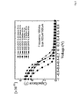
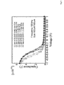
- FIGS. 2 and 3 are diagrams showing the voltage dependence of the capacitance of the semiconductor device according to the present invention.
- 2 shows a heat treatment FGA at 420 ° C. for 30 minutes in an atmosphere diluted with nitrogen
- FIG. 3 shows a heat treatment FGA at 420 ° C. for 30 minutes in an atmosphere in which hydrogen is diluted with nitrogen. It shows the voltage dependence of the capacitance.
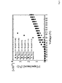
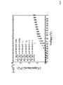
- FIG. 4 and 5 are diagrams showing the voltage dependence of 1 / (capacitance) 2 of the semiconductor device according to the present invention.
- 4 shows a heat treatment FGA at 420 ° C. for 30 minutes in an atmosphere diluted with nitrogen
- FIG. 5 shows a heat treatment FGA at 420 ° C. for 30 minutes in an atmosphere in which hydrogen is diluted with nitrogen.
- FIG. 6 is a diagram showing an effective work function of the semiconductor device according to the present invention.
- FIG. 6 it contains tetrakis (ethylmethylamino) titanium with a nitrogen to titanium ratio of 0.86 and ammonia, and contains 10.3% carbon formed by ALD (Atomic Layer Deposition).
- the effective work function of the titanium nitride film having a thickness of 5 nm was 4.78 eV before performing the heat treatment FGA at 420 ° C. for 30 minutes in an atmosphere in which hydrogen was diluted with nitrogen.
- a titanium nitride film containing 10.3% carbon formed by ALD (Atomic Layer Layer Deposition) using tetrakis (ethylmethylamino) titanium having a nitrogen to titanium ratio of 0.86 and ammonia having a thickness of 7 nm
- the effective work function was 4.84 eV before performing heat treatment FGA at 420 ° C. for 30 minutes in an atmosphere in which hydrogen was diluted with nitrogen.
- the semiconductor device has an effective work function in the vicinity of 4.8 eV as described above, if the nMOS and the pMOS are formed of the same gate electrode material in the CMOS device, the threshold value of the nMOS becomes remarkably high. The threshold is low.
- the function was 4.6 eV before heat treatment FGA at 420 ° C. for 30 minutes in an atmosphere diluted with nitrogen.
- the function was 4.68 eV before performing heat treatment FGA at 420 ° C. for 30 minutes in an atmosphere in which hydrogen was diluted with nitrogen.
- Titanium nitride film containing 4.9% carbon formed by ALD (Atomic Layer Layer Deposition) using tetrakis (ethylmethylamino) titanium having a nitrogen to titanium ratio of 1.1 and ammonia and having a thickness of 5 nm
- the effective work function was 4.44 eV before performing the heat treatment FGA at 420 ° C. for 30 minutes in an atmosphere in which hydrogen was diluted with nitrogen.
- a titanium nitride film having a thickness of 7 nm and containing 4.9% carbon formed by ALD (Atomic Layer Layer Deposition) using tetrakis (ethylmethylamino) titanium having a nitrogen to titanium ratio of 1.1 and ammonia.
- the effective work function was 4.69 eV before performing heat treatment FGA at 420 ° C. for 30 minutes in an atmosphere in which hydrogen was diluted with nitrogen.
- the effective work function may change depending on the ratio of nitrogen to titanium. Indicated.
- a gate oxide film formed on a silicon substrate and a gate electrode formed on the gate oxide film are provided, and the gate electrode is a laminated structure of a titanium nitride film containing carbon and a polycrystalline silicon film.
- the silicon substrate, the gate oxide film, the carbon-containing titanium nitride film, and the polycrystalline silicon film are heat treated at 350 ° C. or higher in an atmosphere containing hydrogen, so that the silicon midgap It was shown that an effective work function in the vicinity of a certain 4.6 eV can be obtained.
- the desired effective work function can be obtained by changing the ratio of nitrogen to titanium and the film thickness of the titanium nitride film containing carbon.
- the gate oxide film formed on the silicon substrate and the gate electrode formed on the gate oxide film are provided, and the gate electrode includes a titanium nitride film containing carbon and a polycrystalline silicon film.
- the silicon substrate, the gate oxide film, the titanium nitride film containing carbon, and the polycrystalline silicon film are heat treated at 350 ° C. or higher in an atmosphere containing hydrogen, so that the silicon mid The effective work function in the vicinity of the gap of 4.6 eV can be obtained.
- a desired effective work function can be obtained by changing the ratio of nitrogen to titanium in the titanium nitride film containing carbon and the film thickness.
Landscapes
- Electrodes Of Semiconductors (AREA)
Abstract
有機ガスを用いた原子層堆積を用いて、所望の実効仕事関数を有する半導体装置を提供することを課題とする。半導体装置は、シリコン基板(101)上に形成されたゲート酸化膜(102)と、ゲート酸化膜(102)上に形成されたゲート電極とを備える。ゲート電極は、炭素を含有する窒化チタン膜と多結晶シリコン膜との積層構造であって、シリコン基板(101)と、ゲート酸化膜と炭素を含有する窒化チタン膜(103)と、多結晶シリコン膜(104)とは、水素を含む雰囲気中で350℃以上で熱処理されたことにより、上記課題を解決する。
Description
本発明は半導体装置に関する。
近年、メタルゲート電極を用いたCMOSデバイス開発が行われている。メタルゲート電極を用いる場合には、トランジスタのしきい値電圧は、チャネル領域の不純物濃度とゲート電極の仕事関数で決定される。
従来のトランジスタでは、チャネル濃度を1017cm-3以下の低不純物濃度とし、ゲート材料の仕事関数を変えることによって、しきい値電圧を決定することが提案されている(例えば、特許文献1を参照)。
CMOSデバイスにおいて、nMOSとpMOSを同じゲート電極材料で形成するとき、nMOSとpMOSとのしきい値電圧を互いに等しくするため、ゲート電極材料の仕事関数は、シリコンのミッドギャップである4.6eV近傍であることが望ましい。
特許文献2には、チタン金属ターゲットを用いてアルゴンガス流量と窒素ガス流量の混合比を調節することにより形成された、PVD(Physical Vapor Deposition)であるスパッタリング法を用いて形成された窒化チタン上にスパッタリング法を用いてシリコンを堆積した構造を窒素雰囲気中で熱処理した後の実効仕事関数が開示されている。
本発明は、有機ガスを用いた原子層堆積によって、所望の実効仕事関数を持つ半導体装置を提供することを目的とする。
本発明の観点に係る半導体装置は、シリコン基板上に形成されたゲート酸化膜と、前記ゲート酸化膜上に形成されたゲート電極と、を備え、前記ゲート電極は、炭素を含有する窒化チタン膜と多結晶シリコン膜との積層構造であって、前記シリコン基板と、前記ゲート酸化膜と、前記炭素を含有する窒化チタン膜と、前記多結晶シリコン膜とは、水素を含む雰囲気中で350℃以上で熱処理されたものである、ことを特徴とする。
また、前記窒化チタン膜は、テトラキス(エチルメチルアミノ)チタニウムとアンモニアとを用いて形成されたものであることを特徴とする。
また、前記窒化チタン膜の、窒素とチタンの比は、0.8~1.2であることを特徴とする。
また、前記窒化チタン膜の膜厚は、4nm~8nmであることを特徴とする。
また、前記水素と窒素の混合ガス雰囲気中での熱処理前に、前記シリコン基板と前記ゲート酸化膜と前記炭素を含有する窒化チタン膜は、窒素雰囲気中で、900℃以上で熱処理をされることを特徴とする。
また、前記ゲート酸化膜は、800℃以上の酸素を含む雰囲気を用いて形成されたものであることを特徴とする。
また、前記多結晶シリコン膜上に窒化タンタル膜が形成されていることを特徴とする。
また、前記多結晶シリコン膜は、減圧化学気相堆積装置で形成されたものであることを特徴とする。
本発明によれば、有機ガスを用いた原子層堆積を用いて、所望の実効仕事関数を持つ半導体装置を提供することができる。
以下、本発明に係る半導体装置の実施形態を、図面を参照しながら詳細に説明する。
図1は、本発明に係る半導体装置の断面図である。
まず、6×1015cm-3のp型シリコン基板101を、1000℃の、酸素を窒素で希釈した雰囲気を用いて酸化することによって、膜厚5nmのゲート酸化膜102を形成した。
まず、6×1015cm-3のp型シリコン基板101を、1000℃の、酸素を窒素で希釈した雰囲気を用いて酸化することによって、膜厚5nmのゲート酸化膜102を形成した。
次に、テトラキス(エチルメチルアミノ)チタニウムとアンモニアとを用い、ALD(Atomic Layer Deposition)によって、三種類の窒化チタン膜103をゲート酸化膜102上に堆積した。窒化チタン膜103、ゲート酸化膜102の膜厚はそれぞれ5nm、7nmとした。テトラキス(エチルメチルアミノ)チタニウムは、有機ガスであるため、堆積された窒化チタン膜103中に炭素が残存する。X線光電子分光装置を用いて測定したところ、三種類の窒化チタン膜103での窒素とチタンの比は、それぞれ、0.86、1、1.1であった。また、三種類の窒化チタン膜103から、10.3%、8.4%、4.9%の炭素がそれぞれ検出された。
次に、減圧化学気相堆積装置(LPCVD装置)を用いて、窒化チタン膜103上に多結晶シリコン膜104を18nm堆積した。
次に、砒素を多結晶シリコン膜104に注入した。
次に、窒素雰囲気中で、1050℃、1秒の熱処理を行い、600℃、10分の熱処理を行った。
次に、窒化タンタルと、アルミニウムと、窒化タンタルとからなる積層膜105を堆積し、リソグラフィー技術とエッチング技術とを用いて、ゲート電極を形成した。
次に、容量の電圧依存性を測定した。
次に、水素を窒素で希釈した雰囲気中で、420℃、30分の熱処理FGA(Forming Gas Anneal)を行った。
次に、再び容量の電圧依存性を測定した。
図2と図3は、本発明に係る半導体装置の容量の電圧依存性を示す図である。図2は、水素を窒素で希釈した雰囲気中で420℃、30分の熱処理FGAを行う前、図3は、水素を窒素で希釈した雰囲気中で420℃、30分の熱処理FGAを行った後の容量の電圧依存性を示している。
また、図4と図5は、本発明に係る半導体装置の1/(容量)2の電圧依存性を示す図である。図4は、水素を窒素で希釈した雰囲気中で420℃、30分の熱処理FGAを行う前、図5は、水素を窒素で希釈した雰囲気中で420℃、30分の熱処理FGAを行った後の容量の1/(容量)2の電圧依存性を示している。
次に、図4と図5に示す1/(容量)2の電圧依存性のグラフを用いて、半導体装置の実効仕事関数を見積もった。図6は、本発明に係る半導体装置の実効仕事関数を示す図である。
図6に示されるように、窒素とチタンの比が0.86であるテトラキス(エチルメチルアミノ)チタニウムとアンモニアとを用い、ALD(Atomic Layer Deposition)によって形成された10.3%の炭素を含む窒化チタン膜の膜厚5nmの実効仕事関数は、水素を窒素で希釈した雰囲気中で420℃、30分の熱処理FGAを行う前に、4.78eVであった。
窒素とチタンの比が0.86であるテトラキス(エチルメチルアミノ)チタニウムとアンモニアとを用い、ALD(Atomic Layer Deposition)によって形成された10.3%の炭素を含む窒化チタン膜の膜厚7nmの実効仕事関数は、水素を窒素で希釈した雰囲気中で420℃、30分の熱処理FGAを行う前に、4.84eVであった。
このように半導体装置が4.8eV近傍の実効仕事関数を有する場合には、CMOSデバイスにおいて、nMOSとpMOSとを同じゲート電極材料で形成すると、nMOSのしきい値は著しく高くなり、pMOSのしきい値は低くなる。
水素を窒素で希釈した雰囲気中で420℃、30分の熱処理FGAを行ったところ、窒素とチタンの比が0.86であるテトラキス(エチルメチルアミノ)チタニウムとアンモニアとを用い、ALD(Atomic Layer Deposition)によって形成された10.3%の炭素を含む窒化チタン膜の膜厚5nm、7nmの実効仕事関数を、4.6eV近傍とすることができた。
窒素とチタンの比が1であるテトラキス(エチルメチルアミノ)チタニウムとアンモニアとを用い、ALD(Atomic Layer Deposition)によって形成された8.4%の炭素を含む窒化チタン膜の膜厚5nmの実効仕事関数は、水素を窒素で希釈した雰囲気中で420℃、30分の熱処理FGAを行う前に、4.6eVであった。
窒素とチタンの比が1であるテトラキス(エチルメチルアミノ)チタニウムとアンモニアとを用い、ALD(Atomic Layer Deposition)によって形成された8.4%の炭素を含む窒化チタン膜の膜厚7nmの実効仕事関数は、水素を窒素で希釈した雰囲気中で420℃、30分の熱処理FGAを行う前に、4.68eVであった。
水素を窒素で希釈した雰囲気中で420℃、30分の熱処理FGAを行ったところ、窒素とチタンの比が1であるテトラキス(エチルメチルアミノ)チタニウムとアンモニアとを用い、ALD(Atomic Layer Deposition)によって形成された8.4%の炭素を含む窒化チタン膜の膜厚5nmの実効仕事関数は、4.42eVとなった。
水素を窒素で希釈した雰囲気中で420℃、30分の熱処理FGAを行ったところ、窒素とチタンの比が1であるテトラキス(エチルメチルアミノ)チタニウムとアンモニアとを用い、ALD(Atomic Layer Deposition)によって形成された8.4%の炭素を含む窒化チタン膜の膜厚7nmの実効仕事関数は、4.6eVとなった。
窒素とチタンの比が1.1であるテトラキス(エチルメチルアミノ)チタニウムとアンモニアとを用い、ALD(Atomic Layer Deposition)によって形成された4.9%の炭素を含む窒化チタン膜の膜厚5nmの実効仕事関数は、水素を窒素で希釈した雰囲気中で420℃、30分の熱処理FGAを行う前に、4.44eVであった。
窒素とチタンの比が1.1であるテトラキス(エチルメチルアミノ)チタニウムとアンモニアとを用い、ALD(Atomic Layer Deposition)によって形成された4.9%の炭素を含む窒化チタン膜の膜厚7nmの実効仕事関数は、水素を窒素で希釈した雰囲気中で420℃、30分の熱処理FGAを行う前に、4.69eVであった。
水素を窒素で希釈した雰囲気中で420℃、30分の熱処理FGAを行ったところ、窒素とチタンの比が1.1であるテトラキス(エチルメチルアミノ)チタニウムとアンモニアとを用い、ALD(Atomic Layer Deposition)によって形成された4.9%の炭素を含む窒化チタン膜の膜厚5nmの実効仕事関数は、4.38eVとなった。
水素を窒素で希釈した雰囲気中で420℃、30分の熱処理FGAを行ったところ、窒素とチタンの比が1.1であるテトラキス(エチルメチルアミノ)チタニウムとアンモニアとを用い、ALD(Atomic Layer Deposition)によって形成された4.9%の炭素を含む窒化チタン膜の膜厚7nmの実効仕事関数は、4.57eVとなった。
以上から、水素を窒素で希釈した雰囲気中で420℃、30分の熱処理FGA後、窒化チタン膜の膜厚が7nmのとき、窒素とチタンの比が0.8~1.2の間で、実効仕事関数は4.6eV近傍となることが示された。
また、水素を窒素で希釈した雰囲気中で420℃、30分の熱処理FGA後、窒化チタン膜の膜厚が5nmのとき、実効仕事関数は、窒素とチタンの比に依存し、変化することが示された。
以上から、シリコン基板上に形成されたゲート酸化膜と、ゲート酸化膜上に形成されたゲート電極と、を備え、ゲート電極は、炭素を含有する窒化チタン膜と多結晶シリコン膜との積層構造であって、シリコン基板と、ゲート酸化膜と、炭素を含有する窒化チタン膜と、多結晶シリコン膜とは、水素を含む雰囲気中で350℃以上で熱処理されたことにより、シリコンのミッドギャップである4.6eV近傍の実効仕事関数とすることができることが示された。
また、炭素を含有する窒化チタン膜の、窒素とチタンの比と、膜厚とを変えることにより、所望の実効仕事関数とすることができることが示された。
上記実施形態によれば、シリコン基板上に形成されたゲート酸化膜と、ゲート酸化膜上に形成されたゲート電極と、を備え、ゲート電極は、炭素を含有する窒化チタン膜と多結晶シリコン膜の積層構造であって、シリコン基板と、ゲート酸化膜と炭素を含有する窒化チタン膜と、多結晶シリコン膜とは、水素を含む雰囲気中で350℃以上で熱処理されたことにより、シリコンのミッドギャップである4.6eV近傍の実効仕事関数とすることができる。
また、炭素を含有する窒化チタン膜の窒素とチタンの比と、膜厚とを変えることにより、所望の実効仕事関数とすることができる。
101.シリコン基板
102.ゲート酸化膜
103.窒化チタン膜
104.多結晶シリコン膜
105.窒化タンタル、アルミニウム、窒化タンタルの積層膜
102.ゲート酸化膜
103.窒化チタン膜
104.多結晶シリコン膜
105.窒化タンタル、アルミニウム、窒化タンタルの積層膜
Claims (8)
- シリコン基板上に形成されたゲート酸化膜と、
前記ゲート酸化膜上に形成されたゲート電極と、を備え、
前記ゲート電極は、炭素を含有する窒化チタン膜と多結晶シリコン膜との積層構造であって、
前記シリコン基板と、前記ゲート酸化膜と、前記炭素を含有する窒化チタン膜と、前記多結晶シリコン膜とは、水素を含む雰囲気中で350℃以上で熱処理されたものである、
ことを特徴とする半導体装置。 - 前記窒化チタン膜は、テトラキス(エチルメチルアミノ)チタニウムとアンモニアとを用いて形成されたものであることを特徴とする請求項1に記載の半導体装置。
- 前記窒化チタン膜の、窒素とチタンの比は、0.8~1.2であることを特徴とする請求項2に記載の半導体装置。
- 前記窒化チタン膜の膜厚は、4nm~8nmであることを特徴とする請求項2または3に記載の半導体装置。
- 前記水素と窒素の混合ガス雰囲気中での熱処理前に、前記シリコン基板と前記ゲート酸化膜と前記炭素を含有する窒化チタン膜は、窒素雰囲気中で、900℃以上で熱処理をされることを特徴とする請求項1乃至4のいずれか一項に記載の半導体装置。
- 前記ゲート酸化膜は、800℃以上の酸素を含む雰囲気を用いて形成されたものであることを特徴とする請求項1乃至5のいずれか一項に記載の半導体装置。
- 前記多結晶シリコン膜上に窒化タンタル膜が形成されていることを特徴とする請求項1に記載の半導体装置。
- 前記多結晶シリコン膜は、減圧化学気相堆積装置で形成されたものであることを特徴とする請求項1に記載の半導体装置。
Priority Applications (1)
| Application Number | Priority Date | Filing Date | Title |
|---|---|---|---|
| PCT/JP2013/080258 WO2015068264A1 (ja) | 2013-11-08 | 2013-11-08 | 半導体装置 |
Applications Claiming Priority (1)
| Application Number | Priority Date | Filing Date | Title |
|---|---|---|---|
| PCT/JP2013/080258 WO2015068264A1 (ja) | 2013-11-08 | 2013-11-08 | 半導体装置 |
Publications (1)
| Publication Number | Publication Date |
|---|---|
| WO2015068264A1 true WO2015068264A1 (ja) | 2015-05-14 |
Family
ID=53041065
Family Applications (1)
| Application Number | Title | Priority Date | Filing Date |
|---|---|---|---|
| PCT/JP2013/080258 Ceased WO2015068264A1 (ja) | 2013-11-08 | 2013-11-08 | 半導体装置 |
Country Status (1)
| Country | Link |
|---|---|
| WO (1) | WO2015068264A1 (ja) |
Citations (8)
| Publication number | Priority date | Publication date | Assignee | Title |
|---|---|---|---|---|
| JPH08274334A (ja) * | 1995-03-30 | 1996-10-18 | Samsung Electron Co Ltd | Mosトランジスタ及びその製造方法 |
| JP2006024894A (ja) * | 2004-07-05 | 2006-01-26 | Samsung Electronics Co Ltd | 高誘電率のゲート絶縁膜を有する半導体装置及びそれの製造方法 |
| JP2007113103A (ja) * | 2005-10-24 | 2007-05-10 | Tokyo Electron Ltd | 成膜方法、成膜装置及び記憶媒体 |
| JP2007150321A (ja) * | 2006-11-30 | 2007-06-14 | Toshiba Corp | 半導体装置の製造方法 |
| JP2010503224A (ja) * | 2006-09-06 | 2010-01-28 | インターナショナル・ビジネス・マシーンズ・コーポレーション | 低抵抗コンタクト構造体及びその製造方法 |
| JP2012231123A (ja) * | 2011-04-15 | 2012-11-22 | Hitachi Kokusai Electric Inc | 半導体装置、半導体装置の製造方法、基板処理システムおよびプログラム |
| JP2012253352A (ja) * | 2011-06-01 | 2012-12-20 | Asm Ip Holding B V | 高有効仕事関数で電極を堆積する方法 |
| JP2013051250A (ja) * | 2011-08-30 | 2013-03-14 | Elpida Memory Inc | 半導体装置及びその製造方法 |
-
2013
- 2013-11-08 WO PCT/JP2013/080258 patent/WO2015068264A1/ja not_active Ceased
Patent Citations (8)
| Publication number | Priority date | Publication date | Assignee | Title |
|---|---|---|---|---|
| JPH08274334A (ja) * | 1995-03-30 | 1996-10-18 | Samsung Electron Co Ltd | Mosトランジスタ及びその製造方法 |
| JP2006024894A (ja) * | 2004-07-05 | 2006-01-26 | Samsung Electronics Co Ltd | 高誘電率のゲート絶縁膜を有する半導体装置及びそれの製造方法 |
| JP2007113103A (ja) * | 2005-10-24 | 2007-05-10 | Tokyo Electron Ltd | 成膜方法、成膜装置及び記憶媒体 |
| JP2010503224A (ja) * | 2006-09-06 | 2010-01-28 | インターナショナル・ビジネス・マシーンズ・コーポレーション | 低抵抗コンタクト構造体及びその製造方法 |
| JP2007150321A (ja) * | 2006-11-30 | 2007-06-14 | Toshiba Corp | 半導体装置の製造方法 |
| JP2012231123A (ja) * | 2011-04-15 | 2012-11-22 | Hitachi Kokusai Electric Inc | 半導体装置、半導体装置の製造方法、基板処理システムおよびプログラム |
| JP2012253352A (ja) * | 2011-06-01 | 2012-12-20 | Asm Ip Holding B V | 高有効仕事関数で電極を堆積する方法 |
| JP2013051250A (ja) * | 2011-08-30 | 2013-03-14 | Elpida Memory Inc | 半導体装置及びその製造方法 |
Similar Documents
| Publication | Publication Date | Title |
|---|---|---|
| CN103681671B (zh) | 具有钨栅电极的半导体器件及其制造方法 | |
| CN103811326B (zh) | 用于中间隙半导体设备的金属栅极结构及其制造方法 | |
| US8932923B2 (en) | Semiconductor gate structure for threshold voltage modulation and method of making same | |
| US9281310B2 (en) | Semiconductor device including gate structure for threshold voltage modulation in transistors and method for fabricating the same | |
| US9013000B2 (en) | Semiconductor device and method of manufacturing the same | |
| JP5336814B2 (ja) | 半導体装置およびその製造方法 | |
| US8786031B2 (en) | Metal nitride film, semiconductor device using the metal nitride film, and manufacturing method of semiconductor device | |
| US8524554B2 (en) | Semiconductor device and method for fabricating the same | |
| US20180076199A1 (en) | Complimentary metal-oxide-semiconductor circuit having transistors with different threshold voltages and method of manufacturing the same | |
| JP2004241725A (ja) | 半導体装置およびその製造方法 | |
| TW201208041A (en) | Semiconductor device and manufacturing method thereof | |
| JP2008543050A (ja) | 半導体デバイス構造およびその方法 | |
| KR100775965B1 (ko) | 모스 트랜지스터 및 그 제조 방법 | |
| CN104979290B (zh) | Cmos器件结构及其制作方法 | |
| JP5960491B2 (ja) | 半導体装置およびその製造方法 | |
| KR100753558B1 (ko) | 씨모스 트랜지스터 및 그 제조 방법 | |
| JP2008258487A (ja) | 半導体装置の製造装置 | |
| WO2015068264A1 (ja) | 半導体装置 | |
| WO2015063840A1 (ja) | 半導体装置 | |
| KR102532520B1 (ko) | 문턱 전압이 제어된 반도체 소자 및 그 제조방법 | |
| US9437498B2 (en) | Method for the formation of different gate metal regions of MOS transistors | |
| Kamiyama et al. | Structural and Electrical Properties of Nitrogen-Incorporated MOCVD Hf-Silicate Gate Dielectrics Treated by Plasma Nitridation in an Ar∕ N2 Ambient | |
| JP5177980B2 (ja) | 半導体装置およびその製造方法 | |
| JP2009094227A (ja) | nチャネルMOSトランジスタおよびその製造方法、半導体装置 | |
| US10615041B2 (en) | Methods and materials for modifying the threshold voltage of metal oxide stacks |
Legal Events
| Date | Code | Title | Description |
|---|---|---|---|
| 121 | Ep: the epo has been informed by wipo that ep was designated in this application |
Ref document number: 13897115 Country of ref document: EP Kind code of ref document: A1 |
|
| NENP | Non-entry into the national phase |
Ref country code: DE |
|
| 122 | Ep: pct application non-entry in european phase |
Ref document number: 13897115 Country of ref document: EP Kind code of ref document: A1 |