WO2015053173A1 - 可変容量デバイスおよび通信装置 - Google Patents
可変容量デバイスおよび通信装置 Download PDFInfo
- Publication number
- WO2015053173A1 WO2015053173A1 PCT/JP2014/076505 JP2014076505W WO2015053173A1 WO 2015053173 A1 WO2015053173 A1 WO 2015053173A1 JP 2014076505 W JP2014076505 W JP 2014076505W WO 2015053173 A1 WO2015053173 A1 WO 2015053173A1
- Authority
- WO
- WIPO (PCT)
- Prior art keywords
- variable capacitance
- capacitance elements
- bias line
- elements
- wiring layer
- Prior art date
- Legal status (The legal status is an assumption and is not a legal conclusion. Google has not performed a legal analysis and makes no representation as to the accuracy of the status listed.)
- Ceased
Links
Images



Classifications
-
- H—ELECTRICITY
- H01—ELECTRIC ELEMENTS
- H01Q—ANTENNAS, i.e. RADIO AERIALS
- H01Q7/00—Loop antennas with a substantially uniform current distribution around the loop and having a directional radiation pattern in a plane perpendicular to the plane of the loop
- H01Q7/005—Loop antennas with a substantially uniform current distribution around the loop and having a directional radiation pattern in a plane perpendicular to the plane of the loop with variable reactance for tuning the antenna
-
- H—ELECTRICITY
- H01—ELECTRIC ELEMENTS
- H01G—CAPACITORS; CAPACITORS, RECTIFIERS, DETECTORS, SWITCHING DEVICES, LIGHT-SENSITIVE OR TEMPERATURE-SENSITIVE DEVICES OF THE ELECTROLYTIC TYPE
- H01G17/00—Structural combinations of capacitors or other devices covered by at least two different main groups of this subclass with other electric elements, not covered by this subclass, e.g. RC combinations
-
- H—ELECTRICITY
- H01—ELECTRIC ELEMENTS
- H01G—CAPACITORS; CAPACITORS, RECTIFIERS, DETECTORS, SWITCHING DEVICES, LIGHT-SENSITIVE OR TEMPERATURE-SENSITIVE DEVICES OF THE ELECTROLYTIC TYPE
- H01G7/00—Capacitors in which the capacitance is varied by non-mechanical means; Processes of their manufacture
- H01G7/06—Capacitors in which the capacitance is varied by non-mechanical means; Processes of their manufacture having a dielectric selected for the variation of its permittivity with applied voltage, i.e. ferroelectric capacitors
Definitions
- the present invention relates to a variable capacitance device and a communication apparatus using the same.
- the paraelectric strontium titanate thin film and the ferroelectric strontium barium titanate thin film have a higher dielectric constant than the SiO 2 thin film and SiN thin film used in the semiconductor process. For this reason, it is considered that the material is suitable for reducing the circuit area.
- This thin film having a high dielectric constant is characterized in that the capacity decreases with the applied DC voltage.
- a device using such a thin film feature as an element is a variable capacitance device.
- this variable capacitance device a plurality of variable capacitance elements formed so as to sandwich the thin film as described above between conductor layers are connected in series, and one end of each variable capacitance element is a terminal for applying a control voltage And the other end connected to a terminal for grounding to the ground.
- the control voltage when the control voltage is increased, the capacitance is reduced by the action of the thin film described above.
- Such a variable capacitance device includes at least one variable capacitance element, and a wiring portion having an inductor component and a resistance component, and a wiring portion for applying a DC voltage thereto.
- the Q value determined by (Quality Factor) has frequency characteristics.
- a circuit including a capacitance and an inductance tends to decrease the resonance frequency of the circuit as the capacitance increases.
- the frequency characteristic regarding the Q value of the variable capacitance device is not always appropriate for the frequency band of the signal passing through the variable capacitance device.
- the efficiency of the circuit in which the variable capacitance device is used is greatly reduced.
- an object of the present invention is to increase the Q value of a variable capacitance device in a frequency band to be used, according to one aspect.
- the variable capacitance device includes (A) a first signal line including a plurality of first variable capacitance elements connected in series, and (B) a plurality of second variable capacitance elements connected in series. (C) a first bias line for applying a first DC voltage to each of the plurality of first variable capacitance elements and the plurality of second variable capacitance elements; D) a second bias line for applying a second DC voltage to each of the plurality of first variable capacitance elements and the plurality of second variable capacitance elements. Then, at least one part of the first bias line and the second bias line passes between two adjacent first variable capacitance elements among the plurality of first variable capacitance elements. Be placed. *
- the Q value can be increased by introducing a plurality of signal lines.
- the entire signal line extends in the horizontal direction, but the variable capacitance elements included in the signal line are stacked in the vertical direction, so that there is an empty space between the variable capacitance elements.
- the bias line is routed using this space, space utilization efficiency is high and a small device can be formed.
- the first DC voltage is, for example, a control voltage
- the second DC voltage is, for example, 0 V (ground). *
- first bias line and the second bias line described above is provided in each of two adjacent first variable capacitance elements among the plurality of first variable capacitance elements. You may make it form in the same layer as any one of the two electrode layers contained. In this way, it is not necessary to form an additional conductor layer for the bias line, so that an increase in cost can be suppressed.
- the number of the first variable capacitance elements described above is 4 or more
- the number of the second variable capacitance elements is 4 or more
- a part of the first bias line includes a plurality of first variable capacitors.
- the second bias line is arranged so as to pass between two adjacent first variable capacitance elements among the plurality of second variable capacitance elements, and a part of the second bias line is disposed between the two second variable capacitance elements adjacent to each other.
- the relative positions of the two variable capacitance elements may be different. In this way, it is possible to route the bias line with higher space utilization efficiency. *
- first bias line and a part of the second bias line described above are included in each of two adjacent first variable capacitors among the plurality of first variable capacitors. It may be formed of the same layer as any one of the electrode layers. In this way, an increase in manufacturing cost can be suppressed.
- first bias line may be formed in the same layer as the other layer of the two electrode layers. This is to avoid crossing the bias lines.
- the Q value of the variable capacitance device in the frequency band to be used can be increased.
- FIG. 1 is a diagram illustrating a basic equivalent circuit of a circuit included in a variable capacitance device.
- FIG. 2 is a diagram illustrating a configuration example of a variable capacitance device.
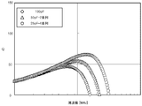
- FIG. 3 is a diagram illustrating an example of the frequency characteristic of the Q value.
- FIG. 4 is a plan view of the variable capacitance device according to the first embodiment.
- FIG. 5 is a diagram showing an AA ′ cross section of the variable capacitance device according to the first embodiment.
- FIG. 6 is a plan view of the variable capacitance device when the number of signal lines is three.
- FIG. 7 is a diagram illustrating a configuration example of a variable capacitance device when n signal lines are provided.
- FIG. 1 is a diagram illustrating a basic equivalent circuit of a circuit included in a variable capacitance device.
- FIG. 2 is a diagram illustrating a configuration example of a variable capacitance device.
- FIG. 3 is a diagram illustrating an example of the frequency
- FIG. 8 is a plan view of the variable capacitance device according to the second embodiment.
- FIG. 9 is a diagram showing a BB ′ cross section of the variable capacitance device according to the second embodiment.
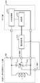
- FIG. 10 is a schematic diagram illustrating a communication apparatus according to the third embodiment.
- FIG. 1 shows a basic equivalent circuit of a circuit formed in the variable capacitance device according to the present embodiment. *
- the circuit for the variable capacitance device includes variable capacitance elements C1 to C4 and resistors R1 to R5 connected in series.
- the variable capacitance elements C1 to C4 are variable capacitance elements whose capacitance value decreases as the voltage applied to both ends thereof increases.
- the variable capacitance elements C1 to C4 are formed of a BST ((Ba, Sr) TiO 3 ) thin film.
- the resistors R1 to R5 are resistors for preventing high frequency signal leakage.
- the lines of the variable capacitance elements C1 to C4 are referred to as signal lines.
- One ends of the resistors R1 to R3 are connected to a terminal for connecting to the ground.
- the other end of the resistor R1 is connected to one end of the variable capacitor C1
- the other end of the resistor R2 is connected to one ends of the variable capacitors C2 and C3
- the other end of the resistor R3 is the variable capacitor C4. It is connected to one end.
- one ends of the resistors R4 and R5 are connected to a terminal for applying a control voltage.
- the other end of the resistor R4 is connected to the other ends of the variable capacitance elements C1 and C2, and the other end of the resistor R5 is connected to the other ends of the variable capacitance elements C3 and C4.
- the ground side wiring including the resistors R1 to R3 and the control voltage applying wiring including the resistors R4 and R5 are referred to as bias lines. *
- the Q value is increased by providing a plurality of signal lines in parallel in one variable capacitance device.
- the capacitance value C of each of the variable capacitance elements C1 to C4 when there is one signal line is C / 2 when two signal lines are used, and C / 3 when three signal lines are used.
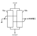
- the circuit shown in FIG. 1 is represented as a box as shown in FIG.
- a circuit 10a and a circuit 10b are provided in parallel.
- the ground side terminal and the control voltage application terminal are connected by wiring from the side surfaces of the circuits 10a and 10b, so that the wiring straddling the circuits 10a and 10b. Will be done.
- the device size is increased and the wiring layer is increased, resulting in an increase in cost. Resulting in. *
- FIG. 3 shows the frequency characteristics of the Q value in the case where four are provided and the combined capacitance of the variable capacitance elements C1 to C4 in one signal line is 25 pF.
- the horizontal axis represents frequency
- the vertical axis represents Q value.
- FIG. 4 shows a plan view of a variable capacitance device having two signal lines as an example.
- FIG. 4 only the main parts are shown, so that the substrate and other non-main parts are omitted.
- the first signal line includes, in order from the upper layer, wiring layers 101a to 101c, upper electrodes 103a to 103d, a dielectric layer formed under each of the upper electrodes 103a to 103d, a lower electrode 102a, 102b.
- the variable capacitance elements are formed by the number of the upper electrodes 103a and 103d.
- the wiring layer 101a is connected to the input-side terminal 122, and the wiring layer 101c is connected to the output-side terminal 121. *
- the lower electrode 102a is connected to the control voltage application terminal 123 via the resistance film 104a, and the lower electrode 102b is connected to the control voltage application terminal 123 via the resistance film 104b.
- the wiring layer 101a is connected to the ground terminal 124 through the resistance film 104c and the wiring layer 105 of the bias line.
- the wiring layer 101b is connected to the ground terminal 124 through the resistance film 104d and the wiring layer 105 of the bias line.
- the wiring layer 101c is connected to the ground terminal 124 through the resistance film 104e and the wiring layers 105, 108, and 107 of the bias line.
- the second signal line includes, in order from the upper layer, wiring layers 111a to 111c, upper electrodes 113a to 113d, a dielectric layer formed under each of the upper electrodes 113a to 113d, and a lower electrode. 112a and 112b.
- the wiring layer 111a is connected to the input-side terminal 122
- the wiring layer 111c is connected to the output-side terminal 121. *
- the lower electrode 112a is connected to a control voltage application terminal 123 via a resistance film 114a and a wiring layer 106 of a bias line.
- the lower electrode 112b is connected to the control voltage application terminal 123 via the resistance film 114b and the wiring layer 106 of the bias line.
- the wiring layer 111a is connected to the ground terminal 124 through the resistance film 114c and the wiring layer 116 of the bias line.
- the wiring layer 111b is connected to the ground terminal 124 through the resistance film 114d.
- the wiring layer 111c is connected to the ground terminal 124 through the resistance film 114e and the wiring layer 117 of the bias line.
- the terminal 123 for applying the control voltage cannot be connected to the second signal line unless it extends over the first signal line.
- the ground terminal 124 cannot be connected to the first signal line unless it extends over the second signal line.
- a part of the wiring layer 106 of the signal line is disposed so as to pass between the variable capacitance element including the upper electrode 103c and the variable capacitance element including the upper electrode 103d. Further, since the wiring layer 106 and the wiring layers 101a to 101c and 111a to 111c are formed in the same layer, the number of wiring layers does not increase, so that an increase in cost is suppressed. The vacant space is effectively utilized. *
- a part of the signal line wiring layer 105 is disposed so as to pass between the variable capacitance element including the upper electrode 113a and the variable capacitance element including the upper electrode 113b. Further, since the wiring layer 105 is formed in the same layer as the wiring layers 101a to 101c and 111a to 111c, the number of wiring layers does not increase, so that an increase in cost is suppressed. The vacant space is effectively utilized. *
- variable capacitance elements are included in one signal line, and the wiring layers 101a to 101c are divided into three, so that there are two spaces through which the wiring layer 106 can pass.
- the wirings 111a to 111c are divided into three, there are two spaces through which the wiring layer 105 can pass. Therefore, two spaces existing on the same line may be used, but the area of the entire device becomes large. Therefore, in this embodiment, from the input side terminal 122 or the output side terminal 121 in the signal line. Spaces having different distances (also referred to as relative positions from the reference position) are used. *
- the wiring layer 105 connected to the ground terminal 124 intersects the wiring layer 106 connected to the control voltage application terminal 123, the same as the lower electrodes 102a and 102b and 112a and 112b.
- a wiring layer 108 is formed, and the wiring layer 105 is connected to the wiring layer 107 in the same layer as the wiring layer 105 through the wiring layer 108.
- FIG. 5 shows a cross-sectional view taken along the line AA 'in FIG.
- An insulating layer 134 is formed over the substrate 133, and lower electrodes 102 a and 102 b, a wiring layer 135 a connected to the terminal 122, and a wiring layer 135 b connected to the terminal 121 are formed over the insulating layer 134. Is done.
- a dielectric layer 109a and an upper electrode 103a, and a dielectric layer 109b and an upper electrode 103b are formed on the lower electrode 102a.
- a dielectric layer 109c and an upper electrode 103c, and a dielectric layer 109d and an upper electrode 103d are formed on the lower electrode 102b.
- wiring layers 101a to 101c and a wiring layer 106 that is the same layer as the wiring layers 101a to 101c are formed on the upper portion thereof.
- an interlayer insulating film 136 is formed below the wiring layers 101a to 101c.
- a protective film 137 is formed above the wiring layers 101a to 101c.
- the substrate 133 is, for example, a silicon substrate or a single crystal substrate such as sapphire.
- the lower electrode 102 layer, the dielectric layer 109, and the upper electrode 103 layer are sequentially formed on almost the entire surface of the substrate 133. After the formation of these layers, the upper electrode 103, the dielectric layer 109, and the lower electrode 102 are sequentially etched into a predetermined shape.
- a material having a high melting point is used for the layer of the lower electrode 102. Specifically, it consists of metal materials, such as Pt and Pd. *
- a dielectric layer is formed by sputtering.
- heat treatment may be performed at a temperature of 400 to 700 ° C. for about 5 to 90 minutes in the atmosphere or in an atmosphere of nitrogen or oxygen in order to stabilize or improve the leakage current characteristics of the capacitor.
- the thickness of the lower electrode layer 102 be thick in consideration of the resistance component of the capacitance.
- the dielectric layer 109 is preferably a high dielectric constant dielectric layer made of perovskite oxide crystal particles containing at least Ba, Sr, and Ti.
- the dielectric layer 109 is formed on the surface of the lower electrode 102. *
- the thickness of the upper electrode 103 does not have a great influence on the resistance of the element as compared with the lower electrode 102, and therefore it does not need to be considered much, but is about 0.1 to 10 ⁇ m as a guide. *
- the bias line connected to the ground terminal 124 includes the wiring layer 105 and the resistance film 104 which is a thin film resistor, and is electrically connected to the upper electrode 103.
- the control voltage application terminal 123 is also electrically connected to the lower electrode 102 via the wiring layer 106 and the resistance film 104 in the same manner.
- the wiring layers 101 and 106 are formed by forming a lower electrode 102 layer, a dielectric layer 109 and an upper electrode 103 layer, and then forming a new film after forming an interlayer insulating film 136.
- a material of the thin film resistor constituting the resistance film 104 a material having a specific resistance of 1 m ⁇ cm or more is desirable.
- Tantalum nitride, TaSiN, and Ta—Si—O are effective as specific materials for the thin film resistor for such required values.
- a thin film resistor having a desired composition ratio and resistivity can be formed by a reactive sputtering method by using Ta and SiN as targets and adding nitrogen to the atmosphere.
- etching process such as reactive ion etching (RIE) is performed using the resist thin film as a mask.
- interlayer insulating film 136 As the interlayer insulating film 136, polyimide which is an organic insulating film, sputtered SiO 2 .Al 2 O 3 film which is an inorganic insulating film, CVD-SiO 2 , or a laminated film thereof is used.
- the interlayer insulating film 136 is formed by patterning, formation of signal line wiring layers 101a to 101c for connecting the input-side terminal 122 and the output-side terminal 121 and the variable capacitance element in series, a control voltage application terminal 123, The wiring layer 106 of the bias line that connects the ground terminal 124 via the resistance film 104 is formed.
- As a material for the wiring layers 101a to 101c and 106 Cu, Al or the like having a low resistance is suitable. The thickness is about 0.1 ⁇ m to 20 ⁇ m. *
- a protective film 137 for moisture resistance is formed except for regions where the terminals 121 to 124 are formed.
- the protective film 137 is sputtered SiO 2 or CVD-SiO 2 that is an inorganic insulating film, or a polyimide film that is an organic insulating film.
- the number of signal lines is two.
- the layout is as shown in FIG. Since the basic layout is the same as that shown in FIG. 4, detailed description is omitted, but the wiring layer 206 of the bias line for applying the control voltage has the second and third signal lines from the top. Therefore, it is longer than FIG.
- the wiring layer 205 of the bias line for ground is also longer than that in FIG. 4 because of the second and third signal lines from the bottom.
- a part of the wiring layers 207a and 207b are formed in the same layer as the lower electrode so that the wiring layers 205 and 206 do not intersect with each other, and are connected to the wiring layer 205 and the wiring layers 208a and 208b. . *
- the bias line is appropriately routed in the variable capacitance device, and the variable capacitance elements in each signal line function.
- FIG. 2 In the first embodiment, an example in which four variable capacitance elements are provided in one signal line is shown.
- the number of variable capacitance elements may be any number. However, in general, an even number of variable capacitance elements of 2 or more are often provided. If the number is four or more, as described in the first embodiment, two or more spaces for passing the bias line can be created, so that two bias lines for control voltage application and ground connection are passed. be able to.
- two variable capacitance elements are included in one signal line, there is only one space for passing the bias line, and one bias line is formed in the same layer as the lower electrode. Become. Such a case is shown in FIG. *
- the lower wiring layer 306 of the bias line connected to the terminal 323 for applying the control voltage is formed in the same layer as the lower electrode.
- the first signal line is exceeded, it is connected to the wiring layer 307 formed in the same layer as the upper wiring layers 301a and 311a, and the wiring layer 307 further has a lower portion for the second signal line from the top.
- the electrode is connected via a resistance film.
- the bias line wiring layer 305 connected to the ground terminal 324 extends between the variable capacitance elements in the second signal line from the top, and the upper wiring layer in the first signal line from the top. It connects to 301a etc. via the resistance film.
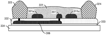
- FIG. 9 shows a cross-sectional view taken along line BB ′ in FIG.
- the lower wiring layer 306 is formed on the insulating layer 333 formed on the substrate 334 so as to pass through the upper wiring layer 301a in the first signal line.
- the lower wiring layer 306 is connected to the terminal 323 and further connected to the wiring layer 307.
- An interlayer insulating film 332 is formed between the lower wiring layer 306 and the upper wiring layer 301a.
- the interlayer insulating film 332 is a sputtered SiO 2 .Al 2 O 3 film, CVD-SiO 2 , or a laminated film thereof, which is an inorganic insulating film.
- the protective film 331 is an inorganic insulating film such as sputtered SiO 2 or CVD-SiO 2 , or an organic insulating film such as a polyimide film.
- FIG. 10 shows a configuration example of a communication apparatus according to the present embodiment.
- This communication apparatus includes an RFIC (Radio Frequency Integrated Circuit) unit 500, a voltage control unit 410, and a resonant antenna circuit module unit 400.
- RFIC Radio Frequency Integrated Circuit
- the resonant antenna circuit module unit 400 includes an inductor L and a series connection circuit of a DC cut capacitor CDC1, a variable capacitance device VC, and a DC cut capacitor CDC2 connected in parallel with the inductor L to form a resonant antenna.
- the resonant frequency of the resonant antenna circuit module unit 400 is determined by the inductor L and the capacitance of the series connection circuit.
- the RFIC unit 500 includes a signal processing unit 520 and a calculation unit 510.
- the signal processing unit 520 performs processing for communication such as demodulating the high-frequency signal RF received by the resonant antenna circuit module unit 400.
- the calculation unit 510 controls the operation timing of the signal processing unit 520 and performs a process of instructing the voltage control unit 410 at a predetermined timing to the bias voltage to the DC1 terminal or DC2 terminal.
- the calculation unit 510 also instructs the voltage control unit 410 also the bias voltage to be applied to the variable capacitance device VC. *
- variable capacitance device VC of the resonant antenna circuit module unit 400 for example, a variable capacitance device having a plurality of signal lines as shown in FIG. 4 or FIG. 6 is used. *
- variable capacitance device having a plurality of signal lines has a higher frequency at which the Q value is maximized compared to a variable capacitance device having the same combined capacitance and a single signal line. Therefore, the communication apparatus according to the present embodiment is higher in efficiency than a communication apparatus using a variable capacitance device having the same combined capacity and one signal line.
- the present invention is not limited to this.
- the upper and lower relationships between the wiring layers 101 and 111 and the lower electrodes 102 and 112 in FIG. 4 may be interchanged.
- the relationship of the layers of the bias line is also changed in accordance with the above-mentioned purpose.
- the positions of the ground terminal and the control voltage application terminal may be interchanged. Further, since the capacitance of the variable capacitance element changes depending on the applied voltage difference, a voltage other than 0 V may be applied to the ground terminal, and a different voltage may be applied to the control voltage application terminal accordingly. .
Landscapes
- Engineering & Computer Science (AREA)
- Power Engineering (AREA)
- Microelectronics & Electronic Packaging (AREA)
- Semiconductor Integrated Circuits (AREA)
- Fixed Capacitors And Capacitor Manufacturing Machines (AREA)
Abstract
Description
インの配線層117とを介して、グランド用の端子124と接続されている。
を増加させることがないので、コストの上昇が抑制されている。
Claims (6)
- 直列に接続された複数の第1の可変容量素子を含む第1のシグナルラインと、 直列に接続された複数の第2の可変容量素子を含む第2のシグナルラインと、 前記複数の第1の可変容量素子及び前記複数の第2の可変容量素子の各々に第1の直流電圧を印加するための第1のバイアスラインと、 前記複数の第1の可変容量素子及び前記複数の第2の可変容量素子の各々に第2の直流電圧を印加するための第2のバイアスラインと、 を有し、 前記第1のバイアスラインと前記第2のバイアスラインとのうち少なくともいずれかの一部分が、前記複数の第1の可変容量素子のうち隣接する2つの第1の可変容量素子の間を通過するように配置される 可変容量デバイス。
- 前記第1のバイアスラインと前記第2のバイアスラインとのうち少なくともいずれかの一部分が、 前記複数の第1の可変容量素子のうち隣接する2つの第1の可変容量素子の各々に含まれる2つの電極層のいずれか一方と同一層で形成される 請求項1記載の可変容量デバイス。
- 前記第1の可変容量素子の数が4以上であり、 前記第2の可変容量素子の数が4以上であり、 前記第1のバイアスラインの一部分が、前記複数の第1の可変容量素子のうち隣接する2つの第1の可変容量素子の間を通過するように配置され、 前記第2のバイアスラインの一部分が、前記複数の第2の可変容量素子のうち隣接する2つの第2の可変容量素子の間を通過するように配置され、 前記複数の第1の可変容量素子における、前記2つの第1の可変容量素子の相対位置と、前記複数の第2の可変容量素子における、前記2つの第2の可変容量素子の相対位置とが、異なっている 請求項1記載の可変容量デバイス。
- 前記第1のバイアスラインの一部分及び前記第2のバイアスラインの一部分が、 前記複数の第1の可変容量素子のうち隣接する2つの第1の可変容量素子の各々に含まれる2つの電極層のいずれか一方と同一層で形成される 請求項3記載の可変容量デバイス。
- 前記第1のバイアスラインの他の一部分が、 前記2つの電極層の他方の層と同一層で形成される 請求項4記載の可変容量デバイス。
- 共振アンテナを形成するインダクタと、前記ンダクタと並列に接続される可変容量デバイスと、を有する通信装置であって、前記可変容量デバイスが、請求項1~5に記載の可変容量デバイスである 通信装置。
Priority Applications (2)
| Application Number | Priority Date | Filing Date | Title |
|---|---|---|---|
| US15/027,425 US10044105B2 (en) | 2013-10-07 | 2014-10-03 | Variable capacitance device and communication apparatus |
| JP2015541547A JP6416102B2 (ja) | 2013-10-07 | 2014-10-03 | 可変容量デバイスおよび通信装置 |
Applications Claiming Priority (2)
| Application Number | Priority Date | Filing Date | Title |
|---|---|---|---|
| JP2013-210026 | 2013-10-07 | ||
| JP2013210026 | 2013-10-07 |
Publications (1)
| Publication Number | Publication Date |
|---|---|
| WO2015053173A1 true WO2015053173A1 (ja) | 2015-04-16 |
Family
ID=52812989
Family Applications (1)
| Application Number | Title | Priority Date | Filing Date |
|---|---|---|---|
| PCT/JP2014/076505 Ceased WO2015053173A1 (ja) | 2013-10-07 | 2014-10-03 | 可変容量デバイスおよび通信装置 |
Country Status (3)
| Country | Link |
|---|---|
| US (1) | US10044105B2 (ja) |
| JP (1) | JP6416102B2 (ja) |
| WO (1) | WO2015053173A1 (ja) |
Cited By (1)
| Publication number | Priority date | Publication date | Assignee | Title |
|---|---|---|---|---|
| JP2017098343A (ja) * | 2015-11-19 | 2017-06-01 | 太陽誘電株式会社 | 可変容量デバイス及びアンテナ回路 |
Citations (4)
| Publication number | Priority date | Publication date | Assignee | Title |
|---|---|---|---|---|
| JP2006196871A (ja) * | 2004-12-15 | 2006-07-27 | Kyocera Corp | 薄膜コンデンサおよび可変容量コンデンサならびに電子部品 |
| WO2008001914A1 (fr) * | 2006-06-29 | 2008-01-03 | Kyocera Corporation | Ensemble de condensateurs à capacitance variable, dispositif d'ensemble de condensateurs à capacitance variable et module |
| JP2008211064A (ja) * | 2007-02-27 | 2008-09-11 | Kyocera Corp | 可変容量コンデンサアレイ及び可変容量コンデンサリレー |
| WO2013061985A1 (ja) * | 2011-10-26 | 2013-05-02 | 株式会社村田製作所 | 可変容量素子および高周波デバイス |
Family Cites Families (5)
| Publication number | Priority date | Publication date | Assignee | Title |
|---|---|---|---|---|
| US6674321B1 (en) | 2001-10-31 | 2004-01-06 | Agile Materials & Technologies, Inc. | Circuit configuration for DC-biased capacitors |
| JP4060746B2 (ja) * | 2003-04-18 | 2008-03-12 | 株式会社ヨコオ | 可変同調型アンテナおよびそれを用いた携帯無線機 |
| JP4566012B2 (ja) | 2005-01-13 | 2010-10-20 | 京セラ株式会社 | 可変容量コンデンサ,回路モジュールおよび通信装置 |
| WO2007145259A1 (ja) * | 2006-06-13 | 2007-12-21 | Kyocera Corporation | 可変容量回路 |
| JP5666123B2 (ja) | 2009-12-03 | 2015-02-12 | デクセリアルズ株式会社 | 可変容量デバイス |
-
2014
- 2014-10-03 JP JP2015541547A patent/JP6416102B2/ja not_active Expired - Fee Related
- 2014-10-03 WO PCT/JP2014/076505 patent/WO2015053173A1/ja not_active Ceased
- 2014-10-03 US US15/027,425 patent/US10044105B2/en not_active Expired - Fee Related
Patent Citations (4)
| Publication number | Priority date | Publication date | Assignee | Title |
|---|---|---|---|---|
| JP2006196871A (ja) * | 2004-12-15 | 2006-07-27 | Kyocera Corp | 薄膜コンデンサおよび可変容量コンデンサならびに電子部品 |
| WO2008001914A1 (fr) * | 2006-06-29 | 2008-01-03 | Kyocera Corporation | Ensemble de condensateurs à capacitance variable, dispositif d'ensemble de condensateurs à capacitance variable et module |
| JP2008211064A (ja) * | 2007-02-27 | 2008-09-11 | Kyocera Corp | 可変容量コンデンサアレイ及び可変容量コンデンサリレー |
| WO2013061985A1 (ja) * | 2011-10-26 | 2013-05-02 | 株式会社村田製作所 | 可変容量素子および高周波デバイス |
Cited By (1)
| Publication number | Priority date | Publication date | Assignee | Title |
|---|---|---|---|---|
| JP2017098343A (ja) * | 2015-11-19 | 2017-06-01 | 太陽誘電株式会社 | 可変容量デバイス及びアンテナ回路 |
Also Published As
| Publication number | Publication date |
|---|---|
| US10044105B2 (en) | 2018-08-07 |
| JPWO2015053173A1 (ja) | 2017-03-09 |
| JP6416102B2 (ja) | 2018-10-31 |
| US20160254599A1 (en) | 2016-09-01 |
Similar Documents
| Publication | Publication Date | Title |
|---|---|---|
| US7973246B2 (en) | Electronic component | |
| JP5159776B2 (ja) | キャパシタ,共振器、フィルタ装置,通信装置、並びに電気回路 | |
| US8207567B2 (en) | Metal-oxide-metal structure with improved capacitive coupling area | |
| US20020066919A1 (en) | BEOL decoupling capacitor | |
| US10424440B2 (en) | Capacitor having an auxiliary electrode | |
| JPWO2008001914A1 (ja) | 可変容量コンデンサアレイ,可変容量コンデンサアレイ装置及び回路モジュール | |
| JP4502609B2 (ja) | 可変コンデンサ | |
| JP6451893B2 (ja) | 容量素子 | |
| US20190123131A1 (en) | Small-gap coplanar tunable capacitors and methods for manufacturing thereof | |
| CN100437849C (zh) | 薄膜电容器及其制造方法 | |
| US7002435B2 (en) | Variable capacitance circuit, variable capacitance thin film capacitor and radio frequency device | |
| US9000866B2 (en) | Varactor shunt switches with parallel capacitor architecture | |
| JP4518013B2 (ja) | 電子部品 | |
| JP4749052B2 (ja) | 可変容量コンデンサ,回路モジュールおよび通信装置 | |
| JP6416102B2 (ja) | 可変容量デバイスおよび通信装置 | |
| JP4566012B2 (ja) | 可変容量コンデンサ,回路モジュールおよび通信装置 | |
| US7009276B2 (en) | Thin film capacitor, thin film capacitor array and electronic component | |
| US9590677B2 (en) | Variable capacitance device and antenna apparatus | |
| JP4651355B2 (ja) | 可変容量コンデンサ | |
| JP2008211064A (ja) | 可変容量コンデンサアレイ及び可変容量コンデンサリレー | |
| JP3958173B2 (ja) | 可変コンデンサ装置 | |
| JP2008277996A (ja) | 可変容量コンデンサ、フィルタ回路 | |
| JP4535817B2 (ja) | 薄膜コンデンサ、薄膜コンデンサアレイおよび電子部品 | |
| JP4493405B2 (ja) | 可変コンデンサ,回路モジュールおよび通信装置 | |
| JP2002329788A (ja) | 可変コンデンサ |
Legal Events
| Date | Code | Title | Description |
|---|---|---|---|
| 121 | Ep: the epo has been informed by wipo that ep was designated in this application |
Ref document number: 14852815 Country of ref document: EP Kind code of ref document: A1 |
|
| ENP | Entry into the national phase |
Ref document number: 2015541547 Country of ref document: JP Kind code of ref document: A |
|
| WWE | Wipo information: entry into national phase |
Ref document number: 15027425 Country of ref document: US |
|
| NENP | Non-entry into the national phase |
Ref country code: DE |
|
| 122 | Ep: pct application non-entry in european phase |
Ref document number: 14852815 Country of ref document: EP Kind code of ref document: A1 |