WO2015050141A1 - 半導体放射線検出器、それを用いた核医学診断装置、および半導体放射線検出器の製造方法 - Google Patents
半導体放射線検出器、それを用いた核医学診断装置、および半導体放射線検出器の製造方法 Download PDFInfo
- Publication number
- WO2015050141A1 WO2015050141A1 PCT/JP2014/076195 JP2014076195W WO2015050141A1 WO 2015050141 A1 WO2015050141 A1 WO 2015050141A1 JP 2014076195 W JP2014076195 W JP 2014076195W WO 2015050141 A1 WO2015050141 A1 WO 2015050141A1
- Authority
- WO
- WIPO (PCT)
- Prior art keywords
- semiconductor
- less
- radiation detector
- full width
- half maximum
- Prior art date
- Legal status (The legal status is an assumption and is not a legal conclusion. Google has not performed a legal analysis and makes no representation as to the accuracy of the status listed.)
- Ceased
Links
Images


Classifications
-
- A—HUMAN NECESSITIES
- A61—MEDICAL OR VETERINARY SCIENCE; HYGIENE
- A61B—DIAGNOSIS; SURGERY; IDENTIFICATION
- A61B6/00—Apparatus or devices for radiation diagnosis; Apparatus or devices for radiation diagnosis combined with radiation therapy equipment
- A61B6/42—Arrangements for detecting radiation specially adapted for radiation diagnosis
- A61B6/4208—Arrangements for detecting radiation specially adapted for radiation diagnosis characterised by using a particular type of detector
- A61B6/4258—Arrangements for detecting radiation specially adapted for radiation diagnosis characterised by using a particular type of detector for detecting non x-ray radiation, e.g. gamma radiation
-
- A—HUMAN NECESSITIES
- A61—MEDICAL OR VETERINARY SCIENCE; HYGIENE
- A61B—DIAGNOSIS; SURGERY; IDENTIFICATION
- A61B6/00—Apparatus or devices for radiation diagnosis; Apparatus or devices for radiation diagnosis combined with radiation therapy equipment
- A61B6/42—Arrangements for detecting radiation specially adapted for radiation diagnosis
- A61B6/4266—Arrangements for detecting radiation specially adapted for radiation diagnosis characterised by using a plurality of detector units
-
- G—PHYSICS
- G01—MEASURING; TESTING
- G01T—MEASUREMENT OF NUCLEAR OR X-RADIATION
- G01T1/00—Measuring X-radiation, gamma radiation, corpuscular radiation, or cosmic radiation
- G01T1/16—Measuring radiation intensity
- G01T1/24—Measuring radiation intensity with semiconductor detectors
-
- H—ELECTRICITY
- H10—SEMICONDUCTOR DEVICES; ELECTRIC SOLID-STATE DEVICES NOT OTHERWISE PROVIDED FOR
- H10F—INORGANIC SEMICONDUCTOR DEVICES SENSITIVE TO INFRARED RADIATION, LIGHT, ELECTROMAGNETIC RADIATION OF SHORTER WAVELENGTH OR CORPUSCULAR RADIATION
- H10F30/00—Individual radiation-sensitive semiconductor devices in which radiation controls the flow of current through the devices, e.g. photodetectors
- H10F30/20—Individual radiation-sensitive semiconductor devices in which radiation controls the flow of current through the devices, e.g. photodetectors the devices having potential barriers, e.g. phototransistors
- H10F30/29—Individual radiation-sensitive semiconductor devices in which radiation controls the flow of current through the devices, e.g. photodetectors the devices having potential barriers, e.g. phototransistors the devices being sensitive to radiation having very short wavelengths, e.g. X-rays, gamma-rays or corpuscular radiation
-
- H—ELECTRICITY
- H10—SEMICONDUCTOR DEVICES; ELECTRIC SOLID-STATE DEVICES NOT OTHERWISE PROVIDED FOR
- H10F—INORGANIC SEMICONDUCTOR DEVICES SENSITIVE TO INFRARED RADIATION, LIGHT, ELECTROMAGNETIC RADIATION OF SHORTER WAVELENGTH OR CORPUSCULAR RADIATION
- H10F30/00—Individual radiation-sensitive semiconductor devices in which radiation controls the flow of current through the devices, e.g. photodetectors
- H10F30/301—Individual radiation-sensitive semiconductor devices in which radiation controls the flow of current through the devices, e.g. photodetectors the devices being sensitive to very short wavelength, e.g. being sensitive to X-rays, gamma-rays or corpuscular radiation
-
- H—ELECTRICITY
- H10—SEMICONDUCTOR DEVICES; ELECTRIC SOLID-STATE DEVICES NOT OTHERWISE PROVIDED FOR
- H10F—INORGANIC SEMICONDUCTOR DEVICES SENSITIVE TO INFRARED RADIATION, LIGHT, ELECTROMAGNETIC RADIATION OF SHORTER WAVELENGTH OR CORPUSCULAR RADIATION
- H10F71/00—Manufacture or treatment of devices covered by this subclass
-
- H—ELECTRICITY
- H10—SEMICONDUCTOR DEVICES; ELECTRIC SOLID-STATE DEVICES NOT OTHERWISE PROVIDED FOR
- H10F—INORGANIC SEMICONDUCTOR DEVICES SENSITIVE TO INFRARED RADIATION, LIGHT, ELECTROMAGNETIC RADIATION OF SHORTER WAVELENGTH OR CORPUSCULAR RADIATION
- H10F77/00—Constructional details of devices covered by this subclass
- H10F77/10—Semiconductor bodies
- H10F77/12—Active materials
-
- H—ELECTRICITY
- H10—SEMICONDUCTOR DEVICES; ELECTRIC SOLID-STATE DEVICES NOT OTHERWISE PROVIDED FOR
- H10F—INORGANIC SEMICONDUCTOR DEVICES SENSITIVE TO INFRARED RADIATION, LIGHT, ELECTROMAGNETIC RADIATION OF SHORTER WAVELENGTH OR CORPUSCULAR RADIATION
- H10F77/00—Constructional details of devices covered by this subclass
- H10F77/95—Circuit arrangements
Definitions
- the present invention relates to a semiconductor radiation detector, a nuclear medicine diagnostic apparatus using the same, and a method for manufacturing the semiconductor radiation detector.
- nuclear medicine diagnostic apparatuses using radiation detectors that measure radiation such as gamma rays have become widespread.
- Typical nuclear medicine diagnostic devices include gamma camera devices, single photon emission tomography (SPECT (Single Photon Emission Computed Tomography) imaging devices), positron emission tomography (PET (Positron Emission Tomography) imaging devices), etc.
- SPECT Single Photon Emission Computed Tomography
- PET positron emission tomography
- These radiation detectors have conventionally been a combination of a scintillator and a photomultiplier tube. Recently, these radiation detectors are composed of semiconductor crystals such as cadmium telluride, cadmium / zinc / tellurium, gallium arsenide, and thallium bromide. A technique using a semiconductor radiation detector has attracted attention.
- the semiconductor radiation detector is configured to convert the electric charge generated by the interaction between radiation and the semiconductor crystal into an electrical signal. Therefore, the semiconductor radiation detector has a higher conversion efficiency to an electrical signal than that using a scintillator and can be downsized. There are various features such as.
- the semiconductor radiation detector includes a semiconductor crystal, a cathode electrode formed on one surface of the semiconductor crystal, and an anode electrode facing the cathode electrode across the semiconductor crystal.
- thallium bromide has a large linear attenuation coefficient due to the photoelectric effect compared with other semiconductor crystals such as cadmium telluride, cadmium / zinc / tellurium, gallium arsenide, etc. Since a gamma ray sensitivity equivalent to that of a crystal can be obtained, a semiconductor radiation detector composed of thallium bromide and a nuclear medicine diagnostic apparatus using the same are used in other semiconductor radiation detectors and a nuclear medicine diagnosis using the same. The size can be further reduced as compared with the apparatus.
- thallium bromide is cheaper than other semiconductor crystals such as cadmium telluride, cadmium / zinc / tellurium, gallium arsenide, etc., so a semiconductor radiation detector composed of thallium bromide and nuclear medicine using the same
- the diagnostic apparatus can be made cheaper than other semiconductor radiation detectors and nuclear medicine diagnostic apparatuses using the same.
- Non-Patent Document 1 In a semiconductor radiation detector using thallium bromide as a semiconductor crystal, a 5.9 keV ⁇ -ray energy spectrum using 55 Fe as a radiation source and a 59.6 keV ⁇ -ray energy spectrum using 241 Am as a radiation source are observed. (For example, refer nonpatent literature 1). However, in Non-Patent Document 1, the energy spectra of ⁇ rays using 57 Co as a radiation source and ⁇ rays using 137 Cs as a radiation source were not observed.
- FIG. 1 discloses that the concentration of lead as an impurity contained in the thallium bromide crystal used in the radiation detector is 10 2 ng / g (that is, 0.1 ppm).
- Table 1 of Non-Patent Document 2 discloses that the full width at half maximum in the X-ray incident angle scan of the rocking curve in the X-ray diffraction of the thallium bromide crystal is 0.094 deg to 0.58 deg.
- a typical radionuclide used for a radiopharmaceutical for a nuclear medicine examination by a gamma camera device there is 99m Tc.
- the energy of main ⁇ -rays emitted from 99m Tc is 141 keV, and the radiation detector used in the gamma camera apparatus and SPECT imaging apparatus must detect 141 keV ⁇ -rays. Therefore, in order to investigate the performance of a radiation detector for a gamma camera apparatus or a SPECT imaging apparatus, 57 Co that mainly emits 122 keV gamma rays having an energy close to 141 keV is often used as a standard radiation source.
- the efficiency of nuclear medicine examination will be greatly improved if simultaneous radionuclide imaging is possible.
- the energy of the main ⁇ -rays emitted from the 99m Tc is the energy of ⁇ -rays emitted from the 123 I whereas it is 141keV is the 159 keV, and ⁇ -rays emitted from 99m Tc radiation detector 123
- the radiation detector can detect the 141 keV peak and the 159 keV peak separately.
- the performance of the radiation detector requires an energy resolution of 8% or less at 122 keV.
- a pair of 511 keV ⁇ -rays which are emitted in the opposite direction of about 180 degrees when the positron emitted from the radiopharmaceutical disappears, can be detected. It is a necessary condition. Therefore, in order to investigate the performance of a radiation detector for a PET imaging apparatus, a 137 Cs radiation source that mainly emits 662 keV gamma rays having energy close to 511 keV is often used as a standard radiation source.
- the thallium bromide crystal used in the radiation detector described in Non-Patent Document 1 contained 0.1 ppm of lead as an impurity.
- Lead is an element next to thallium in the periodic table. Since lead and thallium are metallic elements, the atomic radius is defined by the metal bond radius, but according to the literature (Chemical Handbook basic edition, revised edition 5, edited by the Chemical Society of Japan), the atomic radius of thallium (metal bond radius) is 0.170 nm. In contrast, the atomic radius of lead (metal bond radius) is 0.175 nm.
- the lead atom is contained as an impurity, it is easy to make a substitutional solid solution by partially replacing the thallium atom, and the thallium atom tends to have the valence I, whereas the lead atom tends to have the valence II.
- the portion where the lead atom is substituted is likely to be a defect as a crystal.
- the full width at half maximum in the X-ray incident angle scan of the rocking curve in X-ray diffraction was 0.094 deg to 0.58 deg.
- the full width at half maximum in the in-plane rotation angle scan was not measured. Further, the concentration of impurities such as lead is not described, and the ⁇ -ray energy spectrum is not described.
- the full width at half maximum in the X-ray incident angle scan of the rocking curve in X-ray diffraction the full width at half maximum in the sample tilt angle scan, the full width at half maximum in the in-plane rotation angle scan, and the concentration of lead as an impurity were evaluated. If the control is not performed at the time of crystal growth or the crystal is not selected after the crystal growth, the ⁇ -ray energy spectrum may not be observed.
- An object of the present invention is to provide a semiconductor radiation detector capable of measuring 122 keV and 662 keV ⁇ -ray energy spectra and obtaining an energy resolution of 8% or less with respect to 122 keV ⁇ -rays, a nuclear medicine diagnostic apparatus using the same, and The object is to provide a method of manufacturing a semiconductor radiation detector.
- the present invention is a semiconductor radiation detector using a semiconductor crystal sandwiched between a cathode electrode and an anode electrode, wherein the semiconductor crystal has a concentration of lead as an impurity of less than 0.1 ppm.
- the full width at half maximum in the sample tilt angle scan of the (110) rocking curve in X-ray diffraction is 1.6 degs or less
- the full width at half maximum in the in-plane rotation angle scan is 3.5 degs or less
- the half value in the X-ray incident angle scan It is composed of a single crystal of thallium bromide having a total width of 1.3 degs or less.
- a semiconductor radiation detector capable of measuring 122 keV and 662 keV ⁇ -ray energy spectra and obtaining an energy resolution of 8% or less with respect to 122 keV ⁇ -rays, and a nuclear medicine diagnostic apparatus using the same. Obtainable.
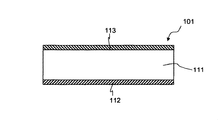
- FIG. 1 is a perspective view showing a configuration of a semiconductor radiation detector according to an embodiment of the present invention
- FIG. 2 is a cross-sectional view.
- a semiconductor radiation detector (hereinafter, simply referred to as “detector”) 101 is disposed on one semiconductor crystal 111 formed in a flat plate shape and one surface (lower surface) of the semiconductor crystal 111.
- the first electrode 112 and the second electrode 113 disposed on the other surface (upper surface) are provided.
- the semiconductor crystal 111 forms a region that generates electric charges by interacting with radiation ( ⁇ rays or the like), and is formed by cutting from a single crystal of thallium bromide.
- the thallium bromide single crystal is grown by a single crystal growth apparatus after purifying a 99.99% pure thallium bromide raw material.
- a commercially available 99.99% pure thallium bromide material contains lead (Pb) as an impurity.
- Examples of the purification treatment method include a zone refining method and a vacuum distillation method. In this example, the purification process was performed with the aim of reducing the lead concentration as an impurity in the crystal.
- the vertical Bridgman method is used as a single crystal growth method.
- the diameter of the crystal is about 3 inches.
- the degree of fluctuation of the crystal lattice of the grown crystal depends on the temperature gradient during growth, the growth rate, the shape of the crucible, the thermal conductivity of the crucible, etc.
- a single crystal ingot was grown to suppress fluctuations in the crystal lattice.
- a single crystal ingot of a comparative example was also grown by a growth process not paying attention to the degree of fluctuation of the crystal lattice.
- the single crystal ingot no. 1 and the comparative single crystal ingot No. Two two 3-inch single crystal ingots were obtained.
- the single crystal ingot is cut by an inner slicer parallel to the crystal growth surface when the ingot is grown, and then polished to obtain a 3-inch thallium bromide single crystal wafer having a thickness of 0.5 mm.
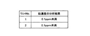
- FIG. 3 is an explanatory diagram of the concentration of lead as an impurity of a semiconductor crystal used in the semiconductor radiation detector according to one embodiment of the present invention and the semiconductor radiation detector of the comparative example.
- single crystal wafer No. 1 obtained from two types of 3 inch single crystal ingots. 1 and no. 2 shows a result of performing glow discharge mass spectrometry (GDMS: Glow Discharge Mass Spectrometry) in order to examine the concentration of lead as an impurity contained in 2.
- the detection limit of lead concentration by GDMS is 0.1 ppm. 1 and no. In both cases, lead is not detected, and both lead concentrations are less than 0.1 ppm.
- the single crystal wafer is diced to a size of 5.5 mm ⁇ 5.0 mm, for example, so that the semiconductor crystal 111 of the flat plate of the present embodiment shown in FIGS. 1 and 2 and the flat plate of the comparative example A semiconductor crystal is obtained.
- the first electrode 112 and the second electrode 113 are formed using gold, platinum, or palladium, and the thickness thereof is, for example, 50 nm.
- the dimensions of the first electrode 112 and the second electrode 113 are, for example, 5.5 mm ⁇ 5.0 mm.
- the dimensions of the semiconductor crystal 111, the first electrode 112, and the second electrode 113 described above are merely examples, and are not limited to the above dimensions.
- the wafer no Using the semiconductor crystal 111 obtained by dicing 1, the detector 101 of this embodiment and the wafer No.
- the detector of a comparative example is obtained using the semiconductor crystal obtained by dicing 2.
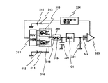
- FIG. 4 is a circuit diagram showing a circuit configuration when radiation measurement is performed using the semiconductor radiation detector according to one embodiment of the present invention.
- a smoothing capacitor 320 that applies a voltage to the detector 101, a first DC power supply 311 that supplies a positive charge to one electrode of the smoothing capacitor 320, and a negative charge to the one electrode of the smoothing capacitor 320.
- a second DC power supply 312 to be supplied is connected to the detector 101.
- first constant current diode 318 having a constant current characteristic polarity so that current flows from the first DC power supply 311 to the one electrode of the smoothing capacitor 320, and the one electrode of the smoothing capacitor 320 from the one electrode.
- a second constant current diode 319 having a constant current characteristic polarity so as to pass current to the second DC power supply 312 is connected between the first DC power supply 311 and the second DC power supply 312 and the detector 101. Has been.
- a first photoMOS relay 315 is connected between the first DC power supply 311 and the one electrode of the smoothing capacitor 320, and the second DC power supply 312 and the one electrode of the smoothing capacitor 320 are connected to each other.
- a second photo MOS relay 316 is connected between them.
- a protective resistor 313 is connected between the first DC power supply 311 and the first photoMOS relay 315, and a protective resistor is connected between the second DC power supply 312 and the second photomoss relay 316. 314 is connected.
- the protective resistors 313 and 314 are resistors for preventing overcurrent.
- the opening / closing of the first photoMOS relay 315 and the second photomoss relay 316 is controlled by the switch control device 317.
- one electrode of the bleeder resistor 321 and the coupling capacitor 322 is connected to the output of the detector 101, and an amplifier 323 that amplifies the signal of the detector 101 is connected to the other electrode of the coupling capacitor 322.
- the switch control device 317 and the amplifier 323 are connected to a polarity integrated control device 324 that controls the timing of opening / closing the photo MOS relays 315 and 316 and the polarity inversion of the amplifier 323.
- the negative pole of the first DC power supply 311, the positive pole of the second DC power supply 312, the other pole other than the one electrode of the smoothing capacitor 320, and one pole of the bleeder resistor 321 are each connected to the ground line.
- the first constant current diode 318 and the second constant current diode 319 are connected in series with the polarities of the constant current characteristics reversed to constitute a constant current device 361.
- the current general constant current diode used for the first constant current diode 318 and the second constant current diode 319 includes a source electrode and a gate electrode of a field effect transistor (FET). Since a constant current characteristic is created with a short-circuited structure, when a reverse voltage is applied, the pn junction formed in the field effect transistor is biased in the forward direction and a large current flows. That is, the current characteristic of the constant current diode has polarity. Therefore, the first constant current diode 318 and the second constant current diode 319 are connected in series with the polarities of the constant current characteristics reversed, so that constant current characteristics with no difference in polarity can be obtained.
- the first DC power source 311 or the second DC power source 312 and the smoothing capacitor 320 are used to collect charges between the first electrode 112 and the second electrode 113 of the detector 101.
- a bias voltage is applied (for example, + 500V or -500V).
- the semiconductor crystal 111 that is a member of the detector 101 is made of thallium bromide, when a bias voltage of, for example, +500 V is continuously applied to the detector 101 using the first DC power supply 311, Degradation of radiation measurement performance due to polarization, that is, charge bias, occurs in the semiconductor crystal 111, and the energy resolution of ⁇ rays deteriorates.
- the inversion period is, for example, 5 minutes.
- the switch control device 317 closes the first photoMOS relay 315 and opens the second photomoss relay 316 when a positive bias voltage is applied to the detector 101.
- the smoothing capacitor 320 is charged via the constant current device 361, and the voltage of the smoothing capacitor 320 becomes + 500V. Accordingly, the bias voltage applied to the detector 101 is also + 500V. Conversely, when a bias voltage of ⁇ 500 V is applied to the detector 101, a negative DC bias voltage is supplied by the second DC power supply 312.
- the switch control device 317 opens the first photo MOS relay 315 and closes the second photo MOS relay 316 when a negative bias voltage is applied to the detector 101.
- the smoothing capacitor 320 is charged via the constant current device 361, and the voltage of the smoothing capacitor 320 becomes ⁇ 500V. By accumulating positive charges or negative charges on one electrode of the smoothing capacitor 320, the bias voltage applied to the detector 101 is inverted between positive and negative.
- the polarity integrated control device 324 Based on the time information of polarity reversal every 5 minutes, the polarity integrated control device 324 sends “positive bias”, “negative bias”, “bias reversal from positive to negative”, “from negative to positive” to the switch control device 317 and the amplifier 323. A command signal of “bias reversal to positive” is transmitted.
- the switch control device 317 opens and closes the photo MOS relays 315 and 316 based on the command signal.
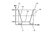
- FIG. 5 is an explanatory diagram of the time change of the bias voltage applied to the semiconductor radiation detector according to the embodiment of the present invention.
- the bias voltage applied to the detector 101 is initially the voltage V1 (+500 V), but changes to the voltage V3 ( ⁇ 500 V) due to the periodic inversion of the bias voltage, and again after 5 minutes, the voltage V5 Return to (+ 500V).
- the temporal changes in the voltages V2 and V4 along the way become a linear gradient. This is an effect of the constant current device 361. Further, while the bias voltage is inverted, the absolute value of the bias voltage is insufficient for charge collection and the ⁇ -ray detection signal cannot be sufficiently extracted, but the measurement interruption time (time t1, t2 during which the voltages V2, V4 are applied) ) Each is 0.3 seconds. A break time of 0.3 seconds occurs during the 5-minute measurement. However, when applying the semiconductor radiation detector to a nuclear medicine diagnostic device or homeland security, it is a sufficiently short time and does not cause a problem. .
- the generated charge is output from the detector 101 as a ⁇ -ray detection signal.
- This ⁇ -ray detection signal is input to the amplifier 323 via the coupling capacitor 322.
- the bleeder resistor 321 functions to prevent the charge from continuing to accumulate in the coupling capacitor 322 and to prevent the output voltage of the detector 101 from rising excessively.
- the amplifier 323 functions to convert and amplify a ⁇ -ray detection signal, which is a minute charge, into a voltage.
- the ⁇ -ray detection signal amplified by the amplifier 323 is converted into a digital signal by an analog / digital converter (not shown) at the subsequent stage, and counted by a data processing device (not shown) for each ⁇ -ray energy.
- FIGS. 6 and 7 are explanatory diagrams of a ⁇ -ray energy spectrum measured using the semiconductor radiation detector according to the embodiment of the present invention, respectively, and a ⁇ -ray energy spectrum measured using the semiconductor radiation detector of the comparative example. It is explanatory drawing.
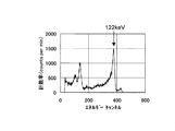
- FIG. 6 shows the wafer No. described above. The measurement result when the detector 101 is produced using the semiconductor crystal 111 cut out from 1 is shown.
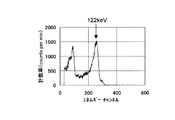
- 7 shows the wafer No. described above. The measurement result at the time of producing a detector using the semiconductor crystal cut out from 2 is shown.
- the horizontal axis indicates the channel number of the energy channel.
- Various energy gamma rays are assigned to each energy channel in association with each energy channel. For example, in FIG. 6, approximately 122 keV of ⁇ -ray energy is assigned to energy channels in the vicinity of approximately 380 channels.
- the vertical axis indicates the ⁇ -ray count rate (counts per min, counts per minute) of each energy channel.
- Energy resolution (%) (number of channels with half-width of peak) / (number of channels immediately under peak) ⁇ 100 (Equation 1)
- the energy resolution of 122 keV is about 5%
- the energy resolution of 122 keV is about 15%.
- the concentration of lead as an impurity of the semiconductor crystal less than 0.1 ppm, it is possible to measure the 122 keV ⁇ -ray energy spectrum for both the detector 101 of this embodiment and the detector of the comparative example. become.
- there is a large difference in energy resolution between the semiconductor radiation detector of the present embodiment and the comparative example and 8% or less can be realized in the detector 101 of the present embodiment, whereas in the detector of the comparative example. Is worse than 8%.
- the present invention has been made based on the new knowledge of the present inventor that the energy resolution of the semiconductor radiation detector depends on the X-ray diffraction rocking curve of the semiconductor crystal.
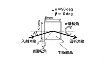
- FIG. 8 is an explanatory diagram of the sample arrangement in the X-ray diffraction rocking curve measurement of the semiconductor crystal 111.
- X-rays are made incident on the sample crystal (TlBr crystal) and diffracted X-rays are detected, but the detection angle of the diffracted X-rays is fixed, and the sample tilt angle ⁇ and rotation angle
- Three diffraction intensity profiles are acquired by changing the incident angle ⁇ of incident X-rays.
- the full width at half maximum of the diffraction intensity peak is defined as ⁇ rocking curve half width, ⁇ rocking curve half width, and ⁇ rocking curve half width.
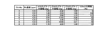
- FIG. 9 is an explanatory diagram of the lead concentration, the X-ray diffraction rocking curve half width, and the energy resolution of the semiconductor crystal 111 of this embodiment and the semiconductor crystal of the comparative example.
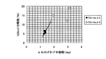
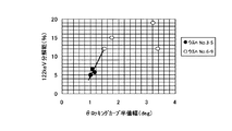
- 10 to 12 show the sample inclination angle ( ⁇ ) rocking curve half-value width and sample in-plane rotation angle ( ⁇ ) rocking curve of the semiconductor crystal used in the detector 101 according to the present embodiment and the detector of the comparative example, respectively.
- It is explanatory drawing which shows the relationship between the half value width, X-ray incident angle ((theta)) rocking curve half value width, and the 122 keV energy resolution of the detector 101 and the detector of a comparative example.
- Three wafers used as the semiconductor crystal 111 of this embodiment namely No. 3 to 5 and four wafers used as semiconductor crystals of comparative examples,
- the lead concentration, the degree of fluctuation of the crystal lattice, that is, the half value width of the X-ray diffraction rocking curve, and the 122 keV energy resolution were evaluated for 6 to 9 wafers in total.
- the seven wafer raw materials were subjected to a purification process aiming to reduce the lead concentration as impurities in the crystal, and the lead concentration of all the seven wafers by GDMS was less than 0.1 ppm.
- the ⁇ rocking curve half width in the sample tilt angle scan is 1.6 deg or less
- the ⁇ rocking curve half width in the sample in-plane rotation angle scan is 3.5 deg or less
- the ⁇ rocking curve half width in the X-ray incident angle scan is 1.
- Three measurement points that are 3 degrees or less are the wafer numbers of this embodiment. 3 to 5 and the other four measurement points are the wafer numbers of comparative examples.
- the lead concentration is less than 0.1 ppm
- the ⁇ rocking curve half width is 1.6 deg or less
- the ⁇ rocking curve half width is 3.5 deg or less
- the ⁇ rocking curve half width is 1.3 deg or less
- a 122 keV energy resolution of 8% or less can be obtained.
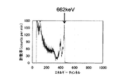
- FIG. 13 shows the ingot No. described above. No. 1 obtained from wafer No. 1
- the measurement result when the detector 101 is produced using the semiconductor crystal 111 cut out from 1 is shown.
- the horizontal axis indicates the channel number of the energy channel.
- the vertical axis represents the gamma ray count rate (counts per min, counts per minute) of each energy channel.
- the detector 101 of this embodiment shown in FIG. By using the semiconductor crystal 111 cut out from 1, an energy spectrum of 662 keV can be obtained with high energy resolution.
- the detector 101 of this embodiment is 122 keV and 662 keV in terms of radiation measurement performance, compared to the case where the detector is configured using the conventional thallium bromide crystal described in Non-Patent Document 1 as a semiconductor crystal.
- the energy resolution of 8% or less can be obtained at 122 keV, and a high energy resolution can be obtained even at 662 keV.
- the semiconductor crystal 111 has a lead concentration of less than 0.1 ppm and a full width at half maximum in the sample tilt angle scan of the (110) rocking curve in X-ray diffraction is 1.
- the concentration of lead atoms in the thallium bromide single crystal is small, so that lead atoms are substituted for thallium atoms.
- the density of defects in the resulting crystal is reduced and the charge carrier capture length can be increased, so that 122 gV and 662 keV ⁇ -ray energy spectra can be measured as a radiation detector.
- a single crystal of thallium bromide having a lead concentration of less than 0.1 ppm is used as the semiconductor crystal, which means that the lead concentration is limited to the detection limit of lead in glow discharge mass spectrometry (GDMS: Glow Discharge Mass Mass Spectrometry). It can also be said that the following single crystal of thallium bromide is used.
- GDMS glow discharge mass spectrometry
- using a thallium bromide single crystal having a lead concentration of less than 0.1 ppm as a semiconductor crystal means using a thallium bromide single crystal having a lead concentration of 0.0 ppm as the semiconductor crystal.
- the lead concentration of 0.0 ppm means that the number of digits with two or less significant digits is not limited, for example, lead of 0.099 ppm, 0.09 ppm, 0.04 ppm, or 0.01 ppm or less. Includes concentration.
- a single crystal of thallium bromide with a lead concentration of less than 0.1 ppm means that a single crystal of thallium bromide that does not contain a lead substitutional solid solution is used as the semiconductor crystal. You can also. This is because, when the lead concentration is as low as less than 0.1 ppm, some of the thallium atoms are not substituted by the lead impurity, so that a substitutional solid solution is not formed and defects are not generated, so that charge carriers are captured. Difficult to capture long. Therefore, by using such a semiconductor crystal, 122 keV and 662 keV ⁇ -ray energy spectra can be measured as a radiation detector.
- the use of a single crystal of thallium bromide having a lead concentration of less than 0.1 ppm as the semiconductor crystal means that a single crystal of thallium bromide having no defects in which charge carriers are trapped is used as the semiconductor crystal. You can also. This is because when the lead concentration is as low as less than 0.1 ppm, a part of the thallium atom is not substituted by the lead impurity, so that a substitutional solid solution is not formed, and defects that trap charge carriers do not occur. Charge carriers are not easily captured and the capture length is increased. Therefore, by using such a semiconductor crystal, 122 keV and 662 keV ⁇ -ray energy spectra can be measured as a radiation detector.
- the full width at half maximum in the sample tilt angle scan of the (110) rocking curve in X-ray diffraction is 1.6 degs or less
- the full width at half maximum in the in-plane rotation angle scan is 3.5 degs or less
- the X-ray incident angle scan By using a single crystal of thallium bromide having a full width at half maximum of 1.3 deg or less, fluctuations of the crystal lattice in the single crystal can be reduced, so that the product of charge carrier mobility and lifetime can be increased.
- a radiation detector a 122 keV ⁇ -ray energy spectrum can be measured with a higher energy resolution, that is, an energy resolution of 8% or less.
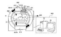
- FIGS. 14 and 15 are configuration diagrams of a nuclear medicine diagnostic apparatus using a semiconductor radiation detector according to an embodiment of the present invention.
- a SPECT imaging apparatus 600 includes two radiation detection blocks 601A and 601B positioned above and below, a rotation support base 606, a bed 31 so as to surround a cylindrical measurement region 602 in the center portion.
- An image information creation device 603 is provided.
- the radiation detection block 601A located on the upper side includes a plurality of radiation measurement units 611, a unit support member 615, and a light shielding / electromagnetic shield 613.
- the radiation measurement unit 611 includes a plurality of semiconductor radiation detectors 101, a substrate 612, and a collimator 614.
- the radiation detection block 601B located at the lower part has the same configuration.
- the image information creation device 603 includes a data processing device 32 and a display device 33.
- the radiation detection blocks 601A and 601B are arranged at positions shifted by 180 degrees in the circumferential direction on the rotation support base 606. Specifically, each unit support member 615 (only one is shown) of each of the radiation detection blocks 601A and 601B is attached to the rotation support base 606 at a position 180 degrees apart in the circumferential direction. A plurality of radiation measurement units 611 including the substrate 612 are detachably attached to the unit support member 615.
- the plurality of detectors 101 are arranged in multiple stages in a state of being attached to the substrate 612 in the region K partitioned by the collimator 614.
- the collimator 614 is formed of a radiation shielding material (for example, lead, tungsten, etc.), and forms a large number of radiation paths through which radiation (for example, ⁇ rays) passes.
- All the substrates 612 and the collimators 614 are arranged in a light shielding / electromagnetic shield 613 installed on the rotation support base 606.
- the light shielding / electromagnetic shield 613 blocks the influence of electromagnetic waves other than ⁇ rays on the detector 101 and the like.
- the emitted ⁇ -rays When ⁇ -rays are emitted from the accumulation part (for example, affected part) D in the subject H where the radiopharmaceutical is accumulated, the emitted ⁇ -rays enter the corresponding detector 101 through the radiation path of the collimator 614. To do.
- the detector 101 outputs a ⁇ -ray detection signal.
- the ⁇ -ray detection signal is counted by the data processing device 32 for each ⁇ -ray energy, and the information is displayed on the display device 33.
- the radiation detection blocks 601A and 601B rotate as indicated by thick arrows while being supported by the rotation support base 606, and perform imaging and measurement while changing the angle with the subject H. Further, the radiation detection blocks 601A and 601B are movable up and down as indicated by thin arrows, and the distance from the subject H can be changed.
- the detector 101 used in such a SPECT imaging apparatus 600 can measure a 122 keV ⁇ -ray energy spectrum with a high energy resolution of 8% or less while using thallium bromide as a semiconductor crystal. Therefore, 99m Tc that emits 141 keV gamma rays and 123 I that emits 159 keV gamma rays, which are typical radionuclides used for radiopharmaceuticals for nuclear medicine examinations, are small in size and high in energy resolution. It is possible to provide a SPECT imaging apparatus capable of simultaneous radionuclide imaging.
- the detector 101 is not limited to the SPECT imaging apparatus 600 but can be used for a gamma camera apparatus, a PET imaging apparatus, or the like as a nuclear medicine diagnostic apparatus.
- a positron emission tomographic imaging apparatus (PET imaging apparatus) 700 includes an imaging apparatus 701 having a cylindrical measurement region 702 at the center, and a bed 31 that supports a subject H and is movable in the longitudinal direction.
- the image information creating apparatus 703 is provided.
- the image information creation device 703 includes a data processing device 32 and a display device 33.
- a substrate P on which a large number of the detectors 101 are mounted is disposed so as to surround the measurement region 702.
- Such a PET imaging apparatus 700 includes a digital ASIC having a data processing function (Application Specific Integrated Circuit for digital circuit, application-specific integrated circuit for digital circuit, not shown) and the like, A packet having the time and the detection channel ID (Identification) of the detector 101 is created, and the created packet is input to the data processing device 32.
- a digital ASIC having a data processing function (Application Specific Integrated Circuit for digital circuit, application-specific integrated circuit for digital circuit, not shown) and the like
- a packet having the time and the detection channel ID (Identification) of the detector 101 is created, and the created packet is input to the data processing device 32.
- the detector 101 detects ⁇ rays emitted from the body of the subject H due to the radiopharmaceutical. That is, when the positrons emitted from the radiopharmaceutical for PET imaging are extinguished, a pair of ⁇ rays are emitted in opposite directions of about 180 degrees, and are detected by separate detection channels among the many detectors 101.
- the detected ⁇ -ray detection signal is input to the corresponding digital ASIC, signal processing is performed as described above, and the position information of the detection channel that detected the ⁇ -ray and the detection time information of the ⁇ -ray are processed by data processing. Input to the device 32.
- the data processing device 32 counts (simultaneously counts) a pair of ⁇ -rays generated by the disappearance of one positron as one, and determines the positions of the two detection channels that detected the pair of ⁇ -rays as their positions. Identify based on information.
- the data processing device 32 creates tomographic image information (image information) of the subject H at the radiopharmaceutical accumulation position, that is, the tumor position, using the count value obtained by the coincidence counting and the position information of the detection channel. . This tomographic image information is displayed on the display device 33.
- the detector 101 used in such a PET imaging apparatus 700 can measure a 662 keV ⁇ -ray energy spectrum with high energy resolution while using thallium bromide as a semiconductor crystal. Therefore, it is possible to provide a PET imaging apparatus that is small and inexpensive and can detect 511 keV ⁇ rays emitted from positrons generated from a radiopharmaceutical for PET examination with high energy resolution.
- the present embodiment while using thallium bromide as a semiconductor crystal constituting the radiation detector, it is possible to measure 122 keV and 662 keV ⁇ -ray energy spectra with high energy resolution by the radiation detector. is there. Therefore, it is possible to provide a semiconductor radiation detector that is small, inexpensive, and has high energy resolution, and a nuclear medicine diagnostic apparatus equipped with this semiconductor radiation detector.
- the semiconductor radiation detector of the present invention and the nuclear medicine diagnostic apparatus equipped with the semiconductor radiation detector are capable of imaging radiopharmaceuticals with high energy resolution, and can be downsized and reduced in price. Widely used and adopted in this field.
- SPECT imaging device 601A, 601B Radiation detection blocks 602, 702 ... Measurement areas 603, 703 ... Image information creation device 606 ; Rotation support base 611 . Radiation measurement unit 612 ... Substrate 613 ... Light shielding / electromagnetic shield 614 ... Collimator 615 ... Unit support member 700 ... PET imaging Device 701 ... Imaging device D ... Stacking unit ... areas P ... substrate partitioned by the subject K ... collimator
Landscapes
- Health & Medical Sciences (AREA)
- Life Sciences & Earth Sciences (AREA)
- Engineering & Computer Science (AREA)
- Medical Informatics (AREA)
- Physics & Mathematics (AREA)
- Molecular Biology (AREA)
- High Energy & Nuclear Physics (AREA)
- Heart & Thoracic Surgery (AREA)
- General Health & Medical Sciences (AREA)
- Pathology (AREA)
- Radiology & Medical Imaging (AREA)
- Biomedical Technology (AREA)
- Nuclear Medicine, Radiotherapy & Molecular Imaging (AREA)
- Biophysics (AREA)
- Surgery (AREA)
- Animal Behavior & Ethology (AREA)
- Optics & Photonics (AREA)
- Public Health (AREA)
- Veterinary Medicine (AREA)
- General Physics & Mathematics (AREA)
- Spectroscopy & Molecular Physics (AREA)
- Measurement Of Radiation (AREA)
- Nuclear Medicine (AREA)
- Light Receiving Elements (AREA)
- Manufacturing & Machinery (AREA)
Priority Applications (3)
| Application Number | Priority Date | Filing Date | Title |
|---|---|---|---|
| CN201480052242.3A CN105579868A (zh) | 2013-10-03 | 2014-09-30 | 半导体放射线检测器、使用其的核医学诊断装置、以及半导体放射线检测器的制造方法 |
| US15/025,580 US20160206257A1 (en) | 2013-10-03 | 2014-09-30 | Semiconductor radiation detector, nuclear medicine diagnostic device using that detector, and manufacturing method of semiconductor radiation detector |
| EP14851321.1A EP3054321A4 (en) | 2013-10-03 | 2014-09-30 | Semiconductor radiation detector, nuclear medicine diagnostic device using same, and method for producing semiconductor radiation detector |
Applications Claiming Priority (2)
| Application Number | Priority Date | Filing Date | Title |
|---|---|---|---|
| JP2013208107A JP2015072201A (ja) | 2013-10-03 | 2013-10-03 | 半導体放射線検出器、それを用いた核医学診断装置、および半導体放射線検出器の製造方法 |
| JP2013-208107 | 2013-10-03 |
Publications (1)
| Publication Number | Publication Date |
|---|---|
| WO2015050141A1 true WO2015050141A1 (ja) | 2015-04-09 |
Family
ID=52778729
Family Applications (1)
| Application Number | Title | Priority Date | Filing Date |
|---|---|---|---|
| PCT/JP2014/076195 Ceased WO2015050141A1 (ja) | 2013-10-03 | 2014-09-30 | 半導体放射線検出器、それを用いた核医学診断装置、および半導体放射線検出器の製造方法 |
Country Status (5)
| Country | Link |
|---|---|
| US (1) | US20160206257A1 (enExample) |
| EP (1) | EP3054321A4 (enExample) |
| JP (1) | JP2015072201A (enExample) |
| CN (1) | CN105579868A (enExample) |
| WO (1) | WO2015050141A1 (enExample) |
Cited By (2)
| Publication number | Priority date | Publication date | Assignee | Title |
|---|---|---|---|---|
| CN105759304A (zh) * | 2016-04-22 | 2016-07-13 | 西北核技术研究所 | 一种基于平晶衍射成像的x射线能谱测量方法 |
| CN108345026A (zh) * | 2018-02-09 | 2018-07-31 | 哈尔滨工业大学 | 一种计算带电粒子防护层后能谱的方法 |
Families Citing this family (6)
| Publication number | Priority date | Publication date | Assignee | Title |
|---|---|---|---|---|
| JP6242954B1 (ja) | 2016-07-11 | 2017-12-06 | 浜松ホトニクス株式会社 | 放射線検出器 |
| EP3704515B1 (en) * | 2017-10-30 | 2022-04-06 | Shenzhen Xpectvision Technology Co., Ltd. | Radiation detector with dc-to-dc converter based on mems switches |
| CN108763758B (zh) * | 2018-05-29 | 2022-05-03 | 南京航空航天大学 | 一种非完备环状pet旋转扫描模式的gate仿真方法 |
| JP6970801B2 (ja) * | 2018-10-31 | 2021-11-24 | 浜松ホトニクス株式会社 | 放射線検出器製造方法 |
| JP6688861B1 (ja) * | 2018-11-12 | 2020-04-28 | 浜松ホトニクス株式会社 | 放射線検出器及びその製造方法 |
| JP7051928B2 (ja) * | 2020-04-06 | 2022-04-11 | 浜松ホトニクス株式会社 | 放射線検出器の製造方法 |
Citations (4)
| Publication number | Priority date | Publication date | Assignee | Title |
|---|---|---|---|---|
| JP2001349948A (ja) * | 2000-06-08 | 2001-12-21 | Nec Corp | X線発光素子 |
| JP2005223009A (ja) * | 2004-02-03 | 2005-08-18 | Hitachi Ltd | 半導体放射線検出器及び放射線検出装置 |
| JP2009286856A (ja) * | 2008-05-27 | 2009-12-10 | Fukuda Crystal Laboratory | シンチレータ材料とその製造方法、及び、電離放射線検出器 |
| JP2013156048A (ja) * | 2012-01-27 | 2013-08-15 | Hitachi Ltd | 半導体放射線検出器および核医学診断装置 |
Family Cites Families (7)
| Publication number | Priority date | Publication date | Assignee | Title |
|---|---|---|---|---|
| JP3863873B2 (ja) * | 2003-09-30 | 2006-12-27 | 株式会社日立製作所 | 放射線検査装置 |
| JPWO2009022378A1 (ja) * | 2007-08-10 | 2010-11-11 | 学校法人 大阪電気通信大学 | 放射線検出装置 |
| WO2011010724A1 (ja) * | 2009-07-23 | 2011-01-27 | 住友電気工業株式会社 | 半導体結晶の製造方法、半導体結晶の製造装置および半導体結晶 |
| JP4902759B2 (ja) * | 2010-03-10 | 2012-03-21 | 株式会社日立製作所 | 放射線計測装置および核医学診断装置 |
| DE112011101561T8 (de) * | 2010-05-03 | 2013-04-18 | Brookhaven Science Associates Llc | Array von virtuellen Frisch-Gitter-Detektoren mit gemeinsamer Kathode und reduzierter Länge der Schirmelektroden |
| JP5485197B2 (ja) * | 2011-02-10 | 2014-05-07 | 株式会社日立製作所 | 放射線計測装置および核医学診断装置 |
| JP6120041B2 (ja) * | 2012-01-31 | 2017-04-26 | Jx金属株式会社 | 放射線検出素子および放射線検出器 |
-
2013
- 2013-10-03 JP JP2013208107A patent/JP2015072201A/ja active Pending
-
2014
- 2014-09-30 EP EP14851321.1A patent/EP3054321A4/en not_active Withdrawn
- 2014-09-30 US US15/025,580 patent/US20160206257A1/en not_active Abandoned
- 2014-09-30 CN CN201480052242.3A patent/CN105579868A/zh active Pending
- 2014-09-30 WO PCT/JP2014/076195 patent/WO2015050141A1/ja not_active Ceased
Patent Citations (4)
| Publication number | Priority date | Publication date | Assignee | Title |
|---|---|---|---|---|
| JP2001349948A (ja) * | 2000-06-08 | 2001-12-21 | Nec Corp | X線発光素子 |
| JP2005223009A (ja) * | 2004-02-03 | 2005-08-18 | Hitachi Ltd | 半導体放射線検出器及び放射線検出装置 |
| JP2009286856A (ja) * | 2008-05-27 | 2009-12-10 | Fukuda Crystal Laboratory | シンチレータ材料とその製造方法、及び、電離放射線検出器 |
| JP2013156048A (ja) * | 2012-01-27 | 2013-08-15 | Hitachi Ltd | 半導体放射線検出器および核医学診断装置 |
Non-Patent Citations (4)
| Title |
|---|
| "Chemical Handbook Fundamentals" |
| NUCLEAR INSTRUMENTS AND METHODS IN PHYSICS RESEARCH SECTION-A, vol. 591, 2008, pages 209 - 212 |
| NUCLEAR INSTRUMENTS AND METHODS IN PHYSICS RESEARCH SECTION-A, vol. 633, 2011, pages 572 - 574 |
| See also references of EP3054321A4 |
Cited By (3)
| Publication number | Priority date | Publication date | Assignee | Title |
|---|---|---|---|---|
| CN105759304A (zh) * | 2016-04-22 | 2016-07-13 | 西北核技术研究所 | 一种基于平晶衍射成像的x射线能谱测量方法 |
| CN108345026A (zh) * | 2018-02-09 | 2018-07-31 | 哈尔滨工业大学 | 一种计算带电粒子防护层后能谱的方法 |
| CN108345026B (zh) * | 2018-02-09 | 2021-06-15 | 哈尔滨工业大学 | 一种计算带电粒子防护层后能谱的方法 |
Also Published As
| Publication number | Publication date |
|---|---|
| EP3054321A1 (en) | 2016-08-10 |
| EP3054321A4 (en) | 2017-05-31 |
| CN105579868A (zh) | 2016-05-11 |
| JP2015072201A (ja) | 2015-04-16 |
| US20160206257A1 (en) | 2016-07-21 |
Similar Documents
| Publication | Publication Date | Title |
|---|---|---|
| WO2015050141A1 (ja) | 半導体放射線検出器、それを用いた核医学診断装置、および半導体放射線検出器の製造方法 | |
| JP6049166B2 (ja) | 半導体放射線検出器およびそれを用いた核医学診断装置 | |
| Hou et al. | Materials innovation and electrical engineering in X-ray detection | |
| US8816292B2 (en) | Compact endocavity diagnostic probes for nuclear radiation detection | |
| Churilov et al. | Thallium bromide nuclear radiation detector development | |
| Gokhale et al. | Growth, fabrication, and testing of bismuth tri-iodide semiconductor radiation detectors | |
| JP5753802B2 (ja) | 半導体放射線検出器および核医学診断装置 | |
| Hitomi et al. | TlBr capacitive Frisch grid detectors | |
| Chaudhuri et al. | Quaternary semiconductor Cd1− xZnxTe1− ySey for high-resolution, room-temperature gamma-ray detection | |
| Onodera et al. | Pixellated thallium bromide detectors for gamma-ray spectroscopy and imaging | |
| CN107148582A (zh) | 用于具有改进的内部电场的检测器的系统和方法 | |
| Hitomi et al. | Recent development of TlBr gamma-ray detectors | |
| Onodera et al. | Spectroscopic performance of pixellated thallium bromide detectors | |
| JP5485197B2 (ja) | 放射線計測装置および核医学診断装置 | |
| Hitomi et al. | TlBr gamma-ray spectrometers using the depth sensitive single polarity charge sensing technique | |
| Hitomi et al. | Timing performance of TlBr detectors | |
| EP3073291A1 (en) | Radiation detection element, radiation detector provided with same, nuclear medicine diagnosis device and method for producing radiation detection element | |
| Li et al. | A new method for growing detector-grade cadmium zinc telluride crystals | |
| Hitomi et al. | Large-volume thallium bromide detectors for gamma-ray spectroscopy | |
| Hitomi et al. | Thallium lead iodide radiation detectors | |
| Roos | Semiconductor Detectors | |
| Onodera et al. | Temperature dependence of spectroscopic performance of thallium bromide X-and gamma-ray detectors | |
| WO2016088640A1 (ja) | 半導体結晶の製造方法、半導体放射線検出器、およびそれを用いた放射線撮像装置 | |
| Kim et al. | Thallium bromide and thallium bromoiodide gamma ray spectrometer development | |
| Oliveira et al. | Gamma-ray spectroscopy for TlBr detectors at two different temperatures |
Legal Events
| Date | Code | Title | Description |
|---|---|---|---|
| WWE | Wipo information: entry into national phase |
Ref document number: 201480052242.3 Country of ref document: CN |
|
| 121 | Ep: the epo has been informed by wipo that ep was designated in this application |
Ref document number: 14851321 Country of ref document: EP Kind code of ref document: A1 |
|
| REEP | Request for entry into the european phase |
Ref document number: 2014851321 Country of ref document: EP |
|
| WWE | Wipo information: entry into national phase |
Ref document number: 2014851321 Country of ref document: EP |
|
| WWE | Wipo information: entry into national phase |
Ref document number: 15025580 Country of ref document: US |
|
| NENP | Non-entry into the national phase |
Ref country code: DE |