WO2015049983A1 - 光電変換装置および光電変換装置の製造方法 - Google Patents
光電変換装置および光電変換装置の製造方法 Download PDFInfo
- Publication number
- WO2015049983A1 WO2015049983A1 PCT/JP2014/074497 JP2014074497W WO2015049983A1 WO 2015049983 A1 WO2015049983 A1 WO 2015049983A1 JP 2014074497 W JP2014074497 W JP 2014074497W WO 2015049983 A1 WO2015049983 A1 WO 2015049983A1
- Authority
- WO
- WIPO (PCT)
- Prior art keywords
- photoelectric conversion
- layer
- conductive layer
- conversion module
- substrate
- Prior art date
- Legal status (The legal status is an assumption and is not a legal conclusion. Google has not performed a legal analysis and makes no representation as to the accuracy of the status listed.)
- Ceased
Links
Images








Classifications
-
- H—ELECTRICITY
- H01—ELECTRIC ELEMENTS
- H01G—CAPACITORS; CAPACITORS, RECTIFIERS, DETECTORS, SWITCHING DEVICES, LIGHT-SENSITIVE OR TEMPERATURE-SENSITIVE DEVICES OF THE ELECTROLYTIC TYPE
- H01G9/00—Electrolytic capacitors, rectifiers, detectors, switching devices, light-sensitive or temperature-sensitive devices; Processes of their manufacture
- H01G9/20—Light-sensitive devices
- H01G9/209—Light trapping arrangements
-
- H—ELECTRICITY
- H01—ELECTRIC ELEMENTS
- H01G—CAPACITORS; CAPACITORS, RECTIFIERS, DETECTORS, SWITCHING DEVICES, LIGHT-SENSITIVE OR TEMPERATURE-SENSITIVE DEVICES OF THE ELECTROLYTIC TYPE
- H01G9/00—Electrolytic capacitors, rectifiers, detectors, switching devices, light-sensitive or temperature-sensitive devices; Processes of their manufacture
- H01G9/20—Light-sensitive devices
- H01G9/2068—Panels or arrays of photoelectrochemical cells, e.g. photovoltaic modules based on photoelectrochemical cells
- H01G9/2081—Serial interconnection of cells
-
- Y—GENERAL TAGGING OF NEW TECHNOLOGICAL DEVELOPMENTS; GENERAL TAGGING OF CROSS-SECTIONAL TECHNOLOGIES SPANNING OVER SEVERAL SECTIONS OF THE IPC; TECHNICAL SUBJECTS COVERED BY FORMER USPC CROSS-REFERENCE ART COLLECTIONS [XRACs] AND DIGESTS
- Y02—TECHNOLOGIES OR APPLICATIONS FOR MITIGATION OR ADAPTATION AGAINST CLIMATE CHANGE
- Y02E—REDUCTION OF GREENHOUSE GAS [GHG] EMISSIONS, RELATED TO ENERGY GENERATION, TRANSMISSION OR DISTRIBUTION
- Y02E10/00—Energy generation through renewable energy sources
- Y02E10/50—Photovoltaic [PV] energy
- Y02E10/542—Dye sensitized solar cells
-
- Y—GENERAL TAGGING OF NEW TECHNOLOGICAL DEVELOPMENTS; GENERAL TAGGING OF CROSS-SECTIONAL TECHNOLOGIES SPANNING OVER SEVERAL SECTIONS OF THE IPC; TECHNICAL SUBJECTS COVERED BY FORMER USPC CROSS-REFERENCE ART COLLECTIONS [XRACs] AND DIGESTS
- Y02—TECHNOLOGIES OR APPLICATIONS FOR MITIGATION OR ADAPTATION AGAINST CLIMATE CHANGE
- Y02P—CLIMATE CHANGE MITIGATION TECHNOLOGIES IN THE PRODUCTION OR PROCESSING OF GOODS
- Y02P70/00—Climate change mitigation technologies in the production process for final industrial or consumer products
- Y02P70/50—Manufacturing or production processes characterised by the final manufactured product
Definitions
- the present invention relates to a photoelectric conversion device and a method for manufacturing the photoelectric conversion device.
- Patent Document 1 describes a photovoltaic cell using a chromophore coated on titanium oxide as a new type of solar cell.
- the photovoltaic cell described in Patent Document 1 has a structure in which a metal carrier, a metal oxide semiconductor layer made of titanium oxide, a monolayer of a sensitizer or a chromophore, an electrolyte layer, and an electrode are provided in this order between insulating layers. is doing.
- a redox-based 10 ⁇ 2 M solution containing 1 mM HClO 4 is used for the electrolyte layer of the photovoltaic cell described in Patent Document 1.
- Non-Patent Document 1 discloses a W-type series-connected dye-sensitized solar cell in which a plurality of dye-sensitized solar cells are connected in series.
- the module is M.M. Proposed by Somemeling et al.
- Patent Document 2 proposes a solar cell module in which dye-sensitized solar cells using nanoporous photoelectrodes on which a sensitizing dye is adsorbed are electrically connected in series.
- Non-Patent Document 1 and Patent Document 2 since the photoelectric conversion layer is porous, the amount of power generation is unlikely to decrease even when light does not enter the light-receiving surface perpendicularly. Electricity can be generated by scattered light reflected from surrounding objects. For this reason, it has been studied to install these solar cell modules on a surface having an angle close to the vertical such as a wall surface to produce a solar power generation device.
- the embodiment which is an example of the present invention is a photoelectric conversion device and a photoelectric conversion device capable of suppressing deterioration in characteristics even when installed so as to form an angle of 20 ° or more with respect to the horizontal. It aims at providing the manufacturing method of.
- the photoelectric conversion module includes a photoelectric conversion module in which two or more of the photoelectric conversion elements are electrically connected.
- the photoelectric conversion element includes: a substrate; a first conductive layer on the substrate; A photoelectric conversion layer on one conductive layer; a second conductive layer on the photoelectric conversion layer; and a charge transport layer on the first conductive layer, wherein the photoelectric conversion layer includes a porous semiconductor layer and a porous semiconductor layer.
- the charge transport layer contains an electrolyte, the photoelectric conversion module makes an angle of 20 ° or more with respect to the horizontal, and the positive side of the photoelectric conversion module is perpendicular to the negative side It is possible to provide a photoelectric conversion device that is installed so as to be higher.
- a conversion layer, a second conductive layer on the photoelectric conversion layer, and a charge transport layer on the first conductive layer, the photoelectric conversion layer comprising a porous semiconductor layer and a photosensitization adsorbed on the porous semiconductor layer And a charge transport layer can provide a method for manufacturing a photoelectric conversion device including an electrolytic solution.
- the photoelectric conversion device and a method for manufacturing the photoelectric conversion device that can suppress deterioration in characteristics even when installed so as to form an angle of 20 ° or more with respect to the horizontal. it can.
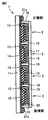
- FIG. 1 is a schematic perspective view of a photoelectric conversion device according to Embodiment 1.
- FIG. It is typical sectional drawing of an example of the photoelectric conversion module used for the photoelectric conversion apparatus of Embodiment 1.
- FIG. It is a typical side view of an example of the form in which the photoelectric conversion module is installed in the photoelectric conversion apparatus of Embodiment 1.
- 6 is a schematic cross-sectional view of a photoelectric conversion module according to Embodiment 2.
- FIG. 6 is a schematic enlarged cross-sectional view of a photoelectric conversion module according to Embodiment 3.
- FIG. 6 is a schematic enlarged cross-sectional view of a photoelectric conversion module according to Embodiment 4.
- FIG. 5 is a schematic cross-sectional view illustrating a part of the manufacturing process of the example of the method for manufacturing the photoelectric conversion module according to Embodiments 1 to 4.
- FIG. 5 is a schematic cross-sectional view illustrating a part of the manufacturing process of the example of the method for manufacturing the photoelectric conversion module according to Embodiments 1 to 4.
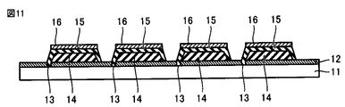
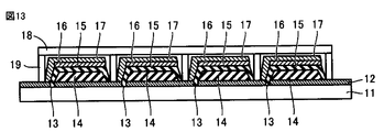
- FIG. 5 is a schematic cross-sectional view illustrating a part of the manufacturing process of the example of the method for manufacturing the photoelectric conversion module according to Embodiments 1 to 4.
- FIG. 5 is a schematic cross-sectional view illustrating a part of the manufacturing process of the example of the method for manufacturing the photoelectric conversion module according to Embodiments 1 to 4.
- FIG. 5 is a schematic cross-sectional view illustrating a part of the manufacturing process of the example of the method for manufacturing the photoelectric conversion module according to Embodiments 1 to 4.
- FIG. 5 is a schematic cross-sectional view illustrating a part of the manufacturing process of the example of the method for manufacturing the photoelectric conversion module according to Embodiments 1 to 4.
- FIG. 5 is a schematic cross-sectional view illustrating a part of the manufacturing process of the example of the method for manufacturing the photoelectric conversion module according to Embodiments 1 to 4.
- FIG. 5 is a schematic cross-sectional view illustrating a part of the manufacturing process of the example of the method for manufacturing the photoelectric conversion module according to Embodiments 1 to 4.
- FIG. 5 is a schematic cross-sectional view illustrating a part of the manufacturing process of the example of the method for manufacturing the photoelectric conversion module according to Embodiments 1 to 4.
- FIG. 1 the typical perspective view of the photoelectric conversion apparatus of Embodiment 1 is shown.
- the photoelectric conversion apparatus of Embodiment 1 includes a photoelectric conversion module 1, and the photoelectric conversion module 1 includes two or more photoelectric conversion elements 2 that are electrically connected.
- the photoelectric conversion module 1 has the four photoelectric conversion elements 2 electrically connected in series, but the number of the photoelectric conversion elements 2 is two or more. There is no particular limitation as long as it is present.
- the photoelectric conversion module 1 is installed on the installation surface 3, it is not limited to the structure shown in FIG.
- FIG. 2 shows a schematic cross-sectional view of an example of the photoelectric conversion module 1 used in the photoelectric conversion apparatus according to the first embodiment. Note that FIG. 2 corresponds to an example of a cross section taken along II-II of the photoelectric conversion device of Embodiment 1 of FIG.
- the four photoelectric conversion elements 2 constituting the photoelectric conversion module 1 of Embodiment 1 shown in FIG. 2 are respectively a substrate 11, a first conductive layer 12 on the substrate 11, and a photoelectric on the first conductive layer 12.
- current collecting electrodes 21 a and 21 b that are electrically connected to the first conductive layer 12 and collect current are provided at both ends in the connecting direction of the photoelectric conversion element 2 of the photoelectric conversion module 1.
- each photoelectric conversion element 2 since the first conductive layer 12 is a negative electrode and the second conductive layer 17 is a positive electrode, the current collection electrode 21a side of the photoelectric conversion module 1 is a positive electrode side, and the current collection electrode 21b side is a negative electrode. Become the side.
- the photoelectric conversion layer 14 of the photoelectric conversion element 2 includes a porous semiconductor layer and a photosensitizer adsorbed on the porous semiconductor layer. Further, the charge transport layer 20 contains an electrolytic solution, and the electrolytic solution contained in the charge transport layer 20 is photoelectrically converted through holes provided in the porous insulating layer 15, the catalyst layer 16, and the second conductive layer 17. The layer 14 penetrates into the porous semiconductor layer.
- Each photoelectric conversion element 2 is surrounded by the support 18 and the sealing portion 19. Adjacent photoelectric conversion elements 2 are connected in series by conduction through the first conductive layer 12, the photoelectric conversion layer 14, the porous insulating layer 15, the catalyst layer 16, and the second conductive layer 17. Further, the conduction of the adjacent photoelectric conversion elements 2 by the first conductive layer 12 is hindered by the porous insulating layer 15 provided so as to fill the separation groove 13 separating the first conductive layer 12.
- substrate 11 will not be specifically limited if it is a material which can generally be used for a solar cell and can exhibit the effect of the embodiment of this invention.
- examples of such materials include glass substrates such as soda glass, fused silica glass, and crystal quartz glass, or heat-resistant resin plates such as flexible films.
- film examples of the material constituting the flexible film (hereinafter also referred to as “film”) used for the substrate 11 include tetraacetyl cellulose (TAC), polyethylene terephthalate (PET), polyphenylene sulfide (PPS), polycarbonate ( PC), polyarylate (PA), polyetherimide (PEI), phenoxy resin, and those containing at least one selected from the group consisting of Teflon (registered trademark).
- TAC tetraacetyl cellulose
- PET polyethylene terephthalate
- PPS polyphenylene sulfide
- PC polycarbonate
- PA polyarylate
- PEI polyetherimide
- phenoxy resin examples of the material constituting the flexible film (hereinafter also referred to as “film”) used for the substrate 11 include tetraacetyl cellulose (TAC), polyethylene terephthalate (PET), polyphenylene sulfide (PPS), polycarbonate ( PC), polyarylate (PA
- the substrate 11 When another member is formed on the substrate 11 with heating, for example, when the photoelectric conversion layer 14 including a porous semiconductor is formed on the substrate 11 with heating at about 250 ° C., the substrate 11 has 250 It is particularly preferable to use Teflon (registered trademark) having heat resistance of at least ° C.
- the substrate 11 side is the light receiving surface side
- at least the light transmissive property is necessary for the portion that becomes the light receiving surface of the substrate 11, so at least the light transmissive material is used for the portion that becomes the light receiving surface of the substrate 11. It is necessary to use it.
- any material may be used as long as it is a material that substantially transmits light having a wavelength that has an effective sensitivity to at least a dye described later, and is not necessarily transparent to light in all wavelength regions.
- substrate 11 is 0.2 mm or more and 5 mm or less.
- the substrate 11 can be used as a base when the photoelectric conversion device of Embodiment 1 is attached to another structure. That is, the peripheral portion of the substrate 11 such as a glass substrate can be easily attached to another structure using, for example, a metal workpiece and a screw.
- the material constituting the first conductive layer 12 is not particularly limited as long as it is a material that can generally be used for a solar cell and can exhibit the effects of the embodiment of the present invention.
- Examples of such materials include indium tin composite oxide (ITO), tin oxide (SnO 2 ), tin oxide doped with fluorine (FTO), zinc oxide (ZnO), and titanium oxide doped with tantalum or niobium. And those containing at least one selected from the group consisting of:
- the material constituting the first conductive layer 12 may be any material that can substantially transmit light having a wavelength having effective sensitivity to at least a dye described later. It is not always necessary to have transparency to light in all wavelength regions.
- the first conductive layer 12 can be formed on the substrate 11 by a known method such as a sputtering method or a spray method.
- the thickness of the first conductive layer 12 is preferably 0.02 ⁇ m or more and 5 ⁇ m or less. Further, the surface resistivity of the first conductive layer 12 is preferably as low as possible, and more preferably 40 ⁇ / sq or less.
- a translucent conductive substrate obtained by laminating FTO as the first conductive layer 12 on soda lime float glass as the substrate 11, and a commercially available translucent conductive substrate may be used.
- the photoelectric conversion layer 14 includes a porous semiconductor layer and a photosensitizer adsorbed on the porous semiconductor layer, and the electrolyte contained in the charge transport layer 20 can move inside and outside the photoelectric conversion layer 14. Below, the porous semiconductor layer and photosensitizer which are contained in the photoelectric converting layer 14 are each demonstrated.
- the kind of semiconductor composing the porous semiconductor layer is not particularly limited as long as it includes a porous semiconductor generally used for a photoelectric conversion material in the solar cell field.
- the porous semiconductor layer include titanium oxide, zinc oxide, tin oxide, iron oxide, niobium oxide, cerium oxide, tungsten oxide, barium titanate, strontium titanate, cadmium sulfide, lead sulfide, zinc sulfide, and indium phosphide.
- a semiconductor compound containing at least one selected from the group consisting of copper-indium sulfide (CuInS 2 ), CuAlO 2 and SrCu 2 O 2 can be used.
- a porous semiconductor layer it is especially preferable to use the thing containing a titanium oxide from a viewpoint of improving stability and safety
- titanium oxide suitably used for the porous semiconductor layer examples include anatase type titanium oxide, rutile type titanium oxide, amorphous titanium oxide, compound containing metatitanic acid, compound containing orthotitanic acid, titanium hydroxide and hydrous hydroxide What contains at least 1 sort (s) selected from the group which consists of titanium can be used.
- Two types of crystalline titanium oxide, anatase-type titanium oxide and rutile-type titanium oxide can be in any form depending on the production method and thermal history, but anatase-type titanium oxide is generally used.
- the form of the porous semiconductor layer is not particularly limited, and may be, for example, single crystal or polycrystalline. However, it is polycrystalline from the viewpoints of stability, ease of crystal growth, and manufacturing cost. It is particularly preferable that it is in the form of polycrystalline semiconductor fine particles (nano to micro scale). Therefore, for example, as the material of the porous semiconductor layer, for example, it is particularly preferable to use fine particles of titanium oxide, for example.
- the fine particles of titanium oxide can be produced by a known method such as a gas phase method or a liquid phase method (hydrothermal synthesis method, sulfuric acid method).
- the fine particles of titanium oxide can also be obtained, for example, by high-temperature hydrolysis of a chloride developed by Degussa.
- semiconductor fine particles for example, a mixture of fine particles having two or more particle sizes made of the same or different semiconductor compounds may be used. It is considered that semiconductor fine particles having a large particle size scatter incident light and contribute to an improvement in the light capture rate, and semiconductor fine particles having a small particle size contribute to an improvement in the amount of dye adsorbed by increasing the number of adsorption points.
- the ratio of the average particle size of different particle sizes of the semiconductor fine particles is preferably 10 times or more, and the average particle size of the semiconductor fine particles having a large particle size is preferably, for example, from 100 nm to 500 nm.
- the average particle size of the small semiconductor fine particles is preferably, for example, 5 nm or more and 50 nm or less.
- the thickness of the porous semiconductor layer is not particularly limited, and is preferably 0.1 ⁇ m or more and 100 ⁇ m or less, for example.
- the porous semiconductor layer preferably has a large surface area, and the surface area of the porous semiconductor layer is preferably 10 m 2 / g or more and 200 m 2 / g or less.
- the thickness of the porous semiconductor layer, that is, the thickness of the photoelectric conversion layer 14 is preferably the same as the thickness of the porous insulating layer 15 filling the separation groove 13.
- the method for forming the porous semiconductor layer is not particularly limited, and for example, a known method can be used. For example, there is a method in which at least one of drying and baking is performed after a suspension containing the above-described semiconductor fine particles is applied on the first conductive layer 12.
- the semiconductor fine particles are suspended in an appropriate solvent to obtain a suspension.
- a solvent include glyme solvents such as ethylene glycol monomethyl ether, alcohols such as isopropyl alcohol, alcohol-based mixed solvents such as isopropyl alcohol / toluene, and water.
- glyme solvents such as ethylene glycol monomethyl ether
- alcohols such as isopropyl alcohol
- alcohol-based mixed solvents such as isopropyl alcohol / toluene
- water water.
- a commercially available titanium oxide paste for example, Solaronix, Ti-nanoxide, T, D, T / SP, D / SP
- Ti-nanoxide for example, Solaronix, Ti-nanoxide, T, D, T / SP, D / SP
- the obtained suspension is applied onto the first conductive layer 12, and at least one of drying and baking is performed to form a porous semiconductor layer on the first conductive layer 12.
- a known method such as a doctor blade method, a squeegee method, a spin coating method, or a screen printing method can be used.
- the temperature, time, atmosphere, etc. which are required for drying and baking of the suspension apply
- Such a suspension can be dried and calcined, for example, once at a single temperature or twice or more at different temperatures.
- the porous semiconductor layer may be a plurality of layers.
- a step of performing at least one of drying and baking is repeated two or more times.
- a porous semiconductor layer which is a layer can be formed.
- the porous semiconductor layer for the purpose of improving the performance, post-processing such as improving the electrical connection between the semiconductor fine particles, increasing the surface area of the porous semiconductor layer, and reducing the defect level on the semiconductor fine particles. You may do it.
- the porous semiconductor layer is made of a titanium oxide film
- the performance of the porous semiconductor layer can be improved by treating with a titanium tetrachloride aqueous solution.
- the photosensitizer adsorbed on the porous semiconductor layer is not particularly limited.
- one or more of various organic dyes or metal complex dyes having an absorption region in the visible light region or the infrared light region are used. be able to.
- organic dyes examples include azo dyes, quinone dyes, quinone imine dyes, quinacridone dyes, squarylium dyes, cyanine dyes, merocyanine dyes, triphenylmethane dyes, xanthene dyes, porphyrin dyes, and perylenes.
- a dye containing at least one selected from the group consisting of a dye, an indigo dye and a naphthalocyanine dye can be used.
- the extinction coefficient of an organic dye is generally larger than that of a metal complex dye that takes a form in which molecules are coordinated to a transition metal.
- the metal complex dye for example, a compound in which a metal is coordinated to a molecule can be used.
- a molecule containing at least one selected from the group consisting of a porphyrin dye, a phthalocyanine dye, a naphthalocyanine dye, and a ruthenium dye can be used.
- metals include Cu (copper), Ni (nickel), Fe (iron), Co (cobalt), V (vanadium), Sn (tin), Si (silicon), Ti (titanium), and Ge (germanium).
- ruthenium-based metal complex dyes represented by the following formulas (I) to (III).
- examples of commercially available ruthenium-based metal complex dyes include trade name Ruthenium 535 dye, Ruthenium 535-bisTBA dye, Ruthenium 620-1H3TBA dye manufactured by Solaronix.
- an interlock such as carboxyl group, alkoxy group, hydroxyl group, sulfonic acid group, ester group, mercapto group, and phosphonyl group is contained in the dye molecule. Those having a group are preferred.
- the interlock group is generally present when the dye is fixed to the porous semiconductor layer, and provides an electrical bond that facilitates the movement of electrons between the excited dye and the semiconductor conduction band. To do.
- Examples of the method for adsorbing the dye to the porous semiconductor layer include a method of immersing the porous semiconductor layer in a solution in which the dye is dissolved (dye adsorption solution). At this time, the dye adsorbing solution may be heated in order to penetrate the dye adsorbing solution to the back of the fine pores in the porous semiconductor layer.
- the solvent for dissolving the dye is not particularly limited as long as it dissolves the dye, and for example, at least one selected from the group consisting of alcohol, toluene, acetonitrile, tetrahydrofuran (THF), chloroform and dimethylformamide. Can be used.
- the solvent for dissolving the coloring matter it is preferable to use a purified one, and it is preferable to use a mixture of two or more types.
- the dye concentration in the dye adsorption solution can be appropriately set according to conditions such as the dye to be used, the type of solvent, the dye adsorption process, etc., but in order to improve the adsorption function, the concentration is high. Preferably, it is 1 ⁇ 10 ⁇ 5 mol / liter or more. In preparing the dye adsorption solution, heating may be performed to improve the solubility of the dye.
- porous insulation layer As a material constituting the porous insulating layer 15, for example, a material containing at least one selected from the group consisting of niobium oxide, zirconium oxide, silicon oxide, aluminum oxide, and barium titanate can be used.
- silicon oxide for example, a material containing at least one of silica glass and soda glass can be used.
- titanium oxide can be used, for example, It is preferable to use a rutile type titanium oxide especially.
- the titanium oxide and the rutile type titanium oxide are preferably in the form of particles, and the average particle size of the particulate titanium oxide and the particulate rutile type titanium oxide is preferably 5 nm or more and 500 nm or less, and preferably 10 nm or more. More preferably, it is 300 nm or less.
- porous insulating layer 15 As a formation method of the porous insulating layer 15, for example, the same formation method as the photoelectric conversion layer 14 can be used. That is, first, a fine particle insulator is dispersed in a suitable solvent, and a polymer compound such as ethyl cellulose or polyethylene glycol (PEG) is further mixed to obtain a paste. Next, after applying the paste obtained as described above onto the porous semiconductor layer 14, at least one of drying and baking is performed. Thereby, the porous insulating layer 15 can be easily formed on the porous semiconductor layer 14.
- a fine particle insulator is dispersed in a suitable solvent, and a polymer compound such as ethyl cellulose or polyethylene glycol (PEG) is further mixed to obtain a paste.
- PEG polyethylene glycol
- the catalyst layer 16 can be used without particular limitation as long as it is a material that can transfer electrons on the surface of the catalyst layer 16.
- the catalyst layer 16 can be selected from the group consisting of platinum, palladium, carbon black, ketjen black, carbon nanotubes, and fullerenes. A material containing at least one selected can be used.
- the material composing the second conductive layer 17 is not particularly limited as long as it is a material that can generally be used for a solar cell and can exhibit the effects of the embodiment of the present invention.
- a material for example, a material containing at least one selected from the group consisting of ITO, SnO 2 , FTO, and ZnO can be used.
- the material which comprises the 2nd conductive layer 17 may contain the metal which does not show corrosivity with respect to the electrolyte solution contained in the electric charge transport layer 20, such as titanium, nickel, or tantalum.
- the second conductive layer 17 containing a metal that is not corrosive to the electrolyte contained in the charge transport layer 20 can be formed by a known method such as a sputtering method or a spray method.
- the material constituting the second conductive layer 17 must be a material that can substantially transmit light having a wavelength that has at least effective sensitivity to the dye. It is not always necessary to have transparency to light in all wavelength regions.
- the second conductive layer 17 can be formed on the catalyst layer 16 by a known method such as a sputtering method or a spray method.
- the thickness of the second conductive layer 17 is preferably 0.02 ⁇ m or more and 5 ⁇ m or less.
- the surface resistivity of the second conductive layer 17 is preferably as low as possible, and more preferably 40 ⁇ / sq or less.
- the second conductive layer 17 includes a flow path for the electrolyte solution contained in the charge transport layer 20. It is preferable to form a plurality of holes.
- the hole of the second conductive layer 17 can be formed by, for example, physical contact with the second conductive layer 17 or laser processing.
- the size of the hole in the second conductive layer 17 is preferably 0.1 ⁇ m or more and 100 ⁇ m or less, and more preferably 1 ⁇ m or more and 50 ⁇ m or less.
- the interval between the holes of the second conductive layer 17 is preferably 1 ⁇ m or more and 200 ⁇ m or less, and more preferably 10 ⁇ m or more and 300 ⁇ m or less. Further, the same effect can be obtained by forming a stripe-shaped opening in the first conductive layer 12.
- the interval between the stripe-shaped openings formed in the first conductive layer 12 is preferably 1 ⁇ m or more and 200 ⁇ m or less, and more preferably 10 ⁇ m or more and 300 ⁇ m or less.
- the charge transport layer 20 one containing an electrolytic solution is used.
- the electrolyte contained in the charge transport layer 20 is a region surrounded by the substrate 11 (or a laminate of the substrate 11 and the first conductive layer 12), the support 18, and the sealing portion 19.
- the inside of the holes of the photoelectric conversion layer 14 and the porous insulating layer 15 including the porous semiconductor layer, the inside of the second conductive layer 17 and the inside of the holes of the second conductive layer 17 are filled.
- the electrolyte solution contained in the charge transport layer 20 may be a liquid material containing a redox species, and is not particularly limited as long as it can be generally used in a battery or a solar cell.
- Examples of the electrolytic solution contained in the charge transport layer 20 include a redox species and a solvent capable of dissolving the redox species, a redox species and a molten salt capable of dissolving the redox species, and a redox species and the same. What consists of a soluble solvent and molten salt can be used.
- I ⁇ / I 3 ⁇ series, Br 2 ⁇ / Br 3 ⁇ series, Fe 2 + / Fe 3+ series, quinone / hydroquinone series and the like can be used.
- metal iodides such as lithium (LiI), sodium iodide (NaI), potassium iodide (KI), calcium iodide (CaI 2 ) and iodine (I 2 ), tetraethylammonium iodide (TEAI), tetra Combinations of tetraalkylammonium salts such as propylammonium iodide (TPAI), tetrabutylammonium iodide (TBAI), tetrahexylammonium iodide (THAI) and iodine, or lithium bromide (LiBr), sodium bromide (NaBr) ), potassium bromide (KBr), calcium bromide
- redox species solvent for example, carbonate compounds such as propylene carbonate, nitrile compounds such as acetonitrile, alcohols such as ethanol, water, aprotic polar substances, and the like can be used. Among these, it is particularly preferable to use a carbonate compound or a nitrile compound as the solvent for the redox species. Two or more of these solvents can be used in combination.
- Additives may be added to the electrolyte contained in the charge transport layer 20 as necessary.
- the additive include nitrogen-containing aromatic compounds such as t-butylpyridine (TBP), dimethylpropylimidazole iodide (DMPII), methylpropylimidazole iodide (MPII), ethylmethylimidazole iodide (EMII), ethyl At least one imidazole salt selected from the group consisting of imidazole iodide (EII) and hexylmethylimidazole iodide (HMII) can be used.
- TBP t-butylpyridine
- DMPII dimethylpropylimidazole iodide
- MPII methylpropylimidazole iodide
- EMII ethylmethylimidazole iodide
- EII imidazole iodide
- HMII he
- the electrolyte concentration of the electrolytic solution is preferably 0.001 mol / liter or more and 1.5 mol / liter or less, and more preferably 0.01 mol / liter or more and 0.7 mol / liter or less.
- incident light reaches the photoelectric conversion layer 14 through the electrolytic solution in the charge transport layer 20 and the carriers are excited. Therefore, since the performance of the photoelectric conversion element 2 may be deteriorated depending on the electrolyte concentration of the electrolytic solution, it is preferable to set the electrolyte concentration of the electrolytic solution in consideration of this point.
- a material that can hold the charge transport layer 20 or the like and can prevent entry of water or the like from the outside into the charge transport layer 20 can be suitably used.
- the same material as that of the substrate 11 can be used, and tempered glass or the like can be suitably used in consideration of outdoor installation of the photoelectric conversion device of Embodiment 1.
- the support 18 (including these members when a catalyst layer and / or a conductive layer is formed on the surface of the support 18) may not come into contact with the laminate formed on the substrate 11. preferable. Thereby, the charge transport layer 20 can be formed, and the charge transport layer 20 containing a sufficient amount of the electrolytic solution can be held inside the photoelectric conversion element 2.
- an electrolyte solution injection port of the charge transport layer 20 is formed in a part of the support 18 and the electrolyte is injected by, for example, a vacuum injection method or a vacuum impregnation method, the support 18 and the substrate 11 are formed. Since the formed laminate is not in contact, the injection rate of the electrolyte solution in the charge transport layer 20 can be increased. Therefore, the manufacturing tact of the photoelectric conversion element 2 and the photoelectric conversion module 1 can be improved.
- the support 18 side is the light receiving surface side
- at least the light transmissive property is necessary for the portion that becomes the light receiving surface of the support 18. It is necessary to use this material.
- any material may be used as long as it is a material that substantially transmits light having a wavelength that has an effective sensitivity to at least a dye described later, and is not necessarily transparent to light in all wavelength regions.
- a material that can hold the charge transport layer 20 and the like and can prevent entry of water or the like from the outside into the charge transport layer 20 can be suitably used.
- a silicone resin It is preferable to use an epoxy resin, a polyisobutylene resin, a hot melt resin, and a glass material.
- the collector electrodes 21a and 21b can be used without particular limitation as long as they are made of a conductive material that can collect the current generated in the photoelectric conversion module 1 and take it out to the outside.
- the photoelectric conversion module 1 makes an angle of 20 ° or more with respect to the horizontal, and the positive side of the photoelectric conversion module 1 is higher in the vertical direction than the negative side. Installed.
- FIG. 3 shows a schematic side view of an example of a form in which the photoelectric conversion module 1 is installed in the photoelectric conversion apparatus of the first embodiment.
- the photoelectric conversion module 1 is installed at an angle of 20 ° or more with respect to a virtual horizontal line 32 parallel to the horizontal direction, and the positive electrode side of the photoelectric conversion module 1 is the negative electrode side. It is installed to be higher in the vertical direction.
- the light source 31 is, for example, an outdoor sun or the like, and is installed at a position higher in the vertical direction than the photoelectric conversion module 1.
- FIG. 4 shows a schematic side view of another example in which the photoelectric conversion module 1 is installed in the photoelectric conversion apparatus of the first embodiment.
- the photoelectric conversion module 1 is installed at an angle of 20 ° or more with respect to a virtual horizontal line 32 parallel to the horizontal direction, and the positive electrode side of the photoelectric conversion module 1 is a negative electrode. It is installed so as to be higher in the vertical direction than the side.
- the light source 31 is indoor lighting, for example, and the photoelectric conversion module 1 is installed in an umbrella of the lighting. In this case, the light source 31 can be installed at a position lower than the photoelectric conversion module 1 in the vertical direction, for example, as shown in FIG.
- the present inventor has installed solar cell modules in which dye-sensitized solar cells are electrically connected in series so as to form an angle of 20 ° or more with respect to the horizontal, and produces solar power generation devices.
- the cause of the deterioration of the characteristics of the power generation device was intensively studied.
- the present inventor found that the heavy component in the electrolyte in the dye-sensitized solar cell is biased downward in the vertical direction due to the influence of gravity, and the charge transport by the electrolyte is performed inside the dye-sensitized solar cell. It was found that the characteristics of the photovoltaic power generation device deteriorated because it could not be performed sufficiently.
- the positive electrode side of the photoelectric conversion module 1 is installed so as to be higher in the vertical direction than the negative electrode side, thereby forming an angle of 20 ° or more with respect to the horizontal. Even when the photoelectric conversion module 1 is installed, it has been found that the deterioration of the characteristics of the photoelectric conversion device can be suppressed, and the present invention has been completed. This is considered to be due to the following reasons. That is, by installing the photoelectric conversion module 1 so that the positive electrode side is higher in the vertical direction than the negative electrode side, each photoelectric conversion element 2 is not in contact with the catalyst layer 16 that is positively charged by the effect of the electric field. The portion of the two conductive layers 17 is positioned above the vertical direction.
- a negatively charged electrolyte component for example, iodide ion
- iodide ion a negatively charged electrolyte component that is biased downward in the vertical direction due to the influence of gravity
- the second conductive layer 17 and the charge transport layer 20 are in contact with each other.
- the negatively charged electrolyte component for example, iodide ions
- the negatively charged electrolyte component biased downward in the vertical direction due to the influence of gravity can be drawn upward in the vertical direction.
- the unevenness of the electrolyte component due to can be reduced.
- the charge transport layer 20 has an electrolyte solution in a region other than between the first conductive layer 12 and the second conductive layer 17. It is preferable to have a portion present. In this case, the bias of the electrolyte component due to the influence of gravity is further reduced by the portion where the electrolyte solution exists in a region other than between the first conductive layer 12 and the second conductive layer 17 in the charge transport layer 20. Can do.
- FIG. 5 shows a schematic cross-sectional view of another example of the photoelectric conversion module (photoelectric conversion module of Embodiment 2) used in the photoelectric conversion device of the embodiment.
- the substrate 11 and the support 18 facing the substrate 11 are provided on the insulating layer 22 provided on the first conductive layer 12 and the support 18. It is characterized in that it is fixed by joining with the sealing portion 19.
- the photoelectric conversion module 1 of Embodiment 2 has such a configuration, charge transport other than between the first conductive layer 12 and the second conductive layer 17 is achieved by adjusting the thickness of the insulating layer 22.
- the amount of electrolyte in the region of the layer 20 can be easily adjusted. Therefore, the amount of the electrolytic solution in the electrolytic solution section can be flexibly adjusted to a suitable amount according to the angle of inclination of the photoelectric conversion module 1 with respect to the horizontal.
- a material having a dense structure that does not penetrate the electrolytic solution can be used.
- a glass-based material can be used.
- a glass-type material what is marketed as a glass paste or glass frit can be used, for example.
- a lead-free material for the insulating layer 22.
- the firing temperature is 550 ° C. or less. By baking, the insulating layer 22 can be formed.
- FIG. 6 shows a schematic enlarged cross-sectional view of another example of the photoelectric conversion module (photoelectric conversion module of Embodiment 3) used in the photoelectric conversion device of the embodiment.
- the charge transport layer 20 includes a first electrolyte solution portion 20a on the positive electrode side and a second electrolyte solution portion 20b on the negative electrode side, and the first electrolyte solution
- the part 20a is characterized in that it has a part having a thickness t1 that is thicker than the thickness t2 of the second electrolyte part 20b.
- the thickness of the region of the charge transport layer 20 other than between the first conductive layer 12 and the second conductive layer 17 is set to the negative electrode side.
- the positive electrode side can be made thicker.
- FIG. 7 is a schematic enlarged cross-sectional view of another example of the photoelectric conversion module (photoelectric conversion module of Embodiment 4) used in the photoelectric conversion device of the embodiment.
- the photoelectric conversion module 1 of Embodiment 4 shown in FIG. 7 is characterized in that the configuration of the photoelectric conversion module of Embodiment 2 and the configuration of the photoelectric conversion module of Embodiment 3 are combined.
- the charge transport layer 20 is the first electrode on the positive electrode side where the electrolyte exists in a region other than between the first conductive layer 12 and the second conductive layer 17. It includes an electrolytic solution portion 20a and a second electrolytic solution portion 20b on the negative electrode side, and the first electrolytic solution portion 20a has a portion having a thickness t1 that is thicker than the thickness t2 of the second electrolytic solution portion 20b. .
- the photoelectric conversion module 1 of Embodiment 4 combines the configuration of the photoelectric conversion module 1 of Embodiment 2 and the configuration of the photoelectric conversion module 1 of Embodiment 3, the effects of the photoelectric conversion module 1 of Embodiment 2 can be obtained. A synergistic effect with the effect of the photoelectric conversion module 1 of Embodiment 3 is obtained.
- the first conductive layer 12 is formed on the entire surface of the substrate 11 by, for example, a sputtering method, and then the first conductive layer 12 is cut by, for example, a laser scribing method to form a separation groove 13. To do.
- a porous semiconductor layer 14a is formed on the first conductive layer 12, and subsequently, a porous insulating layer 15 is formed on the porous semiconductor layer 14a as shown in FIG. To do.
- each of the porous semiconductor layer 14a and the porous insulating layer 15 can be formed by the method described in the first embodiment, for example.
- the porous insulating layer 15 is formed so that one end thereof fills the separation groove 13.
- the catalyst layer 16 is formed on the porous insulating layer 15, and then the photoelectric conversion layer 14 is formed by adsorbing the photosensitizer to the porous semiconductor layer 14a.
- the catalyst layer 16 can be formed, for example, by vapor deposition.
- the photosensitizer can be adsorbed on the porous semiconductor layer 14a by the method described in the first embodiment, for example.
- a second conductive layer 17 is formed on the catalyst layer 16.
- the second conductive layer 17 can be formed, for example, by vapor deposition.
- the substrate 11 and the support 18 are fixed by a sealing portion 19.
- substrate 11 and the support body 18 by the sealing part 19 uses a heat sealing
- the sealing portion 19 is melted by heating while pressurizing between the substrate 11 and the support 18, and then the sealing portion 19 is cooled and solidified. it can.
- the region other than between the first conductive layer 11 and the second conductive layer 17 on the positive electrode side of the photoelectric conversion module 1 is the negative electrode of the photoelectric conversion module 1.
- the substrate 11 and the support 18 are fixed so as to be wider than the region other than between the first conductive layer 11 and the second conductive layer 17 on the side.
- laser scribing or the like is performed on the negative electrode side ends of the second conductive layer 17, the catalyst layer 16, the porous insulating layer 15, and the photoelectric conversion layer 14 constituting the photoelectric conversion element 2.
- the sealing portion 19 (Embodiment 3) or the sealing portion 19 and the insulating layer 22 (Embodiment 4) are formed on the end face exposed after the removal, whereby the photoelectric conversion modules of Embodiments 3 and 4 are formed. 1 can be produced.
- FIG. 14 for example, by injecting an electrolytic solution into the space surrounded by the substrate 11, the sealing portion 19, and the support 18 through an opening provided in the support 18 in advance.
- the charge transport layer 20 is formed in the space.
- current collecting electrodes 21a and 21b are formed at the positive electrode side end and the negative electrode side end of the first conductive layer 12 of the photoelectric conversion module 1, respectively.
- the photoelectric conversion modules 1 of Embodiments 1 to 4 are manufactured.
- the photoelectric conversion modules 1 of Embodiments 1 to 4 prepared as described above are set at an angle of 20 ° or more with respect to the horizontal as shown in FIGS. 3 and 4, for example.
- the photoelectric conversion device of the embodiment as shown in FIG. 1 is manufactured.
- a translucent first conductive layer 12 made of an FTO film is formed on a translucent substrate 11 made of glass, and the width 15 mm ⁇ length 40 mm ⁇ thickness 1.
- a 0 mm transparent electrode substrate manufactured by Nippon Sheet Glass Co., Ltd., glass with SnO 2 film
- the first conductive layer 12 of the transparent electrode substrate was cut by a laser scribe method to form a scribe line as the separation groove 13.
- a commercially available titanium oxide paste (manufactured by Solaronix, product) Name: D / SP) was applied onto the first conductive layer 12 and leveled at room temperature for 1 hour. Then, the titanium oxide paste applied on the first conductive layer 12 was dried in an oven set at 80 ° C. for 20 minutes, and then a baking furnace set at 500 ° C. (manufactured by Denken Co., Ltd., model number: KDF P-100) Was baked in air for 60 minutes. By repeating this titanium oxide paste coating step and firing step four times, a porous semiconductor layer 14a having a thickness of 25 ⁇ m was formed on the first conductive layer 12, as shown in FIG.
- a paste containing zirconia particles (average particle size of 50 nm) is applied onto the porous semiconductor layer 14a using a screen plate having a pattern of width 7 mm ⁇ length 38 mm and a screen printing machine, and then 500 ° C. As shown in FIG. 10, the porous insulating layer 15 having a flat portion thickness of 13 ⁇ m was formed.
- a catalyst layer 16 made of Pt was formed on the porous insulating layer 15 by vapor deposition so that the position and size of the porous semiconductor layer 14a were the same.
- a second conductive layer 17 having a width of 9 mm ⁇ length of 36 mm was formed on the catalyst layer 16 by vapor deposition.
- the laminate in which the above-described second conductive layer 17 is formed on the transparent electrode substrate is immersed in a dye adsorption solution prepared in advance at room temperature for 100 hours, and then the laminate is washed with ethanol. And then dried at about 60 ° C. for about 5 minutes. Thereby, the pigment
- the dye solution for adsorption is a mixture of acetonitrile and t-butanol at a volume ratio of 1: 1 so that the dye of the formula (II) (manufactured by Solaronix, trade name: Ruthenium 620 1H3TBA) has a concentration of 4 ⁇ 10 ⁇ 4 mol / liter. And dissolved in a mixed solvent.
- a glass substrate having a width of 11 mm ⁇ length of 40 mm is prepared as the support 18, and the transparent electrode substrate on which the above laminate is formed and the support 18 are porous. Bonding using a sealing part 19 made of a heat-sealing film (DuPont Himiran 1702) in which an opening having the same shape as the insulating material layer 15 is formed, and heating in an oven set at about 100 ° C. for 10 minutes Thus, the transparent electrode substrate and the support 18 were pressure-bonded by the sealing portion 19. At this time, the distance between the first conductive layer 12 and the support 18 was set to 20 ⁇ m.
- an electrolyte prepared in advance is injected from the electrolyte injection hole provided in advance in the support 18, and then electrolyzed using an ultraviolet curable resin (manufactured by ThreeBond, model number: 31X-101).
- an ultraviolet curable resin manufactured by ThreeBond, model number: 31X-101.
- the electrolytic solution is acetonitrile as a solvent, LiI (Aldrich) as a redox species at a concentration of 0.1 mol / liter, and I 2 (Kishida Chemical) at a concentration of 0.01 mol / liter.
- LiI Aldrich
- I 2 Kishida Chemical
- t-butylpyridine manufactured by Aldrich
- dimethylpropylimidazole iodide manufactured by Shikoku Kasei Kogyo Co., Ltd.
- the product obtained by dissolution was used.
- the dye-sensitized solar cell module of Example 1 obtained as described above is set at an angle of 90 ° with respect to the horizontal on the installation surface 3 which is the south-facing wall surface.
- the positive electrode side of the dye-sensitized solar cell module of Example 1 was installed so as to be higher in the vertical direction than the negative electrode side. Thereby, the solar power generation device of Example 1 was completed.
- Example 2 A dye-sensitized solar cell module of Example 2 was produced in the same manner as in Example 1 except that the distance between the first conductive layer 12 and the support 18 was 40 ⁇ m.
- Example 2 Thereafter, in the same manner as in Example 1, the dye-sensitized solar cell module of Example 2 was formed at an angle of 90 ° with respect to the horizontal on the installation surface 3 which is the wall facing south, and the dye of Example 2 The sensitized solar cell module was installed so that the positive electrode side was higher in the vertical direction than the negative electrode side. Thereby, the solar power generation device of Example 2 was completed.
- Example 2 the maximum output [mW / cm ⁇ 2 >] immediately after installation of the dye-sensitized solar cell module of Example 2, and the dye increase of Example 2
- the maximum output [mW / cm 2 ] after one week from the installation of the solar cell module was measured, and the characteristic retention [%] was calculated from these measured values by the above formula (i). The results are shown in Table 1.
- Example 3 As shown in FIG. 7, the dye-sensitized solar of Example 3 is the same as Example 1 except that the insulating layer 22 is formed on the surface of the first conductive layer 12 after the formation of the porous semiconductor layer 14a. A battery module was produced.
- the insulating layer 22 was formed to have a width of 1 mm and a thickness of 35 ⁇ m by applying a bismuth-based glass paste on the first conductive layer 12 and then baking at a baking temperature of 550 ° C. or less.
- the porous insulating layer 15 was formed using a screen plate having a pattern of width 6 mm ⁇ length 38 mm in the same manner as in Example 1.
- a commercially available ultraviolet curable resin is applied on the insulating layer 22, a glass substrate as a support 18 is placed on the ultraviolet curable resin, and the sealing portion 19 is formed by irradiating the ultraviolet curable resin with ultraviolet rays. did. At this time, the distance between the first conductive layer 12 and the support 18 was 20 ⁇ m.
- Example 3 Thereafter, in the same manner as in Example 1, the dye-sensitized solar cell module of Example 3 was formed at an angle of 90 ° with respect to the horizontal on the installation surface 3 that is the wall facing south, and the dye of Example 3 The sensitized solar cell module was installed so that the positive electrode side was higher in the vertical direction than the negative electrode side. Thereby, the solar power generation device of Example 3 was completed.
- Example 3 the maximum output [mW / cm 2 ] immediately after installation of the dye-sensitized solar cell module of Example 3 and the dye increase of Example 3
- the maximum output [mW / cm 2 ] after one week from the installation of the solar cell module was measured, and the characteristic retention [%] was calculated from these measured values by the above formula (i). The results are shown in Table 1.
- the photovoltaic power generation devices of Examples 1 to 3 suppress the deterioration of characteristics even when installed so as to form an angle of 20 ° or more with respect to the horizontal, compared with the photovoltaic power generation device of Comparative Example 1. You can see that
- the photoelectric conversion module includes a photoelectric conversion module in which two or more of the photoelectric conversion elements are electrically connected.
- the photoelectric conversion element includes a substrate, a first conductive layer on the substrate, and a first A photoelectric conversion layer on the conductive layer, a second conductive layer on the photoelectric conversion layer, and a charge transport layer on the first conductive layer, the photoelectric conversion layer is adsorbed to the porous semiconductor layer and the porous semiconductor layer
- the charge transport layer contains an electrolyte
- the photoelectric conversion module makes an angle of 20 ° or more with respect to the horizontal
- the positive side of the photoelectric conversion module is perpendicular to the negative side It is possible to provide a photoelectric conversion device that is installed so as to be higher.
- the photoelectric conversion module is installed so that the positive electrode side of the photoelectric conversion module is higher in the vertical direction than the negative electrode side, so that the photoelectric conversion module forms an angle of 20 ° or more with respect to the horizontal. Even when the conversion module is installed, it is possible to suppress deterioration of the characteristics of the photoelectric conversion device.
- the second conductive layer and the charge transport layer are in contact with each other.
- an electrolyte component having a negative charge biased downward in the vertical direction due to the influence of gravity for example, iodide ions
- the bias can be alleviated.
- the charge transport layer preferably has a portion where the electrolytic solution exists in a region other than between the first conductive layer and the second conductive layer.
- the bias of the electrolyte component due to the influence of gravity can be further alleviated by the portion where the electrolyte solution exists in a region other than between the first conductive layer and the second conductive layer in the charge transport layer.
- the charge transport layer includes a first electrolytic solution portion and a second electrolytic solution portion where the electrolytic solution is present in a region other than between the first conductive layer and the second conductive layer.
- the first electrolyte part is located on the positive electrode side of the photoelectric conversion module
- the second electrolyte part is located on the negative electrode side of the photoelectric conversion module
- the first electrolyte part is It is preferable to have a thicker part than the electrolyte part. In this case, since a large amount of the electrolytic solution can be present at a higher position in the vertical direction of the photoelectric conversion module, the deviation of the electrolytic solution component due to the influence of gravity can be further reduced.
- the charge transport layer is surrounded by the substrate, the support facing the substrate, and the sealing portion on the support, and the substrate and the support are the first. It is preferably fixed by bonding between an insulating layer provided on the conductive layer and a sealing portion provided on the support.
- the electrolytic conversion is performed according to the inclination angle with respect to the horizontal of the photoelectric conversion module.
- the amount of the electrolytic solution in the liquid part can be flexibly adjusted to a suitable amount.
- a step of installing the photoelectric conversion module so that the positive electrode side is higher in the vertical direction than the negative electrode side, and the photoelectric conversion element includes a substrate, a first conductive layer on the substrate, and a photoelectric conversion on the first conductive layer.
- a photoelectric conversion layer including a porous semiconductor layer and a photosensitizer adsorbed on the porous semiconductor layer, the second conductive layer on the photoelectric conversion layer, and the charge transport layer on the first conductive layer.
- the charge transport layer can provide a method for manufacturing a photoelectric conversion device including an electrolytic solution.
- the photoelectric conversion module is installed so that the positive electrode side of the photoelectric conversion module is higher in the vertical direction than the negative electrode side, so that the photoelectric conversion module forms an angle of 20 ° or more with respect to the horizontal. Even when the conversion module is installed, it is possible to suppress deterioration of the characteristics of the photoelectric conversion device.
- the present invention can be used for a photoelectric conversion device and a method for manufacturing the photoelectric conversion device, and in particular, for a photovoltaic power generation device using a dye-sensitized solar cell module and a method for manufacturing the same.
- an inverter, a storage battery, etc. can be installed and used with a photoelectric conversion apparatus as needed.
Landscapes
- Engineering & Computer Science (AREA)
- Power Engineering (AREA)
- Microelectronics & Electronic Packaging (AREA)
- Chemical & Material Sciences (AREA)
- Chemical Kinetics & Catalysis (AREA)
- Electrochemistry (AREA)
- Photovoltaic Devices (AREA)
- Hybrid Cells (AREA)
Abstract
光電変換モジュールの正極側が負極側よりも鉛直方向に高くなるように設置されている光電変換装置とその製造方法である。
Description
本発明は、光電変換装置および光電変換装置の製造方法に関する。
化石燃料に代わるエネルギー源として太陽光が注目されており、太陽光を電力に変換することができる太陽電池が注目されている。たとえば特許文献1には、新しいタイプの太陽電池として、酸化チタン上に塗布された発色団を用いた光電池が記載されている。
特許文献1に記載の光電池は、絶縁層間に、金属担体、酸化チタンからなる金属酸化物半導体層、増感剤または発色団の単分子層、電解質層および電極がこの順に設けられた構造を有している。ここで、特許文献1に記載の光電池の電解質層には、1mMのHClO4を含むレドックス系の10-2M溶液が用いられる。
しかしながら、特許文献1に記載の光電池が1m角のような大面積の表面を有する場合には、光電池の発電特性を向上させることは困難である。すなわち、光電池の面積を大きくした場合には、光電池の面積の大きさに比例して、光電池に発生する電流量を増加させることができるが、光電変換により電流が発生する光電池の中心と、当該電流を取り出すための光電池の周縁との間の距離が長くなる。これにより、光電池の内部直列抵抗が増大し、その結果、光電変換時の電流-電圧特性におけるF.F(フィルファクター、曲線因子)および短絡電流密度が低下するため、光電池の光電変換効率が低下するという問題が起こる。
そこで、内部直列抵抗の増大による光電変換効率の低下の問題を解決するため、たとえば非特許文献1には、複数個の色素増感太陽電池を直列接続したW型直列接続の色素増感太陽電池モジュールがP.M.Sommelingらによって提案されている。
また、たとえば特許文献2には、増感色素を吸着させたナノ多孔質光電極を用いた色素増感太陽電池セルを電気的に直列に接続した太陽電池モジュールが提案されている。
早瀬修二、藤嶋昭編集、「色素増感太陽電池の開発技術」、技術教育出版社、2003年6月発行、p.205-217
上記の非特許文献1および特許文献2に記載の太陽電池モジュールは、光電変換層が多孔質であるため、受光面に対して光が垂直に入射しない場合でも発電量が低下しにくく、さらには周囲の物体から反射した散乱光によっても発電可能である。そのため、これらの太陽電池モジュールを壁面などの水平に対して垂直に近い角度を有する面上に設置して太陽光発電装置を作製することが検討されている。
しかしながら、これらの太陽電池モジュールを水平に対して20°以上の角度を為すように設置して太陽光発電装置を作製した場合には、太陽光発電装置の特性が低下することがあった。
上記の事情に鑑みて、本発明の一例である実施態様は、水平に対して20°以上の角度を為すように設置した場合でも特性の低下を抑制することができる光電変換装置および光電変換装置の製造方法を提供することを目的としている。
本発明の第1の実施態様によれば、光電変換素子の2つ以上が電気的に接続された光電変換モジュールを含み、光電変換素子は、基板と、基板上の第1導電層と、第1導電層上の光電変換層と、光電変換層上の第2導電層と、第1導電層上の電荷輸送層とを含み、光電変換層は、多孔質半導体層と、多孔質半導体層に吸着された光増感剤とを含み、電荷輸送層は電解液を含み、光電変換モジュールは、水平に対して20°以上の角度を為すとともに、光電変換モジュールの正極側が負極側よりも鉛直方向に高くなるように設置されている光電変換装置を提供することができる。
本発明の第2の実施態様によれば、光電変換素子の2つ以上が電気的に接続された光電変換モジュールを準備する工程と、光電変換モジュールを水平に対して20°以上の角度を為すとともに、光電変換モジュールの正極側が負極側よりも鉛直方向に高くなるように設置する工程とを含み、光電変換素子は、基板と、基板上の第1導電層と、第1導電層上の光電変換層と、光電変換層上の第2導電層と、第1導電層上の電荷輸送層とを含み、光電変換層は、多孔質半導体層と、多孔質半導体層に吸着された光増感剤とを含み、電荷輸送層は電解液を含む光電変換装置の製造方法を提供することができる。
本発明の実施態様によれば、水平に対して20°以上の角度を為すように設置した場合でも特性の低下を抑制することができる光電変換装置および光電変換装置の製造方法を提供することができる。
以下、本発明の一例である実施形態について説明する。なお、実施形態を説明するのに用いられる図面において、同一の参照符号は、同一部分または相当部分を表わすものとする。
<実施形態1>
≪光電変換装置の構成≫
図1に、実施形態1の光電変換装置の模式的な斜視図を示す。ここで、実施形態1の光電変換装置は、光電変換モジュール1を含んでおり、光電変換モジュール1は、電気的に接続された2つ以上の光電変換素子2を含んでいる。なお、実施形態1の光電変換装置においては、光電変換モジュール1は、電気的に直列に接続された4つの光電変換素子2を有しているが、光電変換素子2の数は2つ以上であれば特に限定されるものではない。また、実施形態1の光電変換装置において、光電変換モジュール1は、設置面3上に設置されているが、図1に示す構成に限定されるものではない。
≪光電変換装置の構成≫
図1に、実施形態1の光電変換装置の模式的な斜視図を示す。ここで、実施形態1の光電変換装置は、光電変換モジュール1を含んでおり、光電変換モジュール1は、電気的に接続された2つ以上の光電変換素子2を含んでいる。なお、実施形態1の光電変換装置においては、光電変換モジュール1は、電気的に直列に接続された4つの光電変換素子2を有しているが、光電変換素子2の数は2つ以上であれば特に限定されるものではない。また、実施形態1の光電変換装置において、光電変換モジュール1は、設置面3上に設置されているが、図1に示す構成に限定されるものではない。
図2に、実施形態1の光電変換装置に用いられる光電変換モジュール1の一例の模式的な断面図を示す。なお、図2は、図1の実施形態1の光電変換装置のII-IIに沿った断面の一例に対応している。
図2に示す実施形態1の光電変換モジュール1を構成している4つの光電変換素子2は、それぞれ、基板11と、基板11上の第1導電層12と、第1導電層12上の光電変換層14と、光電変換層14上の多孔質絶縁層15と、多孔質絶縁層15上の触媒層16と、触媒層16上の第2導電層17と、第1導電層12上の電荷輸送層20とを含んでいる。また、光電変換モジュール1の光電変換素子2の接続方向の両端には、第1導電層12に電気的に接続されて電流を集めるための集電電極21a,21bが設けられている。なお、それぞれの光電変換素子2において、第1導電層12が負極となり、第2導電層17が正極となるため、光電変換モジュール1の集電電極21a側が正極側となり、集電電極21b側が負極側となる。
光電変換素子2の光電変換層14は、多孔質半導体層と、多孔質半導体層に吸着された光増感剤とを含んでいる。また、電荷輸送層20は、電解液を含んでおり、電荷輸送層20に含まれる電解液は、多孔質絶縁層15、触媒層16および第2導電層17に設けられた孔を通して、光電変換層14の多孔質半導体層の内部に浸透している。
また、それぞれの光電変換素子2は、支持体18および封止部19で取り囲まれている。そして、隣り合う光電変換素子2は、第1導電層12、光電変換層14、多孔質絶縁層15、触媒層16および第2導電層17を介した導通によって直列に接続されている。また、隣り合う光電変換素子2の第1導電層12による導通は、第1導電層12を分離する分離溝13を埋めるようにして設けられた多孔質絶縁層15によって妨げられている。
≪基板≫
基板11を構成する材料は、一般に太陽電池に使用可能で、かつ本発明の実施の態様の効果を発揮し得る材料であれば、特に限定されない。このような材料としては、たとえば、ソーダガラス、溶融石英ガラス、結晶石英ガラスなどのガラス基板、または可撓性フィルムなどの耐熱性樹脂板などを挙げることができる。
基板11を構成する材料は、一般に太陽電池に使用可能で、かつ本発明の実施の態様の効果を発揮し得る材料であれば、特に限定されない。このような材料としては、たとえば、ソーダガラス、溶融石英ガラス、結晶石英ガラスなどのガラス基板、または可撓性フィルムなどの耐熱性樹脂板などを挙げることができる。
基板11に用いられる可撓性フィルム(以下、「フィルム」ともいう。)を構成する材料としては、たとえば、テトラアセチルセルロース(TAC)、ポリエチレンテレフタレート(PET)、ポリフェニレンスルファイド(PPS)、ポリカーボネート(PC)、ポリアリレート(PA)、ポリエーテルイミド(PEI)、フェノキシ樹脂およびテフロン(登録商標)からなる群から選択された少なくとも1種を含むものなどを挙げることができる。
基板11上に加熱を伴って他の部材を形成する場合、たとえば基板11上に250℃程度の加熱を伴って多孔質半導体を含む光電変換層14を形成する場合には、基板11としては250℃以上の耐熱性を有するテフロン(登録商標)を用いることが特に好ましい。
基板11側を受光面側とする場合には、基板11の受光面となる部分には少なくとも光透過性が必要となるため、基板11の受光面となる部分には少なくとも光透過性の材料を用いる必要がある。ただし、少なくとも後述する色素に実効的な感度を有する波長の光を実質的に透過させる材料であればよく、必ずしもすべての波長領域の光に対して透過性を有する必要はない。また、基板11の厚さは、0.2mm以上5mm以下であることが好ましい。
また、基板11は、実施形態1の光電変換装置を他の構造体に取り付けるときの基体として利用することができる。すなわち、ガラス基板などの基板11の周辺部を、たとえば金属加工部品とねじを用いて他の構造体に容易に取り付けることができる。
≪第1導電層≫
第1導電層12を構成する材料も、一般に太陽電池に使用可能で、かつ本発明の実施の態様の効果を発揮し得る材料であれば、特に限定されない。このような材料としては、たとえば、インジウム錫複合酸化物(ITO)、酸化錫(SnO2)、フッ素をドープした酸化錫(FTO)、酸化亜鉛(ZnO)、およびタンタルあるいはニオブをドープした酸化チタンからなる群から選択された少なくとも1種を含むものなどを挙げることができる。
第1導電層12を構成する材料も、一般に太陽電池に使用可能で、かつ本発明の実施の態様の効果を発揮し得る材料であれば、特に限定されない。このような材料としては、たとえば、インジウム錫複合酸化物(ITO)、酸化錫(SnO2)、フッ素をドープした酸化錫(FTO)、酸化亜鉛(ZnO)、およびタンタルあるいはニオブをドープした酸化チタンからなる群から選択された少なくとも1種を含むものなどを挙げることができる。
基板11側を受光面側とする場合には、第1導電層12を構成する材料は、少なくとも後述する色素に実効的な感度を有する波長の光を実質的に透過させ得る材料であればよく、必ずしもすべての波長領域の光に対して透過性を有する必要はない。
第1導電層12は、たとえばスパッタリング法またはスプレー法などの公知の方法により、基板11上に形成することができる。第1導電層12の厚さは、0.02μm以上5μm以下であることが好ましい。また、第1導電層12の表面抵抗率は低いほど好ましく、なかでも40Ω/sq以下であることがより好ましい。
基板11としてのソーダ石灰フロートガラス上に第1導電層12としてのFTOを積層した透光性導電基板を用いることが特に好ましく、透光性導電基板の市販品を用いてもよい。
≪光電変換層≫
光電変換層14は、多孔質半導体層と多孔質半導体層に吸着された光増感剤とを含み、電荷輸送層20に含まれる電解液が光電変換層14の内外を移動することができる。以下に、光電変換層14に含まれる多孔質半導体層および光増感剤についてそれぞれ説明する。
光電変換層14は、多孔質半導体層と多孔質半導体層に吸着された光増感剤とを含み、電荷輸送層20に含まれる電解液が光電変換層14の内外を移動することができる。以下に、光電変換層14に含まれる多孔質半導体層および光増感剤についてそれぞれ説明する。
[多孔質半導体層]
多孔質半導体層を構成する半導体の種類は、太陽電池分野で一般に光電変換材料に使用される多孔質半導体を含むものであれば特に限定されない。多孔質半導体層としては、たとえば、酸化チタン、酸化亜鉛、酸化錫、酸化鉄、酸化ニオブ、酸化セリウム、酸化タングステン、チタン酸バリウム、チタン酸ストロンチウム、硫化カドミウム、硫化鉛、硫化亜鉛、リン化インジウム、銅-インジウム硫化物(CuInS2)、CuAlO2およびSrCu2O2からなる群から選択された少なくとも1種を含む半導体化合物などを用いることができる。なかでも、多孔質半導体層としては、安定性および安全性を向上させる観点から、酸化チタンを含むものを用いることが特に好ましい。
多孔質半導体層を構成する半導体の種類は、太陽電池分野で一般に光電変換材料に使用される多孔質半導体を含むものであれば特に限定されない。多孔質半導体層としては、たとえば、酸化チタン、酸化亜鉛、酸化錫、酸化鉄、酸化ニオブ、酸化セリウム、酸化タングステン、チタン酸バリウム、チタン酸ストロンチウム、硫化カドミウム、硫化鉛、硫化亜鉛、リン化インジウム、銅-インジウム硫化物(CuInS2)、CuAlO2およびSrCu2O2からなる群から選択された少なくとも1種を含む半導体化合物などを用いることができる。なかでも、多孔質半導体層としては、安定性および安全性を向上させる観点から、酸化チタンを含むものを用いることが特に好ましい。
多孔質半導体層に好適に用いられる酸化チタンとしては、たとえば、アナターゼ型酸化チタン、ルチル型酸化チタン、無定形酸化チタン、メタチタン酸を含む化合物、オルソチタン酸を含む化合物、水酸化チタンおよび含水酸化チタンからなる群から選択された少なくとも1種を含むものを用いることができる。アナターゼ型酸化チタンおよびルチル型酸化チタンの2種類の結晶系酸化チタンは、その製法や熱履歴によりいずれの形態にもなり得るが、アナターゼ型酸化チタンが一般的である。実施形態1においては、色素増感に関して、アナターゼ型酸化チタンの含有率の高いもの、たとえばアナターゼ型酸化チタンの含有率が80%以上の酸化チタンを用いることが特に好ましい。
多孔質半導体層の形態も、特に限定されず、たとえば単結晶または多結晶のいずれであってもよいが、安定性、結晶成長の容易さ、および製造コストなどの観点から、多結晶であることが好ましく、多結晶からなる半導体微粒子(ナノからマイクロスケール)の形態であることが特に好ましい。したがって、たとえば、多孔質半導体層の材料としては、たとえば酸化チタンの微粒子を用いることが特に好ましい。酸化チタンの微粒子は、たとえば、気相法または液相法(水熱合成法、硫酸法)など公知の方法により製造することができる。また、酸化チタンの微粒子は、たとえば、デグサ(Degussa)社が開発した塩化物を高温加水分解することにより得ることもできる。
また、半導体微粒子としては、たとえば、同一または異なる半導体化合物からなる2種類以上の粒子サイズの微粒子を混合したものを用いてもよい。粒子サイズの大きな半導体微粒子は入射光を散乱させ光捕捉率の向上に寄与し、粒子サイズの小さな半導体微粒子は吸着点をより多くして色素の吸着量の向上に寄与するものと考えられる。
また、半導体微粒子の異なる粒子サイズの平均粒径の比率は10倍以上であることが好ましく、粒子サイズの大きな半導体微粒子の平均粒径はたとえば100nm以上500nm以下とすることが好適であり、粒子サイズの小さな半導体微粒子の平均粒径はたとえば5nm以上50nm以下とすることが好適である。異なる粒子サイズの半導体化合物からなる混合粒子を用いる場合には、吸着作用の強い半導体化合物を粒子サイズの小さな半導体微粒子とするのが効果的である。
多孔質半導体層の厚さは、特に限定されるものではなく、たとえば0.1μm以上100μm以下とすることが好適である。また、多孔質半導体層は、表面積が大きいことが好ましく、多孔質半導体層の表面積は、10m2/g以上200m2/g以下であることが好ましい。なお、多孔質半導体層の厚さ、すなわち光電変換層14の厚さは、分離溝13を埋めている多孔質絶縁層15の厚さと同一であることが好ましい。
[多孔質半導体層の形成方法]
多孔質半導体層を形成する方法も、特に限定されず、たとえば公知の方法を用いることができる。たとえば、上述の半導体微粒子を含有する懸濁液を第1導電層12上に塗布した後に、乾燥および焼成の少なくとも一方を行なう方法が挙げられる。
多孔質半導体層を形成する方法も、特に限定されず、たとえば公知の方法を用いることができる。たとえば、上述の半導体微粒子を含有する懸濁液を第1導電層12上に塗布した後に、乾燥および焼成の少なくとも一方を行なう方法が挙げられる。
具体的には、まず、半導体微粒子を適当な溶剤に懸濁して懸濁液を得る。このような溶剤としては、たとえば、エチレングリコールモノメチルエーテルなどのグライム系溶剤、イソプロピルアルコールなどのアルコール類、イソプロピルアルコール/トルエンなどのアルコール系混合溶剤または水などが挙げられる。また、このような懸濁液の代わりに市販の酸化チタンペースト(たとえば、Solaronix社製、Ti-nanoxide、T、D、T/SP、D/SP)などを用いてもよい。
次に、得られた懸濁液を第1導電層12上に塗布し、乾燥および焼成の少なくとも一方を行なって、第1導電層12上に多孔質半導体層を形成する。懸濁液を第1導電層12上に塗布する方法としては、たとえば、ドクターブレード法、スキージ法、スピンコート法またはスクリーン印刷法などの公知の方法を用いることができる。
第1導電層12上に塗布された懸濁液の乾燥および焼成に必要な温度、時間ならびに雰囲気などは、半導体微粒子の種類に応じて適宜設定すればよく、たとえば、大気雰囲気下または不活性ガス雰囲気下で、50℃以上800℃以下の温度範囲で、10秒以上12時間以下の時間行なうことができる。このような懸濁液の乾燥および焼成は、たとえば、単一の温度で1回または温度を変化させて2回以上行なうことができる。
多孔質半導体層は、複数層であってもよい。複数層である多孔質半導体層を形成する場合には、たとえば、異なる半導体微粒子の懸濁液を調製して塗布した後に、乾燥および焼成の少なくとも一方を行なう工程を2回以上繰り返すことにより、複数層である多孔質半導体層を形成することができる。
また、多孔質半導体層を形成した後、性能向上を目的として、半導体微粒子同士の電気的接続の向上、多孔質半導体層の表面積の増加、半導体微粒子上の欠陥準位の低減などの後処理を行なってもよい。たとえば、多孔質半導体層が酸化チタン膜からなる場合には、四塩化チタン水溶液で処理することによって、多孔質半導体層の性能を向上させることができる。
[光増感剤]
多孔質半導体層に吸着される光増感剤は、特に限定されないが、たとえば可視光領域または赤外光領域に吸収領域を有する種々の有機色素または金属錯体色素の1種または2種以上を用いることができる。
多孔質半導体層に吸着される光増感剤は、特に限定されないが、たとえば可視光領域または赤外光領域に吸収領域を有する種々の有機色素または金属錯体色素の1種または2種以上を用いることができる。
有機色素としては、たとえば、アゾ系色素、キノン系色素、キノンイミン系色素、キナクリドン系色素、スクアリリウム系色素、シアニン系色素、メロシアニン系色素、トリフェニルメタン系色素、キサンテン系色素、ポルフィリン系色素、ペリレン系色素、インジゴ系色素およびナフタロシアニン系色素からなる群から選択された少なくとも1種を含むものを用いることができる。有機色素の吸光係数は、一般に、遷移金属に分子が配位結合した形態をとる金属錯体色素に比べて大きくなる。
金属錯体色素としては、たとえば、分子に金属が配位結合したものを用いることができる。分子としては、たとえば、ポルフィリン系色素、フタロシアニン系色素、ナフタロシアニン系色素およびルテニウム系色素からなる群から選択された少なくとも1種を含むものを用いることができる。金属としては、たとえば、Cu(銅)、Ni(ニッケル)、Fe(鉄)、Co(コバルト)、V(バナジウム)、Sn(錫)、Si(珪素)、Ti(チタン)、Ge(ゲルマニウム)、Cr(クロム)、Zn(亜鉛)、Ru(ルテニウム)、Mg(マグネシウム)、Al(アルミニウム)、Pb(鉛)、Mn(マンガン)、In(インジウム)、Mo(モリブデン)、Y(イットリウム)、Zr(ジルコニウム)、Nb(ニオブ)、Sb(アンチモン)、La(ランタン)、W(タングステン)、Pt(白金)、Ta(タンタル)、Ir(イリジウム)、Pd(パラジウム)、Os(オスミウム)、Ga(ガリウム)、Tb(テルビウム)、Eu(ユーロピウム)、Rb(ルビジウム)、Bi(ビスマス)、Se(セレン)、As(ヒ素)、Sc(スカンジウム)、Ag(銀)、Cd(カドミウム)、Hf(ハフニウム)、Re(レニウム)、Au(金)、Ac(アクチニウム)、Tc(テクネチウム)、Te(テルル)およびRh(ルビジウム)からなる群から選択された少なくとも1種を用いることができる。なかでも、金属錯体色素としては、フタロシアニン系色素またはルテニウム系色素に金属が配位したものを用いることが好ましく、ルテニウム系金属錯体色素を用いることが特に好ましい。
金属錯体色素としては、特に、以下の式(I)~(III)で表わされるルテニウム系金属錯体色素を用いることが好ましい。市販のルテニウム系金属錯体色素としては、たとえば、Solaronix社製の商品名Ruthenium535色素、Ruthenium535-bisTBA色素、Ruthenium620-1H3TBA色素などが挙げられる。


また、多孔質半導体層に色素を強固に吸着させるためには、色素の分子中に、たとえば、カルボキシル基、アルコキシ基、ヒドロキシル基、スルホン酸基、エステル基、メルカプト基、ホスホニル基などのインターロック基を有するものが好ましい。なお、インターロック基とは、一般に、多孔質半導体層に色素が固定される際に介在し、励起状態の色素と半導体の伝導帯との間の電子の移動を容易にする電気的結合を提供するものである。
[光増感剤の吸着方法]
多孔質半導体層に色素を吸着させる方法としては、たとえば、色素を溶解した溶液(色素吸着用溶液)に多孔質半導体層を浸漬する方法などを挙げることができる。このとき、色素吸着用溶液を多孔質半導体層内の微細孔の奥部まで浸透させるために、色素吸着用溶液を加熱してもよい。
多孔質半導体層に色素を吸着させる方法としては、たとえば、色素を溶解した溶液(色素吸着用溶液)に多孔質半導体層を浸漬する方法などを挙げることができる。このとき、色素吸着用溶液を多孔質半導体層内の微細孔の奥部まで浸透させるために、色素吸着用溶液を加熱してもよい。
色素を溶解させるための溶剤としては、色素を溶解するものであれば特に限定されず、たとえば、アルコール、トルエン、アセトニトリル、テトラヒドロフラン(THF)、クロロホルムおよびジメチルホルムアミドからなる群から選択された少なくとも1種を含むものを用いることができる。色素を溶解させるための溶剤は、精製されたものを用いることが好ましく、2種類以上を混合して用いることが好ましい。
また、色素吸着用溶液中の色素濃度は、たとえば、使用する色素、溶剤の種類、色素吸着工程などの条件に応じて適宜設定することができるが、吸着機能を向上させるためには高濃度であることが好ましく、1×10⁻⁵モル/リットル以上であることが好ましい。色素吸着用溶液の調製においては、色素の溶解性を向上させるために加熱してもよい。
≪多孔質絶縁層≫
多孔質絶縁層15を構成する材料としては、たとえば、酸化ニオブ、酸化ジルコニウム、酸化ケイ素、酸化アルミニウムおよびチタン酸バリウムからなる群から選択された少なくとも1種を含む材料を用いることができる。ここで、酸化ケイ素としては、たとえば、シリカガラスおよびソーダガラスの少なくとも一方を含む材料を用いることができる。また、多孔質絶縁層15を構成する材料としては、たとえば、酸化チタンを用いることができ、なかでもルチル型酸化チタンを用いることが好ましい。ここで、酸化チタンおよびルチル型酸化チタンは、粒子状であることが好ましく、粒子状の酸化チタンおよび粒子状のルチル型酸化チタンの平均粒径は5nm以上500nm以下であることが好ましく、10nm以上300nm以下であることがより好ましい。
多孔質絶縁層15を構成する材料としては、たとえば、酸化ニオブ、酸化ジルコニウム、酸化ケイ素、酸化アルミニウムおよびチタン酸バリウムからなる群から選択された少なくとも1種を含む材料を用いることができる。ここで、酸化ケイ素としては、たとえば、シリカガラスおよびソーダガラスの少なくとも一方を含む材料を用いることができる。また、多孔質絶縁層15を構成する材料としては、たとえば、酸化チタンを用いることができ、なかでもルチル型酸化チタンを用いることが好ましい。ここで、酸化チタンおよびルチル型酸化チタンは、粒子状であることが好ましく、粒子状の酸化チタンおよび粒子状のルチル型酸化チタンの平均粒径は5nm以上500nm以下であることが好ましく、10nm以上300nm以下であることがより好ましい。
[多孔質絶縁層の形成方法]
多孔質絶縁層15の形成方法としては、たとえば、上記の光電変換層14と同様の形成方法を用いることができる。すなわち、まず、微粒子状の絶縁物を適当な溶剤に分散し、さらにエチルセルロース、ポリエチレングリコール(PEG)などの高分子化合物を混合してペーストを得る。次に、上記のようにして得られたペーストを多孔質半導体層14上に塗布した後、乾燥および焼成の少なくとも一方を行なう。これにより、多孔質半導体層14上に多孔質絶縁層15を容易に形成することができる。
多孔質絶縁層15の形成方法としては、たとえば、上記の光電変換層14と同様の形成方法を用いることができる。すなわち、まず、微粒子状の絶縁物を適当な溶剤に分散し、さらにエチルセルロース、ポリエチレングリコール(PEG)などの高分子化合物を混合してペーストを得る。次に、上記のようにして得られたペーストを多孔質半導体層14上に塗布した後、乾燥および焼成の少なくとも一方を行なう。これにより、多孔質半導体層14上に多孔質絶縁層15を容易に形成することができる。
≪触媒層≫
触媒層16としては、触媒層16の表面で電子の受け渡しができる材料であれば特に限定なく用いることができ、たとえば、白金、パラジウム、カーボンブラック、ケッチェンブラック、カーボンナノチューブおよびフラーレンからなる群から選択された少なくとも1種を含む材料を用いることができる。
触媒層16としては、触媒層16の表面で電子の受け渡しができる材料であれば特に限定なく用いることができ、たとえば、白金、パラジウム、カーボンブラック、ケッチェンブラック、カーボンナノチューブおよびフラーレンからなる群から選択された少なくとも1種を含む材料を用いることができる。
≪第2導電層≫
第2導電層17を構成する材料も、一般に太陽電池に使用可能で、かつ本発明の実施の態様の効果を発揮し得る材料であれば、特に限定されない。このような材料としては、たとえば、ITO、SnO2、FTOおよびZnOからなる群から選択された少なくとも1種を含む材料を用いることができる。また、第2導電層17を構成する材料は、チタン、ニッケルまたはタンタルなどの電荷輸送層20に含まれる電解液に対して腐食性を示さない金属を含んでいてもよい。電荷輸送層20に含まれる電解液に対して腐食性を示さない金属を含む第2導電層17は、たとえば、スパッタ法またはスプレー法などの公知の方法により形成することができる。
第2導電層17を構成する材料も、一般に太陽電池に使用可能で、かつ本発明の実施の態様の効果を発揮し得る材料であれば、特に限定されない。このような材料としては、たとえば、ITO、SnO2、FTOおよびZnOからなる群から選択された少なくとも1種を含む材料を用いることができる。また、第2導電層17を構成する材料は、チタン、ニッケルまたはタンタルなどの電荷輸送層20に含まれる電解液に対して腐食性を示さない金属を含んでいてもよい。電荷輸送層20に含まれる電解液に対して腐食性を示さない金属を含む第2導電層17は、たとえば、スパッタ法またはスプレー法などの公知の方法により形成することができる。
支持体18側を受光面側とする場合には、第2導電層17を構成する材料は、少なくとも色素に実効的な感度を有する波長の光を実質的に透過させ得る材料を用いる必要があり、必ずしもすべての波長領域の光に対して透過性を有する必要はない。
第2導電層17は、たとえばスパッタリング法またはスプレー法などの公知の方法により、触媒層16上に形成することができる。第2導電層17の厚さは、0.02μm以上5μm以下であることが好ましい。また、第2導電層17の表面抵抗率は低いほど好ましく、なかでも40Ω/sq以下であることがより好ましい。また、光増感剤の吸着および/または電荷輸送層20に含まれる電解液の注入を容易にするために、第2導電層17には、電荷輸送層20に含まれる電解液の流路となる複数の孔を形成することが好ましい。
第2導電層17の孔は、たとえば、第2導電層17に対する物理接触またはレーザー加工により形成することができる。第2導電層17の孔の大きさは、0.1μm以上100μm以下とすることが好ましく、1μm以上50μm以下とすることがさらに好ましい。第2導電層17の孔と孔との間の間隔は、1μm以上200μm以下とすることが好ましく、10μm以上300μm以下とすることがさらに好ましい。また、ストライプ状の開口部を第1導電層12に形成することによっても同様の効果を得ることができる。第1導電層12に形成されるストライプ状の開口部の間隔は、1μm以上200μm以下とすることが好ましく、10μm以上300μm以下とすることがさらに好ましい。
≪電荷輸送層≫
電荷輸送層20としては、電解液を含むものが用いられる。電荷輸送層20に含まれる電解液は、たとえば図1に示すように、基板11(または基板11と第1導電層12との積層体)、支持体18および封止部19によって囲まれた領域であって、多孔質半導体層を含む光電変換層14および多孔質絶縁層15の孔の内部、第2導電層17の内部および第2導電層17の孔の内部に充填されている。
電荷輸送層20としては、電解液を含むものが用いられる。電荷輸送層20に含まれる電解液は、たとえば図1に示すように、基板11(または基板11と第1導電層12との積層体)、支持体18および封止部19によって囲まれた領域であって、多孔質半導体層を含む光電変換層14および多孔質絶縁層15の孔の内部、第2導電層17の内部および第2導電層17の孔の内部に充填されている。
電荷輸送層20に含まれる電解液としては、酸化還元種を含む液状物であればよく、一般に電池や太陽電池などにおいて使用することができるものであれば特に限定されない。電荷輸送層20に含まれる電解液としては、たとえば、酸化還元種とこれを溶解可能な溶剤からなるもの、酸化還元種とこれを溶解可能な溶融塩からなるもの、または酸化還元種とこれを溶解可能な溶剤と溶融塩からなるものなどを用いることができる。
酸化還元種としては、たとえば、I-/I3-系、Br2-/Br3-系、Fe2+/Fe3+系、キノン/ハイドロキノン系などを用いることができ、なかでも、ヨウ化リチウム(LiI)、ヨウ化ナトリウム(NaI)、ヨウ化カリウム(KI)、ヨウ化カルシウム(CaI2)などの金属ヨウ化物とヨウ素(I2)との組み合わせ、テトラエチルアンモニウムアイオダイド(TEAI)、テトラプロピルアンモニウムアイオダイド(TPAI)、テトラブチルアンモニウムアイオダイド(TBAI)、テトラヘキシルアンモニウムアイオダイド(THAI)などのテトラアルキルアンモニウム塩とヨウ素との組み合わせ、または臭化リチウム(LiBr)、臭化ナトリウム(NaBr)、臭化カリウム(KBr)、臭化カルシウム(CaBr2)などの金属臭化物と臭素との組み合わせを用いることが好ましく、なかでも、LiIとI2との組み合わせを用いることが特に好ましい。
また、酸化還元種の溶剤としては、たとえば、プロピレンカーボネートなどのカーボネート化合物、アセトニトリルなどのニトリル化合物、エタノールなどのアルコール類、水、または非プロトン極性物質などを用いることができる。なかでも、酸化還元種の溶剤としては、カーボネート化合物またはニトリル化合物を用いることが特に好ましい。これらの溶剤は2種類以上を混合して用いることもできる。
電荷輸送層20に含まれる電解液には、必要に応じて添加剤を加えてもよい。添加剤としては、たとえば、t-ブチルピリジン(TBP)などの含窒素芳香族化合物、ジメチルプロピルイミダゾールアイオダイド(DMPII)、メチルプロピルイミダゾールアイオダイド(MPII)、エチルメチルイミダゾールアイオダイド(EMII)、エチルイミダゾールアイオダイド(EII)およびヘキシルメチルイミダゾールアイオダイド(HMII)からなる群から選択された少なくとも1種のイミダゾール塩などを用いることができる。
電解液の電解質濃度は、0.001モル/リットル以上1.5モル/リットル以下であることが好ましく、0.01モル/リットル以上0.7モル/リットル以下であることがより好ましい。ただし、支持体18側を受光面側とする場合には、入射光が電荷輸送層20中の電解液を通して光電変換層14に達し、キャリアが励起されることになる。そのため、電解液の電解質濃度により、光電変換素子2の性能が低下する場合があるため、この点を考慮して、電解液の電解質濃度を設定することが好ましい。
≪支持体≫
支持体18としては、たとえば電荷輸送層20などを保持することができ、外部からの水などの電荷輸送層20への浸入を防ぐことができるものを好適に用いることができる。支持体18としては、たとえば基板11と同様の材料を用いることができ、実施形態1の光電変換装置の屋外設置などを考慮すると、強化ガラスなどを好適に用いることができる。
支持体18としては、たとえば電荷輸送層20などを保持することができ、外部からの水などの電荷輸送層20への浸入を防ぐことができるものを好適に用いることができる。支持体18としては、たとえば基板11と同様の材料を用いることができ、実施形態1の光電変換装置の屋外設置などを考慮すると、強化ガラスなどを好適に用いることができる。
支持体18(支持体18の表面に触媒層および/または導電層が形成されている場合には、これらの部材をも含む)は、基板11上に形成された積層体とは接触しないことが好ましい。これにより、電荷輸送層20を形成することができ、十分な量の電解液を含む電荷輸送層20を光電変換素子2の内部に保持することができる。
また、支持体18の一部に電荷輸送層20の電解液の注入口を形成し、たとえば真空注入法または真空含浸法などによって電解液を注入する場合には、支持体18と基板11上に形成された積層体とが接触していないことにより、電荷輸送層20の電解液の注入速度を速くすることができる。したがって、光電変換素子2および光電変換モジュール1の製造タクトを向上させることができる。
また、基板11上に触媒層16および第2導電層17までがすべて形成されている場合には、支持体18と第2導電層17との間以外の領域に電解液を含む電荷輸送層20を有することができるため、電解質成分の偏りの影響を抑制することが可能となる。
支持体18側を受光面側とする場合には、支持体18の受光面となる部分には少なくとも光透過性が必要となるため、支持体18の受光面となる部分には少なくとも光透過性の材料を用いる必要がある。ただし、少なくとも後述する色素に実効的な感度を有する波長の光を実質的に透過させる材料であればよく、必ずしもすべての波長領域の光に対して透過性を有する必要はない。
≪封止部≫
封止部19としては、電荷輸送層20などを保持することができ、外部からの水などの電荷輸送層20への浸入を防ぐことができるものを好適に用いることができ、たとえば、シリコーン樹脂、エポキシ樹脂、ポリイソブチレン系樹脂、ホットメルト樹脂およびガラス系材料からなる少なくとも1種を含むものを用いることが好ましい。また、これらの2種以上を用いて、封止部19を複数層構造にしてもよい。封止部19としては、たとえば、スリーボンド社製の型番:31X-101、スリーボンド社製の型番:31X-088または一般に市販されているエポキシ樹脂などを用いることができる。
封止部19としては、電荷輸送層20などを保持することができ、外部からの水などの電荷輸送層20への浸入を防ぐことができるものを好適に用いることができ、たとえば、シリコーン樹脂、エポキシ樹脂、ポリイソブチレン系樹脂、ホットメルト樹脂およびガラス系材料からなる少なくとも1種を含むものを用いることが好ましい。また、これらの2種以上を用いて、封止部19を複数層構造にしてもよい。封止部19としては、たとえば、スリーボンド社製の型番:31X-101、スリーボンド社製の型番:31X-088または一般に市販されているエポキシ樹脂などを用いることができる。
≪集電電極≫
集電電極21a,21bとしては、光電変換モジュール1で発生した電流を集めて外部に取り出すことができる導電性の材質のものであれば特に限定なく用いることができる。
集電電極21a,21bとしては、光電変換モジュール1で発生した電流を集めて外部に取り出すことができる導電性の材質のものであれば特に限定なく用いることができる。
≪光電変換モジュールの設置≫
図1に示される実施形態1の光電変換装置において、光電変換モジュール1は、水平に対して20°以上の角度を為すとともに、光電変換モジュール1の正極側が負極側よりも鉛直方向に高くなるように設置される。
図1に示される実施形態1の光電変換装置において、光電変換モジュール1は、水平に対して20°以上の角度を為すとともに、光電変換モジュール1の正極側が負極側よりも鉛直方向に高くなるように設置される。
図3に、実施形態1の光電変換装置において光電変換モジュール1が設置されている形態の一例の模式的な側面図を示す。図3に示す形態において、光電変換モジュール1は、水平方向に平行な仮想の水平線32に対して20°以上の角度を為すようにして設置されているとともに、光電変換モジュール1の正極側が負極側よりも鉛直方向に高くなるように設置されている。図3に示す形態において、光源31は、たとえば屋外の太陽などであり、光電変換モジュール1よりも鉛直方向に高い位置に設置されている。
また、図4に、実施形態1の光電変換装置において光電変換モジュール1が設置されている形態の他の一例の模式的な側面図を示す。図4に示す形態においても、光電変換モジュール1は、水平方向に平行な仮想の水平線32に対して20°以上の角度を為すようにして設置されているとともに、光電変換モジュール1の正極側が負極側よりも鉛直方向に高くなるように設置されている。図4に示す形態において、光源31は、たとえば屋内の照明などであり、光電変換モジュール1は当該照明の傘などに設置されている。この場合には、光源31は、たとえば図4に示す形態のように、光電変換モジュール1よりも鉛直方向に低い位置に設置することができる。
≪作用効果≫
本発明者は、色素増感太陽電池セルを電気的に直列に接続した太陽電池モジュールを水平に対して20°以上の角度を為すように設置して太陽光発電装置を作製した場合に太陽光発電装置の特性が低下する原因について鋭意検討した。その結果、本発明者は、色素増感太陽電池セルにおいて電解液中の質量の重い成分が重力の影響により鉛直方向の下方に偏り、色素増感太陽電池セルの内部で電解液による電荷輸送を十分に行なうことができなくなるため、太陽光発電装置の特性が低下することを突き止めた。
本発明者は、色素増感太陽電池セルを電気的に直列に接続した太陽電池モジュールを水平に対して20°以上の角度を為すように設置して太陽光発電装置を作製した場合に太陽光発電装置の特性が低下する原因について鋭意検討した。その結果、本発明者は、色素増感太陽電池セルにおいて電解液中の質量の重い成分が重力の影響により鉛直方向の下方に偏り、色素増感太陽電池セルの内部で電解液による電荷輸送を十分に行なうことができなくなるため、太陽光発電装置の特性が低下することを突き止めた。
そして、本発明者がさらに鋭意検討を重ねた結果、光電変換モジュール1の正極側が負極側よりも鉛直方向に高くなるように設置することによって、水平に対して20°以上の角度を為すように光電変換モジュール1を設置した場合であっても光電変換装置の特性の低下を抑制することができることを見い出し、本発明を完成するに至った。これは、以下の理由によるものと考えられる。すなわち、光電変換モジュール1の正極側が負極側よりも鉛直方向に高くなるように設置することによって、それぞれの光電変換素子2において電場の効果によってプラスに帯電している触媒層16と接していない第2導電層17の部分が鉛直方向の上方に位置することになる。これにより、重力の影響により鉛直方向の下方に偏っているマイナスチャージを持つ電解液成分(たとえばヨウ化物イオン)を鉛直方向の上方に引き寄せることができるため、重力の影響による電解液成分の偏りを緩和することができる。そのため、実施形態1の光電変換装置においては、水平に対して20°以上の角度を為すように光電変換モジュール1を設置した場合であっても光電変換装置の特性の低下を抑制することができると考えられる。
ここで、実施形態1の光電変換装置の光電変換モジュール1に用いられる光電変換素子2において、第2導電層17と電荷輸送層20とが接していることが好ましい。この場合には、上述のように、重力の影響により鉛直方向の下方に偏っているマイナスチャージを持つ電解液成分(たとえばヨウ化物イオン)を鉛直方向の上方に引き寄せることができるため、重力の影響による電解液成分の偏りを緩和することができる。
また、実施形態1の光電変換装置の光電変換モジュール1に用いられる光電変換素子2において、電荷輸送層20は、第1導電層12と第2導電層17との間以外の領域に電解液が存在する部分を有することが好ましい。この場合には、電荷輸送層20における第1導電層12と第2導電層17との間以外の領域に電解液が存在する部分によって、重力の影響による電解液成分の偏りをより緩和することができる。
<実施形態2>
図5に、実施形態の光電変換装置に用いられる光電変換モジュールの他の一例(実施形態2の光電変換モジュール)の模式的な断面図を示す。図5に示す実施形態2の光電変換モジュール1は、基板11と、基板11と向かい合う支持体18とが、第1導電層12上に設けられた絶縁層22と支持体18上に設けられた封止部19との接合によって固定されている点に特徴がある。
図5に、実施形態の光電変換装置に用いられる光電変換モジュールの他の一例(実施形態2の光電変換モジュール)の模式的な断面図を示す。図5に示す実施形態2の光電変換モジュール1は、基板11と、基板11と向かい合う支持体18とが、第1導電層12上に設けられた絶縁層22と支持体18上に設けられた封止部19との接合によって固定されている点に特徴がある。
実施形態2の光電変換モジュール1は、このような構成を有しているため、絶縁層22の厚さを調整することによって第1導電層12と第2導電層17との間以外の電荷輸送層20の領域における電解液量を容易に調節することができる。そのため、光電変換モジュール1の水平に対する傾きの角度に応じて、電解液部における電解液量を好適な量に柔軟に調節することができる。なお、支持体18に凹部を形成することによっても、第1導電層12と第2導電層17との間の領域以外の領域の電解液部における電解液量を調節することが可能となる。
≪絶縁層≫
絶縁層22としては、多孔質絶縁層とは異なり、緻密な構造で電解液などが浸透しない材料を用いることができ、たとえばガラス系材料などを用いることができる。ガラス系材料としては、たとえば、ガラスペーストやガラスフリットとして市販されているものを用いることができる。特に、電荷輸送層20に含まれる電解液との反応性および環境問題を考慮した場合には、絶縁層22としては、鉛フリーの材料を用いることが好ましい。さらに、ガラス材料からなる基板11上の第1導電層12に分離溝13を形成する場合には、たとえば、ビスマス系ガラスペーストを第1導電層12上に塗布した後に550℃以下の焼成温度で焼成することによって、絶縁層22を形成することができる。
絶縁層22としては、多孔質絶縁層とは異なり、緻密な構造で電解液などが浸透しない材料を用いることができ、たとえばガラス系材料などを用いることができる。ガラス系材料としては、たとえば、ガラスペーストやガラスフリットとして市販されているものを用いることができる。特に、電荷輸送層20に含まれる電解液との反応性および環境問題を考慮した場合には、絶縁層22としては、鉛フリーの材料を用いることが好ましい。さらに、ガラス材料からなる基板11上の第1導電層12に分離溝13を形成する場合には、たとえば、ビスマス系ガラスペーストを第1導電層12上に塗布した後に550℃以下の焼成温度で焼成することによって、絶縁層22を形成することができる。
なお、実施形態2における上記以外の説明は実施形態1と同様であるため、ここではその説明については繰り返さない。
<実施形態3>
図6に、実施形態の光電変換装置に用いられる光電変換モジュールの他の一例(実施形態3の光電変換モジュール)の模式的な拡大断面図を示す。図6に示す実施形態3の光電変換モジュール1は、電荷輸送層20が、正極側の第1電解液部20aと、負極側の第2電解液部20bとを含んでおり、第1電解液部20aが、第2電解液部20bの厚さt2よりも厚い厚さt1の部分を有している点に特徴がある。
図6に、実施形態の光電変換装置に用いられる光電変換モジュールの他の一例(実施形態3の光電変換モジュール)の模式的な拡大断面図を示す。図6に示す実施形態3の光電変換モジュール1は、電荷輸送層20が、正極側の第1電解液部20aと、負極側の第2電解液部20bとを含んでおり、第1電解液部20aが、第2電解液部20bの厚さt2よりも厚い厚さt1の部分を有している点に特徴がある。
実施形態3の光電変換モジュール1においては、このような構成を有しているため、第1導電層12と第2導電層17との間以外の電荷輸送層20の領域の厚さを負極側よりも正極側の方を厚くすることができる。これにより、光電変換モジュール1の鉛直方向のより高い位置に電解液を多く存在させることができるため、重力の影響による電解液成分の偏りをより緩和することができる。すなわち、電解液成分の偏りによって、鉛直方向に高い方が電解液成分濃度が低くなるため、光電変換モジュール1の鉛直方向のより高い位置に電解液を多く存在させることによって、重力の影響による電解液成分の偏りを緩和することができる。
なお、実施形態3における上記以外の説明は実施形態1と同様であるため、ここではその説明については繰り返さない。
<実施形態4>
図7に、実施形態の光電変換装置に用いられる光電変換モジュールの他の一例(実施形態4の光電変換モジュール)の模式的な拡大断面図を示す。図7に示す実施形態4の光電変換モジュール1は、実施形態2の光電変換モジュールの構成と、実施形態3の光電変換モジュールの構成とを組み合わせた点に特徴がある。
図7に、実施形態の光電変換装置に用いられる光電変換モジュールの他の一例(実施形態4の光電変換モジュール)の模式的な拡大断面図を示す。図7に示す実施形態4の光電変換モジュール1は、実施形態2の光電変換モジュールの構成と、実施形態3の光電変換モジュールの構成とを組み合わせた点に特徴がある。
すなわち、実施形態4の光電変換モジュール1においては、基板11と、基板11と向かい合う支持体18とが、第1導電層12上に設けられた絶縁層22と支持体18上に設けられた封止部19との接合によって固定されている。また、実施形態4の光電変換モジュール1においては、電荷輸送層20が、第1導電層12と第2導電層17との間以外の領域に電解液が存在する部分である正極側の第1電解液部20aと負極側の第2電解液部20bとを含んでおり、第1電解液部20aが第2電解液部20bの厚さt2よりも厚い厚さt1の部分を有している。
実施形態4の光電変換モジュール1は、実施形態2の光電変換モジュール1の構成と、実施形態3の光電変換モジュール1の構成とを兼ね備えているため、実施形態2の光電変換モジュール1の効果と実施形態3の光電変換モジュール1の効果との相乗効果が得られる。
なお、実施形態4における上記以外の説明は実施形態1~3と同様であるため、ここではその説明については繰り返さない。
<実施形態5>
実施形態5においては、図8~図14の模式的断面図を参照して、実施形態1~4の光電変換モジュール1の製造方法の一例について説明する。まず、図8に示すように、基板11の表面全体にたとえばスパッタリング法などによって第1導電層12を形成した後にたとえばレーザースクライブ法などによって第1導電層12を切断することにより分離溝13を形成する。
実施形態5においては、図8~図14の模式的断面図を参照して、実施形態1~4の光電変換モジュール1の製造方法の一例について説明する。まず、図8に示すように、基板11の表面全体にたとえばスパッタリング法などによって第1導電層12を形成した後にたとえばレーザースクライブ法などによって第1導電層12を切断することにより分離溝13を形成する。
次に、図9に示すように、第1導電層12上に多孔質半導体層14aを形成し、引き続いて、図10に示すように、多孔質半導体層14a上に多孔質絶縁層15を形成する。ここで、多孔質半導体層14aおよび多孔質絶縁層15は、それぞれ、たとえば実施形態1で説明した方法により形成することができる。なお、多孔質絶縁層15は、その一端が分離溝13を埋めるようにして形成される。
次に、図11に示すように、多孔質絶縁層15上に触媒層16を形成し、その後、多孔質半導体層14aに光増感剤を吸着させることによって光電変換層14を形成する。ここで、触媒層16は、たとえば蒸着法などにより形成することができる。また、光増感剤はたとえば実施形態1で説明した方法により多孔質半導体層14aに吸着させることができる。
次に、図12に示すように、触媒層16上に第2導電層17を形成する。ここで、第2導電層17は、たとえば蒸着法などにより形成することができる。次に、図13に示すように、基板11と支持体18とを封止部19によって固定する。ここで、封止部19による基板11と支持体18との固定方法は、たとえば、封止部19として熱融着フィルムを用い、基板11と支持体18との間に熱融着フィルムである封止部19を設置した後に、基板11と支持体18との間を加圧しながら加熱して封止部19を溶融させ、その後、封止部19を冷却して固化することにより行なうことができる。
なお、実施形態2および4の光電変換モジュール1の製造においては、封止部19と基板11との間に絶縁層22を設けた状態で、基板11と支持体18との固定が行なわれる。
また、実施形態3および4の光電変換モジュール1の製造においては、光電変換モジュール1の正極側における第1導電層11と第2導電層17との間以外の領域が、光電変換モジュール1の負極側における第1導電層11と第2導電層17との間以外の領域よりも広くなるようにして、基板11と支持体18との固定が行なわれる。たとえば、第2導電層17の形成後に、光電変換素子2を構成する第2導電層17、触媒層16、多孔質絶縁層15および光電変換層14のそれぞれの負極側の端部をレーザースクライブ等によって除去し、その除去後に露出した端面に、封止部19(実施形態3)または封止部19および絶縁層22(実施形態4)を形成することによって、実施形態3および4の光電変換モジュール1を作製することができる。
次に、図14に示すように、基板11と封止部19と支持体18とで取り囲まれた空間に、たとえば支持体18に予め設けられていた開口部から電解液を注入することなどによって、当該空間に電荷輸送層20を形成する。その後、たとえば図2および図5~図7に示すように、光電変換モジュール1の第1導電層12の正極側の端部および負極側の端部にそれぞれ集電電極21a,21bを形成することによって、実施形態1~4の光電変換モジュール1が製造される。
そして、上記のように製造されることにより準備された実施形態1~4の光電変換モジュール1をたとえば図3および図4に示すように水平に対して20°以上の角度を為すとともに、光電変換モジュール1の正極側が負極側よりも鉛直方向に高くなるように設置することによって、たとえば図1に示されるような実施形態の光電変換装置が製造される。
なお、実施形態5における上記以外の説明は実施形態1~4と同様であるため、ここではその説明については繰り返さない。
以下に、実施例によって本発明についてより具体的に説明するが、これらの実施例により本発明が限定されるものではない。
<実施例1>
まず、図8に示すように、ガラスからなる透光性の基板11上にFTO膜からなる透光性の第1導電層12が成膜された、幅15mm×長さ40mm×厚さ1.0mmの透明電極基板(日本板硝子株式会社製、SnO2膜付ガラス)を用意した。次に、透明電極基板の第1導電層12をレーザースクライブ法により切断して、分離溝13としてのスクライブラインを形成した。
まず、図8に示すように、ガラスからなる透光性の基板11上にFTO膜からなる透光性の第1導電層12が成膜された、幅15mm×長さ40mm×厚さ1.0mmの透明電極基板(日本板硝子株式会社製、SnO2膜付ガラス)を用意した。次に、透明電極基板の第1導電層12をレーザースクライブ法により切断して、分離溝13としてのスクライブラインを形成した。
次に、幅5mm×長さ30mmのパターンを有するスクリーン版とスクリーン印刷機(ニューロング精密工業株式会社製、型番:LS-150)とを用いて、市販の酸化チタンペースト(Solaronix社製、商品名:D/SP)を第1導電層12上に塗布し、室温で1時間レベリングを行なった。そして、第1導電層12上に塗布された酸化チタンペーストを80℃に設定したオーブンで20分間乾燥させ、その後、500℃に設定した焼成炉(株式会社デンケン製、型番:KDF P-100)を用いて空気中で60分間焼成した。この酸化チタンペーストの塗布工程および焼成工程を4回繰り返すことによって、図9に示すように、第1導電層12上に厚さ25μmの多孔質半導体層14aを形成した。
次に、多孔質半導体層14a上に、ジルコニア粒子(平均粒経50nm)を含むペーストを幅7mm×長さ38mmのパターンを有するスクリーン版とスクリーン印刷機とを用いて塗布し、その後、500℃で60分間で焼成を行なうことによって、図10に示すように、平坦部分の厚さが13μmの多孔質絶縁層15を形成した。
次に、図11に示すように、多孔質絶縁層15上に、多孔質半導体層14aと位置および大きさが同じになるように、Ptからなる触媒層16を蒸着法により形成した。次に、図12に示すように、幅9mm×長さ36mmの大きさの第2導電層17を蒸着法により触媒層16上に形成した。
次に、予め調製しておいた色素吸着用溶液に、透明電極基板上に上記の第2導電層17までを形成した積層体を室温で100時間浸漬し、その後、当該積層体をエタノールで洗浄した後に、約60℃で約5分間乾燥させた。これにより、多孔質半導体層14aに色素が吸着して光電変換層14を形成した。
吸着用色素溶液は、前記式(II)の色素(Solaronix社製、商品名:Ruthenium620 1H3TBA)を濃度4×10⁻⁴モル/リットルになるように、体積比1:1のアセトニトリルとt-ブタノールとの混合溶剤に溶解して調製した。
次に、図13に示すように、支持体18として幅11mm×長さ40mmの大きさのガラス基板を準備し、上記の積層体が形成された透明電極基板と、支持体18とを、多孔質絶縁層15と同じ形の開口部を形成した熱融着フィルム(デュポン社製、ハイミラン1702)からなる封止部19を用いて貼り合せ、約100℃に設定したオーブンで10分間加熱することにより、透明電極基板と支持体18とを封止部19により圧着させた。このとき、第1導電層12と支持体18との間の間隔を20μmとなるようにした。
次に、支持体18に予め設けてあった電解液注入用孔から予め調製しておいた電解液を注入し、その後、紫外線硬化樹脂(スリーボンド社製、型番:31X-101)を用いて電解液注入用孔を封止することによって、図14に示すように、電荷輸送層20を形成した。その後、図2に示すように、第1導電層12の正極側の端部および負極側の端部にそれぞれ集電電極21a,21bを形成することによって、図2に示す構成を有する実施例1の色素増感太陽電池モジュールを完成させた。
なお、電解液は、溶剤としてのアセトニトリルに、酸化還元種としてLiI(アルドリッチ社製)が濃度0.1モル/リットル、I2(キシダ化学社製)が濃度0.01モル/リットルになるように、さらに添加剤としてt-ブチルピリジン(アルドリッチ社製)が濃度0.5モル/リットル、ジメチルプロピルイミダゾールアイオダイド(四国化成工業社製)が濃度0.6モル/リットルになるように添加し、溶解させて得たものを用いた。
その後、図1に示すように、上記のようにして得られた実施例1の色素増感太陽電池モジュールを南向きの壁面である設置面3上に、水平に対して90°の角度を為すとともに、実施例1の色素増感太陽電池モジュールの正極側が負極側よりも鉛直方向に高くなるように設置した。これにより、実施例1の太陽光発電装置を完成させた。
そして、実施例1の太陽光発電装置について、実施例1の色素増感太陽電池モジュールの設置直後の最大出力[mW/cm2]と、実施例1の色素増感太陽電池モジュールの設置から1週間経過後の最大出力[mW/cm2]とを測定し、これらの測定値から、以下の式(i)により、特性保持率[%]を算出した。その結果を表1に示す。なお、表1の設置直後の最大出力の値と、1週間経過後の最大出力の値とはそれぞれ、全天日射計を用いて同じ日射量になったときの測定値である。
特性保持率[%]=100×[1-{((設置直後の最大出力)-(1週間経過後の最大出力))/(設置直後の最大出力)}] …(i)
<実施例2>
第1導電層12と支持体18との間の間隔を40μmとしたこと以外は実施例1と同様にして、実施例2の色素増感太陽電池モジュールを作製した。
<実施例2>
第1導電層12と支持体18との間の間隔を40μmとしたこと以外は実施例1と同様にして、実施例2の色素増感太陽電池モジュールを作製した。
その後、実施例1と同様にして、実施例2の色素増感太陽電池モジュールを南向きの壁面である設置面3上に、水平に対して90°の角度を為すとともに、実施例2の色素増感太陽電池モジュールの正極側が負極側よりも鉛直方向に高くなるように設置した。これにより、実施例2の太陽光発電装置を完成させた。
そして、実施例2の太陽光発電装置について、実施例1と同様にして、実施例2の色素増感太陽電池モジュールの設置直後の最大出力[mW/cm2]と、実施例2の色素増感太陽電池モジュールの設置から1週間経過後の最大出力[mW/cm2]とを測定し、これらの測定値から、上記の式(i)により、特性保持率[%]を算出した。その結果を表1に示す。
<実施例3>
図7に示すように、多孔質半導体層14aの形成後に、第1導電層12の表面上に絶縁層22を形成したこと以外は実施例1と同様にして、実施例3の色素増感太陽電池モジュールを作製した。ここで、絶縁層22は、ビスマス系ガラスペーストを第1導電層12上に塗布した後に550℃以下の焼成温度で焼成することによって、幅1mmで厚さ35μmに形成した。絶縁層22の形成後には、実施例1と同様にして、幅6mm×長さ38mmのパターンを有するスクリーン版を用いて多孔質絶縁層15を形成した。また、絶縁層22上に市販の紫外線硬化樹脂を塗布し、当該紫外線硬化樹脂上に支持体18としてのガラス基板を設置し、当該紫外線硬化樹脂に紫外線を照射することによって封止部19を形成した。このとき、第1導電層12と支持体18との間の間隔は20μmとされた。
図7に示すように、多孔質半導体層14aの形成後に、第1導電層12の表面上に絶縁層22を形成したこと以外は実施例1と同様にして、実施例3の色素増感太陽電池モジュールを作製した。ここで、絶縁層22は、ビスマス系ガラスペーストを第1導電層12上に塗布した後に550℃以下の焼成温度で焼成することによって、幅1mmで厚さ35μmに形成した。絶縁層22の形成後には、実施例1と同様にして、幅6mm×長さ38mmのパターンを有するスクリーン版を用いて多孔質絶縁層15を形成した。また、絶縁層22上に市販の紫外線硬化樹脂を塗布し、当該紫外線硬化樹脂上に支持体18としてのガラス基板を設置し、当該紫外線硬化樹脂に紫外線を照射することによって封止部19を形成した。このとき、第1導電層12と支持体18との間の間隔は20μmとされた。
その後、実施例1と同様にして、実施例3の色素増感太陽電池モジュールを南向きの壁面である設置面3上に、水平に対して90°の角度を為すとともに、実施例3の色素増感太陽電池モジュールの正極側が負極側よりも鉛直方向に高くなるように設置した。これにより、実施例3の太陽光発電装置を完成させた。
そして、実施例3の太陽光発電装置について、実施例1と同様にして、実施例3の色素増感太陽電池モジュールの設置直後の最大出力[mW/cm2]と、実施例3の色素増感太陽電池モジュールの設置から1週間経過後の最大出力[mW/cm2]とを測定し、これらの測定値から、上記の式(i)により、特性保持率[%]を算出した。その結果を表1に示す。
<比較例1>
実施例1の色素増感太陽電池モジュールを負極側が正極側よりも鉛直方向に高くなるように設置したこと以外は実施例1と同様にして比較例1の太陽光発電装置を完成させた。そして、比較例1の太陽光発電装置について、実施例1と同様にして、色素増感太陽電池モジュールの設置直後の最大出力[mW/cm2]と、色素増感太陽電池モジュールの設置から1週間経過後の最大出力[mW/cm2]とを測定し、これらの測定値から、上記の式(i)により、特性保持率[%]を算出した。その結果を表1に示す。
実施例1の色素増感太陽電池モジュールを負極側が正極側よりも鉛直方向に高くなるように設置したこと以外は実施例1と同様にして比較例1の太陽光発電装置を完成させた。そして、比較例1の太陽光発電装置について、実施例1と同様にして、色素増感太陽電池モジュールの設置直後の最大出力[mW/cm2]と、色素増感太陽電池モジュールの設置から1週間経過後の最大出力[mW/cm2]とを測定し、これらの測定値から、上記の式(i)により、特性保持率[%]を算出した。その結果を表1に示す。
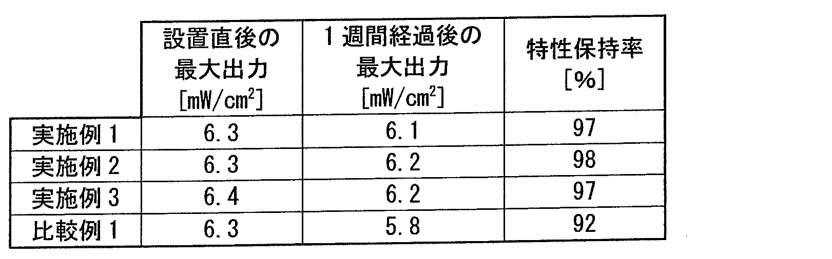
<評価>
表1に示すように、水平に対して20°以上の角度を為すとともに、正極側が負極側よりも鉛直方向に高くなるように色素増感太陽電池モジュールが設置された実施例1~3の太陽光発電装置の特性保持率[%]は、水平に対して20°以上の角度を為すとともに、負極側が正極側よりも鉛直方向に高くなるように色素増感太陽電池モジュールが設置された比較例1の太陽光発電装置の特性保持率[%]よりも高くなることが確認された。したがって、実施例1~3の太陽光発電装置は、比較例1の太陽光発電装置と比べて、水平に対して20°以上の角度を為すように設置した場合でも特性の低下を抑制することができることがわかる。
表1に示すように、水平に対して20°以上の角度を為すとともに、正極側が負極側よりも鉛直方向に高くなるように色素増感太陽電池モジュールが設置された実施例1~3の太陽光発電装置の特性保持率[%]は、水平に対して20°以上の角度を為すとともに、負極側が正極側よりも鉛直方向に高くなるように色素増感太陽電池モジュールが設置された比較例1の太陽光発電装置の特性保持率[%]よりも高くなることが確認された。したがって、実施例1~3の太陽光発電装置は、比較例1の太陽光発電装置と比べて、水平に対して20°以上の角度を為すように設置した場合でも特性の低下を抑制することができることがわかる。
<付記>
本発明の第1の態様によれば、光電変換素子の2つ以上が電気的に接続された光電変換モジュールを含み、光電変換素子は、基板と、基板上の第1導電層と、第1導電層上の光電変換層と、光電変換層上の第2導電層と、第1導電層上の電荷輸送層とを含み、光電変換層は、多孔質半導体層と、多孔質半導体層に吸着された光増感剤とを含み、電荷輸送層は、電解液を含み、光電変換モジュールは、水平に対して20°以上の角度を為すとともに、光電変換モジュールの正極側が負極側よりも鉛直方向に高くなるように設置されている光電変換装置を提供することができる。本発明の第1の態様の光電変換装置においては、光電変換モジュールの正極側が負極側よりも鉛直方向に高くなるように設置することによって、水平に対して20°以上の角度を為すように光電変換モジュールを設置した場合であっても光電変換装置の特性の低下を抑制することができる。
本発明の第1の態様によれば、光電変換素子の2つ以上が電気的に接続された光電変換モジュールを含み、光電変換素子は、基板と、基板上の第1導電層と、第1導電層上の光電変換層と、光電変換層上の第2導電層と、第1導電層上の電荷輸送層とを含み、光電変換層は、多孔質半導体層と、多孔質半導体層に吸着された光増感剤とを含み、電荷輸送層は、電解液を含み、光電変換モジュールは、水平に対して20°以上の角度を為すとともに、光電変換モジュールの正極側が負極側よりも鉛直方向に高くなるように設置されている光電変換装置を提供することができる。本発明の第1の態様の光電変換装置においては、光電変換モジュールの正極側が負極側よりも鉛直方向に高くなるように設置することによって、水平に対して20°以上の角度を為すように光電変換モジュールを設置した場合であっても光電変換装置の特性の低下を抑制することができる。
本発明の第1の態様の光電変換装置においては、第2導電層と電荷輸送層とが接していることが好ましい。この場合には、重力の影響により鉛直方向の下方に偏っているマイナスチャージを持つ電解液成分(たとえばヨウ化物イオン)を鉛直方向の上方に引き寄せることができるため、重力の影響による電解液成分の偏りを緩和することができる。
本発明の第1の態様の光電変換装置において、電荷輸送層は、第1導電層と第2導電層との間以外の領域に電解液が存在する部分を有することが好ましい。この場合には、電荷輸送層における第1導電層と第2導電層との間以外の領域に電解液が存在する部分によって、重力の影響による電解液成分の偏りをより緩和することができる。
本発明の第1の態様の光電変換装置において、電荷輸送層は、第1導電層と第2導電層との間以外の領域に電解液が存在する部分である第1電解液部と第2電解液部とを含み、第1電解液部は光電変換モジュールの正極側に位置し、第2電解液部は光電変換モジュールの負極側に位置しており、第1電解液部は、第2電解液部よりも厚い部分を有することが好ましい。この場合には、光電変換モジュールの鉛直方向のより高い位置に電解液を多く存在させることができるため、重力の影響による電解液成分の偏りをより緩和することができる。
本発明の第1の態様の光電変換装置において、電荷輸送層は、基板と、基板と向かい合う支持体と、支持体上の封止部とによって取り囲まれており、基板と支持体とが第1導電層上に設けられた絶縁層と支持体上に設けられた封止部との接合によって固定されていることが好ましい。この場合には、第1導電層と第2導電層との間以外の電荷輸送層の領域における電解液量を調節することができるため、光電変換モジュールの水平に対する傾きの角度に応じて、電解液部における電解液量を好適な量に柔軟に調節することができる。
本発明の第2の態様によれば、光電変換素子の2つ以上が電気的に接続された光電変換モジュールを準備する工程と、光電変換モジュールを水平に対して20°以上の角度を為すとともに、光電変換モジュールの正極側が負極側よりも鉛直方向に高くなるように設置する工程とを含み、光電変換素子は、基板と、基板上の第1導電層と、第1導電層上の光電変換層と、光電変換層上の第2導電層と、第1導電層上の電荷輸送層とを含み、光電変換層は、多孔質半導体層と、多孔質半導体層に吸着された光増感剤とを含み、電荷輸送層は電解液を含む光電変換装置の製造方法を提供することができる。本発明の第2の態様の光電変換装置においては、光電変換モジュールの正極側が負極側よりも鉛直方向に高くなるように設置することによって、水平に対して20°以上の角度を為すように光電変換モジュールを設置した場合であっても光電変換装置の特性の低下を抑制することができる。
以上のように本発明の実施の形態および実施例について説明を行なったが、上述の各実施の形態および各実施例の構成を適宜組み合わせることも当初から予定している。
今回開示された実施の形態および実施例はすべての点で例示であって制限的なものではないと考えられるべきである。本発明の範囲は上記した説明ではなくて請求の範囲によって示され、請求の範囲と均等の意味および範囲内でのすべての変更が含まれることが意図される。
本発明は、光電変換装置および光電変換装置の製造方法に利用することができ、特に、色素増感太陽電池モジュールを用いた太陽光発電装置とその製造方法に利用することができる。また、必要に応じて、光電変換装置とともに、インバーターや蓄電池などを設置して用いることができる。
1 光電変換モジュール、2 光電変換素子、3 設置面、11 基板、12 第1導電層、13 分離溝、14 光電変換層、14a 多孔質半導体層、15 多孔質絶縁層、16 触媒層、17 第2導電層、18 支持体、19 封止部、20 電荷輸送層、21a,21b 集電電極、22 絶縁層、31 光源、32 水平線。
Claims (5)
- 光電変換素子の2つ以上が電気的に接続された光電変換モジュールを含み、
前記光電変換素子は、基板と、前記基板上の第1導電層と、前記第1導電層上の光電変換層と、前記光電変換層上の第2導電層と、前記第1導電層上の電荷輸送層とを含み、
前記光電変換層は、多孔質半導体層と、前記多孔質半導体層に吸着された光増感剤とを含み、
前記電荷輸送層は、電解液を含み、
前記光電変換モジュールは、水平に対して20°以上の角度を為すとともに、前記光電変換モジュールの正極側が負極側よりも鉛直方向に高くなるように設置されている、光電変換装置。 - 前記電荷輸送層は、前記第1導電層と前記第2導電層との間以外の領域に、前記電解液が存在する部分を有する、請求項1に記載の光電変換装置。
- 前記電荷輸送層は、前記第1導電層と前記第2導電層との間以外の領域に前記電解液が存在する部分である第1電解液部と第2電解液部とを含み、
前記第1電解液部は前記光電変換モジュールの前記正極側に位置し、前記第2電解液部は前記光電変換モジュールの前記負極側に位置しており、
前記第1電解液部は、前記第2電解液部よりも厚い部分を有する、請求項2に記載の光電変換装置。 - 前記電荷輸送層は、前記基板と、前記基板と向かい合う支持体と、前記支持体上の封止部とによって取り囲まれており、前記基板と前記支持体とが前記第1導電層上に設けられた絶縁層と前記支持体上に設けられた前記封止部との接合によって固定されている、請求項1~請求項3のいずれか1項に記載の光電変換装置。
- 光電変換素子の2つ以上が電気的に接続された光電変換モジュールを準備する工程と、
前記光電変換モジュールを水平に対して20°以上の角度を為すとともに、前記光電変換モジュールの正極側が負極側よりも鉛直方向に高くなるように設置する工程とを含み、
前記光電変換素子は、基板と、前記基板上の第1導電層と、前記第1導電層上の光電変換層と、前記光電変換層上の第2導電層と、前記第1導電層上の電荷輸送層とを含み、
前記光電変換層は、多孔質半導体層と、前記多孔質半導体層に吸着された光増感剤とを含み、
前記電荷輸送層は、電解液を含む、光電変換装置の製造方法。
Applications Claiming Priority (2)
| Application Number | Priority Date | Filing Date | Title |
|---|---|---|---|
| JP2013207363 | 2013-10-02 | ||
| JP2013-207363 | 2013-10-02 |
Publications (1)
| Publication Number | Publication Date |
|---|---|
| WO2015049983A1 true WO2015049983A1 (ja) | 2015-04-09 |
Family
ID=52778578
Family Applications (1)
| Application Number | Title | Priority Date | Filing Date |
|---|---|---|---|
| PCT/JP2014/074497 Ceased WO2015049983A1 (ja) | 2013-10-02 | 2014-09-17 | 光電変換装置および光電変換装置の製造方法 |
Country Status (1)
| Country | Link |
|---|---|
| WO (1) | WO2015049983A1 (ja) |
Citations (6)
| Publication number | Priority date | Publication date | Assignee | Title |
|---|---|---|---|---|
| JP2009129686A (ja) * | 2007-11-22 | 2009-06-11 | Kiso Micro Kk | 太陽電池システム |
| JP2009302065A (ja) * | 2004-06-01 | 2009-12-24 | Konarka Technologies Inc | 太陽電池モジュール |
| JP2011222190A (ja) * | 2010-04-06 | 2011-11-04 | Sharp Corp | 湿式太陽電池および湿式太陽電池モジュール |
| WO2011155441A1 (ja) * | 2010-06-09 | 2011-12-15 | シャープ株式会社 | 湿式太陽電池および湿式太陽電池モジュール |
| JP2012019185A (ja) * | 2010-06-09 | 2012-01-26 | Sony Corp | 発電装置および発電方法 |
| US20120298187A1 (en) * | 2011-05-23 | 2012-11-29 | Hyun-Chul Kim | Photoelectric conversion module |
-
2014
- 2014-09-17 WO PCT/JP2014/074497 patent/WO2015049983A1/ja not_active Ceased
Patent Citations (6)
| Publication number | Priority date | Publication date | Assignee | Title |
|---|---|---|---|---|
| JP2009302065A (ja) * | 2004-06-01 | 2009-12-24 | Konarka Technologies Inc | 太陽電池モジュール |
| JP2009129686A (ja) * | 2007-11-22 | 2009-06-11 | Kiso Micro Kk | 太陽電池システム |
| JP2011222190A (ja) * | 2010-04-06 | 2011-11-04 | Sharp Corp | 湿式太陽電池および湿式太陽電池モジュール |
| WO2011155441A1 (ja) * | 2010-06-09 | 2011-12-15 | シャープ株式会社 | 湿式太陽電池および湿式太陽電池モジュール |
| JP2012019185A (ja) * | 2010-06-09 | 2012-01-26 | Sony Corp | 発電装置および発電方法 |
| US20120298187A1 (en) * | 2011-05-23 | 2012-11-29 | Hyun-Chul Kim | Photoelectric conversion module |
Similar Documents
| Publication | Publication Date | Title |
|---|---|---|
| JP5377327B2 (ja) | 光増感太陽電池モジュールおよびその製造方法 | |
| JP5422645B2 (ja) | 色素増感太陽電池および色素増感太陽電池モジュール | |
| JP4523549B2 (ja) | 色素増感太陽電池および色素増感太陽電池モジュール | |
| JP3717506B2 (ja) | 色素増感型太陽電池モジュール | |
| US9607772B2 (en) | Porous electrode, dye-sensitized solar cell, and dye-sensitized solar cell module | |
| JP5118233B2 (ja) | 光電変換素子および光電変換素子モジュール | |
| JP5171810B2 (ja) | 色素増感太陽電池モジュールおよびその製造方法 | |
| JPWO2011155441A1 (ja) | 湿式太陽電池および湿式太陽電池モジュール | |
| JP5657780B2 (ja) | 光電変換素子および光電変換モジュール | |
| JP4448478B2 (ja) | 色素増感型太陽電池モジュール | |
| JP5536015B2 (ja) | 光電変換素子および光電変換素子モジュール | |
| WO2014038570A1 (ja) | 光電変換素子、その製造方法、光電変換素子モジュールおよびその製造方法 | |
| JP5758400B2 (ja) | 色素増感太陽電池モジュールおよびその製造方法 | |
| WO2013114733A1 (ja) | 光電変換素子モジュール | |
| WO2012086377A1 (ja) | 色素増感太陽電池および色素増感太陽電池モジュールならびにその製造方法 | |
| JP2014229434A (ja) | 光電変換素子および色素増感太陽電池 | |
| JP2013200960A (ja) | 光電変換素子モジュールおよびその製造方法 | |
| JP5313278B2 (ja) | 光電変換素子および光電変換素子モジュール | |
| US10916382B2 (en) | Photoelectric conversion element and photoelectric conversion element module | |
| WO2013161557A1 (ja) | 光電変換素子モジュールおよびその製造方法 | |
| WO2015049983A1 (ja) | 光電変換装置および光電変換装置の製造方法 | |
| JP5480234B2 (ja) | 光電変換素子および光電変換素子の製造方法 | |
| JP2013251229A (ja) | 光電変換素子および色素増感太陽電池 | |
| JP2013251228A (ja) | 光電変換素子および色素増感太陽電池 | |
| WO2015133030A1 (ja) | 光電変換モジュールおよびそれを用いた電子機器 |
Legal Events
| Date | Code | Title | Description |
|---|---|---|---|
| 121 | Ep: the epo has been informed by wipo that ep was designated in this application |
Ref document number: 14851350 Country of ref document: EP Kind code of ref document: A1 |
|
| NENP | Non-entry into the national phase |
Ref country code: DE |
|
| 122 | Ep: pct application non-entry in european phase |
Ref document number: 14851350 Country of ref document: EP Kind code of ref document: A1 |
|
| NENP | Non-entry into the national phase |
Ref country code: JP |