WO2015049929A1 - 立体表示装置 - Google Patents
立体表示装置 Download PDFInfo
- Publication number
- WO2015049929A1 WO2015049929A1 PCT/JP2014/071777 JP2014071777W WO2015049929A1 WO 2015049929 A1 WO2015049929 A1 WO 2015049929A1 JP 2014071777 W JP2014071777 W JP 2014071777W WO 2015049929 A1 WO2015049929 A1 WO 2015049929A1
- Authority
- WO
- WIPO (PCT)
- Prior art keywords
- liquid crystal
- substrate
- electrode
- display device
- crystal panel
- Prior art date
- Legal status (The legal status is an assumption and is not a legal conclusion. Google has not performed a legal analysis and makes no representation as to the accuracy of the status listed.)
- Ceased
Links
Images






















Classifications
-
- G—PHYSICS
- G02—OPTICS
- G02B—OPTICAL ELEMENTS, SYSTEMS OR APPARATUS
- G02B30/00—Optical systems or apparatus for producing three-dimensional [3D] effects, e.g. stereoscopic images
- G02B30/20—Optical systems or apparatus for producing three-dimensional [3D] effects, e.g. stereoscopic images by providing first and second parallax images to an observer's left and right eyes
- G02B30/26—Optical systems or apparatus for producing three-dimensional [3D] effects, e.g. stereoscopic images by providing first and second parallax images to an observer's left and right eyes of the autostereoscopic type
- G02B30/27—Optical systems or apparatus for producing three-dimensional [3D] effects, e.g. stereoscopic images by providing first and second parallax images to an observer's left and right eyes of the autostereoscopic type involving lenticular arrays
-
- G—PHYSICS
- G02—OPTICS
- G02B—OPTICAL ELEMENTS, SYSTEMS OR APPARATUS
- G02B30/00—Optical systems or apparatus for producing three-dimensional [3D] effects, e.g. stereoscopic images
- G02B30/20—Optical systems or apparatus for producing three-dimensional [3D] effects, e.g. stereoscopic images by providing first and second parallax images to an observer's left and right eyes
- G02B30/26—Optical systems or apparatus for producing three-dimensional [3D] effects, e.g. stereoscopic images by providing first and second parallax images to an observer's left and right eyes of the autostereoscopic type
- G02B30/30—Optical systems or apparatus for producing three-dimensional [3D] effects, e.g. stereoscopic images by providing first and second parallax images to an observer's left and right eyes of the autostereoscopic type involving parallax barriers
- G02B30/31—Optical systems or apparatus for producing three-dimensional [3D] effects, e.g. stereoscopic images by providing first and second parallax images to an observer's left and right eyes of the autostereoscopic type involving parallax barriers involving active parallax barriers
-
- G—PHYSICS
- G02—OPTICS
- G02F—OPTICAL DEVICES OR ARRANGEMENTS FOR THE CONTROL OF LIGHT BY MODIFICATION OF THE OPTICAL PROPERTIES OF THE MEDIA OF THE ELEMENTS INVOLVED THEREIN; NON-LINEAR OPTICS; FREQUENCY-CHANGING OF LIGHT; OPTICAL LOGIC ELEMENTS; OPTICAL ANALOGUE/DIGITAL CONVERTERS
- G02F1/00—Devices or arrangements for the control of the intensity, colour, phase, polarisation or direction of light arriving from an independent light source, e.g. switching, gating or modulating; Non-linear optics
- G02F1/01—Devices or arrangements for the control of the intensity, colour, phase, polarisation or direction of light arriving from an independent light source, e.g. switching, gating or modulating; Non-linear optics for the control of the intensity, phase, polarisation or colour
- G02F1/13—Devices or arrangements for the control of the intensity, colour, phase, polarisation or direction of light arriving from an independent light source, e.g. switching, gating or modulating; Non-linear optics for the control of the intensity, phase, polarisation or colour based on liquid crystals, e.g. single liquid crystal display cells
- G02F1/133—Constructional arrangements; Operation of liquid crystal cells; Circuit arrangements
- G02F1/1333—Constructional arrangements; Manufacturing methods
- G02F1/1343—Electrodes
- G02F1/134309—Electrodes characterised by their geometrical arrangement
-
- H—ELECTRICITY
- H04—ELECTRIC COMMUNICATION TECHNIQUE
- H04N—PICTORIAL COMMUNICATION, e.g. TELEVISION
- H04N13/00—Stereoscopic video systems; Multi-view video systems; Details thereof
- H04N13/30—Image reproducers
- H04N13/302—Image reproducers for viewing without the aid of special glasses, i.e. using autostereoscopic displays
- H04N13/31—Image reproducers for viewing without the aid of special glasses, i.e. using autostereoscopic displays using parallax barriers
-
- H—ELECTRICITY
- H04—ELECTRIC COMMUNICATION TECHNIQUE
- H04N—PICTORIAL COMMUNICATION, e.g. TELEVISION
- H04N13/00—Stereoscopic video systems; Multi-view video systems; Details thereof
- H04N13/30—Image reproducers
- H04N13/302—Image reproducers for viewing without the aid of special glasses, i.e. using autostereoscopic displays
- H04N13/31—Image reproducers for viewing without the aid of special glasses, i.e. using autostereoscopic displays using parallax barriers
- H04N13/312—Image reproducers for viewing without the aid of special glasses, i.e. using autostereoscopic displays using parallax barriers the parallax barriers being placed behind the display panel, e.g. between backlight and spatial light modulator [SLM]
-
- H—ELECTRICITY
- H04—ELECTRIC COMMUNICATION TECHNIQUE
- H04N—PICTORIAL COMMUNICATION, e.g. TELEVISION
- H04N13/00—Stereoscopic video systems; Multi-view video systems; Details thereof
- H04N13/30—Image reproducers
- H04N13/366—Image reproducers using viewer tracking
-
- H—ELECTRICITY
- H04—ELECTRIC COMMUNICATION TECHNIQUE
- H04N—PICTORIAL COMMUNICATION, e.g. TELEVISION
- H04N13/00—Stereoscopic video systems; Multi-view video systems; Details thereof
- H04N13/30—Image reproducers
- H04N13/366—Image reproducers using viewer tracking
- H04N13/376—Image reproducers using viewer tracking for tracking left-right translational head movements, i.e. lateral movements
-
- H—ELECTRICITY
- H04—ELECTRIC COMMUNICATION TECHNIQUE
- H04N—PICTORIAL COMMUNICATION, e.g. TELEVISION
- H04N13/00—Stereoscopic video systems; Multi-view video systems; Details thereof
- H04N13/30—Image reproducers
- H04N13/398—Synchronisation thereof; Control thereof
-
- H—ELECTRICITY
- H04—ELECTRIC COMMUNICATION TECHNIQUE
- H04N—PICTORIAL COMMUNICATION, e.g. TELEVISION
- H04N2213/00—Details of stereoscopic systems
- H04N2213/001—Constructional or mechanical details
Definitions
- the present invention relates to an autostereoscopic display device.
- a parallax barrier method and a lenticular lens method are known. These stereoscopic display devices separate light with a barrier or a lens, project different images to the left and right eyes, and give the viewer a stereoscopic effect. 2. Description of the Related Art In recent years, autostereoscopic display devices that are on the market are mainly two-view parallax barrier systems and lenticular lens systems.
- a good stereoscopic display can be obtained in the set region.
- the image to be projected on the right eye and the image to be projected on the left eye are mixed and doubled.
- a multi-viewpoint technique and a tracking technique for detecting the position of the observer's head and displaying an image in accordance with the position have been proposed.
- SW-LCD barrier division switch liquid crystal display
- Japanese Patent Laid-Open No. 2013-24957 includes a display panel in which subpixel pairs are arranged in the horizontal direction, and a parallax barrier shutter panel in which sub-openings capable of switching between a light transmission state and a light shielding state are arranged in the horizontal direction.
- a display device is described. In this display device, among a plurality of sub-openings belonging to the reference parallax barrier pitch, an arbitrary number of sub-openings adjacent to each other are set in a light-transmitting state, and the remaining sub-openings are set in a light-shielding state. Formed on a parallax barrier shutter panel.
- the sub opening pitch is equal to or smaller than the difference between the sub pixel width and the total opening width.
- the subpixel aperture pitch In order to satisfy the conditions described in Japanese Patent Laid-Open No. 2013-24957, the subpixel aperture pitch must be reduced. In order to reduce the sub-pixel opening pitch, it is necessary to increase the number of electrodes of the parallax barrier shutter panel. However, when the number of electrodes of the parallax barrier shutter panel is increased, another problem may be caused thereby, which is limited.
- An object of the present invention is to obtain a configuration of a stereoscopic display device that can maintain crosstalk in a low state even when an observer moves.
- a stereoscopic display device disclosed herein includes a display panel that displays an image, a switch liquid crystal panel that is arranged on the display panel, a position sensor that acquires position information of an observer, and a predetermined alignment direction.
- a control unit configured to move a parallax barrier in which a transmissive region and a non-transmissive region are periodically formed along the alignment direction according to the position information and to display the parallax barrier on the switch liquid crystal panel.
- the switch liquid crystal panel includes a liquid crystal layer having a refractive index anisotropy ⁇ n of liquid crystal molecules of 0.14 or less, a first substrate and a second substrate facing each other with the liquid crystal layer interposed therebetween, and the first substrate and the first substrate. And an electrode group including a plurality of electrodes formed on at least one of the two substrates and arranged along the alignment direction.
- FIG. 1 is a schematic cross-sectional view showing a configuration of a stereoscopic display device according to the first embodiment of the present invention.
- FIG. 2 is a block diagram illustrating a functional configuration of the stereoscopic display device according to the first embodiment of the present invention.
- FIG. 3 is a flowchart of a process performed by the stereoscopic display device according to the first embodiment of the present invention.
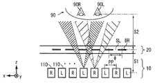
- FIG. 4A is a diagram for explaining the principle of stereoscopic display by the stereoscopic display device according to the first embodiment of the present invention.
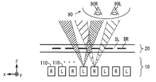
- FIG. 4B is a diagram for explaining the principle of stereoscopic display by the stereoscopic display device according to the first embodiment of the present invention.
- FIG. 4A is a diagram for explaining the principle of stereoscopic display by the stereoscopic display device according to the first embodiment of the present invention.
- FIG. 4B is a diagram for explaining the principle of stereoscopic display by the stereoscopic display device according to the first embodiment of the present invention
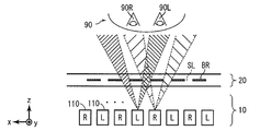
- FIG. 4C is a diagram for explaining the principle of stereoscopic display by the stereoscopic display device according to the first embodiment of the present invention.
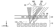
- FIG. 5A is a diagram for explaining the principle of stereoscopic display by the stereoscopic display device according to the first embodiment of the present invention.
- FIG. 5B is a diagram for explaining the principle of stereoscopic display by the stereoscopic display device according to the first embodiment of the present invention.
- FIG. 5C is a view for explaining the principle of stereoscopic display by the stereoscopic display device according to Embodiment 1 of the present invention.
- FIG. 6A is a plan view showing the configuration of the first substrate of the switch liquid crystal panel.
- FIG. 6B is a plan view showing the configuration of the second substrate of the switch liquid crystal panel.
- FIG. 6A is a plan view showing the configuration of the first substrate of the switch liquid crystal panel.
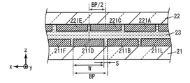
- FIG. 7 is a cross-sectional view illustrating a schematic configuration of the stereoscopic display device according to the first embodiment of the present invention.
- FIG. 8 is an enlarged sectional view showing a part of the switch liquid crystal panel.
- FIG. 9 is a graph showing the relationship between the retardation ⁇ n ⁇ d of the liquid crystal layer and the transmittance of the liquid crystal layer.
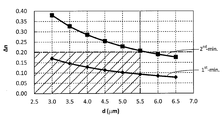
- FIG. 10A shows that retardation ⁇ n ⁇ d is 1 st -min. Or 2 nd -min. Is a table showing the relationship between the cell thickness d and the refractive index anisotropy ⁇ n.
- FIG. 10B shows that retardation ⁇ n ⁇ d is 1 st ⁇ min. Or 2 nd -min.
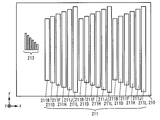
- FIG. 11A is a diagram for explaining an example of a method of manufacturing the first substrate.
- FIG. 11B is a diagram for explaining an example of a method of manufacturing the first substrate.
- FIG. 11C is a diagram for explaining an example of a method of manufacturing the first substrate.
- FIG. 12 is a cross-sectional view schematically showing one of the barrier lighting states of the switch liquid crystal panel.
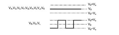
- FIG. 13A is an example of a waveform diagram of signals V A to V L supplied to each electrode in order to set the switch liquid crystal panel to the barrier lighting state of FIG. FIG.
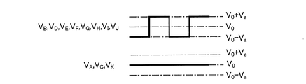
- FIG. 13B is another example of a waveform diagram of signals V A to V L supplied to the respective electrodes to bring the switch liquid crystal panel into the barrier lighting state of FIG.
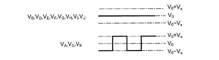
- FIG. 13C is still another example of a waveform diagram of signals V A to V L supplied to each electrode in order to set the switch liquid crystal panel to the barrier lighting state of FIG.
- FIG. 14 is a cross-sectional view schematically showing another one of the barrier lighting states of the switch liquid crystal panel.
- FIG. 15A is an example of a waveform diagram of signals V A to V L supplied to each electrode in order to set the switch liquid crystal panel to the barrier lighting state of FIG.
- FIG. 15B is another example of a waveform diagram of signals V A to V L supplied to the respective electrodes to bring the switch liquid crystal panel into the barrier lighting state of FIG.
- FIG. 15C is still another example of a waveform diagram of signals V A to V L supplied to the respective electrodes to bring the switch liquid crystal panel into the barrier lighting state of FIG.
- FIG. 16A is a cross-sectional view schematically showing one of the barrier lighting states of the switch liquid crystal panel when the refractive index anisotropy ⁇ n of the liquid crystal molecules is large.
- FIG. 16B is a cross-sectional view schematically showing one of the barrier lighting states of the switch liquid crystal panel when the refractive index anisotropy ⁇ n of the liquid crystal molecules is small.
- FIG. 16C is a graph simulating the distribution of the orientation of liquid crystal molecules and the distribution of retardation ⁇ n ⁇ d.
- FIG. 17 is a cross-sectional view illustrating a schematic configuration of a stereoscopic display device according to the second embodiment of the present invention.
- FIG. 18 is an enlarged sectional view showing a part of the switch liquid crystal panel.
- FIG. 19 is a cross-sectional view schematically showing another one of the barrier lighting states of the switch liquid crystal panel.
- FIG. 20A is an example of a waveform diagram of signals V COM and V A to V L supplied to each electrode in order to set the switch liquid crystal panel to the barrier lighting state of FIG.
- FIG. 20B is another example of waveform diagrams of signals V COM and V A to V L supplied to the respective electrodes to bring the switch liquid crystal panel into the barrier lighting state of FIG.
- FIG. 20C is still another example of waveform diagrams of signals V COM and V A to V L supplied to the respective electrodes for setting the switch liquid crystal panel to the barrier lighting state of FIG.
- FIG. 21A is a cross-sectional view schematically showing one of the barrier lighting states of the switch liquid crystal panel when the refractive index anisotropy ⁇ n of the liquid crystal molecules is large.
- FIG. 21B is a cross-sectional view schematically showing one of the barrier lighting states of the switch liquid crystal panel when the refractive index anisotropy ⁇ n of the liquid crystal molecules is small.
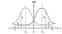
- FIG. 22 is a diagram illustrating the angular characteristics of the luminance of the stereoscopic display device when the barrier lighting state is fixed.
- FIG. 21A is a cross-sectional view schematically showing one of the barrier lighting states of the switch liquid crystal panel when the refractive index anisotropy ⁇ n of the liquid crystal molecules is large.
- FIG. 21B is a cross-sectional view schematically showing one of the
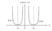
- FIG. 23 is a diagram illustrating angular characteristics of the left-eye crosstalk XT (L) and the right-eye crosstalk XT (R).
- FIG. 24 is a table showing the relationship between the parameters of the five types of stereoscopic display devices and the crosstalk XT (%).
- FIG. 25 is a graph showing the relationship between the refractive index anisotropy ⁇ n and the crosstalk XT.
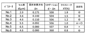
- FIG. 26 is a table showing the relationship among parameters of six types of stereoscopic display devices, crosstalk XT (%), and followability.
- FIG. 27 is a table showing the relationship between the parameters of the five types of stereoscopic display devices and the crosstalk XT (%).
- a stereoscopic display device includes a display panel that displays an image, a switch liquid crystal panel that is placed on the display panel, a position sensor that acquires position information of an observer, and a predetermined alignment direction. And a control unit that moves the parallax barrier in which the transmissive region and the non-transmissive region are periodically formed along the alignment direction according to the position information and displays the parallax barrier on the switch liquid crystal panel.
- the switch liquid crystal panel includes a liquid crystal layer having a refractive index anisotropy ⁇ n of 0.14 or less, a first substrate and a second substrate facing each other with the liquid crystal layer interposed therebetween, and at least one of the first substrate and the second substrate. And an electrode group including a plurality of electrodes arranged along the alignment direction (first configuration).
- the switch liquid crystal panel is arranged so as to overlap the display panel.
- a parallax barrier in which a transmissive region and a non-transmissive region are periodically formed along a predetermined alignment direction is displayed.
- control unit moves the parallax barrier along the alignment direction and displays the parallax barrier on the switch liquid crystal panel according to the position information of the observer acquired by the position sensor.
- the crosstalk can be kept low.
- the switch liquid crystal panel moves the parallax barrier by controlling the orientation of the liquid crystal molecules in the liquid crystal layer by changing the potentials of the plurality of electrodes included in the electrode group. Therefore, the electrode group is preferably composed of many electrodes.
- the refractive index anisotropy ⁇ n of the liquid crystal molecules in the liquid crystal layer is set to 0.14 or less. As a result, even when the proportion of voids is large, the influence can be reduced. As a result, the crosstalk can be kept low.
- the switch liquid crystal panel is preferably normally white (second configuration).
- the retardation of the liquid crystal layer is preferably set to the first minimum (third configuration).
- the thickness of the liquid crystal layer is preferably 5.5 ⁇ m or less (fourth configuration).
- the alignment direction of the liquid crystal molecules on the first substrate side and the alignment direction of the liquid crystal molecules on the second substrate side are mutually different. It is preferable that the angle differs by 90 ° (fifth configuration).
- the transmittance of the switch liquid crystal panel can be improved.
- the electrode group is formed on the first substrate and includes a first electrode group including a plurality of electrodes arranged at predetermined intervals along the alignment direction, and the second substrate. And a second electrode group including a plurality of electrodes arranged at the predetermined interval along the alignment direction, wherein the first electrode group and the second electrode group have the predetermined interval from each other in the alignment direction. It is preferable that they are shifted by half (sixth configuration).
- the parallax barrier can be moved with the half interval between the electrodes as a minimum unit.
- the electrode group is formed on the first substrate, and includes a first electrode group including a plurality of electrodes arranged at predetermined intervals along the alignment direction, and the second substrate. It may be configured to include a common electrode formed on the entire surface (seventh configuration).
- the switch liquid crystal panel may be disposed closer to the observer than the display panel (eighth configuration).
- the light from the display panel is separated by the switch liquid crystal panel.
- This configuration is superior in separation characteristics compared to the following ninth configuration.
- the display panel may be arranged closer to the viewer than the switch liquid crystal panel (9th configuration).
- the light separated by the switch liquid crystal panel passes through the display panel.
- the light separated by the switch liquid crystal panel is scattered or diffracted by the display panel.
- the crosstalk is worse than the configuration in which the switch liquid crystal panel is arranged closer to the viewer than the display panel, but the angle change of the brightness becomes gentle.
- the display panel may be a liquid crystal display panel (tenth configuration).
- FIG. 1 is a schematic cross-sectional view showing a configuration of a stereoscopic display device 1 according to the first embodiment of the present invention.
- the stereoscopic display device 1 includes a display panel 10, a switch liquid crystal panel 20, and an adhesive resin 30.
- the display panel 10 and the switch liquid crystal panel 20 are arranged so that the switch liquid crystal panel 20 is on the viewer 90 side, and are bonded together by an adhesive resin 30.
- the display panel 10 includes a TFT (Thin Film Transistor) substrate 11, a CF (Color Filter) substrate 12, a liquid crystal layer 13, and polarizing plates 14 and 15.
- the display panel 10 controls the TFT substrate 11 and the CF substrate 12 to manipulate the orientation of the liquid crystal molecules in the liquid crystal layer 13 to display an image.
- the switch liquid crystal panel 20 includes a first substrate 21, a second substrate 22, a liquid crystal layer 23, and a polarizing plate 24.
- the first substrate 21 and the second substrate 22 are arranged so as to face each other.
- the liquid crystal layer 23 is sandwiched between the first substrate 21 and the second substrate 22.
- the polarizing plate 24 is disposed on the viewer 90 side.
- the switch liquid crystal panel 20 controls the potential of these electrodes, manipulates the orientation of the liquid crystal molecules in the liquid crystal layer 23, and changes the behavior of light passing through the liquid crystal layer 23. More specifically, the switch liquid crystal panel 23 includes a non-transmissive region (barrier) that blocks light from the backlight by the alignment of the liquid crystal molecules of the liquid crystal layer 23 and the action of the polarizing plate 15 and the polarizing plate 24, and the backlight. And a transmissive region (slit) that transmits light from the light. Detailed structures and operations of the first substrate 21 and the second substrate 22 will be described later.
- the thickness of the TFT substrate 11 and the CF substrate 12 is, for example, 200 ⁇ m.
- the thickness of the polarizing plate 14 is, for example, 137 ⁇ m.
- the thickness of the polarizing plate 15 is 170 ⁇ m, for example.
- the thickness of the first substrate 21 and the second substrate 22 is, for example, 225 ⁇ m.
- the thickness of the adhesive resin 30 is, for example, 50 ⁇ m.
- the polarizing plate 15 may be disposed on the switch liquid crystal panel 20. That is, the polarizing plate 15 may be disposed on the surface of the switch liquid crystal panel 20 on the display panel 10 side of the first substrate 21, and the adhesive resin 30 may be disposed between the polarizing plate 15 and the CF substrate 12.
- the direction parallel to the line segment connecting the left eye 90L and the right eye 90R of the observer 90 when the observer 90 and the stereoscopic display device 1 face each other (the x direction in FIG. 1) is referred to as a horizontal direction.
- a direction (y direction in FIG. 1) perpendicular to the horizontal direction in the plane of the display panel 10 is referred to as a vertical direction.
- FIG. 2 is a block diagram showing a functional configuration of the stereoscopic display device 1.
- FIG. 3 is a flowchart of processing by the stereoscopic display device 1.
- the stereoscopic display device 1 further includes a control unit 40 and a position sensor 41.
- the control unit 40 includes a calculation unit 42, a switch liquid crystal panel drive unit 43, and a display panel drive unit 44.
- the display panel drive unit 44 drives the display panel 10 based on a video signal input from the outside, and causes the display panel 10 to display an image.
- the position sensor 41 acquires the position information of the observer 90 (step S1).
- the position sensor 41 is, for example, a camera or an infrared sensor.
- the position sensor 41 supplies the acquired position information to the calculation unit 42 of the control unit 40.
- the calculation unit 42 analyzes the position information of the observer 90 supplied from the position sensor 41, and calculates the position coordinates (x, y, z) of the observer 90 (step S2).
- the position coordinates can be calculated by, for example, an eye tracking system that detects the position of the eyes of the observer 90 by image processing.
- the calculation of the position coordinates may be performed by a head tracking system that detects the position of the head of the observer 90 using infrared rays.
- the calculation unit 42 further determines the barrier lighting state of the switch liquid crystal panel 20 according to the position coordinates of the observer 90 (step S3). That is, the position of the barrier of the switch liquid crystal panel 20 and the position of the slit are determined according to the position coordinates of the observer 90.
- the calculation unit 42 supplies the information on the determined barrier lighting state to the switch liquid crystal panel drive unit 43.
- the switch liquid crystal panel drive unit 43 drives the switch liquid crystal panel 20 based on the information supplied from the calculation unit 42 (step S4). Thereafter, steps S1 to S4 are repeated.
- the display panel 10 includes a plurality of pixels 110. On the pixel 110, the right-eye image (R) and the left-eye image (L) are alternately displayed in the horizontal direction.
- the switch liquid crystal panel 20 is formed with a barrier BR that blocks light from the display panel 10 and a slit SL that transmits light from the display panel 10 at predetermined intervals.
- a barrier BR that blocks light from the display panel 10
- a slit SL that transmits light from the display panel 10 at predetermined intervals.
- interval PP between the pixels 110 and the interval ⁇ between the barrier BRs are defined such that the distance from the display surface of the display panel 10 to the barrier BR is S1, the distance from the barrier BR to the observer 90 is S2, and S2 is relative to S1.
- S1 the distance from the barrier BR to the observer 90 is S2
- S2 is relative to S1.
- FIG. 4B is a diagram illustrating a state in which the observer 90 has moved from FIG. 4A in the horizontal direction.
- both the right-eye image (R) and the left-eye image (L) appear in the right eye 90R of the observer 90.
- both the right-eye image (R) and the left-eye image (L) appear in the left eye 90L. That is, crosstalk occurs, and the observer 90 cannot feel a stereoscopic effect.
- FIG. 4C is a diagram showing a state where the observer 90 has moved further in the horizontal direction from FIG. 4B.
- the left-eye image (L) appears in the right eye 90R of the observer 90
- the right-eye image (R) appears in the left eye 90L.
- the viewer 90 since the video image that should be in the back is observed in the foreground and the video image that should be in the foreground is observed in the back, the viewer 90 cannot feel the correct stereoscopic effect and feels uncomfortable. Will be given.
- the control unit 40 changes the barrier lighting state of the switch liquid crystal panel 20 according to the position information (position coordinates) of the observer 90. Accordingly, the observer 90 can always feel a three-dimensional effect, and crosstalk and a reverse viewing state can be prevented from occurring.
- FIG. 6A is a plan view showing the configuration of the first substrate 21 of the switch liquid crystal panel 20.
- a first electrode group 211 is formed on the first substrate 21.
- the first electrode group 211 includes a plurality of electrodes arranged at an electrode interval BP along the x direction. Each of the plurality of electrodes extends in the y direction and is arranged in parallel to each other.
- a wiring group 212 electrically connected to the first electrode group 211 is formed on the first substrate 21.
- the wiring group 212 is preferably formed outside a portion (active area AA) that overlaps the display area of the display panel 10 when the switch liquid crystal panel 20 is overlapped with the display panel 10.
- FIG. 6B is a plan view showing the configuration of the second substrate 22 of the switch liquid crystal panel 20.
- a second electrode group 221 is formed on the second substrate 22.
- the second electrode group 221 includes a plurality of electrodes arranged at the electrode interval BP along the x direction. Each of the plurality of electrodes extends in the y direction and is arranged in parallel to each other.
- a wiring group 222 electrically connected to the second electrode group 221 is formed on the second substrate 22. Similar to the wiring group 212, the wiring group 222 is preferably formed outside the active area AA.
- Twelve systems of signals V A to V L are supplied from the control unit 40 to the first electrode group 211 and the second electrode group 221. More specifically, six signals V B , V D , V F , V H , V J , and V L are supplied to the first electrode group 211 through the wiring group 212. Six systems of signals V A , V C , V E , V G , V I , and V K are supplied to the second electrode group 221 through the wiring group 222.
- the electrodes each electrode 211B that V L is supplied 211D, 211F, 211H, 211J, 211L
- wirings electrically connected to the electrodes 211B, 211D, 211F, 211H, 211J, and 211L are referred to as wirings 212B, 212D, 212F, 212H, 212J, and 212L for reference.
- electrodes to which signals V A , V C , V E , V G , V I , and V K are supplied are electrodes 221A, 221C, 221E, 221G, 221I, and 221K, respectively. Call and refer.
- the wirings electrically connected to the electrodes 221A, 221C, 221E, 221G, 221I, and 221K are referred to as wirings 222A, 222C, 222E, 222G, 222I, and 222K.
- the electrodes 211B, 211D, 211F, 211H, 211J, and 211L are periodically arranged in this order in the x direction. In other words, six electrodes adjacent to a certain electrode are arranged so as to be supplied with the same signal as that electrode. Similarly, the electrodes 221A, 221C, 221E, 221G, 221I, and 221K are periodically arranged in the x direction in this order.
- FIG. 7 is a cross-sectional view showing a schematic configuration of the stereoscopic display device 1.
- FIG. 8 is an enlarged cross-sectional view showing a part of the switch liquid crystal panel 20.
- the first electrode group 211 and the second electrode group 221 are arranged so as to be shifted from each other in the x direction.
- the first electrode group 211 and the second electrode group 221 are preferably arranged so as to be shifted from each other by half the electrode interval BP in the x direction, as in the example of FIG.
- the electrode interval BP is the sum of the electrode width W and the gap S between the electrodes.
- BP ⁇ / 6 ⁇ PP / 3.
- alignment films are formed on the first substrate 21 and the second substrate 22, respectively.
- the alignment film formed on the first substrate 21 and the alignment film formed on the second substrate 22 are rubbed in directions intersecting each other.
- the liquid crystal molecules of the liquid crystal layer 23 are in a so-called twisted nematic alignment in which the alignment direction rotates from the first substrate 21 toward the second substrate 22 in the absence of voltage.
- the switch liquid crystal panel 20 is a so-called normally white liquid crystal in which the transmittance is maximized when no voltage is applied to the liquid crystal layer 23.
- the switch liquid crystal panel 20 it is preferable to employ a twisted nematic having a high transmittance as the alignment film. Moreover, it is preferable to employ normally white as the arrangement of the polarizing plates. This is because the normally white liquid crystal is in a state in which no voltage is applied in the two-dimensional display mode in which stereoscopic display is not performed, and thus power consumption can be reduced.
- FIG. 9 is a graph showing the relationship between the retardation ⁇ n ⁇ d of the liquid crystal layer 23 and the transmittance of the liquid crystal layer 23.
- the calculation is made assuming that the twist angle ⁇ of the liquid crystal layer 23 is 90 ° and the wavelength of light ⁇ is 589.
- the twist angle is ⁇
- the thickness (cell thickness) of the liquid crystal layer 23 is d
- the wavelength of light is ⁇
- the retardation ⁇ n ⁇ d is expressed by the following formula:
- the transmittance is maximized.
- m is an integer.
- ⁇ n ⁇ d (m 2 ⁇ ( ⁇ / ⁇ ) 2 ) 1/2 ⁇ ⁇
- FIG. 10A shows that retardation ⁇ n ⁇ d is 1 st -min. Or 2 nd -min. Is a table showing the relationship between the cell thickness d (first row) and the refractive index anisotropy ⁇ n (second and third rows).
- FIG. 10B shows that retardation ⁇ n ⁇ d is 1 st ⁇ min. Or 2 nd -min. Is a table showing the relationship between the cell thickness d and the refractive index anisotropy ⁇ n.
- the refractive index anisotropy ⁇ n exceeds 0.2, the light resistance and reliability of liquid crystal molecules deteriorate. If the refractive index anisotropy ⁇ n exceeds 0.2, the transmittance of the liquid crystal itself is lowered. Therefore, the refractive index anisotropy ⁇ n is preferably 0.2 or less.
- the cell thickness d is increased, the response speed of the switch liquid crystal panel 20 is decreased, and the followability during tracking is deteriorated. As a result, luminance changes and crosstalk can be easily seen. Therefore, it is preferable that the cell thickness d is small.
- a preferable cell thickness d is 5.5 ⁇ m or less.
- the refractive index anisotropy ⁇ n is preferably 0.2 or less and the cell thickness d is preferably 5.5 ⁇ m or less.
- FIG. 10 schematically shows this range with hatching.
- the retardation ⁇ n ⁇ d is 1 st ⁇ min. It is preferable to set to.
- the retardation ⁇ n ⁇ d in the case of a twisted nematic liquid crystal is preferably 330 to 650 nm, more preferably 380 to 650 nm, and further preferably 440 to 580 nm.
- the second substrate 22 can have the same configuration as the first substrate 21 and can be manufactured in the same manner as the first substrate 21.
- a first electrode group 211 and a relay electrode 213 are formed on a substrate 210.
- the relay electrode 213 is an electrode for relaying the wiring group 212 formed in a later process.
- the substrate 210 is a substrate having translucency and insulating properties, for example, a glass substrate.
- the first electrode group 211 preferably has translucency.
- the relay electrode 213 is formed in the active area, it is preferable that the relay electrode 213 also has translucency.
- the relay electrode 213 is not required to have translucency.
- the first electrode group 211 and the relay electrode 213 are, for example, ITO (Indium Tin Oxide).
- the relay electrode 213 When the relay electrode 213 is formed outside the active area, the relay electrode 213 may be aluminum, for example.
- the first electrode group 211 and the relay electrode 213 are formed by sputtering or CVD (Chemical Vapor Deposition), for example, and patterned by photolithography.
- an insulating film 214 is formed to cover the substrate 210, the first electrode group 211, and the relay electrode 213.
- a contact hole 214a and a contact hole 214b are formed in the insulating film 214.
- the contact hole 214a is formed at a position where the first electrode group 211 and the wiring group 212 formed in the next step are connected.
- the contact hole 214b is formed at a position where the relay electrode 213 and the wiring group 212 are connected.
- the insulating film 214 preferably has translucency, for example, SiN.
- the insulating film 214 is formed by, for example, CVD, and the contact hole 214a and the contact hole 214b are formed by photolithography. In the case where the wiring group 212 is formed outside the active area, patterning may be performed so that the insulating film 214 is formed only outside the active area.
- a wiring group 212 is formed.
- the wiring group 212 is connected to the first electrode group 211 through the contact hole 214a, and is connected to the relay electrode 213 through the contact hole 214b.
- the wiring group 212 preferably has high conductivity, for example, aluminum.
- the wiring group 212 may be ITO.
- the wiring group 212 is formed by sputtering and patterned by photolithography.
- the wirings 212B, 212D, 212F, 212H, 212J, and 212L are connected to the electrodes 211B, 211D, 211F, 211H, 211J, and 211L, respectively.
- the first electrode group 211 and the wiring group 212 can be crossed in a plan view.
- one end portion of the wiring group 212 is gathered in the vicinity of the peripheral portion of the substrate 21 to form a terminal portion 212a.
- An FPC (Flexible Printed Circuit) or the like is connected to the terminal portion 212a.
- wirings are connected to both sides of each electrode of the electrode group 211 in the y direction.
- a set of wirings connected to both sides of each electrode in the electrode group 211 in the y direction are connected to each other by a relay electrode 213.
- FIG. 12 is a cross-sectional view schematically showing one of the barrier lighting states of the switch liquid crystal panel 20.
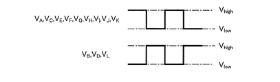
- FIG. 13A is an example of a waveform diagram of signals V A to V L supplied to each electrode in order to place the switch liquid crystal panel 20 in the barrier lighting state of FIG.
- the control unit 40 drives some of the electrodes included in one of the electrode groups selected from the first electrode group 211 and the second electrode group 221 in the first phase, and the other electrodes have the opposite polarity to the first phase. Drive in the second phase.
- the electrode driven in the first phase is schematically shown with a sand pattern. The same applies to FIGS. 14, 16A, and 16B described later.
- the controller 40 includes the electrodes 211B, 211D, and 211L included in the first electrode group 211 in the first phase, and the other electrodes (electrodes 211F, 211H, 211J, and electrodes 221A to 221K) as the second phase.
- a rectangular AC voltage having a phase is applied.
- the amplitudes of the signals V A to V L are all equal.
- the signals V A to V L are either a predetermined high level potential (V high , for example, 5 V) or a predetermined low level potential (V low , for example, 0 V).
- the switch liquid crystal panel 20 is a normally white liquid crystal. Therefore, the barrier BR is formed in a portion where the electrode 221A and the electrode 211B overlap in plan view (xy plan view).
- a barrier BR is formed in a portion where the electrode 211B, the electrode 221C, the electrode 221C, the electrode 211D, the electrode 211D, the electrode 221E, the electrode 221K, the electrode 211L, and the electrode 211L, the electrode 221A overlap in plan view. Is done.
- the switch liquid crystal panel 20 is a normally white liquid crystal. Therefore, the slit SL is formed in a portion where the electrode 221E and the electrode 211F overlap in plan view.
- a slit SL is formed at a portion where the electrode 211F and the electrode 221G, the electrode 221G and the electrode 211H, the electrode 211H and the electrode 221I, the electrode 221I and the electrode 211J, and the electrode 211J and the electrode 221K overlap in plan view. Is done.
- a barrier BR is formed in a portion that overlaps the electrodes 211B, 211D, and 211L driven in the first phase in a plan view
- a slit SL is formed in a portion that overlaps the electrodes 211F, 211H, and 211J in a plan view.
- FIG. 13B is another example of a waveform diagram of signals V A to V L supplied to each electrode in order to place the switch liquid crystal panel 20 in the barrier lighting state of FIG.
- the control unit 40 sets the electrodes 211B, 211D, and 211L included in the first electrode group 211 to a constant potential V 0 (for example, GND), and other electrodes (the electrodes 211F, 211H, 211J, and the electrode 221A).
- V 0 for example, GND
- other electrodes the electrodes 211F, 211H, 211J, and the electrode 221A.
- V a 5 V
- is generated in a portion overlapping the electrodes 211B, 211D, and 211L in plan view, and a barrier BR is formed.
- a potential difference does not occur in a portion overlapping the electrodes 211F, 211H, and 211J in plan view, so that a slit SL is formed.
- FIG. 13C is still another example of a waveform diagram of signals V A to V L supplied to each electrode in order to bring the switch liquid crystal panel 20 into the barrier lighting state of FIG.
- V a 5 V
- is generated in a portion overlapping the electrodes 211B, 211D, and 211L in plan view, and a barrier BR is formed.
- a potential difference does not occur in a portion overlapping the electrodes 211F, 211H, and 211J in plan view, so that a slit SL is formed.
- FIG. 14 is a cross-sectional view schematically showing another one of the barrier lighting states of the switch liquid crystal panel 20.
- 15A to 15C are examples of waveform diagrams of signals V A to V L supplied to the respective electrodes in order to set the switch liquid crystal panel 20 to the barrier lighting state of FIG.
- the description of FIGS. 15A to 15C is the same as FIGS. 13A to 13C, and will not be repeated.
- the barrier lighting state can be controlled with half of the electrode interval BP as a minimum unit.
- the characteristics of the switch liquid crystal panel 20 differ depending on the refractive index anisotropy ⁇ n. Specifically, crosstalk can be reduced as ⁇ n is smaller.
- FIG. 16A is a cross-sectional view schematically showing one of the barrier lighting states of the switch liquid crystal panel 20 when the refractive index anisotropy ⁇ n of the liquid crystal molecules is large.
- the electrode 221E, the electrode 221G, and the electrode 221I are driven in the first phase.
- an electric field parallel to the z direction is formed in a portion overlapping the electrodes 221E, 221G, and 221I in plan view.
- the electric field is not parallel to the z direction and has an in-plane direction component. This disturbs the alignment of the liquid crystal molecules. This disorder of orientation is greatest at the substrate interface of the liquid crystal layer, and the closer to the middle part of the liquid crystal layer, the closer the orientation is to the normal orientation as on the electrode.
- FIG. 16B is a cross-sectional view schematically showing one of the barrier lighting states of the switch liquid crystal panel 20 when the refractive index anisotropy ⁇ n of the liquid crystal molecules is small.
- the refractive index anisotropy ⁇ n of the liquid crystal molecules is small, the residual retardation ⁇ n ⁇ d due to the liquid crystal molecules not normally aligned near the substrate interface becomes relatively small. For this reason, a decrease in the light shielding property of the barrier region is suppressed.
- a preferable ⁇ n is 0.14 or less.
- the retardation ⁇ n ⁇ d in the interelectrode region is about 90 nm.
- the transmittance is 10% or less, and a comparatively good light-shielding property is obtained even in the inter-electrode region.
- the stereoscopic display device 1 according to the first embodiment of the present invention has been described above.
- the example in which the first electrode group 211 includes six types of electrodes has been described. This configuration is an example, and the number of electrodes constituting the first electrode group 211 is arbitrary.
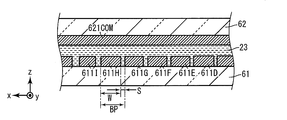
- FIG. 17 is a cross-sectional view showing a schematic configuration of the stereoscopic display device 2 according to the second embodiment of the present invention.
- the stereoscopic display device 2 includes a switch liquid crystal panel 60 instead of the switch liquid crystal panel 20.
- the switch liquid crystal panel 60 includes a first substrate 61 instead of the first substrate 21 of the switch liquid crystal panel 20, and includes a second substrate 62 instead of the second substrate 22.
- electrodes 611A to 611L to which 12 systems of signals V A to V L are supplied are formed on the first substrate 61.
- the electrodes 611A to 611L are periodically formed in the x direction, like the electrodes 211B to 211K of the first substrate 21.
- a common electrode 621 COM is formed so as to cover substantially the entire active area of the second substrate 62.
- the common electrode 621COM, signal V COM is supplied.
- FIG. 18 is a cross-sectional view showing a part of the switch liquid crystal panel 60 in an enlarged manner.
- BP ⁇ / 12 ⁇ PP / 6.
- the switch liquid crystal panel 60 like the switch liquid crystal panel 20, is a twisted nematic liquid crystal and is a normally white liquid crystal.
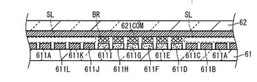
- FIG. 19 is a cross-sectional view schematically showing one of the barrier lighting states of the switch liquid crystal panel 60.
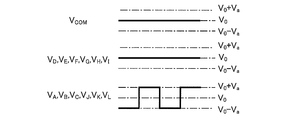
- FIG. 20A is an example of a waveform diagram of signals V COM and V A to V L supplied to each electrode in order to place the switch liquid crystal panel 60 in the barrier lighting state of FIG.
- the control unit 40 drives the common electrode 621COM and the electrodes 611D to 611I with the same phase, and drives the other electrodes with a phase opposite to these.
- the electrode driven with the phase opposite in polarity to the common electrode 621COM is schematically shown with a sand pattern. The same applies to FIGS. 21A and 21B described later.
- control unit 40 applies rectangular AC voltages having opposite polarities to the common electrode 621COM, the electrodes 611D to 611I, and the other electrodes.
- the amplitudes of the signals V COM and V A to V L are all preferably equal.
- the signals V COM and V A to V L are either a predetermined high level potential (V high , for example, 5 V) or a predetermined low level potential (V low , for example, 0 V).
- the switch liquid crystal panel 60 is a normally white liquid crystal. Therefore, the barrier BR is formed in a portion where the common electrode 621COM and the electrode 611A overlap in plan view (xy plan view).
- the common electrode 621COM and the electrode 611B, the common electrode 621COM and the electrode 611C, the common electrode 621COM and the electrode 611J, the common electrode 621COM and the electrode 611K, and the common electrode 621COM and the electrode 611L overlap in a plan view.
- a barrier BR is formed.
- the switch liquid crystal panel 20 is a normally white liquid crystal. Therefore, the slit SL is formed in a portion where the common electrode 621COM and the electrodes 611D to 611I overlap in a plan view.
- the slit SL is formed at a position overlapping with the electrode driven in the same phase as the common electrode 621COM in plan view, and the barrier BR is formed at a position overlapping with other electrodes in plan view.
- FIG. 20B is another example of a waveform diagram of signals V COM and V A to V L supplied to each electrode in order to bring the switch liquid crystal panel 60 into the barrier lighting state of FIG.
- the control unit 40 sets the common electrode 621COM and the electrodes 611D to 611I to a constant potential V 0 (for example, GND), and the electrodes 611A, 611B, 611C, 611J, 611K, and 611L.
- V 0 for example, GND
- is generated in a portion overlapping the electrodes 611A, 611B, 611C, 611J, 611K, and 611L in plan view, and a barrier BR is formed.
- a potential difference does not occur in a portion that overlaps with the electrodes 611D to 611I in plan view, so that a slit SL is formed.
- FIG. 20C is still another example of waveform diagrams of signals V COM and V A to V L supplied to the respective electrodes in order to bring the switch liquid crystal panel 60 into the barrier lighting state of FIG.
- V a half width
- the electrode 611B, the electrode 611C, the electrode 611J, the electrode 611K, and the electrode 611L are set to a constant potential V 0 (for example, GND).
- is generated in a portion overlapping the electrodes 611A, 611B, 611C, 611J, 611K, and 611L in plan view, and a barrier BR is formed.
- a potential difference does not occur in the portion overlapping with the electrodes 611D, 611F, and 611H in plan view, so that a slit SL is formed.
- the barrier lighting state can be controlled in units of the electrodes 611A to 611L.
- the barrier lighting state can be controlled with the electrode interval BP as the minimum unit.
- the characteristics of the switch liquid crystal panel 60 differ depending on the refractive index anisotropy ⁇ n. Specifically, crosstalk can be reduced as ⁇ n is smaller.
- FIG. 21A is a cross-sectional view schematically showing one of the barrier lighting states of the switch liquid crystal panel 60 when the refractive index anisotropy ⁇ n of the liquid crystal molecules is large.
- a signal having a polarity opposite to that of the common electrode 621COM is applied to the electrodes 611D to 211I.
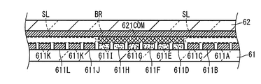
- FIG. 21B is a cross-sectional view schematically showing one of the barrier lighting states of the switch liquid crystal panel 60 when the refractive index anisotropy ⁇ n of the liquid crystal molecules is small.
- the refractive index anisotropy ⁇ n of the liquid crystal molecules is small, the residual retardation ⁇ n ⁇ d due to the liquid crystal molecules not normally aligned near the substrate interface becomes relatively small. For this reason, a decrease in the light shielding property of the barrier region is suppressed.
- a preferable ⁇ n is 0.14 or less.
- the second embodiment of the present invention has been described above.
- an example in which 12 types of electrodes are formed on the first substrate 61 has been described.
- This configuration is an example, and the number of electrodes formed on the first substrate 61 is arbitrary.
- FIG. 22 is a diagram illustrating the angular characteristics of the luminance of the stereoscopic display device when the barrier lighting state is fixed.
- the luminance AL is a luminance observed at an angle ⁇ ⁇ 0 when the right-eye image is displayed in black and the left-eye image is displayed in white.
- Brightness A R in the same screen, a luminance observed at an angle theta> 0.
- the luminance BL is a luminance observed at an angle ⁇ ⁇ 0 when the right-eye image is displayed in white and the left-eye image is displayed in black.
- Luminance B R in the same screen, a luminance observed at an angle theta> 0.
- the luminance CL is a luminance observed at an angle ⁇ ⁇ 0 when both the right-eye image and the left-eye image are displayed in black.
- Luminance C R is the same screen, a luminance observed at an angle theta> 0.
- the left-eye crosstalk XT (L) is defined by the following equation.
- right-eye crosstalk XT (R) is defined by the following equation.
- FIG. 23 is a diagram illustrating angular characteristics of the left-eye crosstalk XT (L) and the right-eye crosstalk XT (R).
- Left-eye crosstalk XT (L) takes a minimum value at the angle - [theta] 0, increases as deviated from the angle - [theta] 0.
- the right-eye crosstalk XT (R) is at an angle + theta 0 takes a minimum value, increases as deviated from the angle + theta 0.
- the minimum value of XT (R) and XT (L) is defined as crosstalk XT.
- a stereoscopic display device according to the configuration of the stereoscopic display device 1 according to the first embodiment (FIGS. 7 and 8) was produced.
- the electrode pitch PP 53.7 ⁇ m
- the barrier pitch BP 17.89 ⁇ m
- the electrode width W 13.89 ⁇ m
- the gap S between the electrodes S 4 ⁇ m.
- FIG. 25 is a graph showing the relationship between the refractive index anisotropy ⁇ n and the crosstalk XT. As shown in FIG. 25, it was confirmed that the crosstalk XT depends on the refractive index anisotropy ⁇ n, and the crosstalk XT tends to decrease as the refractive index anisotropy ⁇ n decreases.
- one criterion is to reduce the crosstalk XT to 1.5% or less. From FIG. 25, it was found that if the refractive index anisotropy ⁇ n is 0.14 or less, the crosstalk XT can be 1.5% or less.
- followability is an indicator of how the 3D display looks when the barrier is moved according to the position of the observer's head while actually tracking, while varying the frame rate of the camera used as a position sensor, Changes in brightness and changes in crosstalk were evaluated visually.
- the frame rate of the camera is 60 fps
- the case where the change in luminance and the change in crosstalk cannot be confirmed is “ ⁇ ”
- the case where the change cannot be confirmed at 60 to 120 fps is indicated as“ ⁇ ”.
- “ ⁇ ” is indicated when a slight luminance change or crosstalk change is visible at 120 fps
- “X” is indicated when the luminance change and crosstalk change are large even at 120 fps.
- the crosstalk XT exceeded 1.5%. This is probably because the refractive index anisotropy ⁇ n was high.
- the three-dimensional display device 3 had a crosstalk XT of 1.5% or less and good followability. Also, 1st-min. Since the setting was satisfied, the transmittance in the two-dimensional display mode was high.
- the 3D display device 4 had a low crosstalk XT, the followability was slightly inferior. This is presumably because the cell thickness d was slightly thick.
- the 3D display device 5 had low crosstalk XT, the followability was poor. This is presumably because the cell thickness d was thick.
- the stereoscopic display device of No. 6 had a crosstalk XT of 1.5% or less and good followability. However, 1st-min. Since it was out of the setting, the transmittance in the two-dimensional display mode was low.
- a stereoscopic display device according to the configuration of the stereoscopic display device 2 according to the second embodiment (FIGS. 17 and 18) was produced.
- the electrode pitch PP 53.7 ⁇ m
- the barrier pitch BP 8.95 ⁇ m
- the electrode width W 4.95 ⁇ m
- the gap S between the electrodes S 4 ⁇ m.
- the example in which the display panel 10 and the switch liquid crystal panel 20 are arranged so that the switch liquid crystal panel 20 is on the viewer 90 side has been described.
- the display panel 10 and the switch liquid crystal panel 20 may be overlapped so that the display panel 10 is on the viewer 90 side.
- the light separated by the switch liquid crystal panel 20 passes through the display panel 10.
- the light separated by the switch liquid crystal panel 20 is scattered or diffracted by the display panel 10.
- the crosstalk is worse than the configuration in which the switch liquid crystal panel 20 is arranged closer to the viewer 90 than the display panel 10, but the luminance angle change becomes gentle.
- the switch liquid crystal panel 20 is arranged on the viewer side, the light from the display panel 10 is separated by the switch liquid crystal panel 20. This configuration is superior in separation characteristics as compared with the configuration in which the display panel 10 is disposed on the viewer side.
- liquid crystal display panel is used as the display panel 10
- an organic EL (ElectroLuminescence) panel may be used.
- MEMS Micro Electric Mechanical System
- plasma display panel may be used.
- the present invention can be used industrially as a stereoscopic display device.
Landscapes
- Physics & Mathematics (AREA)
- Multimedia (AREA)
- Signal Processing (AREA)
- Engineering & Computer Science (AREA)
- Nonlinear Science (AREA)
- General Physics & Mathematics (AREA)
- Optics & Photonics (AREA)
- Chemical & Material Sciences (AREA)
- Crystallography & Structural Chemistry (AREA)
- Mathematical Physics (AREA)
- Geometry (AREA)
- Liquid Crystal (AREA)
- Testing, Inspecting, Measuring Of Stereoscopic Televisions And Televisions (AREA)
- Devices For Indicating Variable Information By Combining Individual Elements (AREA)
Abstract
Description
以下、図面を参照し、本発明の実施の形態を詳しく説明する。図中同一または相当部分には同一符号を付してその説明は繰り返さない。なお、説明を分かりやすくするために、以下で参照する図面においては、構成が簡略化または模式化して示されたり、一部の構成部材が省略されたりしている。また、各図に示された構成部材間の寸法比は、必ずしも実際の寸法比を示すものではない。
[全体の構成]
図1は、本発明の第1の実施形態にかかる立体表示装置1の構成を示す模式的断面図である。立体表示装置1は、表示パネル10と、スイッチ液晶パネル20と、接着樹脂30と備えている。表示パネル10とスイッチ液晶パネル20とは、スイッチ液晶パネル20が観察者90側になるように重ねて配置され、接着樹脂30によって貼り合わされている。
図6Aは、スイッチ液晶パネル20の第1基板21の構成を示す平面図である。第1基板21には、第1電極群211が形成されている。第1電極群211は、x方向に沿って電極間隔BPで配置された複数の電極を含んでいる。複数の電極のそれぞれは、y方向に延びて、互いに平行に配置されている。
Δn・d=(m2-(Φ/π)2)1/2・λ
図12は、スイッチ液晶パネル20のバリア点灯状態の一つを模式的に示す断面図である。図13Aは、スイッチ液晶パネル20を図12のバリア点灯状態にするために各電極に供給する信号VA~VLの波形図の一例である。
図17は、本発明の第2の実施形態にかかる立体表示装置2の概略構成を示す断面図である。立体表示装置2は、スイッチ液晶パネル20に代えてスイッチ液晶パネル60を備えている。
次に、図19および図20A~図20Cを参照して、スイッチ液晶パネル60の駆動方法を説明する。
以下、本発明にかかる立体表示装置のより具体的な構成例を説明する。この構成例は、本発明を限定するものではない。


第1の実施形態にかかる立体表示装置1の構成(図7、図8)に準じた立体表示装置を作製した。なお、電極ピッチPP=53.7μm、バリアピッチBP=17.89μm、電極の幅W=13.89μm、電極間の隙間S=4μmとした。バリア移動ピッチはBP/2=8.95μmである。
第2の実施形態にかかる立体表示装置2の構成(図17、図18)に準じた立体表示装置を作製した。なお、電極ピッチPP=53.7μm、バリアピッチBP=8.95μm、電極の幅W=4.95μm、電極間の隙間S=4μmとした。バリア移動ピッチは、BP=8.95μmである。
以上、本発明についての実施形態を説明したが、本発明は上述の各実施形態のみに限定されず、発明の範囲内で種々の変更が可能である。また、各実施形態は、適宜組み合わせて実施することが可能である。
Claims (10)
- 画像を表示する表示パネルと、
前記表示パネルに重ねて配置されるスイッチ液晶パネルと、
観察者の位置情報を取得する位置センサと、
所定の整列方向に沿って透過領域と非透過領域とが周期的に形成された視差バリアを、前記位置情報に応じて前記整列方向に沿って移動させて前記スイッチ液晶パネルに表示させる制御部とを備え、
前記スイッチ液晶パネルは、
液晶分子の屈折率異方性Δnが0.14以下である液晶層と、
前記液晶層を挟んで対向する第1基板および第2基板と、
前記第1基板および前記第2基板の少なくとも一方に形成され、前記整列方向に沿って配置された複数の電極を含む電極群とを含む、立体表示装置。 - 前記スイッチ液晶パネルは、ノーマリーホワイトである、請求項1に記載の立体表示装置。
- 前記液晶層のリタデーションは、ファーストミニマムに設定されている、請求項1または2に記載の立体表示装置。
- 前記液晶層の厚さは、5.5μm以下である、請求項1~3のいずれか一項に記載の立体表示装置。
- 前記液晶層に電圧が印加されていないとき、前記第1基板側の液晶分子の配向方向と、前記第2基板側の液晶分子の配向方向とが、互いに90°異なる、請求項1~4のいずれか一項に記載の立体表示装置。
- 前記電極群は、
前記第1基板に形成され、前記整列方向に沿って所定間隔で配置された複数の電極を含む第1電極群と、
前記第2基板に形成され、前記整列方向に沿って前記所定間隔で配置された複数の電極を含む第2電極群とを含み、
前記第1電極群と前記第2電極群とは、前記整列方向において互いに前記所定間隔の半分だけずれて配置される、請求項1~5のいずれか一項に記載の立体表示装置。 - 前記電極群は、
前記第1基板に形成され、前記整列方向に沿って所定間隔で配置された複数の電極を含む第1電極群と、
前記第2基板の概略全面に形成される共通電極とを含む、請求項1~5に記載の立体表示装置。 - 前記スイッチ液晶パネルは、前記表示パネルよりも前記観察者側に配置される、請求項1~7のいずれか一項に記載の立体表示装置。
- 前記表示パネルは、前記スイッチ液晶パネルよりも前記観察者側に配置される、請求項1~7のいずれか一項に記載の立体表示装置。
- 前記表示パネルは、液晶表示パネルである、請求項1~9のいずれか一項に記載の立体表示装置。
Priority Applications (3)
| Application Number | Priority Date | Filing Date | Title |
|---|---|---|---|
| JP2015540420A JP6125027B2 (ja) | 2013-10-01 | 2014-08-20 | 立体表示装置 |
| US15/026,301 US9784982B2 (en) | 2013-10-01 | 2014-08-20 | Stereoscopic display device |
| CN201480054104.9A CN105593748B (zh) | 2013-10-01 | 2014-08-20 | 立体显示装置 |
Applications Claiming Priority (2)
| Application Number | Priority Date | Filing Date | Title |
|---|---|---|---|
| JP2013206650 | 2013-10-01 | ||
| JP2013-206650 | 2013-10-01 |
Publications (1)
| Publication Number | Publication Date |
|---|---|
| WO2015049929A1 true WO2015049929A1 (ja) | 2015-04-09 |
Family
ID=52778525
Family Applications (1)
| Application Number | Title | Priority Date | Filing Date |
|---|---|---|---|
| PCT/JP2014/071777 Ceased WO2015049929A1 (ja) | 2013-10-01 | 2014-08-20 | 立体表示装置 |
Country Status (4)
| Country | Link |
|---|---|
| US (1) | US9784982B2 (ja) |
| JP (1) | JP6125027B2 (ja) |
| CN (1) | CN105593748B (ja) |
| WO (1) | WO2015049929A1 (ja) |
Cited By (2)
| Publication number | Priority date | Publication date | Assignee | Title |
|---|---|---|---|---|
| JP2019148621A (ja) * | 2018-02-26 | 2019-09-05 | 三菱電機株式会社 | 表示装置、および、表示装置の駆動方法 |
| JP2021021951A (ja) * | 2015-11-09 | 2021-02-18 | ソニー株式会社 | 表示装置 |
Families Citing this family (3)
| Publication number | Priority date | Publication date | Assignee | Title |
|---|---|---|---|---|
| CN104104934B (zh) * | 2012-10-04 | 2019-02-19 | 陈笛 | 无眼镜多观众三维显示的组件与方法 |
| US9872013B2 (en) * | 2013-10-25 | 2018-01-16 | Sharp Kabushiki Kaisha | Stereoscopic display device |
| KR102436564B1 (ko) * | 2017-12-29 | 2022-08-26 | 엘지디스플레이 주식회사 | 배리어 패널을 포함하는 입체 영상 표시 장치 |
Citations (5)
| Publication number | Priority date | Publication date | Assignee | Title |
|---|---|---|---|---|
| JPH07287196A (ja) * | 1994-02-25 | 1995-10-31 | Sanyo Electric Co Ltd | 立体表示装置 |
| JPH0876139A (ja) * | 1994-07-07 | 1996-03-22 | Sanyo Electric Co Ltd | 液晶表示装置 |
| JPH11352454A (ja) * | 1998-06-11 | 1999-12-24 | Asahi Glass Co Ltd | アレイシート、その製造方法、3次元表示装置および3次元像表示システム |
| WO2012035806A1 (ja) * | 2010-09-13 | 2012-03-22 | 株式会社有沢製作所 | 立体画像表示装置 |
| JP2013024957A (ja) * | 2011-07-19 | 2013-02-04 | Mitsubishi Electric Corp | 表示装置 |
Family Cites Families (4)
| Publication number | Priority date | Publication date | Assignee | Title |
|---|---|---|---|---|
| JP3852935B2 (ja) * | 2003-05-30 | 2006-12-06 | 株式会社東芝 | 立体画像表示装置 |
| WO2013061458A1 (ja) * | 2011-10-28 | 2013-05-02 | 株式会社東芝 | 画像表示装置 |
| KR20130106217A (ko) * | 2012-03-19 | 2013-09-27 | 삼성디스플레이 주식회사 | 3차원 영상 표시 방법 및 이를 수행하기 위한 표시 장치 |
| US9677003B2 (en) * | 2012-03-30 | 2017-06-13 | Dic Corporation | Liquid crystal display device and method for producing the same |
-
2014
- 2014-08-20 CN CN201480054104.9A patent/CN105593748B/zh active Active
- 2014-08-20 US US15/026,301 patent/US9784982B2/en not_active Expired - Fee Related
- 2014-08-20 WO PCT/JP2014/071777 patent/WO2015049929A1/ja not_active Ceased
- 2014-08-20 JP JP2015540420A patent/JP6125027B2/ja not_active Expired - Fee Related
Patent Citations (5)
| Publication number | Priority date | Publication date | Assignee | Title |
|---|---|---|---|---|
| JPH07287196A (ja) * | 1994-02-25 | 1995-10-31 | Sanyo Electric Co Ltd | 立体表示装置 |
| JPH0876139A (ja) * | 1994-07-07 | 1996-03-22 | Sanyo Electric Co Ltd | 液晶表示装置 |
| JPH11352454A (ja) * | 1998-06-11 | 1999-12-24 | Asahi Glass Co Ltd | アレイシート、その製造方法、3次元表示装置および3次元像表示システム |
| WO2012035806A1 (ja) * | 2010-09-13 | 2012-03-22 | 株式会社有沢製作所 | 立体画像表示装置 |
| JP2013024957A (ja) * | 2011-07-19 | 2013-02-04 | Mitsubishi Electric Corp | 表示装置 |
Cited By (3)
| Publication number | Priority date | Publication date | Assignee | Title |
|---|---|---|---|---|
| JP2021021951A (ja) * | 2015-11-09 | 2021-02-18 | ソニー株式会社 | 表示装置 |
| JP7026186B2 (ja) | 2015-11-09 | 2022-02-25 | ソニーグループ株式会社 | 表示装置、表示ユニット、および透明板ユニット |
| JP2019148621A (ja) * | 2018-02-26 | 2019-09-05 | 三菱電機株式会社 | 表示装置、および、表示装置の駆動方法 |
Also Published As
| Publication number | Publication date |
|---|---|
| CN105593748B (zh) | 2018-12-28 |
| CN105593748A (zh) | 2016-05-18 |
| US20160223827A1 (en) | 2016-08-04 |
| JP6125027B2 (ja) | 2017-05-10 |
| JPWO2015049929A1 (ja) | 2017-03-09 |
| US9784982B2 (en) | 2017-10-10 |
Similar Documents
| Publication | Publication Date | Title |
|---|---|---|
| JP5969699B2 (ja) | 立体表示装置 | |
| US9063382B2 (en) | Barrier panel and three dimensional image display device using the same | |
| CN105190409B (zh) | 立体显示装置 | |
| US9497444B2 (en) | Stereoscopic display device | |
| US20170045763A1 (en) | Stereoscopic display device | |
| CN105683814B (zh) | 立体显示装置 | |
| JP6009648B2 (ja) | 立体表示装置 | |
| JP6125027B2 (ja) | 立体表示装置 | |
| JP6100390B2 (ja) | 立体表示装置 | |
| CN105683823B (zh) | 立体显示装置 | |
| CN102749762A (zh) | 显示装置 | |
| WO2005054930A1 (ja) | 表示パネルおよび表示装置 | |
| US9983445B2 (en) | Liquid crystal lens panel and display device including liquid crystal lens panel | |
| JP5669945B2 (ja) | 立体表示装置 | |
| WO2017122595A1 (ja) | 表示装置、液晶パネルの駆動方法 |
Legal Events
| Date | Code | Title | Description |
|---|---|---|---|
| 121 | Ep: the epo has been informed by wipo that ep was designated in this application |
Ref document number: 14850382 Country of ref document: EP Kind code of ref document: A1 |
|
| ENP | Entry into the national phase |
Ref document number: 2015540420 Country of ref document: JP Kind code of ref document: A |
|
| WWE | Wipo information: entry into national phase |
Ref document number: 15026301 Country of ref document: US |
|
| NENP | Non-entry into the national phase |
Ref country code: DE |
|
| 122 | Ep: pct application non-entry in european phase |
Ref document number: 14850382 Country of ref document: EP Kind code of ref document: A1 |