WO2015033733A1 - 半導体装置とその製造方法 - Google Patents
半導体装置とその製造方法 Download PDFInfo
- Publication number
- WO2015033733A1 WO2015033733A1 PCT/JP2014/070845 JP2014070845W WO2015033733A1 WO 2015033733 A1 WO2015033733 A1 WO 2015033733A1 JP 2014070845 W JP2014070845 W JP 2014070845W WO 2015033733 A1 WO2015033733 A1 WO 2015033733A1
- Authority
- WO
- WIPO (PCT)
- Prior art keywords
- implantation region
- range
- impurity implantation
- semiconductor substrate
- impurity
- Prior art date
- Legal status (The legal status is an assumption and is not a legal conclusion. Google has not performed a legal analysis and makes no representation as to the accuracy of the status listed.)
- Ceased
Links
Images



Classifications
-
- H—ELECTRICITY
- H10—SEMICONDUCTOR DEVICES; ELECTRIC SOLID-STATE DEVICES NOT OTHERWISE PROVIDED FOR
- H10D—INORGANIC ELECTRIC SEMICONDUCTOR DEVICES
- H10D30/00—Field-effect transistors [FET]
- H10D30/60—Insulated-gate field-effect transistors [IGFET]
-
- H—ELECTRICITY
- H10—SEMICONDUCTOR DEVICES; ELECTRIC SOLID-STATE DEVICES NOT OTHERWISE PROVIDED FOR
- H10D—INORGANIC ELECTRIC SEMICONDUCTOR DEVICES
- H10D64/00—Electrodes of devices having potential barriers
- H10D64/20—Electrodes characterised by their shapes, relative sizes or dispositions
- H10D64/27—Electrodes not carrying the current to be rectified, amplified, oscillated or switched, e.g. gates
- H10D64/311—Gate electrodes for field-effect devices
- H10D64/411—Gate electrodes for field-effect devices for FETs
- H10D64/511—Gate electrodes for field-effect devices for FETs for IGFETs
- H10D64/517—Gate electrodes for field-effect devices for FETs for IGFETs characterised by the conducting layers
- H10D64/519—Gate electrodes for field-effect devices for FETs for IGFETs characterised by the conducting layers characterised by their top-view geometrical layouts
Definitions
- a stacked structure of a gate insulating film and a gate electrode is formed on a part of the surface of a semiconductor substrate, and an impurity implantation region is formed in a semiconductor substrate in a range adjacent to the stacked structure.
- a semiconductor device in which an inversion layer is formed on a semiconductor substrate in a range facing a gate electrode through a gate insulating film by a voltage applied to the semiconductor device and a manufacturing method thereof are disclosed.
- a laminated structure 8 of a gate insulating film 4 and a gate electrode 6 is formed on a part of the surface 2a of the semiconductor substrate 2, and a first range adjacent to the laminated structure 8 is formed.
- a semiconductor structure in which a first impurity implantation region 10 is formed in a semiconductor substrate 2 and a second impurity implantation region 12 is formed in a second range of the semiconductor substrate 2 adjacent to the stacked structure 8 is known.
- the conductivity type of the first impurity implantation region 10 and the conductivity type of the second impurity implantation region 12 are different from the conductivity type of the semiconductor substrate 2 in the range facing the gate electrode 6 through the gate insulating film 4.
- Adjusted to A voltage applied to the gate electrode 6 can control whether or not an inversion layer is formed on the semiconductor substrate 2 in a range facing the gate electrode 6 through the gate insulating film 4.
- the resistance between the second impurity implantation regions 12 can be controlled.
- FIG. 8 (2) shows a cross section of the semiconductor device after the heat treatment, and a thermal oxide film 16 is formed on the upper surface and side surfaces of the laminated structure 8.
- the gate electrode 6 in a range along the interface between the gate insulating film 4 and the gate electrode 6 is oxidized.
- the semiconductor substrate 2 in a range along the interface between the gate insulating film 4 and the semiconductor substrate 2 is also oxidized.
- the thickness of the thermal oxide film 14 separating the gate electrode 6 and the semiconductor substrate 2 increases. Since the oxidation along the interface proceeds as shown by the arrow a, the thickness of the thermal oxide film 14 that separates the gate electrode 6 and the semiconductor substrate 2 increases as the thickness approaches the contour 8a of the stacked structure 8.
- Reference numeral 5 indicates a range in which the thermal oxide film is thickened as described above, and is referred to as a bird's beak.
- the inner contour 10a of the first impurity implantation region 10 and the inner contour 12a of the second impurity implantation region 12 are more than the contour 8a of the stacked structure 8. Enter the inside by a distance A.
- the bird's beak 5 extends inward from the contour 8 a of the laminated structure 8.
- the bird's beak 5 enters inside the distance 8 from the outline 8 a of the laminated structure 8.
- Reference numeral 5 a indicates the tip position of the bird's beak 5 (the position extending inward most). Usually, distance A ⁇ distance B.
- FIG. 8B illustrates a case where the inversion layer is formed only in a range where the bird's beak 5 is not formed, and the formation range of the inversion layer is indicated by reference numeral 20.
- the common reference number 20 is used. The same reference numbers are used for regions and region formation ranges.
- a range 22 corresponding to the distance C is a low impurity concentration range where no impurity is implanted unless an inversion layer is formed (usually, if the gate insulating film is thin, a voltage is applied to the gate electrode 6. The concentration is adjusted to such a low level that an inversion layer is formed).
- the range 22 of the distance C is a high resistance region.
- Patent Document 1 describes a technique for avoiding the occurrence of a phenomenon in which the thickness of the thermal oxide film 14 separating the gate electrode 6 and the semiconductor substrate 2 increases in the range along the outline 8a of the stacked structure 8 when the thermal oxide film 16 is formed. ing.
- a thermal oxide film is formed after forming a nitride film on the side surface of the laminated structure 8 of the gate insulating film 4 and the gate electrode 6.
- the side surface of the gate electrode 6 is insulated by a nitride film
- the upper surface of the gate electrode 6 is insulated by a thermal oxide film.
- Patent Document 1 it is possible to prevent the thickness of the thermal oxide film 14 separating the gate electrode 6 and the semiconductor substrate 2 from increasing in a range along the outline 8 a of the stacked structure 8, and a voltage is applied to the gate electrode 6. Even if the inversion layer is formed, the problem that the resistance between the first impurity implantation region 10 and the second impurity implantation region 12 does not decrease can be solved.
- the technique described in Patent Document 1 requires a nitride film forming step. In the normal MOS manufacturing process, the nitride film forming process is not performed.
- the technique of Patent Document 1 requires a nitride film forming step and an etching step that are not normally required, and the process cost increases.
- a technique for preventing the phenomenon that the impurity implantation region and the inversion layer are separated in the range along the outline 8a of the stacked structure 8 without forming a nitride film is disclosed.
- FIG. 9 shows a cross-sectional structure of the LDD.
- the same reference numerals are used for ranges corresponding to FIG.
- impurities are implanted using the stacked structure 8 as a mask to form a first impurity low concentration implantation region 10b and a second impurity low concentration implantation region 12b.
- a thermal oxide film 16 is formed around the laminated structure 8.
- impurities are implanted using the thermal oxide film 16 as a mask to form a first impurity high concentration implantation region 10c and a second impurity high concentration implantation region 12c.
- the thickness of the thermal oxide film 14 separating the gate electrode 6 and the semiconductor substrate 2 increases in the range along the outline 8a of the stacked structure 8, and a voltage is applied to the gate electrode 6 to form an inversion layer.
- the resistance between the first impurity low concentration implantation region 10b and the second impurity low concentration implantation region 12b does not decrease.
- FIG. 10 shows a cross-sectional structure of a vertical LDD.
- impurities are implanted using the stacked structure 8 as a mask, and the left first impurity low concentration implantation region 10b1 and the right first impurity low concentration are implanted in a range adjacent to the stacked structure 8.
- An implantation region 10b2 is manufactured. Further, impurities are implanted using the thermal oxide film 16 as a mask, and the left first impurity high concentration implantation region 10c1 and the right first impurity high concentration implantation region 10c2 are manufactured in a region adjacent to the thermal oxide film 16.
- a second impurity low-concentration implantation region 12b is formed in a range extending in the longitudinal direction in the central portion of the semiconductor substrate 2, and a second impurity high-concentration implantation region 12c is formed in a range facing the back surface of the semiconductor substrate 2.
- the conductivity types of the first impurity low concentration implantation regions 10b1 and 10b2, the first impurity high concentration implantation regions 10c1 and 10c2, the second impurity low concentration implantation region 12b, and the second impurity high concentration implantation region 12c are the same. Only the range of the remaining semiconductor substrate 2 is of the opposite conductivity type.
- the thickness of the thermal oxide film 14 separating the gate electrode 6 and the semiconductor substrate 2 increases in the range along the outline 8a of the stacked structure 8, and a voltage is applied to the gate electrode 6 to form an inversion layer. Even if formed, there arises a problem that the resistance between the first impurity low concentration implantation regions 10b1 and 10b2 and the second impurity low concentration implantation region 12b does not decrease.
- a gate insulating film formed on part of the surface of a semiconductor substrate, a gate electrode stacked on the gate insulating film, and a stacked structure of the gate insulating film and the gate electrode are provided.
- a thermal oxide film to be covered and an impurity implantation region formed in a semiconductor substrate in a range adjacent to the stacked structure are provided.
- irregularities are formed in the outline of the opposed range that extends along the outline of the impurity implantation region. .
- FIG. 11 illustrates a state in which the semiconductor substrate 2 is viewed in plan.
- Solid lines 8 b and 8 c show a part of the outline of the range where the stacked structure 8 of the gate insulating film 4 and the gate electrode 6 faces the semiconductor substrate 2.
- the shape of the upper surface and the lower surface of the laminated structure 8 may not match.
- impurities may be implanted obliquely, and the shape of the lower surface (the surface facing or in contact with the semiconductor substrate 2) of the stacked structure 8 is important.
- the solid line 8b indicates the contour of the range in which the contour of the facing range of the stacked structure 8 extends along the contour of the impurity implantation region
- the solid line 8c indicates the contour of the facing range of the stacked structure 8 regardless of the contour of the impurity implanted region.
- the outline of the range is shown.
- the outline of the opposing range of the laminated structure 8 may be referred to as the outline of the laminated structure 8.
- a broken line 12a indicates a part of the outline of the impurity implantation region 12 formed by implanting impurities into the semiconductor substrate 2 using the stacked structure 8 as a mask.
- the impurity is implanted obliquely and the implanted impurity is diffused, and the outline 12a of the impurity-implanted region 12 is located at a position where the distance A has entered from the outline 8b of the stacked structure 8 inward. It is formed.
- the distance A is the distance described with reference to FIG.
- the impurity implantation region 12 is formed in a part of a range adjacent to the stacked structure 8. In the outline of the stacked structure 8, there are a range 8 b extending along the outline 12 a of the impurity implantation region 12 and a range 8 c extending regardless of the contour 12 a of the impurity implantation region 12.
- a chain line 5a in FIG. 11 (1) indicates the outline of the formation range of the bird's beak 5 described in FIG.
- the contour 5a of the bird's beak formation range is located at a distance B from the contour 8b of the laminated structure 8 inward as described above.
- the distance B is the distance described in FIG. 8, and A ⁇ B.
- the outline of the bird's beak formation area and the tip position of the bird's beak are displayed at the same position. In this specification, the same reference number 5a is used for these.
- the high resistance range (range 22 shown by the distance C) is the width of the gate electrode. It extends in the direction (Y direction in the figure).
- a high resistance range 22 is formed across the entire width of the impurity implantation region 12. That is, the inversion layer 20 and the impurity implantation region 12 formed by applying a voltage to the gate electrode are divided by the high resistance range 22 over the entire width of the impurity implantation region 12. A position where the inversion layer 20 is in contact with the impurity implantation region 12 is not formed.
- FIG. 2 shows a case where irregularities are formed in a part 8b of the outline of the laminated structure 8.
- FIG. That is, a case is shown in which the concave portions 8d and the convex portions 8e are alternately and repeatedly formed on the contour 8b in a range extending along the contour 12a of the impurity implantation region 12.
- the contour 8c of the stacked structure 8 extending in a range that is independent of the contour 12a of the impurity implantation region 12 may or may not be uneven.
- a broken line 12a shows a part of the outline of the impurity implantation region 12 formed by implanting impurities into the semiconductor substrate 2 using the laminated structure 8 as a mask.
- the influence of the oblique implantation of the impurities and the diffusion of the implanted impurities influences the contour 12a of the impurity implantation region 12 to be formed at a position that penetrates from the contours 8b and 8c of the stacked structure 8 by the distance A. .
- the distance A is the distance described with reference to FIGS.
- the unevenness is also formed in the contour 12a.
- a dashed-dotted line 5a in FIG. 2 (1) indicates the outline of the formation range of the bird's beak 5 described in FIG.
- the bird's beak 5 is formed by oxidation. Therefore, the bird's beak 5 develops well at a position where oxygen is often supplied, and the bird's beak 5 hardly develops at a position where oxygen is hardly supplied.
- oxygen is often supplied, so the bird's beak 5 penetrates deeply.
- the contour 5a of the bird's beak formation range is located at a distance B from the contour 8e of the laminated structure 8 inward. The distance B is the distance described in FIG. 8, and A ⁇ B.
- the bird's beak 5 hardly develops in the recess 8d.
- FIG. 2 for simplification, the case where the bird's beak 5 does not develop in the recess 8d is illustrated. If the bird's beak 5 is not formed, the outline 5a of the bird's beak formation area coincides with the outline 8d of the laminated structure 8.
- the bird's beak penetration distance changes in the contour 8g in the range connecting the convex portion 8e and the concave portion 8d. Oxygen is often supplied in the portion close to the convex portion 8e, and the bird's beak penetrates deeply. Oxygen is difficult to be supplied in the portion close to the recess 8d, and the bird's beak penetration depth is reduced.
- a hatched range 18 indicates a range in which the impurity implantation region 12 extends beyond the formation range of the bird's beak 5. That is, it shows a range where the impurity implantation region 12 and the inversion layer formation range 20 overlap. Since the bird's beak 5 does not develop in the recess 8d, a region 18 in which the impurity implanted region 12 extends beyond the bird's beak 5 formation range is obtained. When a range 18 in which the impurity implantation region 12 and the inversion layer formation range 20 overlap is obtained, a relationship in which the impurity implantation region 12 and the inversion layer 20 are in direct contact is obtained.
- FIG. 2E shows an EE cross section of FIG. Since no bird's beak is formed in the recess 8 d, the thin gate oxide film 4 reaches the impurity implantation region 12.
- FIG. 2 is schematic, and when viewed in detail, it may differ from the actual formation range. For example, although the case where the bird's beak is not formed in the recess 8d is illustrated, the bird's beak may be formed also in the recess 8d.
- the bird's beak formed by the recess 8d does not grow so much, and the relationship of A> B is established. If the relationship of A> B is obtained, a range where the impurity implantation region and the inversion layer formation range overlap can be obtained. The problem that the resistance between the impurity implantation region and the inversion layer does not decrease is solved.
- the technique of providing irregularities in the outline of the stacked structure is effective for the vertical semiconductor device illustrated in FIG. 10 and also effective for the horizontal semiconductor device illustrated in FIGS.
- a first impurity implantation region is formed in a first range adjacent to the stacked structure of the gate insulating film and the gate electrode, and a second impurity is formed in the second range adjacent to the stacked structure.
- An implantation region is formed.
- the conductivity type of the first impurity implantation region and the conductivity type of the second impurity implantation region are the same, and are different from the conductivity type of the semiconductor substrate in the range facing the gate electrode through the gate insulating film.
- the first impurity implantation region and the second impurity implantation region have a high concentration in the case illustrated in FIG. 8, and a low concentration in the case illustrated in FIG.
- the impurity concentration of the first impurity implantation region and the second impurity implantation region is not limited.
- the first impurity implantation region and the inversion layer are in direct contact, and the second impurity implantation region and the inversion layer are in direct contact.
- the inversion layer By forming the inversion layer, a phenomenon in which the resistance between the first impurity implantation region and the second impurity implantation region is significantly reduced can be obtained.
- the impurity injection region and the bird's beak are formed inside the outline defining the area where the laminated structure and the semiconductor substrate face each other.
- a range is formed, and a range in which the impurity implantation region extends beyond the bird's beak formation range is formed.
- a method for manufacturing a semiconductor device disclosed in this specification includes a step of forming a stacked structure of a gate insulating film and a gate electrode on a part of a surface of a semiconductor substrate, and a part of the surface of the semiconductor substrate through the stacked structure.
- This manufacturing method is characterized in that an unevenness is formed in the outline of the laminated structure extending along the outline of the impurity implantation region when a range in which the laminated structure and the semiconductor substrate face each other is viewed in plan.
- the thermal oxide film there is no problem that the impurity implantation region and the inversion layer are separated by the bird's beak formed during the formation.
- the relationship between the impurity implantation region and the inversion layer formation range in the case of the first embodiment is shown.
- the relationship between the impurity implantation region and the inversion layer formation range in the case of the second embodiment is shown.
- the top view of the laminated structure of 3rd Example is shown.
- the top view of the laminated structure of 4th Example is shown.
- the top view of the laminated structure of 5th Example is shown.
- the top view of the laminated structure of 6th Example is shown.
- the figure which illustrates the problem in the case of a prior art The figure which illustrates the problem in the case of a prior art.
- the relationship between the impurity implantation region and the inversion layer formation range in the case of the conventional technique is shown.
- the gate insulating film is SiO 2 and the gate electrode is polysilicon.
- the semiconductor substrate is a single crystal of Si or SiC.
- FIG. 1 shows a laminated structure 8 of a gate insulating film 4 and a gate electrode 6 of the embodiment.
- the contour 8b of the stacked structure 8 is a contour of a range extending along the impurity implantation region
- the contour 8c is a contour of a range extending regardless of the impurity implantation region. That is, when impurities are implanted into the semiconductor substrate 2 using the stacked structure 8 as a mask, the contour 8b is a contour that governs the impurity implantation range, and the contour 8c is not a contour that governs the impurity implantation range.
- the Y direction in which the contour 8b extends is called the gate width direction
- the X direction in which the contour 8c extends is called the gate length direction.
- concave portions 8d and convex portions 8e are formed so as to repeat alternately in the width direction of the gate. It is not necessary to form irregularities on the contour 8c extending in the length direction of the gate. Impurities are implanted into the semiconductor substrate 2 using the laminated structure 8 as a mask. At that time, as shown by an arrow 24, impurities are implanted from various oblique directions.
- FIG. 2 shows a case where the distance in the width direction of the gate of the concave portion 8d is made smaller than the distance in the width direction of the gate of the convex portion 8e.
- a similar phenomenon can be obtained between the impurity implantation region 10 and the inversion layer 20.
- the resistance between the first impurity implantation region 10 and the second impurity implantation region 12 is significantly reduced.
- FIG. 3 shows a case where the distance in the gate width direction of the convex portion 8e is made smaller than the distance in the gate width direction of the concave portion 8d.
- the distance in the gate width direction of the protrusion 8e is less than 2 ⁇ A.
- A is the distance described with reference to FIG.
- the impurity implantation region 12 is formed in the entire range of the protrusion 8e.
- the impurity implantation region 12 is formed in the entire range on the right side of the contour 12a.
- a broken line 5a indicates a bird's beak formation range.
- a buzz beak is formed on the right side of the broken line 5a, but is not formed on the left side of the broken line 5a.
- a hatched range 18 indicates a range in which the impurity implantation region extends beyond the bird's beak formation range. That is, the range in which the impurity implantation region and the inversion layer are in direct contact with each other is shown.
- the distance in the gate width direction of the protrusion 8e is shortened, a relationship in which the impurity implantation region and the inversion layer are in direct contact with each other over the entire width in the gate width direction is obtained. The on-resistance can be further reduced as compared with FIG.
- FIG. 4 shows the laminated structure 8 of the third embodiment.
- the convex portion 8j is formed at the position where the concave portion 8h is formed, and the concave portion 8k is formed at the position where the convex portion 8i is formed.
- the distance in the gate length direction of the gate electrode 6 is equal at any position in the gate width direction.
- the current distribution when a voltage is applied to the gate electrode 6 is homogenized.
- FIG. 5 shows the laminated structure 8 of the fourth embodiment.
- the recess 8m may have a triangular shape. Or as shown in FIG. 6, you may form a recessed part with the combination of a semicircle and a straight line. The recessed part which consists only of a semicircle may be sufficient.
- FIG. 7 shows the laminated structure of the sixth embodiment. What is important in this embodiment is the shape (lower surface shape) in a range where the laminated structure faces the semiconductor substrate, and the upper surface shape of the laminated structure does not have to coincide with the lower surface shape.
- the recess 8p may include a wall surface that is inclined in the gate width direction or a wall surface that is inclined in the gate length direction. Further, the inclined wall surface may or may not reach the upper surface of the laminated structure.
- the outline of the laminated structure referred to in this specification refers to the outline of the lower surface of the laminated structure (the surface facing or in contact with the semiconductor substrate).
Landscapes
- Insulated Gate Type Field-Effect Transistor (AREA)
Abstract
【課題】半導体基板の表面の一部にゲート絶縁膜とゲート電極の積層構造を形成し、積層構造をマスクにして半導体基板の表面の一部に不純物を注入し、積層構造の露出面に熱酸化膜を形成して半導体装置を製造すると、不純物注入領域と反転層の間に高抵抗領域が介在し、オン抵抗を下げられない。 【解決手段】不純物注入領域12に沿って延びる範囲の積層構造の輪郭8bに凹凸を設ける。凹部では熱酸化膜のバーズビークの形成が抑制され、不純物注入領域12と反転層20が直接的に接触する関係が得られる。
Description
本明細書では、半導体基板の表面の一部にゲート絶縁膜とゲート電極の積層構造が形成されており、その積層構造に隣接する範囲の半導体基板に不純物注入領域が形成されており、ゲート電極に印加する電圧によってゲート絶縁膜を介してゲート電極に対向する範囲の半導体基板に反転層が形成される形式の半導体装置と、その製造方法を開示する。
例えば、図8(1)に示すように、半導体基板2の表面2aの一部にゲート絶縁膜4とゲート電極6の積層構造8が形成されており、積層構造8に隣接する第1範囲の半導体基板2に第1不純物注入領域10が形成されており、積層構造8に隣接する第2範囲の半導体基板2に第2不純物注入領域12が形成されている半導体構造が知られている。この構造の場合、第1不純物注入領域10の導電型と第2不純物注入領域12の導電型が、ゲート絶縁膜4を介してゲート電極6に対向する範囲の半導体基板2の導電型から異なる関係に調整される。ゲート電極6に印加する電圧によってゲート絶縁膜4を介してゲート電極6に対向する範囲の半導体基板2に反転層を形成するか形成しないかを制御することができ、第1不純物注入領域10と第2不純物注入領域12の間の抵抗を制御することができる。
実際に使用可能な半導体装置では、ゲート電極6を絶縁膜で覆っておく必要がある。そのために、積層構造8の露出面に熱酸化膜を形成する工程が実施される。図8(2)は、熱処理後の半導体装置の断面を示し、積層構造8の上面と側面に熱酸化膜16が形成されている。
熱酸化膜16を形成する場合、ゲート絶縁膜4とゲート電極6の界面に沿った範囲のゲート電極6が酸化される。また、ゲート絶縁膜4と半導体基板2の界面に沿った範囲の半導体基板2も酸化される。界面に沿って酸化が進行することで、ゲート電極6と半導体基板2を隔てる熱酸化膜14の厚みが増大する。界面に沿った酸化は矢印aに示すように進行することから、ゲート電極6と半導体基板2を隔てる熱酸化膜14の厚みは、積層構造8の輪郭8aに接近するにつれて増大する。参照番号5は、上記のようにして熱酸化膜が厚くなった範囲を示しており、バーズビークといわれる。
バーズビーク5が形成されて熱酸化膜14が厚くなった範囲では、ゲート電極6に電圧を印加しても反転層が形成されない。すると、第1不純物注入領域10と反転層が離れてしまう現象が生じる。あるいは、第2不純物注入領域12と反転層が離れてしまう現象が生じる。
第1不純物注入領域10と第2不純物注入領域12を形成する場合、積層構造8をマスクにして半導体基板2に不純物を注入する。このとき、図8(1)の矢印24に示すように、種々の方向から不純物を注入する方法を採用するができる。斜めに注入する結果、図8(1)に示すように、第1不純物注入領域10の内側の輪郭10aと、第2不純物注入領域12の内側の輪郭12aは、積層構造8の輪郭8aよりも距離Aだけ内側に侵入する。
バーズビーク5は、積層構造8の輪郭8aから内側に延びる。図8の(2)に示すように、バーズビーク5は、積層構造8の輪郭8aより距離Bだけ内側に侵入する。参照番号5aは、バーズビーク5の先端位置(最も内側に延びた位置)を示している。通常は距離A<距離Bである。
バーズビーク5は、積層構造8の輪郭8aから内側に延びる。図8の(2)に示すように、バーズビーク5は、積層構造8の輪郭8aより距離Bだけ内側に侵入する。参照番号5aは、バーズビーク5の先端位置(最も内側に延びた位置)を示している。通常は距離A<距離Bである。
ゲート電極6に電圧を加えた場合、ゲート電極6と半導体基板2を隔てるゲート絶縁膜14の厚みが薄い範囲では反転層が形成されるものの、ゲート絶縁膜14の厚みが増大した範囲では反転層が形成されない。図8(2)では、バーズビーク5が形成されない範囲にのみ反転層が形成される場合を例示しており、反転層の形成範囲を参照番号20で示している。なお本明細書では、反転層自体と反転層形成範囲が同一に図示されることから、共通の参照番号20を用いる。領域と領域形成範囲についても同一の参照番号を用いる。
前記した距離A,Bに関して、A<Bであると、第1不純物注入領域10と反転層20が距離Cだけ離れてしまう。ここでC=B-Aである。同様に、第2不純物注入領域12と反転層20が距離Cだけ離れてしまう。
距離Cに対応する範囲22は、反転層も形成されなければ、不純物も注入されていない不純物低濃度範囲である(通常は、ゲート絶縁膜が薄ければゲート電極6に電圧を印加することで反転層が形成される程度の低濃度に調整されている)。距離Cの範囲22は、高抵抗領域である。
第1不純物注入領域10と反転層20が高抵抗範囲22によって分離してしまう現象、あるいは第2不純物注入領域12と反転層20が高抵抗範囲22によって分離してしまう現象が生じると、ゲート電極6に電圧を印加して反転層20を形成しても、第1不純物注入領域10と第2不純物注入領域12の間の抵抗が下がらないという問題が生じる。
距離Cに対応する範囲22は、反転層も形成されなければ、不純物も注入されていない不純物低濃度範囲である(通常は、ゲート絶縁膜が薄ければゲート電極6に電圧を印加することで反転層が形成される程度の低濃度に調整されている)。距離Cの範囲22は、高抵抗領域である。
第1不純物注入領域10と反転層20が高抵抗範囲22によって分離してしまう現象、あるいは第2不純物注入領域12と反転層20が高抵抗範囲22によって分離してしまう現象が生じると、ゲート電極6に電圧を印加して反転層20を形成しても、第1不純物注入領域10と第2不純物注入領域12の間の抵抗が下がらないという問題が生じる。
熱酸化膜16の形成時に、積層構造8の輪郭8aに沿った範囲においてゲート電極6と半導体基板2を隔てる熱酸化膜14の厚みが増大する現象の発生を避ける技術が特許文献1に記載されている。
特許文献1の技術では、ゲート絶縁膜4とゲート電極6の積層構造8の側面に窒化膜を形成してから熱酸化膜を形成する。ゲート電極6の側面は窒化膜で絶縁され、ゲート電極6の上面は熱酸化膜で絶縁される。積層構造8の側面に窒化膜を形成してから熱酸化膜を形成すると、ゲート絶縁膜4とゲート電極6の界面、あるいはゲート絶縁膜4と半導体基板2の界面に沿って酸化が進行することが防止され、バーズビーク5が形成されないようにすることができる。
特許文献1の技術によって、積層構造8の輪郭8aに沿った範囲においてゲート電極6と半導体基板2を隔てる熱酸化膜14の厚みが増大するのを防止でき、ゲート電極6に電圧を印加して反転層を形成しても第1不純物注入領域10と第2不純物注入領域12の間の抵抗が下がらないという問題を解決することができる。しかしながら特許文献1に記載の技術では窒化膜形成工程を必要とする。通常のMOSの製造工程では、窒化膜形成工程を実施しない。特許文献1の技術では、通常なら必要としない窒化膜の形成工程とエッチング工程が必要となり、プロセスコストが増大する。
本明細書では、窒化膜を形成することなく、積層構造8の輪郭8aに沿った範囲において不純物注入領域と反転層が分離してしまう現象を発生させなくする技術を開示する。
本明細書では、窒化膜を形成することなく、積層構造8の輪郭8aに沿った範囲において不純物注入領域と反転層が分離してしまう現象を発生させなくする技術を開示する。
ゲート電極の輪郭に沿った範囲において不純物注入領域と反転層が分離してしまう問題は、図8の構造に限られない。
図9はLDDの断面構造を示している。図8に対応する範囲には同じ参照番号を用いることで重複説明を省略する。LDDの場合、図9(1)に示すように、積層構造8をマスクにして不純物を注入して第1不純物低濃度注入領域10bと第2不純物低濃度注入領域12bを形成する。次に、図9(2)に示すように、積層構造8の周りに熱酸化膜16を形成する。次に、図9(3)に示すように、熱酸化膜16をマスクにして不純物を注入して第1不純物高濃度注入領域10cと第2不純物高濃度注入領域12cを形成する。
LDDの場合でも、積層構造8の輪郭8aに沿った範囲においてゲート電極6と半導体基板2を隔てる熱酸化膜14の厚みが増大し、ゲート電極6に電圧を印加して反転層を形成しても、第1不純物低濃度注入領域10bと第2不純物低濃度注入領域12bの間の抵抗が下がらないという問題が生じる。
図9はLDDの断面構造を示している。図8に対応する範囲には同じ参照番号を用いることで重複説明を省略する。LDDの場合、図9(1)に示すように、積層構造8をマスクにして不純物を注入して第1不純物低濃度注入領域10bと第2不純物低濃度注入領域12bを形成する。次に、図9(2)に示すように、積層構造8の周りに熱酸化膜16を形成する。次に、図9(3)に示すように、熱酸化膜16をマスクにして不純物を注入して第1不純物高濃度注入領域10cと第2不純物高濃度注入領域12cを形成する。
LDDの場合でも、積層構造8の輪郭8aに沿った範囲においてゲート電極6と半導体基板2を隔てる熱酸化膜14の厚みが増大し、ゲート電極6に電圧を印加して反転層を形成しても、第1不純物低濃度注入領域10bと第2不純物低濃度注入領域12bの間の抵抗が下がらないという問題が生じる。
図10は、縦型のLDDの断面構造を示している。図9に対応する範囲には同じ参照番号を用いることで重複説明を省略する。縦型のLDDの場合、図10に示すように、積層構造8をマスクにして不純物を注入し、積層構造8に隣接する範囲に左側第1不純物低濃度注入領域10b1と右側第1不純物低濃度注入領域10b2を製造する。また、熱酸化膜16をマスクにして不純物を注入し、熱酸化膜16に隣接する範囲に左側第1不純物高濃度注入領域10c1と右側第1不純物高濃度注入領域10c2を製造する。半導体基板2の中央部を縦方向に延びる範囲に第2不純物低濃度注入領域12bを形成し、半導体基板2の裏面に臨む範囲に第2不純物高濃度注入領域12cを形成する。
第1不純物低濃度注入領域10b1,10b2と、第1不純物高濃度注入領域10c1,10c2と、第2不純物低濃度注入領域12bと、第2不純物高濃度注入領域12cの導電型は同じであり、残存する半導体基板2の範囲のみが反対導電型である。
縦型のLDDの場合でも、積層構造8の輪郭8aに沿った範囲においてゲート電極6と半導体基板2を隔てる熱酸化膜14の厚みが増大し、ゲート電極6に電圧を印加して反転層を形成しても第1不純物低濃度注入領域10b1,10b2と第2不純物低濃度注入領域12bの間の抵抗が下がらないという問題が生じる。
第1不純物低濃度注入領域10b1,10b2と、第1不純物高濃度注入領域10c1,10c2と、第2不純物低濃度注入領域12bと、第2不純物高濃度注入領域12cの導電型は同じであり、残存する半導体基板2の範囲のみが反対導電型である。
縦型のLDDの場合でも、積層構造8の輪郭8aに沿った範囲においてゲート電極6と半導体基板2を隔てる熱酸化膜14の厚みが増大し、ゲート電極6に電圧を印加して反転層を形成しても第1不純物低濃度注入領域10b1,10b2と第2不純物低濃度注入領域12bの間の抵抗が下がらないという問題が生じる。
本明細書で開示する技術は、図8、図9、図10に例示した半導体構造に対して適用することができる。
本明細書で開示する半導体装置では、半導体基板の表面の一部に形成されているゲート絶縁膜と、ゲート絶縁膜上に積層されているゲート電極と、ゲート絶縁膜とゲート電極の積層構造を覆う熱酸化膜と、前記積層構造に隣接する範囲の半導体基板に形成されている不純物注入領域を備えている。本明細書で開示する半導体装置では、前記積層構造が半導体基板に対向する範囲を平面視したときに、不純物注入領域の輪郭に沿って延びる範囲の対向範囲の輪郭に、凹凸が形成されている。
図11は、半導体基板2を平面視した状態を例示している。実線8b,8cは、ゲート絶縁膜4とゲート電極6の積層構造8が半導体基板2に対向する範囲の輪郭の一部を示している。後記する図7に例示するように、積層構造8の上面と下面の形状が一致しない場合がある。本明細書で開示する技術では、不純物を斜めに注入することもあり、積層構造8の下面(半導体基板2に対向ないし接する面)の形状が重要である。実線8bは、積層構造8の対向範囲の輪郭が不純物注入領域の輪郭に沿って延びる範囲の輪郭を示し、実線8cは、積層構造8の対向範囲の輪郭が不純物注入領域の輪郭と無関係に延びる範囲の輪郭を示している。以下では、簡単化のために、積層構造8の対向範囲の輪郭のことを、積層構造8の輪郭ということがある。
破線12aは、積層構造8をマスクにして半導体基板2に不純物を注入して形成した不純物注入領域12の輪郭の一部を示している。前記したように、不純物を斜めに注入することと、注入した不純物が拡散することが影響し、不純物注入領域12の輪郭12aは、積層構造8の輪郭8bから内側に距離Aだけ侵入した位置に形成される。距離Aは図8で説明した距離である。
不純物注入領域12は、積層構造8に隣接する範囲の一部に形成される。積層構造8の輪郭には、不純物注入領域12の輪郭12aに沿って延びる範囲8bと、不純物注入領域12の輪郭12aと無関係に延びる範囲8cが存在する。
図11は、不純物注入領域12の輪郭12aに沿って延びる範囲の積層構造8の輪郭8bに、凹凸が形成されていない場合、すなわち、従来の技術による場合を示している。
図11(1)における一点鎖線5aは、図8で説明したバーズビーク5の形成範囲の輪郭を示している。バーズビークの形成範囲の輪郭5aは、前記したように、積層構造8の輪郭8bから内側に距離Bだけ離れた位置となる。距離Bは図8で説明した距離であり、A<Bである。バーズビークの形成範囲の輪郭と、バーズビークの先端位置(最も内側に延びた位置)は同一位置に表示される。本明細書では、これらに対して同一の参照番号5aを用いる。
破線12aは、積層構造8をマスクにして半導体基板2に不純物を注入して形成した不純物注入領域12の輪郭の一部を示している。前記したように、不純物を斜めに注入することと、注入した不純物が拡散することが影響し、不純物注入領域12の輪郭12aは、積層構造8の輪郭8bから内側に距離Aだけ侵入した位置に形成される。距離Aは図8で説明した距離である。
不純物注入領域12は、積層構造8に隣接する範囲の一部に形成される。積層構造8の輪郭には、不純物注入領域12の輪郭12aに沿って延びる範囲8bと、不純物注入領域12の輪郭12aと無関係に延びる範囲8cが存在する。
図11は、不純物注入領域12の輪郭12aに沿って延びる範囲の積層構造8の輪郭8bに、凹凸が形成されていない場合、すなわち、従来の技術による場合を示している。
図11(1)における一点鎖線5aは、図8で説明したバーズビーク5の形成範囲の輪郭を示している。バーズビークの形成範囲の輪郭5aは、前記したように、積層構造8の輪郭8bから内側に距離Bだけ離れた位置となる。距離Bは図8で説明した距離であり、A<Bである。バーズビークの形成範囲の輪郭と、バーズビークの先端位置(最も内側に延びた位置)は同一位置に表示される。本明細書では、これらに対して同一の参照番号5aを用いる。
図11に示すように、不純物注入領域12の輪郭12aに沿って延びる積層構造8の輪郭8bに凹凸が形成されていない場合、高抵抗範囲(距離Cに示す範囲22)が、ゲート電極の幅方向(図示のY方向)に延びる。高抵抗範囲22が不純物注入領域12の全幅に亘って形成される。すなわちゲート電極に電圧を印加することで形成される反転層20と不純物注入領域12は、不純物注入領域12の全幅に亘って、高抵抗範囲22によって分断させる。反転層20と不純物注入領域12が接する位置が形成されない。不純物注入領域12の輪郭12aに沿って延びる範囲の積層構造8の輪郭8bに凹凸が形成されていない場合、反転層20が形成されても抵抗が十分に低下しない。
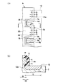
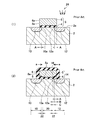
それに対して、図2は、積層構造8の輪郭の一部8bに、凹凸が形成された場合を示している。すなわち、不純物注入領域12の輪郭12aに沿って延びる範囲の輪郭8bに、凹部8dと凸部8eが交互に繰り返し形成されている場合を示す。不純物注入領域12の輪郭12aと無関係に延びる範囲の積層構造8の輪郭8cに関しては、凹凸があってもよいし、なくてもよい。
破線12aは、積層構造8をマスクにして半導体基板2に不純物を注入して形成した不純物注入領域12の輪郭の一部を示している。不純物を斜めに注入することと、注入した不純物が拡散することが影響し、不純物注入領域12の輪郭12aは、積層構造8の輪郭8b、8cから内側に距離Aだけ侵入した位置に形成される。距離Aは図8と図10で説明した距離である。輪郭8bに凹凸が形成されていることに対応して、輪郭12aにも凹凸が形成される。
図2(1)における一点鎖線5aは、図8で説明したバーズビーク5の形成範囲の輪郭を示している。バーズビーク5は酸化することで形成される。したがって、酸素がよく供給される位置ではバーズビーク5がよく発達し、酸素は供給されにくい位置ではバーズビーク5が発達しづらい。凸部8eでは、酸素がよく供給されることから、バーズビーク5が深く侵入する。凸部8eでは、バーズビークの形成範囲の輪郭5aは、積層構造8の輪郭8eから内側に距離Bだけ離れた位置となる。距離Bは図8で説明した距離であり、A<Bである。
それに対して、凹部8dでは、酸素が供給され難い。凹部8dではバーズビーク5がほとんど発達しない。図2では、簡単化のために、凹部8dではバーズビーク5が発達しない場合を図示している。バーズビーク5が形成されなければ、バーズビークの形成範囲の輪郭5aは、積層構造8の輪郭8dに一致する。
凸部8eと凹部8dを接続する範囲の輪郭8gでは、バーズビークの侵入距離が変化する。凸部8eに近い部分では酸素がよく供給され、バーズビークが深くまで侵入する。凹部8dに近い部分では酸素が供給され難く、バーズビークの侵入深さが減少する。
それに対して、凹部8dでは、酸素が供給され難い。凹部8dではバーズビーク5がほとんど発達しない。図2では、簡単化のために、凹部8dではバーズビーク5が発達しない場合を図示している。バーズビーク5が形成されなければ、バーズビークの形成範囲の輪郭5aは、積層構造8の輪郭8dに一致する。
凸部8eと凹部8dを接続する範囲の輪郭8gでは、バーズビークの侵入距離が変化する。凸部8eに近い部分では酸素がよく供給され、バーズビークが深くまで侵入する。凹部8dに近い部分では酸素が供給され難く、バーズビークの侵入深さが減少する。
ハッチで示す範囲18は、不純物注入領域12がバーズビーク5の形成範囲を超えて延びている範囲を示す。すなわち、不純物注入領域12と反転層形成範囲20が重複する範囲を示す。
凹部8dではバーズビーク5が発達しないことから、不純物注入領域12がバーズビーク5の形成範囲を超えて延びている範囲18が得られる。不純物注入領域12と反転層形成範囲20が重複する範囲18が得られると、不純物注入領域12と反転層20が直接的に接触する関係が得られる。図2の(E)は、図2の(1)のE―E断面を示している。凹部8dでは、バーズビークが形成されないことから、薄いゲート酸化膜4が不純物注入領域12内に達している。
凹部8dではバーズビーク5が発達しないことから、不純物注入領域12がバーズビーク5の形成範囲を超えて延びている範囲18が得られる。不純物注入領域12と反転層形成範囲20が重複する範囲18が得られると、不純物注入領域12と反転層20が直接的に接触する関係が得られる。図2の(E)は、図2の(1)のE―E断面を示している。凹部8dでは、バーズビークが形成されないことから、薄いゲート酸化膜4が不純物注入領域12内に達している。
上記のように、不純物注入領域12の輪郭12aに沿って延びる範囲の積層構造の輪郭8bに凹凸が形成されていると、不純物注入領域と反転層が直接的に接触する範囲が得られる。不純物注入領域と反転層がつながらないために抵抗が下がらないという問題が解決される。
なお図2は模式的なものであり、細かく見ると実際の形成範囲と相違していることがある。例えば凹部8dではバーズビークが形成されない場合を図示しているが、凹部8dでもバーズビークが形成されることがある。ただし、凹部8dで形成されるバーズビークはさほど成長せず、A>Bの関係となる。A>Bの関係が得られれば、不純物注入領域と反転層形成範囲がオーバラップする範囲が得られる。不純物注入領域と反転層の間の抵抗が下がらないという問題が解決される。
なお図2は模式的なものであり、細かく見ると実際の形成範囲と相違していることがある。例えば凹部8dではバーズビークが形成されない場合を図示しているが、凹部8dでもバーズビークが形成されることがある。ただし、凹部8dで形成されるバーズビークはさほど成長せず、A>Bの関係となる。A>Bの関係が得られれば、不純物注入領域と反転層形成範囲がオーバラップする範囲が得られる。不純物注入領域と反転層の間の抵抗が下がらないという問題が解決される。
積層構造の輪郭に凹凸を設ける技術は、図10に例示した縦型の半導体装置にも有効であるし、図8と図9に例示した横型の半導体装置にも有効である。
横型の半導体装置に適用する場合は、ゲート絶縁膜とゲート電極の積層構造に隣接する第1範囲に第1不純物注入領域が形成されるとともに、前記積層構造に隣接する第2範囲に第2不純物注入領域が形成される。ここで、第1不純物注入領域の導電型と第2不純物注入領域の導電型は同一であり、ゲート絶縁膜を介してゲート電極に対向する範囲の半導体基板の導電型とは異なる。
第1不純物注入領域と第2不純物注入領域は、図8に例示する場合は高濃度となり、図9に例示する場合は低濃度となる。第1不純物注入領域と第2不純物注入領域の不純物濃度は制約されない。
上記の構造を備えていると、第1不純物注入領域と反転層が直接に接触し、第2不純物注入領域と反転層が直接に接触する。反転層を形成することで第1不純物注入領域と第2不純物注入領域の間の抵抗が顕著に低下する現象が得られる。
横型の半導体装置に適用する場合は、ゲート絶縁膜とゲート電極の積層構造に隣接する第1範囲に第1不純物注入領域が形成されるとともに、前記積層構造に隣接する第2範囲に第2不純物注入領域が形成される。ここで、第1不純物注入領域の導電型と第2不純物注入領域の導電型は同一であり、ゲート絶縁膜を介してゲート電極に対向する範囲の半導体基板の導電型とは異なる。
第1不純物注入領域と第2不純物注入領域は、図8に例示する場合は高濃度となり、図9に例示する場合は低濃度となる。第1不純物注入領域と第2不純物注入領域の不純物濃度は制約されない。
上記の構造を備えていると、第1不純物注入領域と反転層が直接に接触し、第2不純物注入領域と反転層が直接に接触する。反転層を形成することで第1不純物注入領域と第2不純物注入領域の間の抵抗が顕著に低下する現象が得られる。
積層構造と半導体基板が対向する範囲の輪郭に凹凸を設ける技術によると、半導体基板を平面視したときに、積層構造と半導体基板が対向する範囲を定める輪郭の内側に不純物注入領域とバーズビークの形成範囲が形成され、不純物注入領域がバーズビークの形成範囲を超えて延びる範囲が形成される。
本明細書で開示する半導体装置の製造方法は、半導体基板の表面の一部にゲート絶縁膜とゲート電極の積層構造を形成する工程と、その積層構造ごしに半導体基板の表面の一部に不純物を注入する工程と、その積層構造の露出面に熱酸化膜を形成する工程を備えている。本製造方法は、積層構造と半導体基板が対向する範囲を平面視したときに、不純物注入領域の輪郭に沿って延びる積層構造の輪郭に凹凸が形成されていることを特徴とする。
上記製造方法によると、ゲート絶縁膜とゲート電極の積層構造をマスクにして不純物注入領域を規制するとともに、その積層構造を覆う熱酸化膜を形成して半導体装置を製造した場合に、熱酸化膜の形成時に形成されるバーズビークによって不純物注入領域と反転層が分断されるという問題が生じない。
本明細書で開示する技術の詳細、及び、さらなる改良は、発明を実施するための形態、及び実施例にて詳しく説明する。
以下に説明する実施例の主要な特徴を下記に列記する。なお、以下に記載する技術要素は、それぞれが独立した技術要素であって、単独であるいは各種の組合せによって技術的有用性を発揮するものであり、出願時の請求項記載の組合せに限定されるものではない。
(特徴1)ゲート絶縁膜はSiO2であり、ゲート電極はポリシリコンである。
(特徴2)半導体基板は、SiまたはSiCの単結晶である。
(特徴1)ゲート絶縁膜はSiO2であり、ゲート電極はポリシリコンである。
(特徴2)半導体基板は、SiまたはSiCの単結晶である。
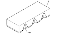
図1は、実施例のゲート絶縁膜4とゲート電極6の積層構造8を示す。積層構造8の輪郭8bは、不純物注入領域に沿って延びる範囲の輪郭であり、輪郭8cは不純物注入領域と無関係に延びる範囲の輪郭である。すなわち、積層構造8をマスクにして半導体基板2に不純物を注入する際に、輪郭8bは不純物注入範囲を律する輪郭となり、輪郭8cは不純物注入範囲を律する輪郭とならない。輪郭8bが延びているY方向をゲートの幅方向といい、輪郭8cが延びているX方向をゲートの長さ方向という。
輪郭8bには、凹部8dと凸部8eが、ゲートの幅方向に交互に繰り返すように形成されている。ゲートの長さ方向に延びる輪郭8cには凹凸を形成する必要はない。
積層構造8をマスクにして半導体基板2に不純物を注入する。その際には、矢印24に示すように、種々の斜め方向から不純物を注入する。
輪郭8bには、凹部8dと凸部8eが、ゲートの幅方向に交互に繰り返すように形成されている。ゲートの長さ方向に延びる輪郭8cには凹凸を形成する必要はない。
積層構造8をマスクにして半導体基板2に不純物を注入する。その際には、矢印24に示すように、種々の斜め方向から不純物を注入する。
図2は、凹部8dのゲートの幅方向の距離を凸部8eのゲートの幅方向の距離よりも狭くした場合を示している。
前記したように、凹部8dではバーズビーク5の発達が抑制されることから、不純物注入領域12がバーズビーク形成範囲をこえて延びる範囲18が得られ、不純物注入領域12と反転層20が直接的に接触する。不純物注入領域12と反転層20が直接的に接触するために、ゲート電極6に電圧を加えて半導体基板2に反転層を形成した場合に、反転層と不純物注入領域12の間の抵抗は顕著に低下する。同様の現象が、不純物注入領域10と反転層20の間でも得られる。図2の構造によると、ゲート電極6に電圧を加えて半導体基板2に反転層を形成した場合に、第1不純物注入領域10と第2不純物注入領域12の間の抵抗は顕著に低下する。
前記したように、凹部8dではバーズビーク5の発達が抑制されることから、不純物注入領域12がバーズビーク形成範囲をこえて延びる範囲18が得られ、不純物注入領域12と反転層20が直接的に接触する。不純物注入領域12と反転層20が直接的に接触するために、ゲート電極6に電圧を加えて半導体基板2に反転層を形成した場合に、反転層と不純物注入領域12の間の抵抗は顕著に低下する。同様の現象が、不純物注入領域10と反転層20の間でも得られる。図2の構造によると、ゲート電極6に電圧を加えて半導体基板2に反転層を形成した場合に、第1不純物注入領域10と第2不純物注入領域12の間の抵抗は顕著に低下する。
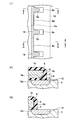
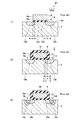
図3は、凸部8eのゲート幅方向の距離を凹部8dのゲート幅方向の距離よりも狭くした場合を示している。特に、凸部8eのゲート幅方向の距離を2×A未満にした場合を示している。Aは、図8を参照して説明した距離である。凸部8eのゲート幅方向の距離を2×A未満にすると、凸部8eの全範囲に不純物注入領域12が形成される。図3の場合、輪郭12aよりも右側の全範囲に不純物注入領域12が形成される。
破線5aはバーズビークの形成範囲を示している。破線5aより右側にはバズビークが形成されるが、破線5aより左側には形成されない。ハッチで示す範囲18は、不純物注入領域がバーズビーク形成範囲を超えて延びる範囲を示している。すなわち、不純物注入領域と反転層が直接に接する範囲を示している。凸部8eのゲート幅方向の距離を短縮化すると、ゲート幅方向の全幅に亘って、不純物注入領域と反転層が直接に接する関係が得られる。図2に比してさらにオン抵抗を下げることができる。
破線5aはバーズビークの形成範囲を示している。破線5aより右側にはバズビークが形成されるが、破線5aより左側には形成されない。ハッチで示す範囲18は、不純物注入領域がバーズビーク形成範囲を超えて延びる範囲を示している。すなわち、不純物注入領域と反転層が直接に接する範囲を示している。凸部8eのゲート幅方向の距離を短縮化すると、ゲート幅方向の全幅に亘って、不純物注入領域と反転層が直接に接する関係が得られる。図2に比してさらにオン抵抗を下げることができる。
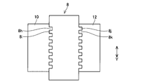
図4は、第3実施例の積層構造8を示している。この場合、ゲート幅方向が同じ位置を観測した場合、凹部8hが形成されている位置では凸部8jが形成されており、凸部8iが形成されている位置では凹部8kが形成されている。この場合、ゲート電極6のゲート長さ方向の距離は、ゲート幅方向のいずれの位置でも等しくなる。第3実施例によると、ゲート電極6に電圧を印加した場合の電流分布が均質化される。
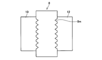
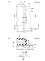
図5は、第4実施例の積層構造8を示している。凹部8mは、三角形の形状であってもよい。あるいは、図6に示すように、半円と直線の組み合わせで凹部を形成してもよい。半円のみからなる凹部であってもよい。
図7は、第6実施例の積層構造を示している。本実施例で重要なのは積層構造が半導体基板に対向する範囲の形状(下面形状)であり、積層構造の上面形状が下面形状に一致する必要はない。凹部8pは、ゲート幅方向に傾斜する壁面を備えていてもよいし、ゲート長さ方向に傾斜する壁面を備えていてもよい。また傾斜壁面が、積層構造の上面に達していてもよいし、達していなくてもよい。本明細書でいう積層構造の輪郭とは、積層構造の下面(半導体基板に対向ないし接する面)の輪郭のことをいう。
以上、本明細書が開示する技術の実施例について詳細に説明したが、これらは例示にすぎず、特許請求の範囲を限定するものではない。特許請求の範囲に記載の技術には、以上に例示した具体例を様々に変形、変更したものが含まれる。
また、本明細書または図面に説明した技術要素は、単独であるいは各種の組合せによって技術的有用性を発揮するものであり、出願時請求項記載の組合せに限定されるものではない。また、本明細書または図面に例示した技術は複数目的を同時に達成するものであり、そのうちの一つの目的を達成すること自体で技術的有用性を持つものである。
また、本明細書または図面に説明した技術要素は、単独であるいは各種の組合せによって技術的有用性を発揮するものであり、出願時請求項記載の組合せに限定されるものではない。また、本明細書または図面に例示した技術は複数目的を同時に達成するものであり、そのうちの一つの目的を達成すること自体で技術的有用性を持つものである。
2:半導体基板
2a:表面
4:ゲート絶縁膜
5:バーズビーク
5a:バーズビークの内側境界
5b:バーズビークの形成範囲
6:ゲート電極
6a:輪郭
8:積層構造
8a:輪郭
8b:不純物注入領域に沿って延びる範囲の輪郭
8c:不純物注入領域と無関係に延びる範囲の輪郭
8d:凹部
8e:凸部
8g:凸部と凹部を結ぶ輪郭
8h、8k、8m、8n、8p:凹部
8i,8j:凸部
10:第1不純物注入領域
10a:内側輪郭
10b:第1不純物低濃度注入領域
10b1:左側第1不純物低濃度注入領域
10b2:右側第1不純物低濃度注入領域
10c:第1不純物高濃度注入領域
10c1:右側第1不純物高濃度注入領域
10c2:右側第1不純物高濃度注入領域
12:第2不純物注入領域
12a:内側輪郭
12b:第2不純物低濃度注入領域
12c:第2不純物高濃度注入領域
13:不純物注入領域がバーズビーク形成範囲を超えて延びている範囲
14:熱酸化後のゲート絶縁膜
16:熱酸化膜
16a:熱酸化膜の輪郭
18:不純物注入領域がバーズビーク形成範囲を超えて延びている範囲
20:反転層形成範囲
22:非連続範囲(高抵抗範囲)
24:注入方向
2a:表面
4:ゲート絶縁膜
5:バーズビーク
5a:バーズビークの内側境界
5b:バーズビークの形成範囲
6:ゲート電極
6a:輪郭
8:積層構造
8a:輪郭
8b:不純物注入領域に沿って延びる範囲の輪郭
8c:不純物注入領域と無関係に延びる範囲の輪郭
8d:凹部
8e:凸部
8g:凸部と凹部を結ぶ輪郭
8h、8k、8m、8n、8p:凹部
8i,8j:凸部
10:第1不純物注入領域
10a:内側輪郭
10b:第1不純物低濃度注入領域
10b1:左側第1不純物低濃度注入領域
10b2:右側第1不純物低濃度注入領域
10c:第1不純物高濃度注入領域
10c1:右側第1不純物高濃度注入領域
10c2:右側第1不純物高濃度注入領域
12:第2不純物注入領域
12a:内側輪郭
12b:第2不純物低濃度注入領域
12c:第2不純物高濃度注入領域
13:不純物注入領域がバーズビーク形成範囲を超えて延びている範囲
14:熱酸化後のゲート絶縁膜
16:熱酸化膜
16a:熱酸化膜の輪郭
18:不純物注入領域がバーズビーク形成範囲を超えて延びている範囲
20:反転層形成範囲
22:非連続範囲(高抵抗範囲)
24:注入方向
Claims (4)
- 半導体基板の表面の一部に形成されているゲート絶縁膜と、
ゲート絶縁膜上に積層されているゲート電極と、
ゲート絶縁膜とゲート電極の積層構造を覆う熱酸化膜と、
前記積層構造に隣接する範囲の半導体基板に形成されている不純物注入領域と、
を備えており、
前記積層構造が半導体基板に対向する範囲を平面視したときに、不純物注入領域の輪郭に沿って延びる範囲の対向範囲の輪郭に、凹凸が形成されていることを特徴とする半導体装置。 - 前記積層構造に隣接する第1範囲に第1不純物注入領域が形成されているとともに前記積層構造に隣接する第2範囲に第2不純物注入領域が形成されており、
第1不純物注入領域の導電型と第2不純物注入領域の導電型が、ゲート絶縁膜を介してゲート電極に対向する範囲の半導体基板の導電型の反対であることを特徴とする請求項1に記載の半導体装置。 - 前記積層構造が半導体基板に対向する範囲を平面視したときに、対向範囲の輪郭から内側に向けて不純物注入領域とバーズビーク形成範囲が延びており、不純物注入領域がバーズビーク形成範囲を超えて延びる部分を備えていることを特徴とする請求項1または2に記載の半導体装置。
- 半導体基板の表面の一部にゲート絶縁膜とゲート電極の積層構造を形成する工程と、
その積層構造ごしに半導体基板の表面の一部に不純物を注入する工程と、
その積層構造の露出面に熱酸化膜を形成する工程を備えており、
前記積層構造が半導体基板に対向する範囲を平面視したときに、不純物注入領域の輪郭に沿って延びる範囲の対向範囲の輪郭に、凹凸が形成されていることを特徴とする半導体装置の製造方法。
Applications Claiming Priority (2)
| Application Number | Priority Date | Filing Date | Title |
|---|---|---|---|
| JP2013184930A JP2015053367A (ja) | 2013-09-06 | 2013-09-06 | 半導体装置とその製造方法 |
| JP2013-184930 | 2013-09-06 |
Publications (1)
| Publication Number | Publication Date |
|---|---|
| WO2015033733A1 true WO2015033733A1 (ja) | 2015-03-12 |
Family
ID=52628216
Family Applications (1)
| Application Number | Title | Priority Date | Filing Date |
|---|---|---|---|
| PCT/JP2014/070845 Ceased WO2015033733A1 (ja) | 2013-09-06 | 2014-08-07 | 半導体装置とその製造方法 |
Country Status (2)
| Country | Link |
|---|---|
| JP (1) | JP2015053367A (ja) |
| WO (1) | WO2015033733A1 (ja) |
Citations (4)
| Publication number | Priority date | Publication date | Assignee | Title |
|---|---|---|---|---|
| JPH02181435A (ja) * | 1989-01-06 | 1990-07-16 | Matsushita Electron Corp | 半導体装置の製造方法 |
| JPH07249767A (ja) * | 1994-03-11 | 1995-09-26 | Fujitsu Ltd | 半導体装置の製造方法 |
| JPH1131819A (ja) * | 1997-07-14 | 1999-02-02 | Matsushita Electron Corp | 静電破壊保護トランジスタ |
| JP2000216373A (ja) * | 1999-01-19 | 2000-08-04 | United Microelectronics Corp | 半導体デバイスの製造方法 |
Family Cites Families (2)
| Publication number | Priority date | Publication date | Assignee | Title |
|---|---|---|---|---|
| JP2850668B2 (ja) * | 1992-10-01 | 1999-01-27 | 日本電気株式会社 | 半導体装置の製造方法 |
| JP5292157B2 (ja) * | 2009-03-31 | 2013-09-18 | 株式会社日立製作所 | 横型絶縁ゲートバイポーラトランジスタおよびその製造方法 |
-
2013
- 2013-09-06 JP JP2013184930A patent/JP2015053367A/ja active Pending
-
2014
- 2014-08-07 WO PCT/JP2014/070845 patent/WO2015033733A1/ja not_active Ceased
Patent Citations (4)
| Publication number | Priority date | Publication date | Assignee | Title |
|---|---|---|---|---|
| JPH02181435A (ja) * | 1989-01-06 | 1990-07-16 | Matsushita Electron Corp | 半導体装置の製造方法 |
| JPH07249767A (ja) * | 1994-03-11 | 1995-09-26 | Fujitsu Ltd | 半導体装置の製造方法 |
| JPH1131819A (ja) * | 1997-07-14 | 1999-02-02 | Matsushita Electron Corp | 静電破壊保護トランジスタ |
| JP2000216373A (ja) * | 1999-01-19 | 2000-08-04 | United Microelectronics Corp | 半導体デバイスの製造方法 |
Also Published As
| Publication number | Publication date |
|---|---|
| JP2015053367A (ja) | 2015-03-19 |
Similar Documents
| Publication | Publication Date | Title |
|---|---|---|
| JP6870546B2 (ja) | 半導体装置およびその製造方法 | |
| CN101981701B (zh) | 半导体装置及其制造方法 | |
| CN105164812B (zh) | 半导体装置以及半导体装置的制造方法 | |
| CN104737296B (zh) | 碳化硅半导体装置及其制造方法 | |
| US8067798B2 (en) | Semiconductor device | |
| US10714611B2 (en) | Silicon carbide semiconductor device | |
| JP5790573B2 (ja) | 炭化珪素半導体装置およびその製造方法 | |
| JP5452876B2 (ja) | 半導体装置およびその製造方法 | |
| US20100155833A1 (en) | Semiconductor device having vertical type MOSFET and manufacturing method thereof | |
| DE112015000140B4 (de) | Halbleitervorrichtung | |
| JP2007515080A (ja) | 超接合デバイスの製造での平坦化方法 | |
| CN106165103A (zh) | 半导体器件及半导体器件的制造方法 | |
| CN101211978A (zh) | 半导体装置 | |
| US20150295024A1 (en) | Semiconductor device having super-junction structures and fabrication thereof | |
| CN108666370A (zh) | 半导体装置 | |
| JP6563689B2 (ja) | 絶縁ゲート型スイッチング素子の製造方法 | |
| WO2015033733A1 (ja) | 半導体装置とその製造方法 | |
| US9570353B1 (en) | Method for manufacturing semiconductor device | |
| JP5502468B2 (ja) | 半導体装置の製造方法および半導体装置 | |
| WO2019093465A1 (ja) | 炭化珪素半導体装置、および、炭化珪素半導体装置の製造方法 | |
| JP7151395B2 (ja) | 半導体装置の製造方法 | |
| JP4381435B2 (ja) | 半導体装置および半導体装置の製造方法 | |
| JP7666114B2 (ja) | 半導体装置 | |
| CN103515382B (zh) | 半导体装置及其制造方法 | |
| JP2012204564A (ja) | 半導体素子及び半導体素子の製造方法 |
Legal Events
| Date | Code | Title | Description |
|---|---|---|---|
| 121 | Ep: the epo has been informed by wipo that ep was designated in this application |
Ref document number: 14841470 Country of ref document: EP Kind code of ref document: A1 |
|
| NENP | Non-entry into the national phase |
Ref country code: DE |
|
| 122 | Ep: pct application non-entry in european phase |
Ref document number: 14841470 Country of ref document: EP Kind code of ref document: A1 |