WO2015033705A1 - 多層基板および多層基板の製造方法 - Google Patents
多層基板および多層基板の製造方法 Download PDFInfo
- Publication number
- WO2015033705A1 WO2015033705A1 PCT/JP2014/070005 JP2014070005W WO2015033705A1 WO 2015033705 A1 WO2015033705 A1 WO 2015033705A1 JP 2014070005 W JP2014070005 W JP 2014070005W WO 2015033705 A1 WO2015033705 A1 WO 2015033705A1
- Authority
- WO
- WIPO (PCT)
- Prior art keywords
- substrate
- resin base
- base material
- resin
- wiring pattern
- Prior art date
- Legal status (The legal status is an assumption and is not a legal conclusion. Google has not performed a legal analysis and makes no representation as to the accuracy of the status listed.)
- Ceased
Links
Images



Classifications
-
- H—ELECTRICITY
- H05—ELECTRIC TECHNIQUES NOT OTHERWISE PROVIDED FOR
- H05K—PRINTED CIRCUITS; CASINGS OR CONSTRUCTIONAL DETAILS OF ELECTRIC APPARATUS; MANUFACTURE OF ASSEMBLAGES OF ELECTRICAL COMPONENTS
- H05K1/00—Printed circuits
- H05K1/02—Details
- H05K1/11—Printed elements for providing electric connections to or between printed circuits
- H05K1/115—Via connections; Lands around holes or via connections
-
- B—PERFORMING OPERATIONS; TRANSPORTING
- B32—LAYERED PRODUCTS
- B32B—LAYERED PRODUCTS, i.e. PRODUCTS BUILT-UP OF STRATA OF FLAT OR NON-FLAT, e.g. CELLULAR OR HONEYCOMB, FORM
- B32B7/00—Layered products characterised by the relation between layers; Layered products characterised by the relative orientation of features between layers, or by the relative values of a measurable parameter between layers, i.e. products comprising layers having different physical, chemical or physicochemical properties; Layered products characterised by the interconnection of layers
- B32B7/03—Layered products characterised by the relation between layers; Layered products characterised by the relative orientation of features between layers, or by the relative values of a measurable parameter between layers, i.e. products comprising layers having different physical, chemical or physicochemical properties; Layered products characterised by the interconnection of layers with respect to the orientation of features
-
- B—PERFORMING OPERATIONS; TRANSPORTING
- B32—LAYERED PRODUCTS
- B32B—LAYERED PRODUCTS, i.e. PRODUCTS BUILT-UP OF STRATA OF FLAT OR NON-FLAT, e.g. CELLULAR OR HONEYCOMB, FORM
- B32B27/00—Layered products comprising a layer of synthetic resin
- B32B27/06—Layered products comprising a layer of synthetic resin as the main or only constituent of a layer, which is next to another layer of the same or of a different material
- B32B27/08—Layered products comprising a layer of synthetic resin as the main or only constituent of a layer, which is next to another layer of the same or of a different material of synthetic resin
-
- B—PERFORMING OPERATIONS; TRANSPORTING
- B32—LAYERED PRODUCTS
- B32B—LAYERED PRODUCTS, i.e. PRODUCTS BUILT-UP OF STRATA OF FLAT OR NON-FLAT, e.g. CELLULAR OR HONEYCOMB, FORM
- B32B27/00—Layered products comprising a layer of synthetic resin
- B32B27/28—Layered products comprising a layer of synthetic resin comprising synthetic resins not wholly covered by any one of the sub-groups B32B27/30 - B32B27/42
- B32B27/281—Layered products comprising a layer of synthetic resin comprising synthetic resins not wholly covered by any one of the sub-groups B32B27/30 - B32B27/42 comprising polyimides
-
- B—PERFORMING OPERATIONS; TRANSPORTING
- B32—LAYERED PRODUCTS
- B32B—LAYERED PRODUCTS, i.e. PRODUCTS BUILT-UP OF STRATA OF FLAT OR NON-FLAT, e.g. CELLULAR OR HONEYCOMB, FORM
- B32B27/00—Layered products comprising a layer of synthetic resin
- B32B27/28—Layered products comprising a layer of synthetic resin comprising synthetic resins not wholly covered by any one of the sub-groups B32B27/30 - B32B27/42
- B32B27/285—Layered products comprising a layer of synthetic resin comprising synthetic resins not wholly covered by any one of the sub-groups B32B27/30 - B32B27/42 comprising polyethers
-
- B—PERFORMING OPERATIONS; TRANSPORTING
- B32—LAYERED PRODUCTS
- B32B—LAYERED PRODUCTS, i.e. PRODUCTS BUILT-UP OF STRATA OF FLAT OR NON-FLAT, e.g. CELLULAR OR HONEYCOMB, FORM
- B32B27/00—Layered products comprising a layer of synthetic resin
- B32B27/28—Layered products comprising a layer of synthetic resin comprising synthetic resins not wholly covered by any one of the sub-groups B32B27/30 - B32B27/42
- B32B27/286—Layered products comprising a layer of synthetic resin comprising synthetic resins not wholly covered by any one of the sub-groups B32B27/30 - B32B27/42 comprising polysulphones; polysulfides
-
- B—PERFORMING OPERATIONS; TRANSPORTING
- B32—LAYERED PRODUCTS
- B32B—LAYERED PRODUCTS, i.e. PRODUCTS BUILT-UP OF STRATA OF FLAT OR NON-FLAT, e.g. CELLULAR OR HONEYCOMB, FORM
- B32B37/00—Methods or apparatus for laminating, e.g. by curing or by ultrasonic bonding
- B32B37/02—Methods or apparatus for laminating, e.g. by curing or by ultrasonic bonding characterised by a sequence of laminating steps, e.g. by adding new layers at consecutive laminating stations
-
- B—PERFORMING OPERATIONS; TRANSPORTING
- B32—LAYERED PRODUCTS
- B32B—LAYERED PRODUCTS, i.e. PRODUCTS BUILT-UP OF STRATA OF FLAT OR NON-FLAT, e.g. CELLULAR OR HONEYCOMB, FORM
- B32B37/00—Methods or apparatus for laminating, e.g. by curing or by ultrasonic bonding
- B32B37/06—Methods or apparatus for laminating, e.g. by curing or by ultrasonic bonding characterised by the heating method
-
- B—PERFORMING OPERATIONS; TRANSPORTING
- B32—LAYERED PRODUCTS
- B32B—LAYERED PRODUCTS, i.e. PRODUCTS BUILT-UP OF STRATA OF FLAT OR NON-FLAT, e.g. CELLULAR OR HONEYCOMB, FORM
- B32B37/00—Methods or apparatus for laminating, e.g. by curing or by ultrasonic bonding
- B32B37/10—Methods or apparatus for laminating, e.g. by curing or by ultrasonic bonding characterised by the pressing technique, e.g. using action of vacuum or fluid pressure
-
- B—PERFORMING OPERATIONS; TRANSPORTING
- B32—LAYERED PRODUCTS
- B32B—LAYERED PRODUCTS, i.e. PRODUCTS BUILT-UP OF STRATA OF FLAT OR NON-FLAT, e.g. CELLULAR OR HONEYCOMB, FORM
- B32B37/00—Methods or apparatus for laminating, e.g. by curing or by ultrasonic bonding
- B32B37/14—Methods or apparatus for laminating, e.g. by curing or by ultrasonic bonding characterised by the properties of the layers
- B32B37/16—Methods or apparatus for laminating, e.g. by curing or by ultrasonic bonding characterised by the properties of the layers with all layers existing as coherent layers before laminating
- B32B37/18—Methods or apparatus for laminating, e.g. by curing or by ultrasonic bonding characterised by the properties of the layers with all layers existing as coherent layers before laminating involving the assembly of discrete sheets or panels only
- B32B37/182—Methods or apparatus for laminating, e.g. by curing or by ultrasonic bonding characterised by the properties of the layers with all layers existing as coherent layers before laminating involving the assembly of discrete sheets or panels only one or more of the layers being plastic
-
- B—PERFORMING OPERATIONS; TRANSPORTING
- B32—LAYERED PRODUCTS
- B32B—LAYERED PRODUCTS, i.e. PRODUCTS BUILT-UP OF STRATA OF FLAT OR NON-FLAT, e.g. CELLULAR OR HONEYCOMB, FORM
- B32B7/00—Layered products characterised by the relation between layers; Layered products characterised by the relative orientation of features between layers, or by the relative values of a measurable parameter between layers, i.e. products comprising layers having different physical, chemical or physicochemical properties; Layered products characterised by the interconnection of layers
- B32B7/04—Interconnection of layers
-
- H—ELECTRICITY
- H05—ELECTRIC TECHNIQUES NOT OTHERWISE PROVIDED FOR
- H05K—PRINTED CIRCUITS; CASINGS OR CONSTRUCTIONAL DETAILS OF ELECTRIC APPARATUS; MANUFACTURE OF ASSEMBLAGES OF ELECTRICAL COMPONENTS
- H05K1/00—Printed circuits
- H05K1/02—Details
- H05K1/0213—Electrical arrangements not otherwise provided for
- H05K1/0237—High frequency adaptations
-
- H—ELECTRICITY
- H05—ELECTRIC TECHNIQUES NOT OTHERWISE PROVIDED FOR
- H05K—PRINTED CIRCUITS; CASINGS OR CONSTRUCTIONAL DETAILS OF ELECTRIC APPARATUS; MANUFACTURE OF ASSEMBLAGES OF ELECTRICAL COMPONENTS
- H05K1/00—Printed circuits
- H05K1/02—Details
- H05K1/03—Use of materials for the substrate
- H05K1/0313—Organic insulating material
- H05K1/0353—Organic insulating material consisting of two or more materials, e.g. two or more polymers, polymer + filler, + reinforcement
-
- H—ELECTRICITY
- H05—ELECTRIC TECHNIQUES NOT OTHERWISE PROVIDED FOR
- H05K—PRINTED CIRCUITS; CASINGS OR CONSTRUCTIONAL DETAILS OF ELECTRIC APPARATUS; MANUFACTURE OF ASSEMBLAGES OF ELECTRICAL COMPONENTS
- H05K3/00—Apparatus or processes for manufacturing printed circuits
- H05K3/02—Apparatus or processes for manufacturing printed circuits in which the conductive material is applied to the surface of the insulating support and is thereafter removed from such areas of the surface which are not intended for current conducting or shielding
- H05K3/06—Apparatus or processes for manufacturing printed circuits in which the conductive material is applied to the surface of the insulating support and is thereafter removed from such areas of the surface which are not intended for current conducting or shielding the conductive material being removed chemically or electrolytically, e.g. by photo-etch process
-
- H—ELECTRICITY
- H05—ELECTRIC TECHNIQUES NOT OTHERWISE PROVIDED FOR
- H05K—PRINTED CIRCUITS; CASINGS OR CONSTRUCTIONAL DETAILS OF ELECTRIC APPARATUS; MANUFACTURE OF ASSEMBLAGES OF ELECTRICAL COMPONENTS
- H05K3/00—Apparatus or processes for manufacturing printed circuits
- H05K3/10—Apparatus or processes for manufacturing printed circuits in which conductive material is applied to the insulating support in such a manner as to form the desired conductive pattern
- H05K3/12—Apparatus or processes for manufacturing printed circuits in which conductive material is applied to the insulating support in such a manner as to form the desired conductive pattern using thick film techniques, e.g. printing techniques to apply the conductive material or similar techniques for applying conductive paste or ink patterns
- H05K3/1216—Apparatus or processes for manufacturing printed circuits in which conductive material is applied to the insulating support in such a manner as to form the desired conductive pattern using thick film techniques, e.g. printing techniques to apply the conductive material or similar techniques for applying conductive paste or ink patterns by screen printing or stencil printing
-
- H—ELECTRICITY
- H05—ELECTRIC TECHNIQUES NOT OTHERWISE PROVIDED FOR
- H05K—PRINTED CIRCUITS; CASINGS OR CONSTRUCTIONAL DETAILS OF ELECTRIC APPARATUS; MANUFACTURE OF ASSEMBLAGES OF ELECTRICAL COMPONENTS
- H05K3/00—Apparatus or processes for manufacturing printed circuits
- H05K3/46—Manufacturing multilayer circuits
- H05K3/4611—Manufacturing multilayer circuits by laminating two or more circuit boards
- H05K3/4626—Manufacturing multilayer circuits by laminating two or more circuit boards characterised by the insulating layers or materials
- H05K3/4632—Manufacturing multilayer circuits by laminating two or more circuit boards characterised by the insulating layers or materials laminating thermoplastic or uncured resin sheets comprising printed circuits without added adhesive materials between the sheets
-
- H—ELECTRICITY
- H05—ELECTRIC TECHNIQUES NOT OTHERWISE PROVIDED FOR
- H05K—PRINTED CIRCUITS; CASINGS OR CONSTRUCTIONAL DETAILS OF ELECTRIC APPARATUS; MANUFACTURE OF ASSEMBLAGES OF ELECTRICAL COMPONENTS
- H05K3/00—Apparatus or processes for manufacturing printed circuits
- H05K3/46—Manufacturing multilayer circuits
- H05K3/4644—Manufacturing multilayer circuits by building the multilayer layer by layer, i.e. build-up multilayer circuits
-
- H—ELECTRICITY
- H05—ELECTRIC TECHNIQUES NOT OTHERWISE PROVIDED FOR
- H05K—PRINTED CIRCUITS; CASINGS OR CONSTRUCTIONAL DETAILS OF ELECTRIC APPARATUS; MANUFACTURE OF ASSEMBLAGES OF ELECTRICAL COMPONENTS
- H05K3/00—Apparatus or processes for manufacturing printed circuits
- H05K3/46—Manufacturing multilayer circuits
- H05K3/4688—Composite multilayer circuits, i.e. comprising insulating layers having different properties
- H05K3/4694—Partitioned multilayer circuits having adjacent regions with different properties, e.g. by adding or inserting locally circuit layers having a higher circuit density
-
- B—PERFORMING OPERATIONS; TRANSPORTING
- B32—LAYERED PRODUCTS
- B32B—LAYERED PRODUCTS, i.e. PRODUCTS BUILT-UP OF STRATA OF FLAT OR NON-FLAT, e.g. CELLULAR OR HONEYCOMB, FORM
- B32B2250/00—Layers arrangement
- B32B2250/24—All layers being polymeric
-
- B—PERFORMING OPERATIONS; TRANSPORTING
- B32—LAYERED PRODUCTS
- B32B—LAYERED PRODUCTS, i.e. PRODUCTS BUILT-UP OF STRATA OF FLAT OR NON-FLAT, e.g. CELLULAR OR HONEYCOMB, FORM
- B32B2255/00—Coating on the layer surface
- B32B2255/10—Coating on the layer surface on synthetic resin layer or on natural or synthetic rubber layer
-
- B—PERFORMING OPERATIONS; TRANSPORTING
- B32—LAYERED PRODUCTS
- B32B—LAYERED PRODUCTS, i.e. PRODUCTS BUILT-UP OF STRATA OF FLAT OR NON-FLAT, e.g. CELLULAR OR HONEYCOMB, FORM
- B32B2255/00—Coating on the layer surface
- B32B2255/20—Inorganic coating
- B32B2255/205—Metallic coating
-
- B—PERFORMING OPERATIONS; TRANSPORTING
- B32—LAYERED PRODUCTS
- B32B—LAYERED PRODUCTS, i.e. PRODUCTS BUILT-UP OF STRATA OF FLAT OR NON-FLAT, e.g. CELLULAR OR HONEYCOMB, FORM
- B32B2457/00—Electrical equipment
- B32B2457/08—PCBs, i.e. printed circuit boards
-
- H—ELECTRICITY
- H05—ELECTRIC TECHNIQUES NOT OTHERWISE PROVIDED FOR
- H05K—PRINTED CIRCUITS; CASINGS OR CONSTRUCTIONAL DETAILS OF ELECTRIC APPARATUS; MANUFACTURE OF ASSEMBLAGES OF ELECTRICAL COMPONENTS
- H05K2201/00—Indexing scheme relating to printed circuits covered by H05K1/00
- H05K2201/01—Dielectrics
- H05K2201/0137—Materials
- H05K2201/0141—Liquid crystal polymer [LCP]
-
- H—ELECTRICITY
- H05—ELECTRIC TECHNIQUES NOT OTHERWISE PROVIDED FOR
- H05K—PRINTED CIRCUITS; CASINGS OR CONSTRUCTIONAL DETAILS OF ELECTRIC APPARATUS; MANUFACTURE OF ASSEMBLAGES OF ELECTRICAL COMPONENTS
- H05K2201/00—Indexing scheme relating to printed circuits covered by H05K1/00
- H05K2201/01—Dielectrics
- H05K2201/0137—Materials
- H05K2201/0154—Polyimide
-
- H—ELECTRICITY
- H05—ELECTRIC TECHNIQUES NOT OTHERWISE PROVIDED FOR
- H05K—PRINTED CIRCUITS; CASINGS OR CONSTRUCTIONAL DETAILS OF ELECTRIC APPARATUS; MANUFACTURE OF ASSEMBLAGES OF ELECTRICAL COMPONENTS
- H05K3/00—Apparatus or processes for manufacturing printed circuits
- H05K3/46—Manufacturing multilayer circuits
- H05K3/4611—Manufacturing multilayer circuits by laminating two or more circuit boards
- H05K3/4614—Manufacturing multilayer circuits by laminating two or more circuit boards the electrical connections between the circuit boards being made during lamination
- H05K3/4617—Manufacturing multilayer circuits by laminating two or more circuit boards the electrical connections between the circuit boards being made during lamination characterized by laminating only or mainly similar single-sided circuit boards
-
- H—ELECTRICITY
- H05—ELECTRIC TECHNIQUES NOT OTHERWISE PROVIDED FOR
- H05K—PRINTED CIRCUITS; CASINGS OR CONSTRUCTIONAL DETAILS OF ELECTRIC APPARATUS; MANUFACTURE OF ASSEMBLAGES OF ELECTRICAL COMPONENTS
- H05K3/00—Apparatus or processes for manufacturing printed circuits
- H05K3/46—Manufacturing multilayer circuits
- H05K3/4697—Manufacturing multilayer circuits having cavities, e.g. for mounting components
Definitions
- the present invention relates to a multilayer substrate having a structure in which a plurality of resin base materials made of a thermoplastic resin are laminated and a method for manufacturing the same.
- the multi-layer substrate of Patent Document 1 constitutes a high frequency circuit by forming a wiring pattern on each resin base material and then laminating and bonding them.
- a resin base material is arranged over the entire surface in a plan view. That is, the resin base material of each layer is provided over the entire area of the multilayer substrate in plan view, and the number of layers and the position of the layers are aligned throughout the entire area of the multilayer substrate.
- the number of layers of the resin base material in other parts is determined according to the part that requires the most number of layers, the number of layers in other parts is more than necessary with respect to the position of the wiring pattern. May end up. At this time, when it is necessary to connect wiring patterns provided in different layers (interlayer connection), the number of connection portions by via conductors increases more than necessary, and the continuity of the interlayer connection is likely to decrease.
- an object of the present invention is to provide a multilayer substrate having a high degree of design freedom and a method for manufacturing the same.
- the multilayer substrate of the present invention is a multilayer substrate in which a plurality of resin base materials made of the same kind of thermoplastic resin are laminated, and is constituted by a plurality of first resin base materials among the plurality of resin base materials. 1 substrate and a second substrate constituted by a plurality of second resin base materials among the plurality of resin base materials, wherein the first substrate and the second substrate are made of the plurality of resin base materials.
- the adjacent positions of the plurality of first resin bases that are arranged adjacent to each other in the stacking direction and that constitute the first substrate, and the interlayers of the plurality of second resin bases that constitute the second substrate The position is different from the position in the stacking direction.
- the multilayer substrate of the present invention can partially vary the number of layers and the interlayer position by disposing the interlayer position of the first substrate and the interlayer position of the second substrate at different positions in the stacking direction. Since it is possible, the degree of freedom of design increases. Thereby, for example, even in a case where it is desired to reduce the facing distance of the wiring pattern in some parts and increase the capacitance value of the capacitor, and in other parts to increase the facing distance of the wiring pattern to suppress the generation of stray capacitance, Each part can be set to an optimum number of layers and interlayer positions.
- first substrate a part of the multilayer substrate (first substrate) is separated from the other part (second substrate).
- second substrate Prepared (for example, purchased or manufactured) and can be easily integrated with the other parts.
- a high-precision base material a high-quality base material with small variations in thickness and dielectric constant
- a process for example, photolithography
- the multilayer substrate of the present invention includes the number of stacked first resin bases constituting the first substrate and the second adjacent to the first substrate among the plurality of second resin bases constituting the second substrate. It is also possible to adopt a mode in which the number of laminated resin base materials is different.
- the minimum number of stacked layers for the wiring pattern can be set for each of the first substrate and the second substrate, so that the number of locations for interlayer connection can be reduced. Further, for example, if the inductor is formed in a portion having a large number of layers, the number of turns of the inductor can be easily increased.
- the first substrate can be more firmly fixed by enclosing the first substrate in the second substrate. Further, the main surface of the multilayer substrate can be formed into a flat plate shape without unevenness, and surface mounting can be easily performed.
- the multilayer substrate of the present invention may have a mode in which the first substrate and the second substrate are conductively joined via via conductors.
- the via conductor (conductive paste) in the second resin base material is metallized.
- the interface between the wiring pattern on the first substrate side and the via conductor of the second substrate is firmly bonded, so that it is possible to suppress peeling.
- the first substrate of the multilayer substrate of the present invention may constitute at least a part of the high frequency filter circuit.
- high frequency circuits are often required to have high accuracy, only the first substrate constituting at least a part of the high frequency filter circuit can be manufactured so as to satisfy high required accuracy.
- a high-accuracy high-frequency filter circuit can be obtained while preventing an increase in manufacturing cost for the entire substrate.
- the multilayer substrate of the present invention is manufactured by first laminating a first resin base material and manufacturing the first substrate by hot pressing, as shown in the following steps (1) to (4).
- the second resin base material is laminated adjacently and manufactured by hot pressing.
- First laminating step of laminating a plurality of first resin base materials among a plurality of resin base materials (2) Heating and pressurizing in a state of laminating a plurality of first resin base materials 1st thermocompression-bonding process which manufactures a 1st board
- Second Laminating Step of Laminating Adjacent to the Substrate (4) The second substrate is manufactured by heating and pressurizing and bonding the first substrate and the plurality of second resin base materials adjacent to each other.
- Second thermocompression bonding step for joining one substrate and a second substrate when the first substrate constitutes at least a part of the high-frequency filter circuit as described above, the first wiring for forming the wiring pattern of the first substrate Highly accurate in pattern formation process It is preferable to use a relatively low accuracy process (for example, screen printing) in the second wiring pattern forming step for forming the wiring pattern of the second substrate by using a different process (for example, photolithography).
- a relatively low accuracy process for example, screen printing
- a different process for example, photolithography
- the degree of freedom in designing the multilayer substrate can be increased.
- FIG. 10 is a side cross-sectional view of a multilayer substrate according to Modification 2.
- FIG. 10 is a side cross-sectional view of a multilayer substrate according to Modification 3.
- FIG. 3 is an exploded perspective view, a side sectional view, and an equivalent circuit diagram of a multilayer substrate when the first substrate constitutes a high-frequency circuit.
- 10 is a side cross-sectional view of a multilayer substrate according to Modification 4.
- FIG. 1A is a perspective view of the multilayer substrate 10.
- FIG. 1B is a side cross-sectional view of the multilayer substrate 10 at a position indicated by A-A ′ in FIG.
- the multilayer substrate 10 includes a first substrate 11, a second substrate 12, and a terminal portion 15.
- the mounting terminal portion 15 is disposed on the lower surface (lower main surface) of the second substrate 12.
- the main surface of the second substrate has a larger area than the main surface of the first substrate, and has a rectangular parallelepiped shape that is long in one direction in plan view.
- the first substrate 11 is formed by laminating a resin base material 111, a resin base material 112, and a resin base material 113. These resin base material 111, resin base material 112, and resin base material 113 are examples of the first resin base material of the present invention.
- the second substrate 12 is formed by laminating a resin base material 121, a resin base material 122, and a resin base material 123. These resin base material 121, resin base material 122, and resin base material 123 are examples of the second resin base material of the present invention.
- Resin base material 111, resin base material 112, and resin base material 113 are made of the same kind of thermoplastic resin.
- the thermoplastic resin is, for example, a liquid crystal polymer resin.
- the thermoplastic resin other than the liquid crystal polymer resin include PEEK (polyether ether ketone), PEI (polyether imide), PPS (poniphenylene sulfide), PI (polyimide), etc., and the liquid crystal polymer resin. These may be used instead of.
- Resin base 121, resin base 122 and resin base 123 are also made of the same kind of thermoplastic resin.
- the thermoplastic resin is, for example, a liquid crystal polymer resin. Therefore, the first substrate 11 and the second substrate 12 are made of the same kind of thermoplastic resin, and the multilayer substrate 10 is made by laminating a plurality of resin base materials made of the same kind of thermoplastic resin.
- the first substrate 11 and the second substrate 12 are arranged adjacent to each other at positions overlapping each other in the resin base material stacking direction.
- the resin base material 112 and the resin base material 113 of the first substrate 11 and the resin base material 121 of the second substrate 12 are arranged adjacent to each other. That is, the first substrate 11 is fitted into a notch portion (cavity portion) formed in the resin base material 121 constituting the upper surface (upper main surface) of the second substrate 12 and stacked on the upper surface of the resin base material 122. Rarely, it is fixed to the second substrate 12.
- the wiring pattern 115 is formed on the upper surface of the resin base material 111 of the first substrate 11.
- the resin substrate 112 has a wiring pattern 116 formed on the upper surface.
- the resin base material 113 has a wiring pattern 117 formed on the lower surface.
- the wiring pattern 125 is formed on the lower surface of the resin substrate 121 of the second substrate.
- the resin substrate 122 has a wiring pattern 126 formed on the lower surface.
- the resin substrate 123 has a wiring pattern 127 formed on the lower surface.
- the wiring pattern 127 is an electrode for connecting the terminal portion 15.
- the wiring pattern 117 is connected to the wiring pattern 126 through the via conductor 131 formed in the resin base material 122.
- the first substrate 11 and the second substrate 12 are conductively joined via the via conductor 131.
- Such a multilayer substrate 10 is manufactured by first laminating each resin substrate of the first substrate 11 and hot pressing, and then laminating the resin substrates of the first substrate 11 and the second substrate 12 adjacent to each other, Manufactured by hot pressing again.
- FIG. 2 is a diagram showing a method for manufacturing the first substrate 11.
- substrate 11 consists of the process of preparing a resin base material first, as shown to FIG. 2 (A).
- the resin base material is prepared by cutting out a required area from a resin sheet in a state in which a conductor foil (for example, copper) is pasted on the entire surface of one side.
- a conductor foil for example, copper
- the wiring pattern 117 is formed by patterning the copper foil 117A.
- photolithography is used as a process for forming a wiring pattern. That is, as shown in FIG. 2B, a resist 51 is applied to the entire surface of the resin base material 113 on which the copper foil 117A is attached, and then exposed using a mask corresponding to the wiring pattern. As shown in FIG. 2C, the resist 51 other than the portion corresponding to the wiring pattern is removed by development. Then, as shown in FIG. 2D, etching is performed to remove the copper foil 117A other than the portion corresponding to the wiring pattern. Finally, the resist 51 is removed and a wiring pattern 117 is formed.
- the same process is also performed on the resin base material 111 and the resin base material 112, and the wiring pattern 115 and the wiring pattern 116 are formed, respectively.
- the resin base material 111, the resin base material 112, and the resin base material 113 are stacked (an example of the first stacking step of the present invention).
- 2A to 2E show a diagram in which the wiring pattern 117 is arranged on the upper surface side for the sake of explanation. However, at the time of stacking, as shown in FIG. 2F, the wiring pattern 117 is shown. Is disposed on the lower surface side.
- heating and pressurizing are performed by a heating press (an example of the first thermocompression bonding step of the present invention).
- each resin base material is temporarily press-bonded (temporary bonding), and the first substrate 11 is manufactured.
- the wiring pattern of each resin substrate is electrically connected by a via conductor.
- the via conductor is temporarily joined with a conductive paste buried in a through-hole of each resin base material (through only the resin base material with a carbon dioxide laser or the like) at the time of heating press in FIG.
- the multilayer substrate 10 is manufactured by laminating the resin substrates of the first substrate 11 and the second substrate 12 so as to be adjacent to each other at positions where they overlap each other in the lamination direction of the resin substrates, and performing hot pressing.
- a resin base material 122 is prepared by cutting out a required area from a resin sheet in which a conductive foil (for example, copper) 126A is previously attached to the entire surface of one side.
- a conductive foil for example, copper
- a predetermined wiring pattern is formed on the copper foil 126A.
- screen printing is used as a process for forming a wiring pattern. That is, as shown in FIG. 3B, a resist 51 is printed on a portion corresponding to the wiring pattern on the surface of the resin base material 122 on which the copper foil 126A is attached.
- the copper foil 126A other than the portion corresponding to the wiring pattern is removed by etching or the like.
- the resist 51 is removed and a wiring pattern 126 is formed.
- the same process is also performed on the resin base material 121 and the resin base material 123, and the wiring pattern 125 and the wiring pattern 127 are formed, respectively.
- the resin base material 122 is formed with a through-hole 53 in a part of the resin base material 122 by a carbon dioxide laser or the like, and then, as shown in FIG.
- the through-hole 53 is filled with the conductive paste 131A.
- the resin base material 121, the resin base material 122, and the resin base material 123 are laminated
- the first substrate 11 is fitted into a notch portion (cavity portion) formed in the resin base material 121 and stacked on the upper surface of the resin base material 122. That is, the first substrate 11 is disposed adjacent to the resin base 121 and laminated.
- the first substrate 11 is bonded to the second substrate 12 at the side surface and the bottom surface, so that the bonding strength is increased.
- the side surface of the cavity portion serves as a guide, the accuracy of the position where the first substrate 11 is disposed is increased.
- 3A to 3F show the wiring pattern 126 disposed on the upper surface side for the sake of explanation, the wiring pattern 126 is shown in FIG. 4A when stacked. Is disposed on the lower surface side.
- thermocompression bonding step of the present invention After laminating each resin base material for constituting the second substrate 12 and the first substrate 11, as shown in FIG. 4B, heating and pressurizing with a hot press machine (second thermocompression bonding step of the present invention) Is an example). In this way, the second substrate 12 is manufactured, and the first substrate 11 and the second substrate 12 are firmly bonded. Note that the terminal portion 15 is mounted on the wiring pattern 127 exposed on the lower surface of the resin base material 123 by solder or the like.
- first substrate 11 and the second substrate 12 are formed by welding resin base materials made of the same kind of thermoplastic resin, each resin base material is heated and pressed between the first substrate 11 and the second substrate 12. Sometimes it is filled by flowing in, and the boundary surface is firmly joined and integrated. Therefore, it is possible to prevent the occurrence of stress and deformation due to the difference in the linear expansion coefficient between the laminates, so that peeling occurs between the layers of each resin base material and at the interface between the first substrate 11 and the second substrate 12. Can be suppressed.
- the conductive paste 131A in the resin base material 122 is metalized, whereby the wiring of the first substrate 11 is performed.
- the interface between the pattern 117 and the via conductor 131 is firmly bonded, and it is also possible to suppress peeling.
- the interlayer positions of the plurality of first resin bases constituting the first substrate 11 and the interlayer positions of the plurality of second resin bases constituting the second substrate 12 are The plurality of resin base materials are arranged so as to be different in the stacking direction.
- the position of the interlayer 80 between the resin base material 112 of the first substrate 11 and the resin base material 113 is substantially in the middle of the stacking direction of the resin base material 121 of the second substrate 12. It exists and is different from the position between the layers of each resin base material on the second substrate 12.
- the multilayer substrate 10 has portions where the positions between the layers are partially different, the degree of freedom in design is increased. For example, even if there are some places where wiring is required at different positions in the stacking direction, it is necessary to place the same resin base material over the entire surface (all areas of the multilayer board in plan view) up to places where wiring is not required Disappears.
- first substrate 11 and the second substrate 12 made of the same kind of thermoplastic resin adjacent to each other, a part of the multilayer substrate 10 (the first substrate 11) is replaced with another portion (the second substrate). 12) can be prepared separately (for example, purchased or manufactured) and easily integrated with the other parts.
- a high-precision base material for example, a high-quality resin base material with little variation in thickness and dielectric constant
- a high-precision base material is used for the entire multilayer substrate. There is no need.
- the thicknesses of the wiring pattern 117 and the wiring pattern 125 can be changed. Even if the positions between the layers are the same, the thickness of some wirings can be changed. In addition, it becomes easy to manufacture a multilayer substrate having various wiring structures.
- FIG. 5A is a diagram (an exploded cross-sectional view) illustrating a second stacking process when manufacturing the multilayer substrate 10B according to the first modification
- FIG. 5B is a side view illustrating the structure of the multilayer substrate 10B. It is sectional drawing. 5A and 5B, the same components as those in the multilayer substrate 10 shown in FIGS. 4A and 4B are denoted by the same reference numerals, and description thereof is omitted.
- the multilayer substrate 10B is formed by laminating the resin substrate 152 disposed on the upper surface of the resin substrate 122 and the first substrate 11 among the resin substrates for configuring the second substrate 12B, Further, a resin base material 151 is laminated on the entire upper surface. Thereby, the first substrate 11 is included in the second substrate 12B. In this case, at the time of hot pressing, a part of the resin base material 151 flows into the gap between the first substrate 11 and the second substrate 12B, so that the boundary surface is more firmly bonded. Further, the upper surface of the multilayer substrate 10B can be formed into a flat plate shape without unevenness, and surface mounting can be easily performed.
- FIG. 6 is a side sectional view showing the structure of the multilayer substrate 10C according to the second modification. Also in FIG. 6, the same components as those of the multilayer substrate 10 shown in FIG.
- the multilayer substrate 10C according to Modification 2 includes the number of resin base materials constituting the first substrate 11 and the resin base materials adjacent to the first substrate 11 among the second substrates 12C (resin base materials 153 in order from the lower surface side).
- the number of layers of the resin base material 154 and the resin base material 155) is the same.
- the first substrate 11 is also included in the multilayer substrate 10C. It arrange
- the number of adjacent resin base materials may be the same or different.
- the required minimum number of stacked layers for the wiring pattern can be set for each of the first substrate and the second substrate, so that the number of locations for interlayer connection can be reduced.
- the inductor is formed in a portion having a large number of layers, the number of windings of the inductor can be easily increased. Even if the number of stacked layers is the same, the opposing spacing of the wiring pattern can be changed between the first substrate and the second substrate by making the thickness of the resin base material different between the first substrate and the second substrate.
- the capacitor is formed in a portion where the facing distance of the wiring pattern is small, the facing area can be reduced by the small facing distance of the wiring pattern, so the capacitor is formed in a smaller space in plan view. be able to.
- the facing distance between the wiring patterns can be increased, and the generation of stray capacitance can be easily suppressed.
- FIG. 7 is a side sectional view showing the structure of the multilayer substrate 10D according to Modification 3.
- the same components as those of the multilayer substrate 10 shown in FIG. 7 are identical to those of the multilayer substrate 10 shown in FIG.
- the number of resin base materials constituting the first substrate 11B is the number of resin base materials adjacent to the first substrate 11B in the second substrate 12C (resin base materials 153 in order from the lower surface side).
- the number of layers of the resin base material 154 and the resin base material 155) is smaller.
- the first resin base material constituting the first substrate 11B and the second resin base material constituting the second substrate 12C are arranged so that the positions between the layers are different.
- the multilayer substrate of the present invention may be configured such that the number of laminated resin bases on the first substrate side is small.
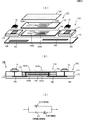
- FIG. 8 (A) is an exploded perspective view of the multilayer substrate when the first substrate constitutes a high-frequency circuit.
- FIG. 8B is a side sectional view
- FIG. 8C is an equivalent circuit diagram.
- the multilayer substrate 10E in this example includes a first substrate 11C, a second substrate 12D, and a terminal portion 15.
- the first substrate 11C constitutes a part of the high frequency filter circuit.
- the first substrate 11C is formed by laminating a resin base material 181, a resin base material 182 and a resist layer 191 in order from the lower surface side.
- the uppermost surface may be a resin base material instead of the resist layer 191.
- the second substrate 12D is formed by laminating a resin base material 171 and a resin base material 173 on the upper surface of the resin base material 172.
- the resin base material 171 and the resin base material 173 are laminated on the end portion in the longitudinal direction on the upper surface of the resin base material 172.
- the first substrate 11C is laminated at the center in the longitudinal direction on the upper surface of the resin base material 172.
- the terminal portion 15 is disposed near the end portion in the longitudinal direction on the upper surface of the second substrate 12D.
- the resin substrate 181 and the resin substrate 182 of the first substrate 11C are first laminated and manufactured by hot pressing, and then the first substrate 11C and the resin are formed on the upper surface of the resin substrate 172 of the second substrate 12D.
- the base material 171 and the resin base material 173 are laminated adjacent to each other and hot-pressed to manufacture the multilayer substrate 10E.
- the resist layer 191 may be formed at the time of manufacturing the first substrate, or may be formed last.
- a wiring pattern 183A for the inductor L1 shown in the equivalent circuit diagram of FIG. 8C and a wiring pattern 183B for the capacitor C1 are formed on the upper surface of the resin base material 181 of the first substrate 11C.
- a wiring pattern 184A for the inductor L2 shown in the equivalent circuit diagram of FIG. 8C is formed on the upper surface of the resin base material 182, and a wiring pattern 184B for the capacitor C1 is formed.
- a wiring pattern 185 is formed on the top surface of the resin base material 172 of the second substrate 12D, and a wiring pattern 186 is formed on the top surfaces of the resin base material 171 and the resin base material 173.
- a high-frequency circuit such as an inductor or a capacitor on a part of a multilayer board
- the characteristic as a filter circuit changes.
- a highly accurate (high quality) resin base material with a small variation in thickness is prepared.
- a highly accurate process for example, photolithography
- a highly accurate (high quality) resin base material with little thickness variation is prepared on the first substrate 11C, and a highly accurate process (for example, photolithography) is used.
- a highly accurate process for example, photolithography
- a low-precision (low-quality) resin base material having a relatively large thickness variation is prepared, and a relatively low-precision process (for example, screen printing) is used. Therefore, it is not necessary to prepare a high-quality resin base material with little variation in thickness and dielectric constant over the entire multilayer substrate or to use a highly accurate process, and it is possible to prevent an increase in manufacturing cost.
- the present invention is not limited to this.
- the same substrate and process with the same accuracy may be used for the first substrate and the second substrate.
- the multilayer substrate of the present invention can suppress an increase in the number of stacked layers in other portions more than necessary even when the wiring patterns are provided more densely in the stacking direction than in other portions. This point will be described with reference to a multilayer substrate 10F according to Modification 4 shown in FIGS. 9A and 9B.
- FIG. 9A is an exploded sectional view of the multilayer substrate 10F according to Modification 4, and FIG. 9B is a side sectional view of the multilayer substrate 10F.
- the multilayer substrate 10 ⁇ / b> F connects the wiring pattern 128 existing on the lower surface of the resin base material 151 and the wiring pattern 126 existing on the upper surface of the resin base material 152. As shown in FIGS. 9A and 9B, even when it is necessary to connect the wiring patterns arranged on the upper surface side and the lower surface side of the first substrate 11, the first substrate is used in the multilayer substrate 10F.
- the via conductor 131B may be formed in only one layer of the resin base material 152 of the second substrate 12B adjacent to 11 and the via conductor 131B and the wiring pattern 128 may be connected. Therefore, the multilayer substrate of the present invention can suppress an increase in the number of connection portions due to via conductors more than necessary, and as a result, can suppress the continuity of interlayer connection from being easily lowered.
Landscapes
- Engineering & Computer Science (AREA)
- Microelectronics & Electronic Packaging (AREA)
- Manufacturing & Machinery (AREA)
- Physics & Mathematics (AREA)
- Fluid Mechanics (AREA)
- Production Of Multi-Layered Print Wiring Board (AREA)
Abstract
設計の自由度が高い多層基板とその製造方法とを提供する。 まず第1基板(11)の各樹脂基材を積層して熱プレスにより製造し、その後第1基板(11)と第2基板(12)を構成するための樹脂基材を積層方向において互いに重なる位置で隣接させて積層し、熱プレスすることにより多層基板(10)を製造する。第1基板(11)の樹脂基材(112)および樹脂基材(113)の層間(80)の積層方向における位置は、第2基板(12)の樹脂基材(121)の積層方向のほぼ中間位置に存在し、第2基板(12)における各樹脂基材の層間の位置とは異なる。
Description
本発明は、熱可塑性樹脂からなる複数の樹脂基材が積層された構造の多層基板とその製造方法とに関する。
従来、熱可塑性樹脂からなる複数の樹脂基材を積層し、加熱および加圧することで接合させた多層基板が知られている(例えば特許文献1参照)。
上記特許文献1の多層基板は、各樹脂基材に個別に配線パターンを形成してから積層し、接合させることで高周波回路を構成している。
特許文献1の多層基板は、平面視して全面にわたって樹脂基材が配置されている。すなわち、各層の樹脂基材は、平面視で多層基板の全域にわたって設けられており、多層基板の全域にわたって積層数および層間位置が揃っている。
また、従来、多層基板において、一部だけ他の部分よりも配線パターンを積層方向に密に設けたり、積層方向における配線パターンの位置を一部だけ異ならせたりしたいといった要望があった。
しかしながら、上記特許文献1に記載の従来の多層基板では、部分的に積層数や層間位置を異ならせることができず、積層数が最も多くなる部分に合わせて他の部分の樹脂基材の積層数や層間位置が必然的に決定されるので、設計の自由度が低いという問題点がある。具体的には、例えば、一部では配線パターンの対向間隔を小さくしてコンデンサの容量値を増大させ、他の部分では配線パターンの対向間隔を大きくして浮遊容量の発生を抑制したい場合に、積層数や層間位置を部分的に異ならせることができないので、それぞれの部分に対して最適な積層数や層間位置にすることができない。また、積層数が最も多く必要になる部分に合わせて他の部分の樹脂基材の積層数が決定されるので、他の部分では配線パターンの配置位置に対して必要以上に積層数が多くなってしまう場合がある。この際、異なる層に設けられる配線パターン同士を接続(層間接続)する必要がある場合には、ビア導体による接続箇所が必要以上に増え、層間接続の導通性が低下し易い。
そこで、本発明の目的は、設計の自由度が高い多層基板とその製造方法とを提供することにある。
本発明の多層基板は、同種の熱可塑性樹脂からなる複数の樹脂基材が積層された多層基板であって、前記複数の樹脂基材のうちの複数の第1樹脂基材により構成される第1基板と、前記複数の樹脂基材のうちの複数の第2樹脂基材により構成される第2基板と、を備え、前記第1基板および前記第2基板は、前記複数の樹脂基材の積層方向において互いに重なる位置で隣接して配置され、前記第1基板を構成する前記複数の第1樹脂基材の層間位置と、前記第2基板を構成する前記複数の第2樹脂基材の層間位置とは、前記積層方向において異なる位置に配置されていることを特徴とする。
このように、本発明の多層基板は、第1基板の層間位置と第2基板の層間位置とを積層方向において異なる位置に配置することによって、部分的に積層数や層間位置を異ならせることができるので、設計の自由度が高まる。これにより、例えば、一部の部分では配線パターンの対向間隔を小さくしてコンデンサの容量値を増大させ、他の部分では配線パターンの対向間隔を大きくして浮遊容量の発生を抑制したい場合でも、それぞれの部分を最適な積層数および層間位置にすることができる。また、一部だけ他の部分よりも配線パターンが積層方向に密に設けられる場合でも、他の部分において必要以上に積層数が多くなるのを抑制することができるので、異なる層に設けられる配線パターン同士を接続する必要がある場合に、ビア導体による接続箇所が必要以上に増えるのを抑制でき、その結果、層間接続の導通性が低下し易くなるのを抑制できる。
また、同種の熱可塑性樹脂からなる第1基板と第2基板とを隣接させて配置することによって、多層基板のうちの一部(第1基板)を他の部分(第2基板)とは別個に用意(例えば、購入や製造)して上記他の部分と容易に一体化させることが可能になる。これにより、例えば、多層基板の一部にだけ高い精度の基材(厚みや誘電率のばらつきが小さい高品質の基材)や、高い精度で配線パターン等を形成できるプロセス(例えばフォトリソグラフィ)が要求される場合であっても、その一部だけ高い要求精度を満たす基材やプロセスに変えることができ、その一部に合わせて他の部分で高い要求精度を満たす基材やプロセスを用いる必要がない。すなわち、高い精度が要求されない他の部分では、高精度が要求される一部に比べて低品質の基材や簡易なプロセスを用いることができるので、その分、製造コストの削減を図ることができる。例えば、個体毎に層間の距離が異なったり配線パターンの精度が異なったりすると、個体毎に配線パターン間の距離や対向面積等が変化して電気的特性がばらつくところ、本発明の構成によれば、電気的特性のばらつきを特に抑えたい部分にだけ、厚みのばらつきが少ない高品質の樹脂基材を用いたり、高精度のプロセスを用いて配線パターンを形成したりして、その一部で高い要求精度を満たしながら、基板全体の製造コストが増大するのを抑制できる。また、各樹脂基材は、同種の熱可塑性樹脂からなるので、加熱プレスを用いた簡単なプロセスで一体化でき、熱膨張係数差に起因する剥離や配線の断線が起こりにくく、材料物性が殆ど一様であるために設計が容易である。
また、本発明の多層基板は、第1基板を構成する複数の第1樹脂基材の積層数と、第2基板を構成する複数の第2樹脂基材のうち第1基板に隣接する第2樹脂基材の積層数と、が異なる態様とすることも可能である。
このように積層数を異ならせる場合、第1基板および第2基板のそれぞれで配線パターンに対して必要最小限の積層数にすることができるので、層間接続の箇所数を減らすことができる。また、例えば、積層数の多い部分でインダクタを形成すれば、インダクタの巻き数を容易に増やすことができる。
なお、第1基板を第2基板に内包させることで、第1基板をより強固に固定することもできる。また、多層基板の主面を凹凸のない平板状とすることができ、表面実装を容易に行うことができる。
また、本発明の多層基板は、第1基板および第2基板がビア導体を介して導通接合される態様も可能である。この場合、第2基板を構成するための複数の第2樹脂基材と第1基板とを熱プレスで接合すれば、第2樹脂基材内のビア導体(導電性ペースト)が金属化することにより、第1基板側の配線パターンと第2基板のビア導体との界面が強固に接合されるため、剥離が生じるのを抑制することができる。
さらに、本発明の多層基板のうち第1基板は、高周波フィルタ回路の少なくとも一部を構成してもよい。高周波回路を構成する箇所は、高い精度が求められることが多いところ、高周波フィルタ回路の少なくとも一部を構成する第1基板だけを、高い要求精度が満たされるように製造することができるので、多層基板全体として製造コストが増大することを防止しながら、高精度の高周波フィルタ回路を得ることができる。
なお、本発明の多層基板は、以下の(1)~(4)に示す工程のように、まず第1樹脂基材を積層して熱プレスにより第1基板を製造し、その後第1基板と第2樹脂基材を隣接させて積層し、熱プレスすることにより製造される。
(1)複数の樹脂基材のうちの複数の第1樹脂基材を積層する第1積層工程
(2)複数の第1樹脂基材を積層させた状態で加熱および加圧して接合させることで第1基板を製造する第1加熱圧着工程
(3)複数の樹脂基材のうちの複数の第2樹脂基材の少なくとも1層を、複数の樹脂基材の積層方向において互いに重なる位置で第1基板に隣接させて積層する第2積層工程
(4)第1基板および複数の第2樹脂基材を隣接させて積層した状態で加熱および加圧して接合させることで第2基板を製造するとともに第1基板と第2基板とを接合する第2加熱圧着工程
なお、上述のように第1基板が高周波フィルタ回路の少なくとも一部を構成する場合は、第1基板の配線パターンを形成する第1配線パターン形成工程において相対的に精度の高いプロセス(例えばフォトリソグラフィ)を用いて、第2基板の配線パターンを形成する第2配線パターン形成工程において相対的に精度の低いプロセス(例えばスクリーン印刷)を用いることが好ましい。
(2)複数の第1樹脂基材を積層させた状態で加熱および加圧して接合させることで第1基板を製造する第1加熱圧着工程
(3)複数の樹脂基材のうちの複数の第2樹脂基材の少なくとも1層を、複数の樹脂基材の積層方向において互いに重なる位置で第1基板に隣接させて積層する第2積層工程
(4)第1基板および複数の第2樹脂基材を隣接させて積層した状態で加熱および加圧して接合させることで第2基板を製造するとともに第1基板と第2基板とを接合する第2加熱圧着工程
なお、上述のように第1基板が高周波フィルタ回路の少なくとも一部を構成する場合は、第1基板の配線パターンを形成する第1配線パターン形成工程において相対的に精度の高いプロセス(例えばフォトリソグラフィ)を用いて、第2基板の配線パターンを形成する第2配線パターン形成工程において相対的に精度の低いプロセス(例えばスクリーン印刷)を用いることが好ましい。
この発明によれば、多層基板の設計の自由度を高めることができる。
以下、本発明の実施形態に係る多層基板について説明する。図1(A)は、多層基板10の斜視図である。図1(B)は、図1(A)中にA-A’で示す位置での多層基板10の側面断面図である。
多層基板10は、第1基板11、第2基板12および端子部15を備えている。実装用の端子部15は、第2基板12の下面(下側の主面)に配置されている。第2基板の主面は、第1基板の主面よりも広い面積を有し、平面視して一方向に長い直方体形状である。
第1基板11は、樹脂基材111、樹脂基材112および樹脂基材113が積層されてなる。これら樹脂基材111、樹脂基材112および樹脂基材113が本発明の第1樹脂基材の一例である。第2基板12は、樹脂基材121、樹脂基材122および樹脂基材123が積層されてなる。これら樹脂基材121、樹脂基材122および樹脂基材123が本発明の第2樹脂基材の一例である。
樹脂基材111、樹脂基材112および樹脂基材113は、同種の熱可塑性樹脂からなる。熱可塑性樹脂は、例えば液晶ポリマ樹脂とする。なお、液晶ポリマ樹脂以外の熱可塑性樹脂の種類としては、例えばPEEK(ポリエーテルエーテルケトン)、PEI(ポリエーテルイミド)、PPS(ポニフェニレンスルファイド)、PI(ポリイミド)等があり、液晶ポリマ樹脂に代えてこれらを用いてもよい。
樹脂基材121、樹脂基材122および樹脂基材123も、同種の熱可塑性樹脂からなる。熱可塑性樹脂は、例えば液晶ポリマ樹脂とする。したがって、第1基板11および第2基板12は、同種の熱可塑性樹脂からなり、多層基板10は、同種の熱可塑性樹脂からなる複数の樹脂基材が積層されてなる。
第1基板11および第2基板12は、樹脂基材の積層方向において互いに重なる位置で隣接して配置されている。この例では、第1基板11のうち樹脂基材112および樹脂基材113と、第2基板12のうち樹脂基材121とが隣接して配置されている。すなわち、第1基板11は、第2基板12の上面(上側の主面)を構成する樹脂基材121に形成された切り欠き部分(キャビティ部)にはめ込まれて樹脂基材122の上面に積まれ、第2基板12に固定されている。
第1基板11の樹脂基材111は、上面に配線パターン115が形成されている。樹脂基材112は、上面に配線パターン116が形成されている。樹脂基材113は、下面に配線パターン117が形成されている。
第2基板の樹脂基材121は、下面に配線パターン125が形成されている。樹脂基材122は、下面に配線パターン126が形成されている。樹脂基材123は、下面に配線パターン127が形成されている。配線パターン127は、端子部15を接続するための電極である。
配線パターン117は、樹脂基材122に形成されているビア導体131を介して配線パターン126に接続されている。これにより第1基板11と第2基板12は、ビア導体131を介して導通接合される。
このような多層基板10は、まず第1基板11の各樹脂基材を積層して熱プレスにより製造し、その後第1基板11と第2基板12の各樹脂基材を隣接させて積層し、再度熱プレスすることにより製造される。
図2は、第1基板11の製造方法を示す図である。第1基板11の製造方法は、まず図2(A)に示すように、樹脂基材を用意する工程からなる。樹脂基材は、片面全面に予め導体箔(例えば銅)が貼り付けられた状態の樹脂シートから、必要とする面積を切り出すことで用意される。この例では片面に銅箔117Aが貼り付けられた樹脂基材113を用意する例を示す。
次に、銅箔117Aをパターニングすることで、配線パターン117を形成する。この例では、配線パターンを形成するためのプロセスとして、フォトリソグラフィを用いる。すなわち、図2(B)に示すように、樹脂基材113の銅箔117Aが貼り付けられた面全体にレジスト51を塗布し、その後、配線パターンに対応するマスクを用いて露光を行い、図2(C)に示すように、現像により配線パターンに対応する部分以外のレジスト51を除去する。そして、図2(D)に示すように、エッチングを行って配線パターンに対応する部分以外の銅箔117Aを除去する。最後に、レジスト51を除去し、配線パターン117を形成する。
同様の工程は、樹脂基材111および樹脂基材112においても行われ、それぞれ配線パターン115および配線パターン116が形成される。そして、図2(F)に示すように、樹脂基材111、樹脂基材112および樹脂基材113を積層する(本発明の第1積層工程の一例である)。なお、図2(A)~図2(E)では、説明のために配線パターン117が上面側に配置されている図を示したが、積層時には図2(F)に示すように配線パターン117が下面側に配置される。
最後に、図2(G)に示すように、加熱プレス機により加熱および加圧する(本発明の第1加熱圧着工程の一例である)。このようにして、各樹脂基材が仮圧着(仮接合)され、第1基板11が製造される。なお、図示はしていないが、各樹脂基材の配線パターンは、ビア導体により導通されている。ビア導体は、図2(G)の加熱プレス時において、各樹脂基材の貫通孔(炭酸ガスレーザ等で樹脂基材のみを貫通したもの)に埋められた導電性ペーストが仮接合される。
そして、第1基板11と第2基板12の各樹脂基材を、樹脂基材の積層方向において互いに重なる位置で隣接させて積層し、熱プレスすることにより多層基板10が製造される。
まず、図3を参照して、第2基板12の樹脂基材を用意する工程について説明する。図3においては、樹脂基材122を用意する工程を示す。
図3(A)に示すように、片面全面に予め導体箔(例えば銅)126Aが貼り付けられた状態の樹脂シートから、必要とする面積を切り出した樹脂基材122を用意する。
次に、銅箔126Aに所定の配線パターンを形成する。この例では、配線パターンを形成するためのプロセスとして、スクリーン印刷を用いる。すなわち、図3(B)に示すように、樹脂基材122のうち銅箔126Aが貼り付けられた面において、配線パターンに対応する部分にレジスト51を印刷する。
その後、図3(C)に示すように、エッチング等で配線パターンに対応する部分以外の銅箔126Aを除去する。最後に、図3(D)に示すように、レジスト51を除去し、配線パターン126を形成する。
同様の工程は、樹脂基材121および樹脂基材123においても行われ、それぞれ配線パターン125および配線パターン127が形成される。
なお、樹脂基材122は、図3(E)に示すように、炭酸ガスレーザ等で樹脂基材122の一部に貫通孔53を形成し、その後、図3(F)に示すように、当該貫通孔53に導電性ペースト131Aを埋める。
そして、図4(A)に示すように、樹脂基材121、樹脂基材122および樹脂基材123を積層する(本発明の第2積層工程の一例である)。ここで、第1基板11は、樹脂基材121に形成された切り欠き部分(キャビティ部)にはめ込まれ、樹脂基材122の上面に積まれる。すなわち、第1基板11は、樹脂基材121に隣接して配置されて積層される。第1基板11は、キャビティ部にはめ込まれることにより、側面および底面で第2基板12と接合されるため、接合強度が高くなる。また、キャビティ部の側面がガイドになるため、第1基板11を配置する位置の精度が高くなる。
なお、図3(A)~図3(F)では、説明のために配線パターン126が上面側に配置されている図を示したが、積層時には図4(A)に示すように配線パターン126が下面側に配置される。
第2基板12を構成するための各樹脂基材および第1基板11を積層した後、図4(B)に示すように、加熱プレス機により加熱および加圧する(本発明の第2加熱圧着工程の一例である)。このようにして、第2基板12が製造されるとともに第1基板11と第2基板12とが強固に接合される。なお、樹脂基材123の下面に露出した配線パターン127には、はんだ等により端子部15が実装される。
第1基板11および第2基板12は、同種の熱可塑性樹脂からなる樹脂基材同士を溶着させてなるため、第1基板11と第2基板12との隙間は、各樹脂基材が加熱プレス時に流入することにより埋められ、境界面が強固に接合されて一体化する。したがって、積層間で線膨脹係数の差に起因する応力や変形の発生を防ぐことができるので、各樹脂基材の層間や、第1基板11および第2基板12の界面で剥離が生じるのを抑制することができる。
また、第2基板12を構成するための各樹脂基材と第1基板11とを熱プレスするとき、樹脂基材122内の導電性ペースト131Aが金属化することにより、第1基板11の配線パターン117とビア導体131との界面が強固に接合され、剥離が生じるのを抑制することもできる。
以上のようにして製造された多層基板10は、第1基板11を構成する複数の第1樹脂基材の層間位置と第2基板12を構成する複数の第2樹脂基材の層間位置とは、複数の樹脂基材の積層方向において異なるように配置されている。例えば、図4(B)に示すように、第1基板11の樹脂基材112および樹脂基材113の層間80の位置は、第2基板12の樹脂基材121の積層方向のほぼ中間位置に存在し、第2基板12における各樹脂基材の層間の位置とは異なる。
このように、多層基板10は、部分的に層間の位置が異なる箇所が存在することになるため、設計の自由度が高まる。例えば、積層方向において異なる位置に配線が必要な箇所が一部にあった場合であっても、配線が不要な箇所まで全面(平面視で多層基板の全域)にわたって同じ樹脂基材を配置する必要がなくなる。
また、同種の熱可塑性樹脂からなる第1基板11と第2基板12とを隣接させて配置することによって、多層基板10のうちの一部(第1基板11)を他の部分(第2基板12)とは別個に用意(例えば、購入や製造)して上記他の部分と容易に一体化させることができる。
これにより、一部に高い精度の基材(例えば厚みや誘電率のばらつきの少ない高品質の樹脂基材)を用いる必要がある場合であっても、多層基板全体で高い精度の基材を用いる必要がなくなる。さらに、上述のように、第1基板11と第2基板12とで、異なるプロセスを用いて配線パターンを形成することが可能となり、多層基板10の中で、一部に高い精度のプロセス(例えばフォトリソグラフィ)を用いる必要がある場合であっても、多層基板10の全体で高い精度のプロセスを用いる必要がなくなる。
すなわち、高い精度が要求されない他の部分では、高精度が要求される一部に比べて低品質の樹脂基材や簡易なプロセスを用いることができるので、その分、製造コストの削減を図ることができる。たとえば、個体毎に層間の距離が異なったり配線パターンの精度が異なったりすると、個体毎に配線パターン間の距離や対向面積等が変化して電気的特性がばらつくところ、多層基板10では、電気的特性のばらつきを特に抑えたい第1基板11にだけ、厚みのばらつきが少ない高品質の樹脂基材を用いたり、高精度のプロセスを用いて配線パターンを形成したりして、その一部で高い要求精度を満たしながら、多層基板10全体の製造コストが増大するのを抑制できる。
また、例えば図4(B)において、配線パターン117と配線パターン125の厚みを変更することも可能であり、層間の位置が同じであっても、一部の配線の厚みを変更することができ、多様な配線構造を有する多層基板の製造も容易になる。
次に、多層基板10の変形例について説明する。
図5(A)は、変形例1に係る多層基板10Bを製造する際の第2積層工程を示す図(分解断面図)であり、図5(B)は、多層基板10Bの構造を示す側面断面図である。なお、図5(A)および図5(B)において、図4(A)および図4(B)に示した多層基板10と同じ構成については同じ符号を付し、説明を省略する。
多層基板10Bは、第2基板12Bを構成するための各樹脂基材のうち、樹脂基材122の上面に配置される樹脂基材152と、第1基板11と、を隣接させて積層し、さらにその上面に樹脂基材151を全面にわたって積層する。これにより、第1基板11が第2基板12Bに内包されることになる。この場合、熱プレス時には、第1基板11と第2基板12Bとの隙間に樹脂基材151の一部が流入するため、より境界面が強固に接合されることになる。また、多層基板10Bの上面を凹凸のない平板状とすることができ、表面実装を容易に行うことができる。
次に、図6は、変形例2に係る多層基板10Cの構造を示す側面断面図である。なお、図6においても、図4(B)に示した多層基板10と同じ構成については同じ符号を付し、説明を省略する。
変形例2に係る多層基板10Cは、第1基板11を構成する樹脂基材の積層数と、第2基板12Cのうち第1基板11に隣接する樹脂基材(下面側から順に樹脂基材153、樹脂基材154および樹脂基材155)の積層数と、が同一になっている。ただし、第1基板11を構成する各樹脂基材の厚みと、第2基板12Cのうち第1基板11に隣接する樹脂基材の厚みが異なるため、多層基板10Cにおいても、第1基板11を構成する第1樹脂基材と第2基板12Cを構成する第2樹脂基材の層間の位置が異なるように配置されている。
このように、本発明の多層基板は、隣接する樹脂基材の積層数が同一であってもよいし、異なっていてもよい。積層数を異ならせる場合には、第1基板および第2基板のそれぞれで配線パターンに対して必要最小限の積層数にすることができるので、層間接続の箇所数を減らすことができる。また、積層数の多い部分でインダクタを形成すれば、インダクタの巻き数を容易に増やすことができる。また、積層数が同一であっても、第1基板と第2基板とで樹脂基材の厚みを異ならせることによって、第1基板と第2基板とで配線パターンの対向間隔を変えることができる。これにより、例えば、配線パターンの対向間隔が小さい部分でコンデンサを形成すれば、配線パターンの対向間隔が小さい分、対向面積を小さくすることができるので、平面視でより小さいスペースにコンデンサを形成することができる。一方、浮遊容量の発生を抑えたい箇所では、厚みの大きい樹脂基材を用いることにより配線パターンの対向間隔を大きくして、容易に浮遊容量の発生を抑制することができる。
次に、図7は、変形例3に係る多層基板10Dの構造を示す側面断面図である。なお、図7においても、図4(B)に示した多層基板10と同じ構成については同じ符号を付し、説明を省略する。
変形例3に係る多層基板10Dは、第1基板11Bを構成する樹脂基材の積層数が、第2基板12Cのうち第1基板11Bに隣接する樹脂基材(下面側から順に樹脂基材153、樹脂基材154および樹脂基材155)の積層数よりも少なくなっている。
ただし、この多層基板10Dにおいても、第1基板11Bを構成する第1樹脂基材と第2基板12Cを構成する第2樹脂基材の層間の位置が異なるように配置されている。
このように、本発明の多層基板は、第1基板側の樹脂基材の積層数が少ない態様とすることも可能である。
次に、図8(A)は、第1基板が高周波回路を構成する場合の多層基板の分解斜視図である。図8(B)は、側面断面図であり、図8(C)は、等価回路図である。
この例における多層基板10Eは、第1基板11C、第2基板12Dおよび端子部15を備えている。
第1基板11Cは、高周波フィルタ回路の一部を構成している。第1基板11Cは、下面側から順に樹脂基材181、樹脂基材182およびレジスト層191が積層されてなる。最上面は、レジスト層191ではなく樹脂基材であってもよい。第2基板12Dは、樹脂基材172の上面に樹脂基材171および樹脂基材173が積層されてなる。樹脂基材171および樹脂基材173は、樹脂基材172の上面のうち、長手方向の端部に積層されている。
第1基板11Cは、樹脂基材172の上面のうち、長手方向の中央に積層されている。端子部15は、第2基板12Dの上面のうち長手方向の端部付近に配置されている。
この例においても、まず第1基板11Cの樹脂基材181および樹脂基材182を積層して熱プレスにより製造し、その後第2基板12Dの樹脂基材172の上面において、第1基板11C、樹脂基材171および樹脂基材173を隣接させて積層し、熱プレスすることにより多層基板10Eを製造する。レジスト層191は、第1基板の製造時に形成しておいてもよいし、最後に形成してもよい。
そして、第1基板11Cの樹脂基材181の上面には、図8(C)の等価回路図に示すインダクタL1用の配線パターン183Aが形成されているとともに、コンデンサC1用の配線パターン183Bが形成されている。また、樹脂基材182の上面には、図8(C)の等価回路図に示すインダクタL2用の配線パターン184Aが形成されているとともに、コンデンサC1用の配線パターン184Bが形成されている。また、第2基板12Dの樹脂基材172の上面には、配線パターン185が形成され、樹脂基材171および樹脂基材173の上面には、配線パターン186が形成されている。これらの配線パターンがビア導体で導通接合されることにより、図8(C)の等価回路図に示すような高周波フィルタ回路が構成される。
このように多層基板の一部にインダクタやコンデンサ等の高周波回路を構成する場合、部品毎に層間の距離が異なったり、各樹脂基材に形成する配線パターンの面積が異なったりすると、部品毎にフィルタ回路としての特性が変化する。層間の距離のばらつきを抑えるためには、例えば厚みのばらつきが少ない高精度(高品質)の樹脂基材を用意する。配線パターンの面積のばらつきを抑えるためには、高精度のプロセス(例えばフォトリソグラフィ)を用いる。
この例では、第1基板11Cに、厚みのばらつきが少ない高精度(高品質)の樹脂基材を用意し、高精度のプロセス(例えばフォトリソグラフィ)を用いる。第2基板12Dには、厚みのばらつきが相対的に多い低精度(低品質)の樹脂基材を用意し、相対的に低精度のプロセス(例えばスクリーン印刷)を用いる。したがって、多層基板全体に厚みや誘電率のばらつきが少ない高品質の樹脂基材を用意したり、高精度のプロセスを用いたりする必要がなく、製造コストが増大することを防止することができる。
なお、上記実施形態では、第1基板と第2基板とで、異なる精度の基材やプロセスを用いる例を示したが、本発明はこれに限られない。本発明では、第1基板と第2基板とで、同じ精度の基材やプロセスを用いてもよい。
なお、本発明の多層基板は、一部だけ他の部分よりも配線パターンが積層方向に密に設けられる場合でも、他の部分において必要以上に積層数が多くなるのを抑制することができる。この点について、図9(A)および図9(B)に示す変形例4に係る多層基板10Fを参照して説明する。
図9(A)は、変形例4に係る多層基板10Fの分解断面図であり、図9(B)は、多層基板10Fの側面断面図である。なお、図5(A)および図5(B)に示した多層基板10Bと同じ構成については同じ符号を付し、説明を省略する。多層基板10Fは、樹脂基材151の下面に存在する配線パターン128と、樹脂基材152の上面に存在する配線パターン126とを接続する。図9(A)および図9(B)に示すように、第1基板11の上面側と下面側とに配置される配線パターンを接続する必要がある場合でも、多層基板10Fでは、第1基板11に隣接する第2基板12Bの樹脂基材152の1層だけにビア導体131Bを形成して、当該ビア導体131Bと配線パターン128とを接続すればよい。したがって、本発明の多層基板は、ビア導体による接続箇所が必要以上に増えるのを抑制でき、その結果、層間接続の導通性が低下し易くなるのを抑制できる。
10,10B,10C,10D,10E,10F…多層基板
11,11B,11C…第1基板
12,12B,12C,12D…第2基板
15…端子部
111,112,113…樹脂基材
115,116,117…配線パターン
121,122,123…樹脂基材
125,126,127…配線パターン
131…ビア導体
11,11B,11C…第1基板
12,12B,12C,12D…第2基板
15…端子部
111,112,113…樹脂基材
115,116,117…配線パターン
121,122,123…樹脂基材
125,126,127…配線パターン
131…ビア導体
Claims (7)
- 同種の熱可塑性樹脂からなる複数の樹脂基材が積層された多層基板であって、
前記複数の樹脂基材のうちの複数の第1樹脂基材により構成される第1基板と、
前記複数の樹脂基材のうちの複数の第2樹脂基材により構成される第2基板と、を備え、
前記第1基板および前記第2基板は、前記複数の樹脂基材の積層方向において互いに重なる位置で隣接して配置され、
前記第1基板を構成する前記複数の第1樹脂基材の層間位置と、前記第2基板を構成する前記複数の第2樹脂基材の層間位置とは、前記積層方向において異なる位置に配置されていることを特徴とする多層基板。 - 前記第1基板を構成する前記複数の第1樹脂基材の積層数と、前記第2基板を構成する前記複数の第2樹脂基材のうち前記第1基板に隣接する第2樹脂基材の積層数と、が異なることを特徴とする請求項1に記載の多層基板。
- 前記第1基板は、前記第2基板に内包されていることを特徴とする請求項1または請求項2に記載の多層基板。
- 前記第1基板および前記第2基板は、ビア導体を介して導通接合されていることを特徴とする請求項1乃至請求項3のいずれかに記載の多層基板。
- 前記第1基板は、高周波フィルタ回路の少なくとも一部を構成することを特徴とする請求項1乃至請求項4のいずれかに記載の多層基板。
- 同種の熱可塑性樹脂からなる複数の樹脂基材が積層された多層基板の製造方法であって、
前記複数の樹脂基材のうちの複数の第1樹脂基材を積層する第1積層工程と、
前記複数の第1樹脂基材を積層させた状態で加熱および加圧して接合させることで第1基板を製造する第1加熱圧着工程と、
前記複数の樹脂基材のうちの複数の第2樹脂基材の少なくとも1層を、前記複数の樹脂基材の積層方向において互いに重なる位置で前記第1基板に隣接させて積層する第2積層工程と、
前記第1基板および前記複数の第2樹脂基材を隣接させて積層した状態で加熱および加圧して接合させることで第2基板を製造するとともに前記第1基板と前記第2基板とを接合する第2加熱圧着工程と、
を備えたことを特徴とする多層基板の製造方法。 - 前記第1基板の配線パターンを形成する第1配線パターン形成工程と、
前記第2基板の配線パターンを形成する第2配線パターン形成工程と、
を備え、
前記第1配線パターン形成工程と前記第2配線パターン形成工程は、それぞれ異なるプロセスで形成されていることを特徴とする請求項6に記載の多層基板の製造方法。
Priority Applications (3)
| Application Number | Priority Date | Filing Date | Title |
|---|---|---|---|
| JP2015509224A JP6263167B2 (ja) | 2013-09-06 | 2014-07-30 | 多層基板および多層基板の製造方法 |
| CN201490000551.1U CN205213161U (zh) | 2013-09-06 | 2014-07-30 | 多层基板 |
| US14/845,349 US10285269B2 (en) | 2013-09-06 | 2015-09-04 | Multilayer substrate and manufacturing method for the multilayer substrate |
Applications Claiming Priority (2)
| Application Number | Priority Date | Filing Date | Title |
|---|---|---|---|
| JP2013-184664 | 2013-09-06 | ||
| JP2013184664 | 2013-09-06 |
Related Child Applications (1)
| Application Number | Title | Priority Date | Filing Date |
|---|---|---|---|
| US14/845,349 Continuation US10285269B2 (en) | 2013-09-06 | 2015-09-04 | Multilayer substrate and manufacturing method for the multilayer substrate |
Publications (1)
| Publication Number | Publication Date |
|---|---|
| WO2015033705A1 true WO2015033705A1 (ja) | 2015-03-12 |
Family
ID=52628190
Family Applications (1)
| Application Number | Title | Priority Date | Filing Date |
|---|---|---|---|
| PCT/JP2014/070005 Ceased WO2015033705A1 (ja) | 2013-09-06 | 2014-07-30 | 多層基板および多層基板の製造方法 |
Country Status (4)
| Country | Link |
|---|---|
| US (1) | US10285269B2 (ja) |
| JP (1) | JP6263167B2 (ja) |
| CN (1) | CN205213161U (ja) |
| WO (1) | WO2015033705A1 (ja) |
Cited By (2)
| Publication number | Priority date | Publication date | Assignee | Title |
|---|---|---|---|---|
| KR20210148757A (ko) * | 2020-06-01 | 2021-12-08 | 동의대학교 산학협력단 | 디지털 콘덴서가 장착된 다중 웨이퍼의 결합구조 및 제조방법 |
| US11605891B2 (en) | 2018-07-02 | 2023-03-14 | Samsung Electronics Co., Ltd. | Circuit board including insulating layer having a plurality of dielectrics with different dielectric loss, and electronic device including the circuit board |
Families Citing this family (2)
| Publication number | Priority date | Publication date | Assignee | Title |
|---|---|---|---|---|
| CN108281739B (zh) * | 2018-03-27 | 2020-05-22 | 深圳市华扬通信技术有限公司 | 一种微带滤波器 |
| CN109556547A (zh) * | 2018-11-22 | 2019-04-02 | 中国航空工业集团公司北京航空精密机械研究所 | 一种用于测量机的复合导轨结构及其制备方法 |
Citations (5)
| Publication number | Priority date | Publication date | Assignee | Title |
|---|---|---|---|---|
| JPH0435092A (ja) * | 1990-05-31 | 1992-02-05 | Toshiba Corp | 多層配線基板およびその製造方法 |
| JP2004146602A (ja) * | 2002-10-24 | 2004-05-20 | Sony Corp | 光・電気配線混載ハイブリッド回路基板及びその製造方法並びに光・電気配線混載ハイブリット回路モジュール及びその製造方法 |
| WO2009141928A1 (ja) * | 2008-05-19 | 2009-11-26 | イビデン株式会社 | プリント配線板及びその製造方法 |
| JP2009289805A (ja) * | 2008-05-27 | 2009-12-10 | Kyocera Corp | 部品内蔵基板 |
| WO2013168539A1 (ja) * | 2012-05-09 | 2013-11-14 | 株式会社村田製作所 | 樹脂多層基板およびその製造方法 |
Family Cites Families (3)
| Publication number | Priority date | Publication date | Assignee | Title |
|---|---|---|---|---|
| WO2004066697A1 (ja) * | 2003-01-20 | 2004-08-05 | Fujikura Ltd. | 多層配線板およびその製造方法 |
| JP4029759B2 (ja) | 2003-04-04 | 2008-01-09 | 株式会社デンソー | 多層回路基板およびその製造方法 |
| AT13232U1 (de) * | 2011-12-28 | 2013-08-15 | Austria Tech & System Tech | Verfahren zum herstellen einer aus wenigstens zwei leiterplattenbereichen bestehenden leiterplatte sowie leiterplatte |
-
2014
- 2014-07-30 WO PCT/JP2014/070005 patent/WO2015033705A1/ja not_active Ceased
- 2014-07-30 JP JP2015509224A patent/JP6263167B2/ja active Active
- 2014-07-30 CN CN201490000551.1U patent/CN205213161U/zh not_active Expired - Lifetime
-
2015
- 2015-09-04 US US14/845,349 patent/US10285269B2/en active Active
Patent Citations (5)
| Publication number | Priority date | Publication date | Assignee | Title |
|---|---|---|---|---|
| JPH0435092A (ja) * | 1990-05-31 | 1992-02-05 | Toshiba Corp | 多層配線基板およびその製造方法 |
| JP2004146602A (ja) * | 2002-10-24 | 2004-05-20 | Sony Corp | 光・電気配線混載ハイブリッド回路基板及びその製造方法並びに光・電気配線混載ハイブリット回路モジュール及びその製造方法 |
| WO2009141928A1 (ja) * | 2008-05-19 | 2009-11-26 | イビデン株式会社 | プリント配線板及びその製造方法 |
| JP2009289805A (ja) * | 2008-05-27 | 2009-12-10 | Kyocera Corp | 部品内蔵基板 |
| WO2013168539A1 (ja) * | 2012-05-09 | 2013-11-14 | 株式会社村田製作所 | 樹脂多層基板およびその製造方法 |
Cited By (3)
| Publication number | Priority date | Publication date | Assignee | Title |
|---|---|---|---|---|
| US11605891B2 (en) | 2018-07-02 | 2023-03-14 | Samsung Electronics Co., Ltd. | Circuit board including insulating layer having a plurality of dielectrics with different dielectric loss, and electronic device including the circuit board |
| KR20210148757A (ko) * | 2020-06-01 | 2021-12-08 | 동의대학교 산학협력단 | 디지털 콘덴서가 장착된 다중 웨이퍼의 결합구조 및 제조방법 |
| KR102387562B1 (ko) | 2020-06-01 | 2022-04-15 | 동의대학교 산학협력단 | 디지털 콘덴서가 장착된 다중 웨이퍼의 결합구조 및 제조방법 |
Also Published As
| Publication number | Publication date |
|---|---|
| JP6263167B2 (ja) | 2018-01-17 |
| US20150382464A1 (en) | 2015-12-31 |
| JPWO2015033705A1 (ja) | 2017-03-02 |
| US10285269B2 (en) | 2019-05-07 |
| CN205213161U (zh) | 2016-05-04 |
Similar Documents
| Publication | Publication Date | Title |
|---|---|---|
| JP6424453B2 (ja) | 多層基板の製造方法および多層基板 | |
| CN103141164B (zh) | 元器件内置基板及其制造方法 | |
| US10051730B2 (en) | Multilayer substrate manufacturing method and multilayer substrate | |
| US11456108B2 (en) | Multilayer board and manufacturing method thereof | |
| US20170006699A1 (en) | Multilayer circuit board, semiconductor apparatus, and method of manufacturing multilayer circuit board | |
| JP6263167B2 (ja) | 多層基板および多層基板の製造方法 | |
| JP6648832B2 (ja) | 多層基板およびその製造方法 | |
| KR20060043994A (ko) | 임베디드 캐패시터와 임베디드 캐패시터의 제작 방법 | |
| JP5842859B2 (ja) | 多層配線基板およびこれを備えるモジュール | |
| JP4051989B2 (ja) | 多層配線基板の製造方法 | |
| US10091886B2 (en) | Component built-in multilayer board | |
| CN204425772U (zh) | 多层基板 | |
| JP5874697B2 (ja) | 多層プリント基板およびその製造方法 | |
| WO2017159437A1 (ja) | 回路基板およびその製造方法 | |
| JP6256629B2 (ja) | 部品内蔵基板および部品内蔵基板の製造方法 | |
| JP4616016B2 (ja) | 回路配線基板の製造方法 | |
| CN211702527U (zh) | 多层基板 | |
| JP5418419B2 (ja) | 積層回路基板 | |
| JP2001244580A (ja) | 回路基板 |
Legal Events
| Date | Code | Title | Description |
|---|---|---|---|
| ENP | Entry into the national phase |
Ref document number: 2015509224 Country of ref document: JP Kind code of ref document: A |
|
| 121 | Ep: the epo has been informed by wipo that ep was designated in this application |
Ref document number: 14841471 Country of ref document: EP Kind code of ref document: A1 |
|
| NENP | Non-entry into the national phase |
Ref country code: DE |
|
| 122 | Ep: pct application non-entry in european phase |
Ref document number: 14841471 Country of ref document: EP Kind code of ref document: A1 |