WO2015033499A1 - 薄膜トランジスタの評価方法、製造方法、及び、薄膜トランジスタ - Google Patents
薄膜トランジスタの評価方法、製造方法、及び、薄膜トランジスタ Download PDFInfo
- Publication number
- WO2015033499A1 WO2015033499A1 PCT/JP2014/003395 JP2014003395W WO2015033499A1 WO 2015033499 A1 WO2015033499 A1 WO 2015033499A1 JP 2014003395 W JP2014003395 W JP 2014003395W WO 2015033499 A1 WO2015033499 A1 WO 2015033499A1
- Authority
- WO
- WIPO (PCT)
- Prior art keywords
- oxide semiconductor
- semiconductor layer
- thin film
- film transistor
- reflectance
- Prior art date
- Legal status (The legal status is an assumption and is not a legal conclusion. Google has not performed a legal analysis and makes no representation as to the accuracy of the status listed.)
- Ceased
Links
Images







Classifications
-
- H—ELECTRICITY
- H10—SEMICONDUCTOR DEVICES; ELECTRIC SOLID-STATE DEVICES NOT OTHERWISE PROVIDED FOR
- H10D—INORGANIC ELECTRIC SEMICONDUCTOR DEVICES
- H10D30/00—Field-effect transistors [FET]
- H10D30/60—Insulated-gate field-effect transistors [IGFET]
- H10D30/67—Thin-film transistors [TFT]
- H10D30/674—Thin-film transistors [TFT] characterised by the active materials
- H10D30/6755—Oxide semiconductors, e.g. zinc oxide, copper aluminium oxide or cadmium stannate
- H10D30/6756—Amorphous oxide semiconductors
-
- G—PHYSICS
- G01—MEASURING; TESTING
- G01R—MEASURING ELECTRIC VARIABLES; MEASURING MAGNETIC VARIABLES
- G01R31/00—Arrangements for testing electric properties; Arrangements for locating electric faults; Arrangements for electrical testing characterised by what is being tested not provided for elsewhere
- G01R31/26—Testing of individual semiconductor devices
- G01R31/2607—Circuits therefor
- G01R31/2621—Circuits therefor for testing field effect transistors, i.e. FET's
-
- G—PHYSICS
- G01—MEASURING; TESTING
- G01R—MEASURING ELECTRIC VARIABLES; MEASURING MAGNETIC VARIABLES
- G01R31/00—Arrangements for testing electric properties; Arrangements for locating electric faults; Arrangements for electrical testing characterised by what is being tested not provided for elsewhere
- G01R31/26—Testing of individual semiconductor devices
- G01R31/2642—Testing semiconductor operation lifetime or reliability, e.g. by accelerated life tests
-
- G—PHYSICS
- G01—MEASURING; TESTING
- G01R—MEASURING ELECTRIC VARIABLES; MEASURING MAGNETIC VARIABLES
- G01R31/00—Arrangements for testing electric properties; Arrangements for locating electric faults; Arrangements for electrical testing characterised by what is being tested not provided for elsewhere
- G01R31/26—Testing of individual semiconductor devices
- G01R31/265—Contactless testing
- G01R31/2656—Contactless testing using non-ionising electromagnetic radiation, e.g. optical radiation
-
- H—ELECTRICITY
- H10—SEMICONDUCTOR DEVICES; ELECTRIC SOLID-STATE DEVICES NOT OTHERWISE PROVIDED FOR
- H10D—INORGANIC ELECTRIC SEMICONDUCTOR DEVICES
- H10D30/00—Field-effect transistors [FET]
- H10D30/60—Insulated-gate field-effect transistors [IGFET]
- H10D30/67—Thin-film transistors [TFT]
- H10D30/6704—Thin-film transistors [TFT] having supplementary regions or layers in the thin films or in the insulated bulk substrates for controlling properties of the device
-
- H—ELECTRICITY
- H10—SEMICONDUCTOR DEVICES; ELECTRIC SOLID-STATE DEVICES NOT OTHERWISE PROVIDED FOR
- H10D—INORGANIC ELECTRIC SEMICONDUCTOR DEVICES
- H10D30/00—Field-effect transistors [FET]
- H10D30/60—Insulated-gate field-effect transistors [IGFET]
- H10D30/67—Thin-film transistors [TFT]
- H10D30/6757—Thin-film transistors [TFT] characterised by the structure of the channel, e.g. transverse or longitudinal shape or doping profile
-
- H—ELECTRICITY
- H10—SEMICONDUCTOR DEVICES; ELECTRIC SOLID-STATE DEVICES NOT OTHERWISE PROVIDED FOR
- H10D—INORGANIC ELECTRIC SEMICONDUCTOR DEVICES
- H10D62/00—Semiconductor bodies, or regions thereof, of devices having potential barriers
- H10D62/40—Crystalline structures
- H10D62/402—Amorphous materials
-
- H—ELECTRICITY
- H10—SEMICONDUCTOR DEVICES; ELECTRIC SOLID-STATE DEVICES NOT OTHERWISE PROVIDED FOR
- H10D—INORGANIC ELECTRIC SEMICONDUCTOR DEVICES
- H10D62/00—Semiconductor bodies, or regions thereof, of devices having potential barriers
- H10D62/80—Semiconductor bodies, or regions thereof, of devices having potential barriers characterised by the materials
-
- H—ELECTRICITY
- H10—SEMICONDUCTOR DEVICES; ELECTRIC SOLID-STATE DEVICES NOT OTHERWISE PROVIDED FOR
- H10D—INORGANIC ELECTRIC SEMICONDUCTOR DEVICES
- H10D99/00—Subject matter not provided for in other groups of this subclass
-
- H—ELECTRICITY
- H10—SEMICONDUCTOR DEVICES; ELECTRIC SOLID-STATE DEVICES NOT OTHERWISE PROVIDED FOR
- H10P—GENERIC PROCESSES OR APPARATUS FOR THE MANUFACTURE OR TREATMENT OF DEVICES COVERED BY CLASS H10
- H10P74/00—Testing or measuring during manufacture or treatment of wafers, substrates or devices
- H10P74/20—Testing or measuring during manufacture or treatment of wafers, substrates or devices characterised by the properties tested or measured, e.g. structural or electrical properties
- H10P74/207—Electrical properties, e.g. testing or measuring of resistance, deep levels or capacitance-voltage characteristics
-
- H—ELECTRICITY
- H10—SEMICONDUCTOR DEVICES; ELECTRIC SOLID-STATE DEVICES NOT OTHERWISE PROVIDED FOR
- H10P—GENERIC PROCESSES OR APPARATUS FOR THE MANUFACTURE OR TREATMENT OF DEVICES COVERED BY CLASS H10
- H10P95/00—Generic processes or apparatus for manufacture or treatments not covered by the other groups of this subclass
- H10P95/90—Thermal treatments, e.g. annealing or sintering
-
- H—ELECTRICITY
- H10—SEMICONDUCTOR DEVICES; ELECTRIC SOLID-STATE DEVICES NOT OTHERWISE PROVIDED FOR
- H10P—GENERIC PROCESSES OR APPARATUS FOR THE MANUFACTURE OR TREATMENT OF DEVICES COVERED BY CLASS H10
- H10P14/00—Formation of materials, e.g. in the shape of layers or pillars
- H10P14/20—Formation of materials, e.g. in the shape of layers or pillars of semiconductor materials
- H10P14/22—Formation of materials, e.g. in the shape of layers or pillars of semiconductor materials using physical deposition, e.g. vacuum deposition or sputtering
-
- H—ELECTRICITY
- H10—SEMICONDUCTOR DEVICES; ELECTRIC SOLID-STATE DEVICES NOT OTHERWISE PROVIDED FOR
- H10P—GENERIC PROCESSES OR APPARATUS FOR THE MANUFACTURE OR TREATMENT OF DEVICES COVERED BY CLASS H10
- H10P14/00—Formation of materials, e.g. in the shape of layers or pillars
- H10P14/20—Formation of materials, e.g. in the shape of layers or pillars of semiconductor materials
- H10P14/34—Deposited materials, e.g. layers
- H10P14/3402—Deposited materials, e.g. layers characterised by the chemical composition
- H10P14/3424—Deposited materials, e.g. layers characterised by the chemical composition being Group IIB-VIA materials
- H10P14/3426—Oxides
-
- H—ELECTRICITY
- H10—SEMICONDUCTOR DEVICES; ELECTRIC SOLID-STATE DEVICES NOT OTHERWISE PROVIDED FOR
- H10P—GENERIC PROCESSES OR APPARATUS FOR THE MANUFACTURE OR TREATMENT OF DEVICES COVERED BY CLASS H10
- H10P14/00—Formation of materials, e.g. in the shape of layers or pillars
- H10P14/20—Formation of materials, e.g. in the shape of layers or pillars of semiconductor materials
- H10P14/34—Deposited materials, e.g. layers
- H10P14/3402—Deposited materials, e.g. layers characterised by the chemical composition
- H10P14/3434—Deposited materials, e.g. layers characterised by the chemical composition being oxide semiconductor materials
Definitions
- the present invention relates to a method for evaluating a thin film transistor having an oxide semiconductor layer, a manufacturing method, and a thin film transistor, and more particularly to a method for evaluating a thin film transistor by a microwave photoconductive decay method.
- An oxide semiconductor typified by amorphous IGZO In—Ga—Zn—O
- amorphous IGZO In—Ga—Zn—O
- TFT Thin Film Transistor
- an active matrix type display such as an organic EL display (Organic Electroluminescence Display)
- Patent Document 1 is an evaluation for a sample in which only an oxide semiconductor thin film is formed on a substrate.
- a TFT having an oxide semiconductor layer as a channel layer (hereinafter referred to as “oxide semiconductor TFT”). Is not evaluated in the manufacturing process of the oxide semiconductor TFT.
- the physical properties of the oxide semiconductor can be greatly changed in the manufacturing process after the formation of the oxide semiconductor thin film.
- the temperature distribution in annealing Due to the non-uniformity, variation in electrical characteristics and the like may occur depending on the formation position of the oxide semiconductor on the substrate. Therefore, in order to evaluate an oxide semiconductor TFT as a target, a conventional evaluation method for a sample on which only an oxide semiconductor thin film is formed is insufficient.
- the present invention has been made in view of such a situation, and an object thereof is to provide a method for evaluating electrical characteristics of an oxide semiconductor TFT in a non-contact manner.
- one embodiment of a thin film transistor evaluation method is a thin film transistor evaluation method formed over a substrate, wherein the thin film transistor includes at least an oxide semiconductor layer functioning as a channel layer And a channel protective layer formed above the oxide semiconductor layer, and the evaluation method irradiates the oxide semiconductor layer when the oxide semiconductor layer is pulsed with excitation light.
- an electrical characteristic of an oxide semiconductor TFT applied to a drive element of an active matrix display instead of an evaluation as a single oxide semiconductor thin film.
- the evaluation method according to the present invention can be incorporated into a manufacturing process of an oxide semiconductor TFT (such as a mass production process of a display panel), and development of an active matrix display panel such as an organic EL display is expected today.
- an oxide semiconductor TFT such as a mass production process of a display panel
- an active matrix display panel such as an organic EL display
- the practical value of the present invention is extremely high.
- FIG. 1A is a block diagram illustrating a configuration of a measurement apparatus that performs a TFT evaluation method according to an embodiment of the present invention.
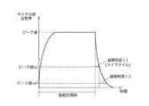
- FIG. 1B is a diagram showing a time change of the reflectance of the microwave obtained by the measuring apparatus shown in FIG. 1A.
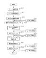
- FIG. 2 is a flowchart showing an example of the procedure of the TFT manufacturing process and the measurement timing by the microwave photoconductive decay method.
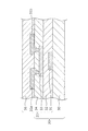
- FIG. 3 is a diagram showing a laminated structure of TFTs completed by the manufacturing process shown in FIG.
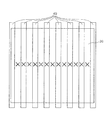
- FIG. 4 is a diagram showing measurement points on the panel by the microwave photoconductive decay method.
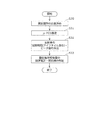
- FIG. 5 is a flowchart showing the procedure of the TFT evaluation method.
- FIG. 1B is a diagram showing a time change of the reflectance of the microwave obtained by the measuring apparatus shown in FIG. 1A.
- FIG. 2 is a flowchart showing an example of the procedure of the TFT manufacturing process and the measurement timing by the microwave photoconductive decay method.
- FIG. 3 is
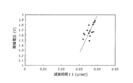
- FIG. 6A is a diagram illustrating an example of a measurement result related to a threshold voltage (a relationship between a reflectance decay time ⁇ 1 and a threshold voltage of an oxide semiconductor layer).
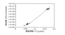
- FIG. 6B is a diagram illustrating another example of the measurement result related to the threshold voltage (relationship between the reflectance decay time ⁇ 2 and the threshold voltage of the oxide semiconductor layer).
- FIG. 7A is a diagram illustrating an example of a measurement result related to a resistance value (a relationship between a reflectance decay time ⁇ 1 and a resistance value of an oxide semiconductor layer).
- FIG. 7B is a diagram illustrating another example of the measurement result regarding the resistance value (relationship between the reflectance decay time ⁇ 2 and the resistance value of the oxide semiconductor layer).
- FIG. 7C is a diagram illustrating another example of the measurement result regarding the resistance value (relationship between the peak value of the reflectance and the resistance value of the oxide semiconductor layer).
- FIG. 8A is a diagram illustrating an example of positioning a measurement location depending on the position of the sputter target.
- FIG. 8B is a diagram illustrating another positioning example of the measurement location depending on the position of the sputter target.
- FIG. 9A is a diagram illustrating an example of positioning of measurement points depending on the film thickness and / or film quality of an oxide semiconductor layer.
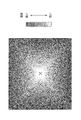
- FIG. 9B is a diagram illustrating an example of positioning a measurement location depending on the temperature distribution in the annealing process.
- a thin film transistor evaluation method is an evaluation method of a thin film transistor formed over a substrate as a threshold voltage evaluation, and the thin film transistor includes at least an oxide semiconductor layer functioning as a channel layer and the oxide A channel protective layer formed above the semiconductor layer, and the evaluation method is configured to reflect the reflectance of the microwave irradiated to the oxide semiconductor layer when the oxide semiconductor layer is pulsed with excitation light.
- An attenuation time which is a time required for the reflectance to attenuate from the first value to the second value, is calculated from the measurement step for measuring the change in the reflectance and the change in the reflectance obtained in the measurement step.
- the oxide semiconductor TFT having a channel protective layer and its intermediate product are not subjected to non-contact measurement by the microwave photoconductive decay method, but the oxide semiconductor thin film is not intended for a single oxide semiconductor thin film.
- the threshold voltage of the layer can be determined. Therefore, by incorporating such an evaluation step into an oxide semiconductor TFT manufacturing step (such as a display panel mass production step), the quality of the oxide semiconductor layer in the manufacturing process can be managed.
- the decay time is the time required for the reflectance to decay from the peak value to 1 / e of the peak value, where e is the base of the natural logarithm, and the reflectance is 1 / e of the peak value.
- the determination regarding the threshold voltage may be at least one of specifying the threshold voltage and determining whether or not the threshold voltage is a value within a predetermined range. This makes it possible to calculate the threshold voltage of the oxide semiconductor layer and to determine whether the oxide semiconductor TFT is good or defective based on the threshold voltage.
- the threshold voltage of the oxide semiconductor layer corresponding to the attenuation time calculated in the calculation step is specified by referring to the relationship between the attenuation time calculated in advance and the threshold voltage. Also good. Thereby, the threshold voltage of an unknown oxide semiconductor layer is specified from the decay time obtained by measurement using the relationship between the decay time and the threshold voltage obtained in advance.
- the thin film transistor evaluation method is a thin film transistor evaluation method formed on a substrate, and the thin film transistor includes at least an oxide semiconductor layer functioning as a channel layer, and an upper portion of the oxide semiconductor layer. And the evaluation method measures a change in the reflectance of the microwave irradiated to the oxide semiconductor layer when the oxide semiconductor layer is pulsed with excitation light. And a change in the reflectance obtained in the measurement step, an attenuation time which is a time required for the reflectance to attenuate from the first value to the second value, or the reflectance A calculation step for calculating a peak value, and a determination regarding the resistance value of the oxide semiconductor layer based on the decay time or the peak value calculated in the calculation step. Cormorants and a determination step.
- the oxide semiconductor TFT having a channel protective layer and its intermediate product are not subjected to non-contact measurement by the microwave photoconductive decay method, but the oxide semiconductor thin film is not intended for a single oxide semiconductor thin film.
- the resistance value of the layer can be determined. Therefore, by incorporating such an evaluation step into an oxide semiconductor TFT manufacturing step (such as a display panel mass production step), the quality of the oxide semiconductor layer in the manufacturing process can be managed.
- the decay time is the time required for the reflectance to decay from the peak value to 1 / e of the peak value, where e is the base of the natural logarithm, and the reflectance is 1 / e of the peak value.
- the determination regarding the resistance value may be at least one of specifying the resistance value and determining whether or not the resistance value is a value within a predetermined range. This makes it possible to calculate the resistance value of the oxide semiconductor layer and to determine whether the oxide semiconductor TFT is good or defective based on the resistance value.
- the oxide semiconductor layer corresponding to the attenuation time or peak value calculated in the calculation step is referred to by referring to a relationship between the attenuation time or peak value calculated in advance and the resistance value.
- the resistance value may be specified.
- the resistance value of the unknown oxide semiconductor layer is specified using the relationship between the attenuation time or peak value obtained in advance and the resistance value from the attenuation time or peak value obtained by the measurement.
- the thin film transistor may be subjected to a first annealing process for stabilizing the channel protective layer after the formation of the channel protective layer, and the measurement step may be performed after the first annealing process. Good. Accordingly, it can be confirmed whether or not the electrical characteristics of the oxide semiconductor layer have changed due to the annealing treatment that is highly likely to change the physical properties of the oxide semiconductor, and to what extent.
- the thin film transistor further includes a source and drain electrode formed above the channel protective layer, and an interlayer insulating layer formed above the source and drain electrode, and the measuring step includes the step of It may be performed after the formation of the insulating layer. Accordingly, non-contact measurement by the microwave photoconductive decay method can be performed on the oxide semiconductor TFT including not only the channel protective layer but also the interlayer insulating layer to determine the electrical characteristics of the oxide semiconductor layer.
- the thin film transistor may be subjected to a second annealing process for stabilizing the interlayer insulating layer after the formation of the interlayer insulating layer, and the measuring step may be performed after the second annealing process. Good. Thereby, the electrical characteristics of the oxide semiconductor TFT when the final manufacturing process is completed can be evaluated.
- the method further includes a positioning step for changing a measurement target location in the measurement step, and the measurement in the measurement step, the calculation in the calculation step, and the determination in the determination step are the target locations changed in the positioning step. May be performed.
- the quality control of the entire panel can be performed by performing measurement, parameter calculation, and determination of electrical characteristics while sequentially changing the position of a plurality of locations on the plane.
- the oxide semiconductor layer is formed by a sputtering method that targets a plurality of strip-shaped regions arranged at regular intervals on the substrate.
- the plurality of strip-shaped layers are formed.
- the measurement target location may be changed so that the measurement in the measurement step is performed on each of the regions sandwiched between adjacent regions in the row of the plurality of strip-like regions.
- the thickness of the oxide semiconductor layer is increased, and the thickness of the oxide semiconductor layer is decreased.
- a plurality of target portions arranged with at least one tendency of deterioration of the film quality of the layer and improvement of the film quality of the oxide semiconductor layer may be sequentially switched.
- a plurality of target portions arranged in a sequence in which the temperature in the annealing process for the thin film transistor tends to increase or decrease as the measurement target portion is sequentially switched. May be. Thereby, changes and variations in the electrical characteristics of the oxide semiconductor layer depending on the temperature distribution in the annealing treatment can be evaluated.
- the microwave frequency may be 10 GHz or more, and the wavelength of the excitation light may be 500 nm or less.
- the present invention can also be realized as a method for manufacturing a thin film transistor.
- the manufacturing method includes a step of forming an oxide semiconductor layer functioning as a channel layer on a substrate, a step of forming a channel protective layer above the oxide semiconductor layer, and a step of executing the evaluation method. . This makes it possible to manage the film quality of the oxide semiconductor layer in the manufacturing process.
- the present invention can also be realized as a thin film transistor.
- the thin film transistor is, for example, a thin film transistor formed on a substrate, and includes an oxide semiconductor layer functioning as a channel layer and a channel protective layer formed above the oxide semiconductor layer.
- the specified threshold voltage is 1.5 to 1.9 V, or the resistance value is 10 9 to 10 11 ⁇ .
- FIG. 1A is a block diagram illustrating a configuration of a measurement apparatus 10 that performs the thin film transistor evaluation method according to the present embodiment.
- This measuring apparatus 10 non-contactly evaluates the oxide semiconductor constituting the channel layer of the TFT 21 at a plurality of timings (in-line inspection) in the manufacturing process of the TFT 21 by the microwave photoconductive decay method.
- the measuring apparatus 10 irradiates the oxide semiconductor layer formed on the substrate 30 with excitation light and microwave, and determines the intensity of the reflected wave from the sample of the microwave that changes due to the irradiation of the excitation light. To detect.
- the basic configuration of the measuring apparatus 10 is the same as that of Patent Document 1, but as described below, in order to enable the evaluation of the TFT 21 in each manufacturing process, Unique ingenuity has been added.
- the substrate 30 is a glass substrate or the like.
- the TFT 21 is an oxide semiconductor TFT (including intermediate products in each manufacturing process until completed as a TFT) formed so as to be two-dimensionally arranged on the surface of the substrate 30.
- the substrate 30 and the TFT 21 (including the intermediate product) formed thereon are collectively referred to as a panel 20.
- the panel 20 is a drive panel for, for example, an organic EL display, which is configured by two-dimensionally forming a plurality of TFTs 21 on a substrate 30.
- the panel 20 is not only for a single display panel but also for a plurality of displays (for example, 4 chamfer) panels are included.
- the measurement apparatus 10 includes a pulse laser 11, a microwave oscillator 12, a waveguide assembly 13, a mixer 14, a signal processing device 15, a computer 16, a stage controller 17, and an XY stage 18.
- the pulse laser 11 is a light source that outputs excitation light irradiated to the TFT 21, and has a wavelength of 500 nm or less (for example, a wavelength of 349 nm), a power of 1 nJ / pulse to 10 ⁇ J / pulse, a pulse width of 5 nsec, and a beam diameter.
- a semiconductor laser or the like that emits pulsed ultraviolet light of 1.5 mm as excitation light.
- the pulse width of the excitation light is 15 nsec.
- the time order may be the same as the decay times ⁇ 1 and ⁇ 2 described later, and the measurement accuracy is not sufficient. Absent.
- the pulse width is set to 5 nsec.
- the pulse energy is 1 ⁇ J / pulse.
- a power larger than 1 ⁇ J / pulse is used. Is desirable.
- the pulse energy is preferably 1 to 2 ⁇ J / pulse, and the best measurement accuracy is obtained when the pulse energy is about 1.45 ⁇ J / pulse.
- the microwave oscillator 12 is a signal source that outputs a microwave (electromagnetic wave) irradiated to the measurement site of the TFT 21.
- the microwave oscillator 12 is preferably a signal source that outputs a microwave having a frequency of 10 GHz or more. In the present embodiment, it is a Gunn diode having a frequency of 26 GHz.
- the waveguide assembly 13 has a function of irradiating the measurement site of the TFT 21 with the excitation light output from the pulse laser 11, and branches the microwave output from the microwave oscillator 12 to be output to the LO input terminal of the mixer 14 and the TFT 21.
- the assembly has a function of capturing the reflected wave of the microwave irradiated to the measurement site of the TFT 21 and guiding it to the RF input terminal of the mixer 14.
- This waveguide assembly 13 has a mirror, a condensing lens, and a waveguide (not shown) for irradiating the excitation light, and reflects the excitation light output from the pulse laser 11 by the mirror, thereby collecting the condensing lens.
- the waveguide assembly 13 includes a directional coupler, a magic T, and a waveguide (not shown) for the microwave irradiation and the detection of the reflected wave.
- the waveguide assembly 13 splits the microwave output from the microwave oscillator 12 into two by the directional coupler, and transmits one of the branched first microwaves to the magic T and the other second microwave. The wave is transmitted to the LO input terminal of the mixer 14.
- the first microwave transmitted to the magic T is branched into two by the magic T, and one of the branched first main microwaves is passed through the first waveguide to the measurement site of the TFT 21 (the portion including the excitation unit).
- the other first sub-microwave after branching is radiated to the vicinity of the measurement region of the TFT 21 (the portion not including the excitation portion by the excitation light) through the second waveguide.
- Supplement the reflected wave is transmitted from the magic T to the RF input terminal of the mixer 14.
- the mixer 14 outputs a detection signal by mixing the second microwave and the reflected wave difference signal from the waveguide assembly 13.
- This detection signal is a signal representing the intensity of the reflected wave difference signal (the intensity of the reflected wave of the first microwave applied to the TFT 21), and is taken into the signal processing device 15.
- the signal processing device 15 detects the peak value (maximum value) of the change in the intensity of the reflected wave difference signal detected by the mixer 14, and sends a detection result and a signal indicating the change in the intensity of the reflected wave difference signal to the computer 16. It is a device to transmit to. More specifically, the signal processing device 15 monitors the change of the reflected wave difference signal for a predetermined time using the timing signal input from the computer 16 as a trigger, and reflects the maximum value of the level of the reflected wave difference signal obtained during that time. It is detected as the peak value of the change in the intensity of the wave difference signal.
- the signal processing device 15 includes a delay circuit that performs a delay process on the reflected wave difference signal, and the signal after the delay process is a signal with a predetermined sampling period (2.5 nsec in the present embodiment).
- the intensity is sequentially detected, and the peak value of the intensity change of the reflected wave difference signal is detected from the change in the detected value.
- the signal processing device 15 outputs the peak value and the signal intensity of the sampled reflected wave difference signal to the computer 16.
- the computer 16 includes a CPU, a storage unit, an input / output interface, and the like, and executes various processes by the CPU executing predetermined programs. For example, the computer 16 outputs a timing signal indicating the output timing of the excitation light to the pulse laser 11 and the signal processing device 15, and the peak value of the reflected wave difference signal detected by the signal processing device 15 and the sampled signal are sampled.
- the reflected wave difference signal (time series data) is captured and recorded in the storage unit. The recorded peak value and reflected wave difference signal are used for the evaluation of the TFT 21.
- the stage controller 17 controls the positioning of the measurement site of the TFT 21 by controlling the driving of the XY stage 18 in accordance with a command from the computer 16.
- the XY stage 18 is a mechanism unit that moves the panel 20 placed thereon in the X and Y directions on the horizontal plane, and is controlled by the stage controller 17.
- a substrate holding part for fixing the panel 20 is placed between the XY stage 18 and the panel 20, and the panel 20 is placed thereon.
- FIG. 1B is a diagram showing a time change of the reflectance of the microwave obtained by the measurement apparatus 10 shown in FIG. 1A.
- the TFT 21 (or its intermediate product) on which the oxide semiconductor layer is formed is irradiated with excitation light and microwave, and the maximum value of the reflected wave from the oxide semiconductor layer that changes due to the excitation light irradiation. (“Peak value” in FIG.
- the excitation light irradiation is stopped, and the change in reflectance of the reflected wave after the stop is measured.
- the time required for the reflectance to decay from the peak value to 1 / e of the peak value (“e is the base of the natural logarithm) (“attenuation time ⁇ 1” in FIG. 1B)
- the reflectance is The time required to attenuate from 1 / e to 1 / e 2 of the peak value (“attenuation time ⁇ 2” in FIG. 1B) and the peak value of reflectance (“peak value” in FIG. 1B) are calculated and calculated. Based on the decay time and the peak value, the determination on the threshold voltage and the resistance value of the oxide semiconductor layer can be performed.
- the time ⁇ 1 required for the reflectance to decay from the peak value to 1 / e of the peak value is the carrier lifetime (carrier lifetime).
- the time required for the reflectance to attenuate from the peak value to 1 / e 2 of the peak value may be included as the attenuation time.
- the decay time calculated by the measurement apparatus 10 in the present embodiment is the time required for the reflectance to decay from the first value to the second value, and specifically, the natural logarithm base is reduced.
- e is set, the time required for the reflectance to attenuate from the peak value to 1 / e of the peak value, and the reflectance attenuates from 1 / e of the peak value to 1 / e 2 of the peak value. And at least one of the time required for the reflectance to decay from the peak value to 1 / e 2 of the peak value.
- the measurement principle of such microwave photoconductive decay method is as follows.
- the excitation light applied to the oxide semiconductor layer of the TFT 21 is absorbed by the oxide semiconductor layer and generates excess carriers.
- the disappearance rate also increases.
- the excess carrier density has a constant peak value.
- saturation occurs and the density of excess carriers maintains a constant value.However, when irradiation with excitation light is stopped, recombination and disappearance of excess carriers cause The excess carriers are decreased, and finally the value before the irradiation with the excitation light is restored.
- the microwave irradiated to the oxide semiconductor layer is reflected with a reflectance based on the resistivity determined by the free carrier density of the oxide semiconductor layer.
- the resistivity of the oxide semiconductor layer decreases, and accordingly, the reflectance of the microwave increases.
- the excitation light irradiation is stopped, the resistivity increases as the number of excess carriers decreases, and the reflectance of the microwave decreases.
- the intensity of the reflected wave of the microwave is affected by excess carriers generated in the measurement site by the excitation light irradiation, and the degree of the effect also depends on the degree of defects and the like in the measurement site.
- the intensity of the reflected wave of the microwave irradiated to the oxide semiconductor layer is attenuated after being temporarily increased by the excitation light irradiation, but the more defects such as the oxide semiconductor layer, the more the reflected wave
- the threshold voltage of the oxide semiconductor layer is proportional to the reflectance decay time.
- the resistance value of the oxide semiconductor layer has a positive correlation that increases as the peak value of the intensity of the reflected wave increases, and has a positive correlation that increases as the decay time of the reflectance increases. Therefore, using a plurality of samples with known electrical characteristics, the relationship between measured values and electrical characteristics (attenuation time and threshold voltage, attenuation time and resistance value, peak value and resistance value) is specified in advance. By referencing, the electrical characteristics (threshold voltage, resistance value) can be determined from the measured values obtained for the unknown sample. In addition, the determination is specification of electrical characteristics (threshold voltage, resistance value) and determination of whether the electrical characteristics (threshold voltage, resistance value) are values within a predetermined range (good product or defective product). Including at least one determination).
- FIG. 2 is a flowchart showing an example of the manufacturing process procedure of the TFT 21 according to the present embodiment and the timing of measurement by the microwave photoconductive decay method (hereinafter also referred to as “ ⁇ -PCD measurement”).
- FIG. 3 is a view showing a laminated structure of the TFT 21 completed by such a manufacturing process.
- the gate electrode 31 is formed on the substrate 30 (S10).
- a glass substrate is prepared as the substrate 30, and a metal film in which a Mo film and a Cu film are sequentially stacked on the substrate 30 is formed by a sputtering method.
- the gate electrode 31 is formed by patterning the metal film by photolithography and wet etching.
- the film thickness of the gate electrode 31 is, for example, 20 to 500 nm.
- a gate insulating layer 32 is formed on the substrate 30 so as to cover the gate electrode 31 (S11).
- the gate insulating layer 32 is formed by forming a silicon oxide film or a silicon nitride film on the substrate 30 on which the gate electrode 31 is formed by a plasma CVD method.
- the film thickness of the gate insulating layer 32 is, for example, 50 to 300 nm.
- an oxide semiconductor layer is formed on the gate insulating layer 32 (S12).
- the film thickness of the oxide semiconductor layer is, for example, 20 to 200 nm.
- measurement is performed by the first microwave photoconductive decay method (S21). This is for checking whether an oxide semiconductor layer having desired electric characteristics is formed.
- the oxide semiconductor layer 33 constituting the channel layer of each TFT 21 is formed by patterning the formed oxide semiconductor layer by photolithography and wet etching (S13). Note that in this specification, with respect to the manufacture of an oxide semiconductor layer, the preparation of an oxide semiconductor layer that forms a channel layer of each TFT is referred to as “formation”, and the oxide semiconductor before being patterned for each TFT The production of the layer is called “film formation”.
- a channel protective layer 34 is formed on the gate insulating layer 32 so as to cover the oxide semiconductor layer 33 (S14).
- the channel protective layer 34 is formed by forming a silicon oxide film on the gate insulating layer 32 and the oxide semiconductor layer 33 by plasma CVD.
- the film thickness of the channel protective layer 34 is, for example, 50 to 500 nm.
- the second microwave photoconductive decay method (S22). This is to confirm whether the oxide semiconductor layer 33 is not damaged by the formation of the channel protective layer 34 and whether the electrical characteristics of the oxide semiconductor layer 33 are changed before and after the subsequent annealing treatment. .
- an annealing process (an example of a first annealing process) is performed in order to improve the stability of the electrical characteristics (threshold voltage shift or the like) of the oxide semiconductor layer 33 (S15).
- the panel 20 (intermediate product) manufactured so far is annealed at 250 ° C. to 400 ° C. for about 1 hour using an annealing apparatus.
- measurement is performed by the third microwave photoconductive decay method (S23). This is for checking whether or not the electrical characteristics of the oxide semiconductor layer 33 are changed by the annealing treatment.
- a source electrode 35a and a drain electrode 35b are formed on the channel protection layer 34 with a space therebetween (S16). Specifically, first, the channel protective layer 34 is etched by photolithography and dry etching, so that contact holes are opened over the regions functioning as the source region and the drain region of the oxide semiconductor layer 33. Then, a metal film in which a Mo film, a Cu film, and a CuMn film are sequentially deposited is formed in the contact hole and on the channel protective layer 34 by sputtering, and the metal film is patterned by photolithography and wet etching, A source electrode 35a and a drain electrode 35b are formed. The film thickness of the source electrode 35a and the drain electrode 35b is, for example, 100 to 500 nm.
- an interlayer insulating layer 36 is formed on the channel protective layer 34 so as to cover the source electrode 35a and the drain electrode 35b (S17).
- the interlayer insulating layer 36 is formed by forming a silicon oxide film on the source electrode 35a, the drain electrode 35b, and the channel protective layer 34 by plasma CVD.
- the film thickness of the interlayer insulating layer 36 is, for example, 50 to 1000 nm.
- measurement is performed by the fourth microwave photoconductive decay method (S24). This is to confirm whether or not the oxide semiconductor layer 33 is damaged due to the formation of the interlayer insulating layer 36 and whether or not the electrical characteristics of the oxide semiconductor layer 33 are changed before and after the subsequent annealing treatment. .
- an annealing process (an example of a second annealing process) is performed (S18).
- the panel 20 is annealed at 250 ° C. to 400 ° C. for about 1 hour using an annealing apparatus.
- measurement is performed by the fifth microwave photoconductive decay method (S25). This is for checking whether or not the electrical characteristics of the oxide semiconductor layer 33 are changed by the annealing treatment.
- in-line and non-contact measurement is performed by a total of five times by the microwave photoconductive decay method, the oxide semiconductor layer immediately after film formation is in the subsequent manufacturing process. It is possible to evaluate whether the electrical characteristics have changed due to damage or the like.
- a total of five measurement timings are illustrated after the oxide semiconductor layer is formed and before and after the subsequent two annealing treatments.
- the measurement timing is limited to such measurement timings. It is not a thing. After the oxide semiconductor layer is formed, measurement may be performed for each manufacturing process, or measurement after the manufacturing process, which is expected to cause little damage to the oxide semiconductor layer, may be omitted. .
- FIG. 4 is a diagram showing measurement points on the panel 20 by the microwave photoconductive decay method in the present embodiment.
- the vertical line and horizontal line (“GM / SD electrode line” in the figure) drawn on the panel 20 form a gate electrode 31, a source electrode 35a, a drain electrode 35b, and wirings connected to them. Indicates the location to be done.
- Measurement by the microwave photoconductive decay method is not performed on the electrode formation region 20a, which is a region where the gate electrode 31, the source electrode 35a and the drain electrode 35b are formed, but on the electrode where the gate electrode 31, the source electrode 35a and the drain electrode 35b are not formed. This is preferably performed on the formation region 20b. This is due to the following reasons.
- the electrode formation region 20a is a region where all the components constituting the TFT 21 shown in FIG. 3 are formed.
- the substrate 30, the gate electrode 31, the gate insulating layer 32, the oxide semiconductor layer 33, and the channel protective layer 34 are formed.
- the source electrode 35a, the drain electrode 35b, and the interlayer insulating layer 36 are deposited.
- the electrode non-forming region 20b is a region formed simultaneously with the electrode forming region 20a.
- the gate electrode 31, the source electrode 35a, and the drain electrode 35b are This is a region where the substrate 30, the gate insulating layer 32, the oxide semiconductor layer 33, the channel protective layer 34, and the interlayer insulating layer 36 are deposited.
- the microwave photoconductive decay method is a technique for measuring how the reflectance of microwaves changes depending on the resistivity determined by the free carrier density in the sample before and after irradiation with excitation light. If a conductive material such as metal or ITO (Indium Tin Oxide) is deposited as in 20a, the free carrier density is sufficiently high before the excitation light irradiation, so there is not much excess carrier even when the excitation light is irradiated. It is not excited, and as a result, the reflectance of the microwave does not change much. Therefore, it is considered difficult to calculate the decay time, peak value, etc. in the microwave photoconductive decay method.
- a conductive material such as metal or ITO (Indium Tin Oxide)
- the oxide semiconductor layer 33 constituting the TFT 21 can be evaluated by performing measurement by the microwave photoconductive decay method on the oxide semiconductor layer 33 in the electrode non-formation region 20b.
- any region in the panel 20 may be used as a measurement region by the microwave photoconductive decay method as long as it is a region where a conductive material such as metal or ITO is not deposited.
- the region is oxidized in the TFT 21 manufacturing process. It is desirable to select a region where the film thickness and film quality of the physical semiconductor layer 33 can change.
- FIG. 5 is a flowchart showing the procedure of the TFT evaluation method in the present embodiment.
- FIG. 5 shows the control procedure and processing by the computer 16 of the measuring apparatus 10 shown in FIG. 1A.
- the measurement location is positioned (positioning step S30).
- positioning for changing the measurement target point is performed.
- the computer 16 moves the XY stage 18 by giving a command to the stage controller 17 so that measurement by a microwave photoconductive decay method is performed on a desired measurement portion of the oxide semiconductor layer 33.
- measurement step S31 measurement by microwave photoconductive decay method ( ⁇ -PCD measurement) is performed (measurement step S31). That is, the change in the reflectance of the microwave irradiated to the oxide semiconductor layer 33 when the oxide semiconductor layer 33 to be measured is irradiated with a pulse of excitation light is measured.
- the computer 16 outputs a timing signal indicating the output timing of the excitation light to the pulse laser 11 and the signal processing device 15, and the peak value of the reflected wave difference signal detected by the signal processing device 15 and The sampled reflected wave difference signal is captured and recorded in the storage unit.
- At least one of the reflectance decay time and the peak value is calculated from the measurement result in the measurement step S31 (calculation step S32). That is, from the change in reflectance obtained in the measurement step S31, the time required for the reflectance to decay from the peak value to 1 / e of the peak value (lifetime) or the reflectance peaks from 1 / e of the peak value. At least one of an attenuation time which is a time required for attenuation to 1 / e 2 of the value and a peak value of the reflectance is calculated.
- the computer 16 takes the peak value of the reflected wave difference signal from the peak value of the reflected wave difference signal and the time series data of the reflected wave difference signal, which is acquired from the signal processing device 15 and recorded in the storage unit, from the reflectance.
- the decay time is the time required for the reflectivity to decay from the peak value to 1 / e of the peak value and the reflectivity from 1 / e of the peak value to 1 / e 2 of the peak value Is calculated.
- the decay time the time required for the reflectance to decay from the peak value to 1 / e 2 of the peak value may be used.
- the decay time calculated in the calculation step S32 is the time required for the reflectance to decay from the first value to the second value.
- the time required for the reflectivity to decay from a peak value to 1 / e of the peak value the time required for the reflectivity to decay from 1 / e of the peak value to 1 / e 2 of the peak value, and , At least one of the time required for the reflectance to attenuate from the peak value to 1 / e 2 of the peak value.
- the computer 16 makes a determination regarding at least one of the threshold voltage and the resistance value of the oxide semiconductor layer 33 (determination step S33). For example, in the determination regarding the threshold voltage, at least one of specifying the threshold voltage and determining whether or not the threshold voltage is a value within a predetermined range (including determination of a non-defective product or a defective product) is performed. For this purpose, the relationship between the decay time and the threshold voltage is specified in advance using a plurality of samples with known electrical characteristics, and the relationship is referred to so that the decay time obtained for an unknown sample can be used. Thus, the threshold voltage of the oxide semiconductor layer 33 can be determined.
- the determination regarding the resistance value at least one of specifying the resistance value and determining whether or not the resistance value is within a predetermined range (including determination of a non-defective product or a defective product) is performed.
- the relationship between the decay time or peak value and the resistance value is specified in advance using a plurality of samples having known electrical characteristics, and the attenuation obtained for an unknown sample is referred to by referring to the relationship.
- the resistance value of the oxide semiconductor layer 33 can be determined based on the time or the peak value.
- the decay time and peak value of the reflectance are calculated, and the electrical characteristics of both the threshold voltage and the resistance value of the oxide semiconductor layer are determined based on them.
- calculate at least one parameter either one of the two decay times or peak value
- calculate at least one electrical characteristic may be determined.
- the TFTs to be measured are as follows.
- the etching process for forming the gate electrode 31 is performed at the measurement location by the microwave photoconductive decay method, and the gate electrode material is etched.
- an amorphous oxide semiconductor layer (InGaZnO) was formed under the following conditions.
- composition of sputtering target InGaZnO 4
- Substrate temperature room temperature
- Oxide semiconductor layer thickness 60 nm
- Oxygen addition amount: O 2 / (Ar + O 2 ) 5%
- the electrode material was etched at the measurement site by the microwave photoconductive decay method, and only the channel protective layer 34 and the interlayer insulating layer 36 were laminated. That is, evaluation by the microwave photoconductive decay method was performed after each step in a state where the conductive material was not laminated.
- the measurement conditions (conditions of excitation light by the laser) by the microwave photoconductive decay method are as follows.
- Pulse width 5nsec Pulse energy: 1nJ / pulse-10 ⁇ J / pulse Beam diameter: 1.5mm ⁇
- the measurement results obtained by the microwave photoconductive decay method obtained under the above measurement conditions are as shown in FIGS. 6A, 6B, 7A, 7B, and 7C.
- electrical characteristics of a TEG (Test Element Group; evaluation element) whose electrical characteristics arranged in the vicinity of the measurement location are known in advance and measurement results obtained by the microwave photoconductive decay method are shown.
- FIG. 6A shows measurement results obtained by performing measurement using a microwave photoconductive decay method on a plurality of TFTs whose oxide semiconductor layer threshold voltages are known (the reflectance decay time ⁇ 1 and the threshold voltage of the oxide semiconductor layer).
- FIG. The decay time ⁇ 1 is the time (lifetime) required for the reflectance to decay from the peak value to 1 / e of the peak value.
- FIG. 6B shows measurement results obtained by performing measurement using a microwave photoconductive attenuation method on a plurality of TFTs whose threshold voltages of the oxide semiconductor layer are known (the reflectance decay time ⁇ 2 and the threshold voltage of the oxide semiconductor layer).
- FIG. The decay time ⁇ 2 is the time required for the reflectance to decay from 1 / e of the peak value to 1 / e 2 of the peak value.
- the reflectance decay time ⁇ 1 is proportional to the threshold voltage of the oxide semiconductor layer.
- the reflectance decay time ⁇ 2 is proportional to the threshold voltage of the oxide semiconductor layer.
- the decay time ⁇ 2 is about 10 times larger than the decay time ⁇ 1, and is distributed over a wide time range. Therefore, it can be said that the decay time ⁇ 2 is more dependent on the threshold voltage than the decay time ⁇ 1, and is excellent as a parameter used for evaluating the threshold voltage.
- the threshold voltage of the oxide semiconductor layer depends on the carrier trap level density in the oxide semiconductor layer or at the interface.
- the microwave photoconductive decay method is a method for evaluating the process in which excess carriers excited in an oxide semiconductor layer are recombined and attenuated at trap levels and the like. From the oxide semiconductor layer after irradiation with excitation light, The attenuation of the intensity of the reflected wave greatly depends on the trap level density in the oxide semiconductor layer or at the interface. Therefore, it is estimated that the threshold voltage of the oxide semiconductor layer and the decay time of the reflectance are positively correlated, more specifically, proportional.
- the threshold voltage of the oxide semiconductor layer varies depending not only on the oxide semiconductor layer but also on the influence of hydrogen diffusion from the gate insulating layer, the channel protective layer, and the interlayer insulating layer.
- the evaluation in Patent Document 1 is an evaluation by a microwave photoconductive decay method for an oxide semiconductor thin film formed on the surface of a glass substrate, and in the sample structure, carrier mobility as an oxide semiconductor thin film alone can be evaluated. However, it is not suitable for quantitative evaluation of the threshold voltage determined in the actual TFT structure which is a laminated structure.
- FIG. 7A shows measurement results obtained by performing measurement using a microwave photoconductive decay method on a plurality of TFTs whose resistance values of the oxide semiconductor layer are known (the reflectance decay time ⁇ 1 and the resistance value of the oxide semiconductor layer).
- FIG. 7B shows measurement results obtained by performing measurement using a microwave photoconductive decay method on a plurality of TFTs whose resistance values of the oxide semiconductor layer are known (the reflectance decay time ⁇ 2 and the resistance value of the oxide semiconductor layer).
- FIG. FIG. 7C shows measurement results obtained by performing microwave photoconductive decay measurement on a plurality of TFTs whose resistance values of the oxide semiconductor layer are known (the reflectance peak value and the resistance value of the oxide semiconductor layer).
- sheet resistance (Ohm / Sheet) is plotted as an example of the resistance value.
- the “resistance value” is a resistance value in a broad sense, and the resistance, sheet resistance, and the resistance when the film thickness, width, and length of the oxide semiconductor layer are fixed under a certain condition. It means to include resistivity.
- the resistance value of the oxide semiconductor and the decay times ⁇ 1 and ⁇ 2 of the reflectance have a positive correlation that the decay times ⁇ 1 and ⁇ 2 increase as the resistance value increases.
- the resistance value of the oxide semiconductor and the peak value of the reflectance have a positive correlation that the peak value increases as the resistance value increases.
- a sample having a resistance value distributed between 10 9 to 10 11 ⁇ is a sample that operates normally as a TFT, but a sample having a resistance value distributed from 10 3 to 10 5 ⁇ is a TFT. It is a sample that does not operate normally.
- the reason why the correlation shown in FIG. 7C is obtained with respect to the peak value of the reflectance and the resistance value of the oxide semiconductor layer is considered as follows. That is, the reflectance of the microwave increases as the resistivity determined by the density of free carriers decreases as described above. However, the graph shown in FIG. 7C shows the result that the peak value of the reflectance decreases as the resistance value decreases. This is because the peak value obtained by the measuring apparatus 10 does not indicate a simple reflectance, but a change in reflectance before and after the excitation light irradiation is observed (differential detection is performed). is there.
- the reflectance when the resistance value is low (that is, the density of free carriers is high), since there are already a large number of free carriers, the reflectance itself is high without irradiating the excitation light, but the excitation light Since the absolute number of excess carriers that can be excited when irradiating is reduced, the reflectance does not change much even when the excitation light is irradiated. As a result, the peak value obtained as the differential detection is a low value.
- the resistance value of the oxide semiconductor layer can be evaluated even when the channel protective layer or the interlayer insulating layer is stacked.
- the influence of the process on the resistance value of the oxide semiconductor layer can be evaluated non-destructively and non-contactly.
- an example of the threshold voltage of a sample that normally operates as a TFT is 1.5 to 1.9V.
- An example of the resistance value is 10 9 to 10 11 ⁇ . Therefore, an example of a TFT that is determined to be non-defective by the method for evaluating an oxide semiconductor TFT in this embodiment includes an oxide semiconductor layer that functions as a channel layer, and a channel protective layer that is formed above the oxide semiconductor layer.
- the threshold voltage specified by the evaluation method is 1.5 to 1.9 V, or the resistance value is 10 9 to 10 11 ⁇ .
- the oxide semiconductor thin film is not intended for a single oxide semiconductor thin film, but the oxide semiconductor TFT is subjected to the decay time and the peak value of the reflectance of the microwave.
- the electrical characteristics of the layer threshold voltage and resistance can be evaluated.
- One of the factors that enabled such measurement is that the pulse width of the excitation light applied to the oxide semiconductor TFT is short.
- the pulse width of the excitation light is 15 nsec.
- the pulse width of the excitation light is 5 nsec.
- the decay time in the microwave photoconductive decay method is very short on the order of psec, but the decay times ⁇ 1 and ⁇ 2 of the amorphous oxide semiconductor layer are generally several times, respectively. 10 nsec to several hundred nsec, and several tens nsec to several ⁇ sec.
- the pulse width of the excitation light is set to 15 nsec, the time order may be the same as the decay times ⁇ 1 and ⁇ 2 obtained by actual measurement, and the measurement accuracy may not be sufficient. Therefore, it is considered that the pulse width of the excitation light is preferably several nsec or less.
- FIG. 8A and FIG. 8B are diagrams showing an example of a measurement target location by the microwave photoconductive decay method in this embodiment. It is a figure which shows the example of positioning of the measurement location depending on the position of the sputter target for film-forming.
- a measurement location (location indicated by X) to be switched is shown.
- 8A shows an example of a measurement location when the sputter target is a cylindrical target
- FIG. 8B shows an example of a measurement location when the sputter target is a planar target.
- the oxide semiconductor layer is formed on the substrate 30 by sputtering using a plurality of strip-shaped regions arranged at regular intervals as targets. Accordingly, in the positioning step S30, measurement, parameter calculation, and determination are performed for each of the plurality of strip-shaped regions and the region sandwiched between adjacent regions in the arrangement of the plurality of strip-shaped regions. The measurement target locations by the microwave photoconductive decay method are sequentially changed so that steps S31 to S33) of FIG. 5 are performed. Thus, changes and variations in the electrical characteristics of the oxide semiconductor layer depending on the position of the sputtering target can be evaluated.
- FIG. 9A is a diagram showing an example of a measurement target location by the microwave photoconductive decay method in this embodiment. It is a figure which shows the example of positioning of the measurement location depending on the film thickness and / or film quality of an oxide semiconductor layer.
- the state (distribution) in which the film thickness (or film quality) of the oxide semiconductor layer gradually changes depending on the position, and the measurement points (locations indicated by X) that are sequentially switched are shown. Yes.
- FIG. 9A it is shown that the thicker the portion (or the poorer the film quality), the higher the concentration.
- the thickness of the oxide semiconductor layer is increased and the thickness of the oxide semiconductor layer is decreased as the measurement target portion.
- the measurement target location by the microwave photoconductive decay method is sequentially changed.
- the measurement location depending on the thickness and / or film quality of the oxide semiconductor layer as described above is determined depending on the thickness and / or film quality of the gate insulating layer, channel protective layer, or interlayer insulating layer.
- the positioning may be performed in the same manner as in the above positioning example. Accordingly, changes and variations in the electrical characteristics of the oxide semiconductor layer depending on the thickness and / or film quality of the gate insulating layer, the channel protective layer, or the interlayer insulating layer can be evaluated.
- FIG. 9B is a diagram showing an example of a measurement target location by the microwave photoconductive decay method in the present embodiment, and in particular, the temperature distribution in the annealing treatment. It is a figure which shows the example of positioning of the measurement location depending on.
- the planar temperature distribution of the panel 20 in the annealing treatments S15 and S18 of FIG. 2 and the measurement locations (locations indicated by X) to be sequentially switched are shown.
- the higher the density the higher the temperature.
- the temperature in the annealing process for the thin film transistor is increased or decreased with respect to a plurality of target portions arranged with a tendency to decrease.
- the measurement target location by the microwave photoconductive decay method is sequentially changed. Thereby, changes and variations in the electrical characteristics of the oxide semiconductor layer depending on the temperature distribution in the annealing treatment can be evaluated.
- the oxide semiconductor thin film including the channel protective layer and the interlayer insulating layer and the intermediate generation thereof are not intended for the oxide semiconductor thin film alone.
- the electrical characteristics such as the threshold voltage and the resistance value of the oxide semiconductor layer can be evaluated from an object in a non-contact manner from the decay time and peak value of the reflectance of the microwave. Therefore, since the measurement by the microwave photoconductive decay method can be incorporated into the manufacturing process of the oxide semiconductor TFT (that is, the panel mass production process), the oxide semiconductor TFT can be evaluated. And quality control can be performed in parallel.
- the evaluation method, the manufacturing method, and the thin film transistor of the thin film transistor of the present invention have been described based on the embodiment.
- the present invention is not limited to this embodiment. Unless it deviates from the meaning of this invention, the form which carried out the various deformation
- the measurement timing in the manufacture of the thin film transistor is not limited to the timing shown in FIG. 2, and at least once by the microwave photoconductive decay method after the oxide semiconductor layer is formed. Measurement only needs to be performed. By performing the measurement at least once in the manufacturing process, it is possible to evaluate the variation in quality of the oxide semiconductor layer depending on the planar position of the panel 20 and the difference from the quality of other panels.
- the threshold voltage and the resistance value are determined as the TFT evaluation method.
- other characteristics such as carrier mobility, S value (subthreshold characteristic), and reflectance attenuation curve are used. Calculation and determination of a fitting parameter or the like when is represented by an approximate curve may also be performed.
- the present invention can be used as an evaluation method and manufacturing method of a TFT having an oxide semiconductor layer, for example, as a non-contact TFT evaluation method by a microwave photoconductive decay method incorporated in a mass production process of a display panel.
Landscapes
- Physics & Mathematics (AREA)
- General Physics & Mathematics (AREA)
- Health & Medical Sciences (AREA)
- Electromagnetism (AREA)
- Toxicology (AREA)
- Engineering & Computer Science (AREA)
- Microelectronics & Electronic Packaging (AREA)
- Thin Film Transistor (AREA)
- Testing Or Measuring Of Semiconductors Or The Like (AREA)
Abstract
Description
本発明に係る薄膜トランジスタの評価方法は、閾値電圧の評価として、基板上に形成された薄膜トランジスタの評価方法であって、前記薄膜トランジスタは、少なくとも、チャネル層として機能する酸化物半導体層と、前記酸化物半導体層の上方に形成されたチャネル保護層とを有し、前記評価方法は、前記酸化物半導体層に励起光をパルス照射した場合における前記酸化物半導体層に照射しているマイクロ波の反射率の変化を測定する測定ステップと、前記測定ステップで得られた前記反射率の変化から、前記反射率が第1の値から第2の値に減衰するのに要する時間である減衰時間を算出する算出ステップと、前記算出ステップで算出された減衰時間に基づいて、前記酸化物半導体層の閾値電圧に関する判定を行う判定ステップとを含む。これにより、酸化物半導体薄膜単体を対象とするのではなく、チャネル保護層を有する酸化物半導体TFT及びその中間生成物に対して、マイクロ波光導電減衰法による非接触な測定を行って酸化物半導体層の閾値電圧を判定できる。よって、このような評価工程を酸化物半導体TFTの製造工程(ディスプレイパネルの量産工程等)に組み入れることで、製造プロセスにおける酸化物半導体層の膜質の管理が可能になる。
以下、本発明に係る薄膜トランジスタの評価方法、製造方法、及び、薄膜トランジスタの実施の形態について、図面を用いて詳細に説明する。なお、以下で説明する実施の形態は、いずれも本発明の好ましい一具体例を示すものである。以下の実施の形態で示される数値、形状、材料、構成要素、構成要素の配置位置及び接続形態、ステップ、ステップの順序等は、一例であり、本発明を限定する主旨ではない。また、以下の実施の形態における構成要素のうち、本発明の最上位概念を示す独立請求項に記載されていない構成要素については、より好ましい形態を構成する任意の構成要素として説明される。
基板温度:室温
酸化物半導体層の膜厚:60nm
酸素添加量:O2/(Ar+O2)=5%
パルス幅:5nsec
パルスエネルギー:1nJ/pulse~10μJ/pulse
ビーム径:1.5mmφ
20nsec<τ1<100nsec
80nsec<τ2<1500nsec
レーザ波長:349nm
パルス幅:5nsec
パルスエネルギー:1.45μJ/pulse
サンプリング間隔:2.5nsec
図8A及び図8Bは、本実施の形態におけるマイクロ波光導電減衰法による測定の対象箇所の一例を示す図であり、特に、酸化物半導体層を成膜するためのスパッタターゲットの位置に依存した測定箇所の位置決め例を示す図である。ここには、パネル20(あるいは、基板30)の位置と、図2に示される酸化物半導体層の成膜ステップS12でのスパッタリング法におけるターゲット(酸化物半導体スパッタターゲット40)の位置と、順次に切り替える対象となる測定箇所(Xで示される箇所)が示されている。なお、図8Aは、スパッタターゲットが円筒ターゲットである場合の測定箇所の例を示し、図8Bは、スパッタターゲットがプレーナターゲットである場合の測定箇所の例を示している。
図9Aは、本実施の形態におけるマイクロ波光導電減衰法による測定の対象箇所の一例を示す図であり、特に、酸化物半導体層の膜厚及び/又は膜質に依存した測定箇所の位置決め例を示す図である。ここには、酸化物半導体層の膜厚(又は、膜質)が位置によって徐々に変化していく様子(分布)と、順次に切り替える対象となる測定箇所(Xで示される箇所)が示されている。図9Aにおいて、濃度が濃い箇所ほど、膜厚が厚い(あるいは、膜質が悪い)ことを示している。
図9Bは、本実施の形態におけるマイクロ波光導電減衰法による測定の対象箇所の一例を示す図であり、特に、アニール処理における温度分布に依存した測定箇所の位置決め例を示す図である。ここには、図2のアニール処理S15及びS18におけるパネル20の平面的な温度分布と、順次に切り替える対象となる測定箇所(Xで示される箇所)が示されている。図9Bにおいて、濃度が濃い箇所ほど、温度が高いことを示している。
11 パルスレーザ
12 マイクロ波発振器
13 導波アセンブリ
14 ミキサ
15 信号処理装置
16 コンピュータ
17 ステージコントローラ
18 XYステージ
20 パネル
20a 電極形成領域
20b 電極非形成領域
21 TFT
30 基板
31 ゲート電極
32 ゲート絶縁層
33 酸化物半導体層
34 チャネル保護層
35a ソース電極
35b ドレイン電極
36 層間絶縁層
40 酸化物半導体スパッタターゲット
Claims (19)
- 基板上に形成された薄膜トランジスタの評価方法であって、
前記薄膜トランジスタは、少なくとも、チャネル層として機能する酸化物半導体層と、前記酸化物半導体層の上方に形成されたチャネル保護層とを有し、
前記評価方法は、
前記酸化物半導体層に励起光をパルス照射した場合における前記酸化物半導体層に照射しているマイクロ波の反射率の変化を測定する測定ステップと、
前記測定ステップで得られた前記反射率の変化から、前記反射率が第1の値から第2の値に減衰するのに要する時間である減衰時間を算出する算出ステップと、
前記算出ステップで算出された減衰時間に基づいて、前記酸化物半導体層の閾値電圧に関する判定を行う判定ステップと
を含む薄膜トランジスタの評価方法。 - 前記減衰時間は、自然対数の底をeとしたときに、
前記反射率がピーク値から前記ピーク値の1/eに減衰するのに要する時間、
前記反射率が前記ピーク値の1/eから前記ピーク値の1/e2に減衰するのに要する時間、又は、
前記反射率が前記ピーク値から前記ピーク値の1/e2に減衰するのに要する時間である
請求項1記載の薄膜トランジスタの評価方法。 - 前記閾値電圧に関する判定は、前記閾値電圧の特定、及び、前記閾値電圧が予め定められた範囲内の値であるか否かの判定の少なくとも一つである
請求項1又は2記載の薄膜トランジスタの評価方法。 - 前記判定ステップでは、予め算出された減衰時間と閾値電圧との関係を参照することで、前記算出ステップで算出された前記減衰時間に対応する前記酸化物半導体層の閾値電圧を特定する
請求項1~3のいずれか1項に記載の薄膜トランジスタの評価方法。 - 基板上に形成された薄膜トランジスタの評価方法であって、
前記薄膜トランジスタは、少なくとも、チャネル層として機能する酸化物半導体層と、前記酸化物半導体層の上方に形成されたチャネル保護層とを有し、
前記評価方法は、
前記酸化物半導体層に励起光をパルス照射した場合における前記酸化物半導体層に照射しているマイクロ波の反射率の変化を測定する測定ステップと、
前記測定ステップで得られた前記反射率の変化から、前記反射率が第1の値から第2の値に減衰するのに要する時間である減衰時間、又は、前記反射率のピーク値を算出する算出ステップと、
前記算出ステップで算出された減衰時間又はピーク値に基づいて、前記酸化物半導体層の抵抗値に関する判定を行う判定ステップと
を含む薄膜トランジスタの評価方法。 - 前記減衰時間は、自然対数の底をeとしたときに、
前記反射率がピーク値から前記ピーク値の1/eに減衰するのに要する時間、
前記反射率が前記ピーク値の1/eから前記ピーク値の1/e2に減衰するのに要する時間、又は、
前記反射率が前記ピーク値から前記ピーク値の1/e2に減衰するのに要する時間である
請求項5記載の薄膜トランジスタの評価方法。 - 前記抵抗値に関する判定は、前記抵抗値の特定、及び、前記抵抗値が予め定められた範囲内の値であるか否かの判定の少なくとも一つである
請求項5又は6記載の薄膜トランジスタの評価方法。 - 前記判定ステップでは、予め算出された減衰時間又はピーク値と抵抗値との関係を参照することで、前記算出ステップで算出された前記減衰時間又は前記ピーク値に対応する前記酸化物半導体層の抵抗値を特定する
請求項6又は7記載の薄膜トランジスタの評価方法。 - 前記薄膜トランジスタは、前記チャネル保護層の形成後に、前記チャネル保護層を安定化させるための第1のアニール処理が施され、
前記測定ステップは、前記第1のアニール処理の後に行われる
請求項1~8のいずれか1項に記載の薄膜トランジスタの評価方法。 - 前記薄膜トランジスタは、さらに、前記チャネル保護層の上方に形成されたソース及びドレイン電極と、前記ソース及びドレイン電極の上方に形成された層間絶縁層とを有し、
前記測定ステップは、前記層間絶縁層の形成後に行われる
請求項1~9のいずれか1項に記載の薄膜トランジスタの評価方法。 - 前記薄膜トランジスタは、前記層間絶縁層の形成後に、前記層間絶縁層を安定化させるための第2のアニール処理が施され、
前記測定ステップは、前記第2のアニール処理の後に行われる
請求項10記載の薄膜トランジスタの評価方法。 - さらに、前記測定ステップによる測定の対象箇所を変更する位置決めステップを含み、
前記測定ステップによる測定、前記算出ステップによる算出、及び、前記判定ステップにおける判定は、前記位置決めステップで変更された対象箇所に対して行われる
請求項1~11のいずれか1項に記載の薄膜トランジスタの評価方法。 - 前記酸化物半導体層は、前記基板上において、一定の間隔をおいて並ぶ複数の短冊状の領域をターゲットとするスパッタ法によって形成され、
前記位置決めステップでは、前記複数の短冊状の領域及び前記複数の短冊状の領域の並びにおける隣接した領域で挟まれる領域のそれぞれに対して、前記測定ステップによる測定が行われるように、前記測定の対象箇所を変更する
請求項12記載の薄膜トランジスタの評価方法。 - 前記位置決めステップでは、前記測定の対象箇所として、前記酸化物半導体層の膜厚が厚くなっていく、前記酸化物半導体層の膜厚が薄くなっていく、前記酸化物半導体層の膜質が悪くなっていく、及び、前記酸化物半導体層の膜質が良くなっていく、の少なくとも一つの傾向をもって並ぶ複数の対象箇所を順に切り替えていく
請求項12記載の薄膜トランジスタの評価方法。 - 前記位置決めステップでは、前記測定の対象箇所として、前記薄膜トランジスタに対するアニール処理における温度が高くなっていく、又は、低くなっていく傾向をもって並ぶ複数の対象箇所を順に切り替えていく
請求項12記載の薄膜トランジスタの評価方法。 - 前記マイクロ波の周波数は、10GHz以上である
請求項1~15のいずれか1項に記載の薄膜トランジスタの評価方法。 - 前記励起光の波長は、500nm以下である
請求項1~16のいずれか1項に記載の薄膜トランジスタの評価方法。 - 薄膜トランジスタの製造方法であって、
基板上にチャネル層として機能する酸化物半導体層を形成するステップと、
前記酸化物半導体層の上方にチャネル保護層を形成するステップと、
請求項1~8のいずれか1項に記載の評価方法を実行するステップと
を含む薄膜トランジスタの製造方法。 - 基板上に形成される薄膜トランジスタであって、
チャネル層として機能する酸化物半導体層と、
前記酸化物半導体層の上方に形成されたチャネル保護層とを備え、
請求項1~8のいずれか1項に記載の評価方法によって特定された閾値電圧が1.5~1.9V、又は、抵抗値が109~1011Ωである
薄膜トランジスタ。
Priority Applications (2)
| Application Number | Priority Date | Filing Date | Title |
|---|---|---|---|
| JP2015535295A JP6082950B2 (ja) | 2013-09-03 | 2014-06-25 | 薄膜トランジスタの評価方法、製造方法、及び、薄膜トランジスタ |
| US14/915,704 US10230003B2 (en) | 2013-09-03 | 2014-06-25 | Method of evaluating thin-film transistor, method of manufacturing thin-film transistor, and thin-film transistor |
Applications Claiming Priority (2)
| Application Number | Priority Date | Filing Date | Title |
|---|---|---|---|
| JP2013182256 | 2013-09-03 | ||
| JP2013-182256 | 2013-09-03 |
Publications (1)
| Publication Number | Publication Date |
|---|---|
| WO2015033499A1 true WO2015033499A1 (ja) | 2015-03-12 |
Family
ID=52628003
Family Applications (1)
| Application Number | Title | Priority Date | Filing Date |
|---|---|---|---|
| PCT/JP2014/003395 Ceased WO2015033499A1 (ja) | 2013-09-03 | 2014-06-25 | 薄膜トランジスタの評価方法、製造方法、及び、薄膜トランジスタ |
Country Status (3)
| Country | Link |
|---|---|
| US (1) | US10230003B2 (ja) |
| JP (1) | JP6082950B2 (ja) |
| WO (1) | WO2015033499A1 (ja) |
Cited By (5)
| Publication number | Priority date | Publication date | Assignee | Title |
|---|---|---|---|---|
| WO2016016776A1 (ja) * | 2014-07-31 | 2016-02-04 | 株式会社半導体エネルギー研究所 | 半導体装置、及び半導体装置の評価方法 |
| CN107234525A (zh) * | 2016-03-28 | 2017-10-10 | 株式会社迪思科 | 被加工物的评价方法 |
| WO2017188323A1 (ja) * | 2016-04-27 | 2017-11-02 | 株式会社神戸製鋼所 | 酸化物半導体薄膜の品質評価方法、及び前記酸化物半導体薄膜の品質管理方法、並びに該品質評価方法を用いる半導体の製造装置 |
| JP6250855B1 (ja) * | 2016-04-27 | 2017-12-20 | 株式会社神戸製鋼所 | 酸化物半導体薄膜の品質評価方法、及び前記酸化物半導体薄膜の品質管理方法、並びに該品質評価方法を用いる半導体の製造装置 |
| JP2023130112A (ja) * | 2022-03-07 | 2023-09-20 | 富士電機株式会社 | センサシステム及び気液比の測定方法 |
Families Citing this family (1)
| Publication number | Priority date | Publication date | Assignee | Title |
|---|---|---|---|---|
| CN114646856B (zh) * | 2022-03-18 | 2025-08-01 | 南京邮电大学 | 一种聚合物晶体管沟道界面评估方法 |
Citations (4)
| Publication number | Priority date | Publication date | Assignee | Title |
|---|---|---|---|---|
| JP2008177476A (ja) * | 2007-01-22 | 2008-07-31 | Sharp Corp | 半導体評価方法、半導体評価装置、半導体デバイス製造方法、および半導体デバイス製造装置 |
| JP2012033857A (ja) * | 2010-06-30 | 2012-02-16 | Kobe Steel Ltd | 酸化物半導体薄膜の評価方法、及び酸化物半導体薄膜の品質管理方法 |
| WO2012039099A1 (ja) * | 2010-09-22 | 2012-03-29 | 株式会社神戸製鋼所 | μ-PCD法を用いた薄膜半導体の結晶性評価装置 |
| JP2013030542A (ja) * | 2011-07-27 | 2013-02-07 | Panasonic Liquid Crystal Display Co Ltd | 非晶質半導体膜の評価方法、及び半導体装置の製造方法 |
Family Cites Families (7)
| Publication number | Priority date | Publication date | Assignee | Title |
|---|---|---|---|---|
| KR100213603B1 (ko) * | 1994-12-28 | 1999-08-02 | 가나이 쯔또무 | 전자회로기판의 배선수정방법 및 그 장치와 전자회로기판 |
| HU227170B1 (en) * | 2000-02-17 | 2010-09-28 | Semilab Felvezetoe Fiz Lab Rt | Surface passivation method and arrangement for measuring life time of minority carrier of semiconductors |
| US6534774B2 (en) * | 2000-09-08 | 2003-03-18 | Mitsubishi Materials Silicon Corporation | Method and apparatus for evaluating the quality of a semiconductor substrate |
| JP2008177387A (ja) * | 2007-01-19 | 2008-07-31 | Fujifilm Corp | 放射線画像検出装置 |
| JP5185357B2 (ja) | 2009-12-17 | 2013-04-17 | 株式会社半導体エネルギー研究所 | 半導体装置 |
| KR20120000499A (ko) | 2010-06-25 | 2012-01-02 | 가부시키가이샤 한도오따이 에네루기 켄큐쇼 | 트랜지스터 및 반도체 장치 |
| US9261609B2 (en) * | 2012-08-20 | 2016-02-16 | General Electric Company | Apparatus and methods for charge collection control in radiation detectors |
-
2014
- 2014-06-25 WO PCT/JP2014/003395 patent/WO2015033499A1/ja not_active Ceased
- 2014-06-25 JP JP2015535295A patent/JP6082950B2/ja active Active
- 2014-06-25 US US14/915,704 patent/US10230003B2/en active Active
Patent Citations (4)
| Publication number | Priority date | Publication date | Assignee | Title |
|---|---|---|---|---|
| JP2008177476A (ja) * | 2007-01-22 | 2008-07-31 | Sharp Corp | 半導体評価方法、半導体評価装置、半導体デバイス製造方法、および半導体デバイス製造装置 |
| JP2012033857A (ja) * | 2010-06-30 | 2012-02-16 | Kobe Steel Ltd | 酸化物半導体薄膜の評価方法、及び酸化物半導体薄膜の品質管理方法 |
| WO2012039099A1 (ja) * | 2010-09-22 | 2012-03-29 | 株式会社神戸製鋼所 | μ-PCD法を用いた薄膜半導体の結晶性評価装置 |
| JP2013030542A (ja) * | 2011-07-27 | 2013-02-07 | Panasonic Liquid Crystal Display Co Ltd | 非晶質半導体膜の評価方法、及び半導体装置の製造方法 |
Cited By (14)
| Publication number | Priority date | Publication date | Assignee | Title |
|---|---|---|---|---|
| WO2016016776A1 (ja) * | 2014-07-31 | 2016-02-04 | 株式会社半導体エネルギー研究所 | 半導体装置、及び半導体装置の評価方法 |
| JPWO2016016776A1 (ja) * | 2014-07-31 | 2017-07-27 | 株式会社半導体エネルギー研究所 | 半導体装置、及び半導体装置の評価方法 |
| CN107234525A (zh) * | 2016-03-28 | 2017-10-10 | 株式会社迪思科 | 被加工物的评价方法 |
| CN107234525B (zh) * | 2016-03-28 | 2021-01-12 | 株式会社迪思科 | 器件晶片的评价方法 |
| CN109155264A (zh) * | 2016-04-27 | 2019-01-04 | 株式会社神户制钢所 | 氧化物半导体薄膜的品质评价方法及上述氧化物半导体薄膜的品质管理方法以及使用该品质评价方法的半导体的制造装置 |
| KR20180126558A (ko) * | 2016-04-27 | 2018-11-27 | 가부시키가이샤 고베 세이코쇼 | 산화물 반도체 박막의 품질 평가 방법, 및 상기 산화물 반도체 박막의 품질 관리 방법, 그리고 해당 품질 평가 방법을 이용하는 반도체의 제조 장치 |
| JP6250855B1 (ja) * | 2016-04-27 | 2017-12-20 | 株式会社神戸製鋼所 | 酸化物半導体薄膜の品質評価方法、及び前記酸化物半導体薄膜の品質管理方法、並びに該品質評価方法を用いる半導体の製造装置 |
| TWI649819B (zh) * | 2016-04-27 | 2019-02-01 | 日商神戶製鋼所股份有限公司 | 氧化物半導體薄膜的品質評價方法、該氧化物半導體薄膜的品質管理方法以及使用該品質評價方法的半導體製造裝置 |
| US10475711B2 (en) | 2016-04-27 | 2019-11-12 | Kobe Steel, Ltd. | Method for evaluating quality of oxide semiconductor thin film, method for managing quality of oxide semiconductor thin film, and device for manufacturing semiconductor using said method for managing quality |
| KR102086442B1 (ko) | 2016-04-27 | 2020-03-09 | 가부시키가이샤 고베 세이코쇼 | 산화물 반도체 박막의 품질 평가 방법, 및 상기 산화물 반도체 박막의 품질 관리 방법, 그리고 해당 품질 평가 방법을 이용하는 반도체의 제조 장치 |
| WO2017188323A1 (ja) * | 2016-04-27 | 2017-11-02 | 株式会社神戸製鋼所 | 酸化物半導体薄膜の品質評価方法、及び前記酸化物半導体薄膜の品質管理方法、並びに該品質評価方法を用いる半導体の製造装置 |
| JP2023130112A (ja) * | 2022-03-07 | 2023-09-20 | 富士電機株式会社 | センサシステム及び気液比の測定方法 |
| JP7563409B2 (ja) | 2022-03-07 | 2024-10-08 | 富士電機株式会社 | センサシステム及び気液比の測定方法 |
| US12399136B2 (en) | 2022-03-07 | 2025-08-26 | Fuji Electric Co., Ltd. | Sensor system and method for measuring gas liquid ratio |
Also Published As
| Publication number | Publication date |
|---|---|
| JPWO2015033499A1 (ja) | 2017-03-02 |
| US10230003B2 (en) | 2019-03-12 |
| US20160197198A1 (en) | 2016-07-07 |
| JP6082950B2 (ja) | 2017-02-22 |
Similar Documents
| Publication | Publication Date | Title |
|---|---|---|
| JP6082950B2 (ja) | 薄膜トランジスタの評価方法、製造方法、及び、薄膜トランジスタ | |
| JP5798669B2 (ja) | 酸化物半導体薄膜の評価方法、及び酸化物半導体薄膜の品質管理方法、並びに上記評価方法に用いられる評価装置 | |
| JP5814558B2 (ja) | 酸化物半導体薄膜の評価方法、及び酸化物半導体薄膜の品質管理方法 | |
| KR101775803B1 (ko) | 산화물 반도체 박막의 평가 방법, 및 산화물 반도체 박막의 품질 관리 방법, 및 상기 평가 방법에 이용되는 평가 소자 및 평가 장치 | |
| TWI552233B (zh) | An oxide semiconductor thin film, and a thin film of the oxide semiconductor The quality evaluation method of the laminated body having the protective film on the surface of the film, and the quality management method of the oxide semiconductor thin film | |
| TWI652749B (zh) | A method for evaluating the quality of a laminate for evaluation of a thin film transistor, And quality management method of oxide semiconductor film | |
| TWI649819B (zh) | 氧化物半導體薄膜的品質評價方法、該氧化物半導體薄膜的品質管理方法以及使用該品質評價方法的半導體製造裝置 | |
| US9316589B2 (en) | Method for evaluating oxide semiconductor thin film, and method for quality control of oxide semiconductor thin film | |
| US8080434B2 (en) | Nondestructive testing method for oxide semiconductor layer and method for making oxide semiconductor layer | |
| KR101493163B1 (ko) | 박막 트랜지스터의 반도체층용 박막의 형성에 사용되는 타깃 조립체의 품질 평가 방법 | |
| JP6653217B2 (ja) | 酸化物半導体薄膜の表面に保護膜を有する積層体の品質評価方法、及び酸化物半導体薄膜の品質管理方法 | |
| JP5961314B2 (ja) | 酸化物半導体薄膜の膜質管理方法 | |
| JP2013030542A (ja) | 非晶質半導体膜の評価方法、及び半導体装置の製造方法 | |
| JP6250855B1 (ja) | 酸化物半導体薄膜の品質評価方法、及び前記酸化物半導体薄膜の品質管理方法、並びに該品質評価方法を用いる半導体の製造装置 | |
| JP7078525B2 (ja) | 薄膜トランジスタのストレス耐性の予測方法 |
Legal Events
| Date | Code | Title | Description |
|---|---|---|---|
| 121 | Ep: the epo has been informed by wipo that ep was designated in this application |
Ref document number: 14842047 Country of ref document: EP Kind code of ref document: A1 |
|
| ENP | Entry into the national phase |
Ref document number: 2015535295 Country of ref document: JP Kind code of ref document: A |
|
| WWE | Wipo information: entry into national phase |
Ref document number: 14915704 Country of ref document: US |
|
| NENP | Non-entry into the national phase |
Ref country code: DE |
|
| 122 | Ep: pct application non-entry in european phase |
Ref document number: 14842047 Country of ref document: EP Kind code of ref document: A1 |