WO2015030020A1 - 遮断素子、及び遮断素子回路 - Google Patents
遮断素子、及び遮断素子回路 Download PDFInfo
- Publication number
- WO2015030020A1 WO2015030020A1 PCT/JP2014/072348 JP2014072348W WO2015030020A1 WO 2015030020 A1 WO2015030020 A1 WO 2015030020A1 JP 2014072348 W JP2014072348 W JP 2014072348W WO 2015030020 A1 WO2015030020 A1 WO 2015030020A1
- Authority
- WO
- WIPO (PCT)
- Prior art keywords
- melting point
- soluble conductor
- point metal
- circuit
- conductor
- Prior art date
- Legal status (The legal status is an assumption and is not a legal conclusion. Google has not performed a legal analysis and makes no representation as to the accuracy of the status listed.)
- Ceased
Links
Images


Classifications
-
- H—ELECTRICITY
- H01—ELECTRIC ELEMENTS
- H01H—ELECTRIC SWITCHES; RELAYS; SELECTORS; EMERGENCY PROTECTIVE DEVICES
- H01H37/00—Thermally-actuated switches
- H01H37/74—Switches in which only the opening movement or only the closing movement of a contact is effected by heating or cooling
- H01H37/76—Contact member actuated by melting of fusible material, actuated due to burning of combustible material or due to explosion of explosive material
- H01H37/761—Contact member actuated by melting of fusible material, actuated due to burning of combustible material or due to explosion of explosive material with a fusible element forming part of the switched circuit
-
- H—ELECTRICITY
- H01—ELECTRIC ELEMENTS
- H01H—ELECTRIC SWITCHES; RELAYS; SELECTORS; EMERGENCY PROTECTIVE DEVICES
- H01H61/00—Electrothermal relays
- H01H61/02—Electrothermal relays wherein the thermally-sensitive member is heated indirectly, e.g. resistively, inductively
-
- H—ELECTRICITY
- H01—ELECTRIC ELEMENTS
- H01M—PROCESSES OR MEANS, e.g. BATTERIES, FOR THE DIRECT CONVERSION OF CHEMICAL ENERGY INTO ELECTRICAL ENERGY
- H01M50/00—Constructional details or processes of manufacture of the non-active parts of electrochemical cells other than fuel cells, e.g. hybrid cells
- H01M50/50—Current conducting connections for cells or batteries
- H01M50/572—Means for preventing undesired use or discharge
-
- H—ELECTRICITY
- H01—ELECTRIC ELEMENTS
- H01M—PROCESSES OR MEANS, e.g. BATTERIES, FOR THE DIRECT CONVERSION OF CHEMICAL ENERGY INTO ELECTRICAL ENERGY
- H01M2200/00—Safety devices for primary or secondary batteries
- H01M2200/20—Pressure-sensitive devices
Definitions
- the present invention relates to a shutoff element and a shutoff element circuit that ensure safety by electrically and physically shutting off a power supply line and a signal line.
- a battery pack incorporates a number of protection circuits such as overcharge protection and overdischarge protection, It has a function of shutting off the output of the battery pack in a predetermined case.
- Some types of this type of interruption element perform overcharge protection or overdischarge protection operation of the battery pack by turning on / off the output using an FET switch built in the battery pack.
- the FET switch is short-circuited for some reason, when a lightning surge or the like is applied and an instantaneous large current flows, the output voltage drops abnormally due to the life of the battery cell, or conversely an excessively abnormal voltage
- a shut-off element made of a fuse element having a function of shutting off the current path by an external signal is used. .
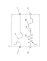
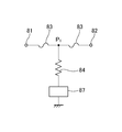
- the blocking element 80 of the protection circuit for such a lithium ion secondary battery or the like is soluble between the first and second electrodes 81 and 82 connected on the current path.
- a conductor 83 is connected to form part of the current path, and the fusible conductor 83 on the current path is self-heated due to overcurrent, or is melted by a heating element 84 provided inside the shut-off element 80. Yes.
- the blocking element 80 includes an insulating substrate 85, a heating element 84 stacked on the insulating substrate 85 and covered with an insulating member 86, and first and second electrodes 81 formed on both ends of the insulating substrate 85. , 82, a heating element extraction electrode 88 laminated on the insulating member 86 so as to overlap the heating element 84, both ends are connected to the first and second electrodes 81, 82, respectively, and the central portion is the heating element extraction A soluble conductor 83 connected to the electrode 88.
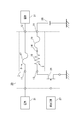
- FIG. 18 is a circuit diagram of the blocking element 80. That is, the interruption element 80 generates heat by melting the soluble conductor 83 by energizing the soluble conductor 83 connected in series via the heating element extraction electrode 88 and the connection point of the soluble conductor 83 to generate heat.
- This is a circuit configuration including the body 84.
- the soluble conductor 83 is connected in series on the charging / discharging electric current path
- the current control element 87 is composed of, for example, a field effect transistor (hereinafter referred to as FET), and when the lithium ion secondary battery exhibits an abnormal voltage, current flows through the heating element 84 via the soluble conductor 83. To be controlled.
- FET field effect transistor
- the interruption element 80 melts the soluble conductor 83 on the current path by the heat generation of the heating element 84 and collects the molten conductor on the heating element extraction electrode 88, whereby the first and second electrodes 81 and 82 are collected.
- the current path between them can be cut off, and the charge / discharge path of the battery pack can be cut off electrically and physically.
- the power for generating heat from the heating element 84 is supplied through the soluble conductor 83, but the first electrode 81 to the soluble conductor 83 to Since the current path over the second electrode 82 is a charging / discharging path of the battery, a sufficient amount of heat can be obtained to cause the heating element 84 to melt the soluble conductor 83 even when the heating element 84 is energized.
- the interruption element 80 when the interruption element 80 is used in a signal line through which a current weaker than that of the power supply line is used, the electric power sufficient to obtain a heat generation amount sufficient for fusing the soluble conductor 83 to the heating element 84 is supplied. Therefore, the use of the blocking element 80 is limited to the use of a large current.
- the current control element 87 that switches the current path to the heating element 84 side is required to improve the rating in the same manner as the current rating increases.
- a highly rated current control element is generally expensive and disadvantageous in terms of cost.
- the present invention can supply sufficient power for fusing a soluble conductor to a heating element even when incorporated in a weak current path, and can be used for any application, and
- An object is to provide a breaker circuit.
- a blocking element according to the present invention is formed on an insulating substrate, the first and second electrodes that are formed on the insulating substrate and constitute the first circuit, and the insulating substrate.
- the third to fifth electrodes constituting the second circuit, the first fusible conductor mounted between the first and second electrodes, and the third and fourth electrodes are connected.
- a heating element and a second fusible conductor mounted between the fourth and fifth electrodes, and a current is passed between the third to fifth electrodes to generate heat generated by the heating element, After the first soluble conductor is blown, the second soluble conductor is blown.
- the interrupting element circuit includes a first circuit having a first fusible conductor, and is electrically independent of the first circuit, and includes a heating element and one end of the heating element.
- a second circuit having a second soluble conductor connected thereto, the first soluble conductor is blown out by the heat generated by the heating element by passing a current through the second circuit, and After the first circuit is cut off, the second soluble conductor is blown out.
- the present invention since the first circuit and the second circuit that shuts off the first circuit are electrically independent, regardless of the type of external circuit in which the first circuit is incorporated, Electric power for obtaining a heat generation amount sufficient to melt the first soluble conductor with respect to the heating element can be supplied. Therefore, according to the present invention, the present invention can also be applied to a digital signal circuit for passing a weak current as an external circuit in which the first circuit is incorporated.
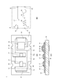
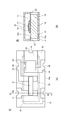
- FIG. 1A and 1B are diagrams showing a blocking element to which the present invention is applied, in which FIG. 1A is a plan view, FIG. 1B is a cross-sectional view taken along line A-A ′, and FIG. FIG. 2 is a circuit diagram of a blocking element to which the present invention is applied.
- FIG. 3 is a circuit diagram of a blocking element circuit to which the present invention is applied.
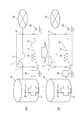
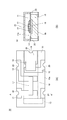
- 4A and 4B are diagrams showing a state in which the first soluble conductor of the breaking element to which the present invention is applied is blown, wherein FIG. 4A is a plan view, FIG. 4B is a circuit diagram, and FIG. 4C is a cross-sectional view. It is.
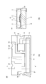
- FIG. 5A and 5B are diagrams showing a state where the second soluble conductor of the interrupting element to which the present invention is applied is melted, where FIG. 5A is a plan view, FIG. 5B is a circuit diagram, and FIG. 5C is a cross-sectional view.
- FIG. 6A and 6B are diagrams showing an application example of a blocking element to which the present invention is applied, in which FIG. 6A shows before the first and second fusible conductors are blown, and FIG. 6B shows after the fusing.
- 7A and 7B are diagrams showing another blocking element to which the present invention is applied, in which FIG. 7A is a plan view and FIG. 7B is a cross-sectional view taken along line A-A ′.
- FIG. 8A and 8B are diagrams showing another blocking element to which the present invention is applied, in which FIG. 8A is a plan view and FIG. 8B is a cross-sectional view taken along line A-A ′.
- 9A and 9B are diagrams showing another blocking element to which the present invention is applied, in which FIG. 9A is a plan view and FIG. 9B is a cross-sectional view taken along line A-A ′.
- 10A and 10B are diagrams showing another blocking element to which the present invention is applied, in which FIG. 10A is a plan view and FIG. 10B is a cross-sectional view along A-A ′.
- FIG. 10A is a plan view and FIG. 10B is a cross-sectional view along A-A ′.
- FIG. 11 is a perspective view showing a soluble conductor having a high melting point metal layer and a low melting point metal layer and having a covering structure
- FIG. 11A is a structure in which the high melting point metal layer is used as an inner layer and is covered with a low melting point metal layer.
- B shows a structure in which a low melting point metal layer is used as an inner layer and is covered with a high melting point metal layer.
- FIG. 12 is a perspective view showing a soluble conductor having a laminated structure of a high melting point metal layer and a low melting point metal layer, where (A) shows an upper and lower two layer structure, and (B) shows a three layer structure of an inner layer and an outer layer. .
- FIG. 13 is a cross-sectional view showing a soluble conductor having a multilayer structure of a high melting point metal layer and a low melting point metal layer.
- FIG. 14 is a plan view showing a fusible conductor in which a linear opening is formed on the surface of the refractory metal layer and the low melting metal layer is exposed, and (A) shows the opening along the longitudinal direction. The formed part (B) has an opening formed in the width direction.
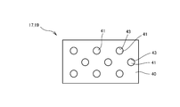
- FIG. 15 is a plan view showing a soluble conductor in which a circular opening is formed on the surface of the high melting point metal layer and the low melting point metal layer is exposed.
- FIG. 16 is a plan view showing a soluble conductor in which a circular opening is formed in a refractory metal layer and a low melting point metal is filled therein.
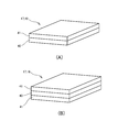
- FIG. 17 is a plan view showing a blocking element according to a reference example of the present invention.
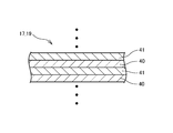
- FIG. 18 is a circuit diagram of a blocking element according to a reference example of the present invention.
- a blocking element 1 to which the present invention is applied includes an insulating substrate 10, a first electrode 11 and a second electrode 12 that are formed on the insulating substrate 10 and constitute a first circuit 2.
- the third electrode 13, the fourth electrode 14, and the fifth electrode 15, which are formed on the insulating substrate 10 and constitute the second circuit 3, are mounted across the first and second electrodes 11 and 12.
- a fusible conductor (fuse) 19 is provided.
- 1A is a plan view of the blocking element 1
- FIG. 1B is a cross-sectional view along AA ′
- FIG. 1C is a cross-sectional view.
- the insulating substrate 10 is formed of an insulating member such as alumina, glass ceramics, mullite, or zirconia.
- an insulating member such as alumina, glass ceramics, mullite, or zirconia.
- the material used for printed wiring boards such as a glass epoxy board
- the first and second electrodes 11 and 12 are formed on the surface 10a of the insulating substrate 10 and are stacked on an insulating member 21 described later. Further, the first and second electrodes 11 and 12 are connected to external connection terminals formed on the back surface 10 b of the insulating substrate 10 through the through holes 20.
- the first and second electrodes 11 and 12 are electrically connected by mounting the first soluble conductor 17.
- the blocking element 1 constitutes the first circuit 2 that extends from the first electrode 11 to the first soluble conductor 17 to the second electrode 12, and the first circuit 2 is mounted by the blocking element 1. Embedded in a part of a circuit formed on a circuit board to be processed.
- a circuit in which the first circuit 2 is incorporated is a current line of an electronic device in which the blocking element 1 is mounted.
- a charge / discharge circuit in a battery pack of a lithium ion secondary battery, a power supply circuit of various electronic devices, or a digital The present invention can be applied to any circuit such as a signal circuit that requires a physical current path to be cut off regardless of the strength of the current.
- the heating element 18 is laminated on the surface 10 a of the insulating substrate 10 and is covered with the insulating member 21.
- the heating element 18 is a conductive member that has a relatively high resistance value and generates heat when energized, and is made of, for example, W, Mo, Ru, or the like. It is formed by mixing powders of these alloys, compositions, or compounds with a resin binder or the like, forming a paste on the insulating substrate 10 using a screen printing technique, and firing the pattern. .
- the heating element 18 has one end connected to the third electrode 13 and the other end connected to the fourth electrode 14.
- An insulating member 21 is disposed so as to cover the heating element 18, and the first electrode 11, the second electrode 12, the fourth electrode 14, and the fifth electrode are overlapped with the heating element 18 through the insulating member 21.
- the electrode 15 is laminated.
- the insulating member 21 for example, glass can be used.
- the interrupting element 1 also laminates an insulating member between the heating element 18 and the insulating substrate 10, and the heating element 18 is connected to the insulating substrate. You may provide in the inside of the insulating member 21 formed in the surface of 10.
- the third electrode 13 is formed on the surface 10 a of the insulating substrate 10 and is connected to one end of the heating element 18.
- the fourth electrode 14 is connected to the other end of the heating element 18 by being formed on the surface 10 a of the insulating substrate 10, and is stacked on the insulating member 21.
- the fifth electrode 15 is formed on the surface 10 a of the insulating member 10 and is stacked on the insulating member 21.
- the third electrode 13 and the fifth electrode 15 are connected to the external connection terminal formed on the back surface 10 b of the insulating substrate 10 through the through hole 20.
- the fourth and fifth electrodes 14 and 15 are electrically connected by mounting the second soluble conductor 19 on the insulating member 21.
- the third to fifth electrodes 13 to 15 constitute a second circuit 3 that is electrically independent of the first circuit 2.
- the second circuit 3 is a circuit for heating and fusing the first fusible conductor 17 of the first circuit 2, and after fusing the first fusible conductor 17 and shutting off the first circuit 2. Cuts the second fusible conductor 19 and cuts off itself to stop the power supply to the heating element 18.
- the first and second fusible conductors 17 and 19 can use any metal that is quickly melted by the heat generated by the heating element 18, for example, a low melting point metal such as Pb-free solder containing Sn as a main component. Can be suitably used.
- the first and second soluble conductors 17 and 19 may contain a low melting point metal and a high melting point metal.
- the low melting point metal it is preferable to use solder such as Pb-free solder, and as the high melting point metal, it is preferable to use Ag, Cu or an alloy containing these as a main component.
- the high melting point metal and the low melting point metal even when the reflow temperature exceeds the melting temperature of the low melting point metal and the low melting point metal melts when the blocking element 1 is reflow mounted, the low melting point of the inner layer The outflow of the metal to the outside can be suppressed, and the shapes of the first and second soluble conductors 17 and 19 can be maintained.
- the first to third fusible conductors 21 to 23 can be formed by various configurations as will be described later.
- the first and second fusible conductors 17 and 19 can be configured with a low melting point metal layer as an inner layer and a high melting point metal layer as an outer layer.
- Such first and second fusible conductors 17 and 19 can be formed by forming a high melting point metal layer on a low melting point metal foil using a plating technique, or other well-known methods. It can also be formed using a lamination technique or a film formation technique.
- the first and second soluble conductors 17 and 19 may be configured such that the high melting point metal layer is an inner layer and the low melting point metal layer is an outer layer, and the low melting point metal layer and the high melting point metal layer are alternately arranged. It is good also as a multilayered structure of four or more layers laminated
- the first and second fusible conductors 17 and 19 are connected to the first and second electrodes 11 and 12 and the fourth and fifth electrodes 14 and 15 using solder or the like. .
- the first circuit 2 when the first circuit 2 is applied to a digital signal circuit, it is preferable to form a silver plating layer with good high frequency characteristics as the outer layer of the first soluble conductor 17.
- the first soluble conductor 17 reduces the resistance by the skin effect and improves the high frequency characteristics, and also flows through the outer silver-plated layer even when an instantaneous large current flows, so that fusing due to self-heating occurs. It is possible to improve the pulse resistance for preventing the above.
- the blocking element 1 is formed such that the first soluble conductor 17 of the first circuit 2 is blown before the second soluble conductor 19 of the second circuit 3. This is because if the second soluble conductor 19 is blown before the first soluble conductor 17, the power supply to the heating element 18 is stopped and the first soluble conductor 17 cannot be blown.
- the blocking element 1 is formed such that when the heating element 18 generates heat, the first soluble conductor 17 is blown first. Specifically, the first soluble conductor 17 of the blocking element 1 is mounted at a position closer to the heat generation center of the heating element 18 than the second soluble conductor 19.
- the heat generation center of the heating element 18 refers to a region where the temperature becomes the highest in the initial stage of heat generation in the heat distribution that is generated when the heating element 18 generates heat.
- the heat generated from the heating element 18 has the largest amount of heat dissipated from the insulating substrate 10, and when the insulating substrate 10 is formed of a ceramic material having excellent thermal shock resistance but high thermal conductivity, the insulating substrate 10 The heat will diffuse. For this reason, in the initial stage of heat generation when energization is started, the heating element 18 is most heated at the center farthest from the outer edge in contact with the insulating substrate 10 and is radiated toward the outer edge in contact with the insulating substrate 10, so that the temperature hardly rises.
- the blocking element 1 has the second fusible conductor 17 mounted on a position closer to the heat generating center that is the highest temperature in the initial stage of heat generation of the heat generating element 18 than the second fusible conductor 19. Heat is transmitted earlier than the fusible conductor 19 so that it melts. Since the second soluble conductor 19 is heated later than the first soluble conductor 17, the second soluble conductor 19 is blown after the first soluble conductor 17 is blown.
- blocking element 1 may make it the 1st soluble conductor 17 blow out previously by changing the shape of the 1st, 2nd soluble conductors 17 and 19.
- FIG. since the first and second fusible conductors 17 and 19 become easier to cut as the cross-sectional area is smaller, the breaking element 1 has the second fusible conductor 17 having a cross-sectional area equal to the second fusible conductor 17. By making it smaller than the cross-sectional area of the conductor 19, it can be blown before the second soluble conductor 19.
- blocking element 1 forms the 1st soluble conductor 17 narrowly and long along the electric current path between the 1st, 2nd electrodes 11 and 12, and makes the 2nd soluble conductor 19 4th. It may be formed wide and short along the current path between the fifth electrodes 14 and 15.
- the first soluble conductor 17 has a shape that is relatively easier to blow than the second soluble conductor 19, and is blown earlier than the second soluble conductor 19 due to the heat generated by the heating element 18. .
- the blocking element 1 may be formed of a material having a lower melting point than the material of the second soluble conductor 19 as the material of the first soluble conductor 17. This also makes the first soluble conductor 17 easier to blow than the second soluble conductor 19 due to the heat generated by the heating element 18, and ensures that the first soluble conductor 17 is more reliable than the second soluble conductor 19. Can be blown first.
- the blocking element 1 provides a difference in melting point by changing the layer structure of the first soluble conductor 17 and the second soluble conductor 19, and relatively replaces the first soluble conductor 17 with the second soluble conductor 17.
- the first soluble conductor 17 may be blown earlier than the second soluble conductor 19 by the heat generation of the heating element 18.
- the cover member 23 is formed by using an insulating member such as a thermoplastic plastic, a ceramic, a glass epoxy substrate, etc., like the insulating substrate 10.
- FIG. 2 shows a circuit diagram of the blocking element 1.
- FIG. 3 shows an example of a cutoff element circuit 30 to which the cutoff element 1 is applied.
- the blocking element 1 has a first circuit 2 formed by a first electrode 11 and a second electrode 12 being connected via a first soluble conductor 17.
- the first circuit 2 is incorporated in various external circuits 31 such as a power supply circuit and a digital signal circuit by being connected in series on the current path of the circuit board on which the blocking element 1 is mounted.
- the blocking element 1 has a second circuit 3 in which a heating element 18 and a second soluble conductor 19 are connected in series via a fourth electrode 14.
- the second circuit 3 is electrically independent of the first circuit 2 and can be thermally connected.
- the heating element 18 has one end connected to the third electrode 13 and the other end connected to the fourth electrode 14.
- the second soluble conductor 19 is mounted between the fourth electrode 14 and the fifth electrode 15.
- the third electrode 13 is connected to a current control element 25 that controls power supply to the second circuit 3 via an external connection terminal, and the fifth electrode 15 is connected to an external power supply 26 via an external connection terminal. Is done.
- the current control element 25 is a switch element that controls power feeding to the second circuit 3, and is configured by, for example, an FET, and a detection circuit that detects whether or not the first circuit 2 needs to be electrically and physically disconnected. 27.
- the detection circuit 27 is a circuit that detects a situation in which various circuits in which the first circuit 2 of the blocking element 1 is incorporated need to be cut off. For example, an abnormal voltage of a battery pack, hacking or cracking in a network communication device, or The current control element 25 is operated when it is necessary to cut off the current path physically and irreversibly due to the interruption of the first circuit 2 such as the expiration of the license period of the software, etc.
- the electric power of the external power supply 26 is supplied to the second circuit 3, and the first fusible conductor 17 is blown by the heat generating body 18 generating heat (FIGS. 4A, 4B, and 4C). .
- the molten conductor of the first soluble conductor 17 is attracted onto the first electrode 11 and the second electrode 12 having high wettability. Therefore, the 1st soluble conductor 17 can interrupt
- the second circuit 3 reliably supplies power to the heating element 18 until the first circuit 2 is cut off. Can generate heat.
- the heating element 18 continues to generate heat even after the first fusible conductor 17 is blown, but the second fusible conductor 19 is also blown after the first fusible conductor 17 to cut off the second circuit 3. (FIGS. 5A, 5B, and 5C). Thereby, the electric power feeding to the heat generating body 18 is also stopped.
- the first circuit 2 incorporated in the external circuit 31 and the second circuit 3 that blocks the first circuit are electrically independent. Therefore, regardless of the type of the external circuit 31, it is possible to supply electric power that obtains a sufficient amount of heat generation for fusing the first soluble conductor 17 to the heating element 18. Therefore, according to the interruption
- the blocking element 1 and the blocking element circuit 30 include the first circuit 2 between the data server 33 and the Internet line 34 for the purpose of information security.
- the signal line is physically and irreversibly disconnected from the Internet line 34 by blocking the first circuit 2 to prevent information leakage. be able to.
- the blocking element 1 and the blocking element circuit 30 can be applied to canceling the physical license authentication of the device and stopping the function with respect to the device remodeling action as a PL (Product Liability) countermeasure.
- the electric current control element which controls the electric power feeding to the heat generating body 18 25 can be selected according to the rating of the heating element 18 regardless of the rating of the first circuit 2, and can be manufactured at a lower cost.
- the blocking element is formed by forming a heating element 18 on the surface 10a of the insulating substrate 10 on which the first to fifth electrodes 11 to 15 are formed, and the first and second electrodes 11, 12 and the fourth and fifth electrodes 14 and 15 are overlapped, as shown in FIG. 7, opposite to the surface 10a of the insulating substrate 10 on which the first to fifth electrodes 11 to 15 are formed.
- FIG. 7A is a plan view of the blocking element 40 in which the heating element 18 is formed on the back surface of the insulating substrate 10, and
- FIG. 7B is a cross-sectional view along AA ′.
- symbol is attached
- one end of the third electrode 13 and the fourth electrode 14 is also formed on the back surface 10b side of the insulating substrate 10.
- the other end of the fourth electrode 14 is formed on the surface 10 a of the insulating substrate 10, and a second soluble conductor 19 is mounted between the fourth electrode 14 and the fifth electrode 15.
- One end and the other end of the fourth electrode 14 are continuous through the through hole 20.
- the heating element 18 is formed on the back surface 10b of the insulating substrate 10 so that the surface 10a of the insulating substrate 10 becomes flat, and other than the first and second electrodes 11 and 12 and the fourth electrode 14.
- the end side and the fifth electrode 15 can be formed by a simple process.
- the insulating member 21 is formed on the heating element 18 to protect the heating element 18 and to ensure insulation when the blocking element 1 is mounted.
- the heating element 18 and the first and second electrodes 11 and 12 are overlapped so that the first soluble conductor 17 is closer to the heating center of the heating element 18 than the second soluble conductor 19. It is preferable to arrange in. Further, the heating element 18 and the fourth and fifth electrodes 14 and 15 may be overlapped so that the heat of the heating element 18 can be efficiently transmitted to the second soluble conductor 19.
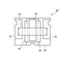
- blocking element may form the heat generating body 18 in the inside of the insulated substrate 10, as shown in FIG. 8A is a plan view of the blocking element 50 in which the heating element 18 is formed inside the insulating substrate 10, and FIG. 8B is a cross-sectional view along AA ′.
- symbol is attached
- the blocking element 50 is formed by forming one end of the heating element 18, the third electrode 13, and the fourth electrode 14 on the surface and then laminating a ceramic material.
- the insulating substrate 10 having the heating element 18 formed therein can be obtained.
- One end of each of the third electrode 13 and the fourth electrode 14 is connected to the other end formed on the front surface 10a or the back surface 10b of the insulating substrate 10 through the through hole 20, respectively.
- the surface 10 a of the insulating substrate 10 is flattened by forming the heating element 18 inside the insulating substrate 10, and the first and second electrodes 11, 12, and the fourth electrode 14 are provided.
- the end side and the fifth electrode 15 can be formed by a simple process.
- the heat generating body 18 is formed inside the insulating substrate 10 in the blocking element 50, it is not necessary to provide the insulating member 21.
- the heating element 18 and the first and second electrodes 11 and 12 are overlapped so that the first soluble conductor 17 is closer to the heating center of the heating element 18 than the second soluble conductor 19. It is preferable to arrange in. Further, the heating element 18 and the fourth and fifth electrodes 14 and 15 may be overlapped so that the heat of the heating element 18 can be efficiently transmitted to the second soluble conductor 19.
- the interrupting element 1 includes the heating element 18 on the surface 10 a of the insulating substrate 10, the first and second electrodes 11 and 12, and the fourth and fifth electrodes 14 and 15. May be formed side by side.
- FIG. 9A shows a blocking element 60 in which the heating element 18 is formed side by side with the first and second electrodes 11 and 12 and the fourth and fifth electrodes 14 and 15 on the surface of the insulating substrate 10.
- FIG. 9B is a plan view, and FIG. 9B is a cross-sectional view along AA ′.
- symbol is attached
- the first soluble conductor 17 is arranged closer to the heat generating center of the heating element 18 than the second soluble conductor 19. Further, as shown in FIGS. 10A and 10B, only the first and second electrodes 11 and 12 are superimposed on the heating element 18 via the insulating member 21, and only the first soluble conductor 17 is provided. You may superimpose on the heat generating body 18. Thereby, the 1st soluble conductor 17 is arrange
- any or all of the first and second soluble conductors 17 and 19 may contain a low melting point metal and a high melting point metal.
- the first and second soluble conductors 17 and 19 are provided with a refractory metal layer 40 made of Ag, Cu or an alloy containing these as a main component as an inner layer.
- a soluble conductor provided with a low melting point metal layer 41 made of Pb-free solder containing Sn as a main component as an outer layer may be used.
- the first and second fusible conductors 17 and 19 may have a structure in which the entire surface of the high melting point metal layer 40 is covered with the low melting point metal layer 41, and is covered except for a pair of opposing side surfaces. It may be a structure.
- the covering structure with the high melting point metal layer 40 and the low melting point metal layer 41 can be formed using a known film forming technique such as plating.
- the first and second soluble conductors 17 and 19 are soluble in which a low melting point metal layer 41 is provided as an inner layer and a high melting point metal layer 40 is provided as an outer layer.
- a conductor may be used.
- the first and second fusible conductors 17 and 19 may have a structure in which the entire surface of the low melting point metal layer 41 is covered with the high melting point metal layer 40 and is covered except for a pair of opposing side surfaces. The structure may be different.
- the first and second soluble conductors 17 and 19 may have a laminated structure in which a refractory metal layer 40 and a low-melting metal layer 41 are laminated as shown in FIG.
- the first and second soluble conductors 17 and 19 are mounted on the first and second electrodes 11 and 12 and the fourth and fifth electrodes 14 and 15 as shown in FIG.
- the lower melting point metal layer 41 may be stacked on the upper surface of the lower refractory metal layer 40, and the lower layer may be stacked on the upper surface of the lower melting point metal layer 40.
- the upper refractory metal layer 40 may be laminated on the upper surface of the lower melting point metal layer 41.
- the first and second soluble conductors 17 and 19 may be formed as a three-layer structure including an inner layer and an outer layer laminated on the upper and lower surfaces of the inner layer, as shown in FIG.
- the low melting point metal layer 41 serving as the outer layer may be laminated on the upper and lower surfaces of the refractory metal layer 40 serving as the inner layer, and the refractory metal layer 40 serving as the outer layer may be disposed on the upper and lower surfaces of the low melting point metal layer 41 serving as the inner layer. You may laminate.
- the 1st, 2nd soluble conductors 17 and 19 are good also as a multilayered structure of 4 or more layers by which the high melting metal layer 40 and the low melting metal layer 41 were laminated
- the 1st, 2nd soluble conductors 17 and 19 are good also as a structure coat
- the high melting point metal layer 40 may be partially laminated in a stripe shape on the surface of the low melting point metal layer 41 constituting the inner layer.
- FIG. 14 is a plan view of the first and second fusible conductors 17 and 19.
- the first and second fusible conductors 17 and 19 shown in FIG. 14A have a plurality of linear refractory metal layers 40 in the longitudinal direction on the surface of the low melting point metal layer 41 at predetermined intervals in the width direction.
- a linear opening 42 is formed along the longitudinal direction, and the low melting point metal layer 41 is exposed from the opening 42.
- the low melting point metal layer 41 is exposed from the opening 42, thereby increasing the contact area between the molten low melting point metal and the high melting point metal, and the high melting point metal layer 40. It is possible to improve the fusing property by further promoting the erosion action.
- the opening 42 can be formed, for example, by subjecting the low melting point metal layer 41 to partial plating of a metal constituting the high melting point metal layer 40.
- the first and second soluble conductors 17 and 19 are formed on the surface of the low melting point metal layer 41 at a predetermined interval in the longitudinal direction at the linear refractory metal layer 40.
- the linear openings 42 may be formed along the width direction.
- the first and second fusible conductors 17 and 19 form the refractory metal layer 40 on the surface of the low melting point metal layer 41 and extend over the entire surface of the refractory metal layer 40.
- a circular opening 43 may be formed, and the low melting point metal layer 41 may be exposed from the opening 43.
- the opening 43 can be formed, for example, by subjecting the low melting point metal layer 41 to partial plating of a metal constituting the high melting point metal layer 40.
- the low melting point metal layer 41 is exposed from the opening 43, thereby increasing the contact area between the molten low melting point metal and the high melting point metal, and erosion of the high melting point metal.
- the action can be further promoted to improve the fusing property.
- the first and second fusible conductors 17 and 19 are formed with a large number of openings 44 in the refractory metal layer 40 as an inner layer, and the refractory metal layer 40 is plated.
- the low melting point metal layer 41 may be formed using a technique or the like and filled in the opening 44.
- the first and second fusible conductors 17 and 19 have an increased area where the molten low melting point metal contacts the high melting point metal, so that the low melting point metal erodes the high melting point metal in a shorter time. Will be able to.
- the first and second soluble conductors 17 and 19 are preferably formed such that the volume of the low melting point metal layer 41 is larger than the volume of the high melting point metal layer 40.
- the first and second soluble conductors 17 and 19 are heated by the heating element 18, the low melting point metal melts to cause the high melting point metal to be eroded, thereby quickly melting and fusing. . Therefore, the first and second soluble conductors 17 and 19 promote the erosion action by forming the volume of the low melting point metal layer 41 larger than the volume of the high melting point metal layer 40, and promptly. Blocking between the first and second electrodes 11 and 12 and blocking between the fourth and fifth electrodes 14 and 15 can be performed.
Landscapes
- Chemical & Material Sciences (AREA)
- Engineering & Computer Science (AREA)
- Combustion & Propulsion (AREA)
- Chemical Kinetics & Catalysis (AREA)
- Electrochemistry (AREA)
- General Chemical & Material Sciences (AREA)
- Fuses (AREA)
- Emergency Protection Circuit Devices (AREA)
Priority Applications (2)
| Application Number | Priority Date | Filing Date | Title |
|---|---|---|---|
| KR1020157035050A KR102275927B1 (ko) | 2013-08-28 | 2014-08-27 | 차단 소자 및 차단 소자 회로 |
| CN201480047053.7A CN105493219A (zh) | 2013-08-28 | 2014-08-27 | 切断元件和切断元件电路 |
Applications Claiming Priority (2)
| Application Number | Priority Date | Filing Date | Title |
|---|---|---|---|
| JP2013-177058 | 2013-08-28 | ||
| JP2013177058A JP6184805B2 (ja) | 2013-08-28 | 2013-08-28 | 遮断素子、及び遮断素子回路 |
Publications (1)
| Publication Number | Publication Date |
|---|---|
| WO2015030020A1 true WO2015030020A1 (ja) | 2015-03-05 |
Family
ID=52586572
Family Applications (1)
| Application Number | Title | Priority Date | Filing Date |
|---|---|---|---|
| PCT/JP2014/072348 Ceased WO2015030020A1 (ja) | 2013-08-28 | 2014-08-27 | 遮断素子、及び遮断素子回路 |
Country Status (5)
| Country | Link |
|---|---|
| JP (1) | JP6184805B2 (enExample) |
| KR (1) | KR102275927B1 (enExample) |
| CN (2) | CN110957188A (enExample) |
| TW (1) | TWI629702B (enExample) |
| WO (1) | WO2015030020A1 (enExample) |
Families Citing this family (4)
| Publication number | Priority date | Publication date | Assignee | Title |
|---|---|---|---|---|
| JP6483524B2 (ja) * | 2015-05-22 | 2019-03-13 | デクセリアルズ株式会社 | 保護素子、二次電池の保護回路、電池パックおよび電池状態管理システム |
| JP7154090B2 (ja) * | 2018-10-01 | 2022-10-17 | ショット日本株式会社 | 保護素子 |
| US12293889B2 (en) | 2020-05-29 | 2025-05-06 | Dexerials Corporation | Protective circuit |
| JP2024049240A (ja) * | 2022-09-28 | 2024-04-09 | デクセリアルズ株式会社 | 保護素子及び保護素子の製造方法 |
Citations (3)
| Publication number | Priority date | Publication date | Assignee | Title |
|---|---|---|---|---|
| JP2001035331A (ja) * | 1999-07-19 | 2001-02-09 | Sony Corp | スイッチング素子 |
| JP2004185960A (ja) * | 2002-12-03 | 2004-07-02 | Kamaya Denki Kk | 回路保護素子とその製造方法 |
| JP2007135359A (ja) * | 2005-11-11 | 2007-05-31 | Sanyo Electric Co Ltd | 保護素子とこの保護素子を備えるパック電池 |
Family Cites Families (11)
| Publication number | Priority date | Publication date | Assignee | Title |
|---|---|---|---|---|
| JP3774871B2 (ja) * | 1995-10-16 | 2006-05-17 | 松尾電機株式会社 | 遅延型薄膜ヒューズ |
| JPH1056742A (ja) * | 1996-08-06 | 1998-02-24 | Matsushita Electric Ind Co Ltd | 二次電池の過充電保護回路 |
| JP2000200529A (ja) * | 1999-01-07 | 2000-07-18 | Nec Kansai Ltd | 保護素子およびその製造方法 |
| JP4464554B2 (ja) * | 2000-12-14 | 2010-05-19 | 北陸電気工業株式会社 | ヒューズ素子及びチップ型ヒューズ |
| EP1300867A1 (fr) * | 2001-10-03 | 2003-04-09 | Metalor Technologies International S.A. | Element de fusible et son procédé de fabrication |
| JP4624489B2 (ja) * | 2005-08-05 | 2011-02-02 | 内橋エステック株式会社 | ケースタイプ合金型温度ヒューズの製作方法及びケースタイプ合金型温度ヒューズ |
| US20070075822A1 (en) * | 2005-10-03 | 2007-04-05 | Littlefuse, Inc. | Fuse with cavity forming enclosure |
| JP5072796B2 (ja) | 2008-05-23 | 2012-11-14 | ソニーケミカル&インフォメーションデバイス株式会社 | 保護素子及び二次電池装置 |
| JP5301298B2 (ja) * | 2009-01-21 | 2013-09-25 | デクセリアルズ株式会社 | 保護素子 |
| JP5656466B2 (ja) | 2010-06-15 | 2015-01-21 | デクセリアルズ株式会社 | 保護素子、及び、保護素子の製造方法 |
| CN102290301B (zh) * | 2010-06-18 | 2014-04-02 | 厦门赛尔特电子有限公司 | 一种大电流熔断器 |
-
2013
- 2013-08-28 JP JP2013177058A patent/JP6184805B2/ja active Active
-
2014
- 2014-08-27 CN CN201911368547.6A patent/CN110957188A/zh active Pending
- 2014-08-27 WO PCT/JP2014/072348 patent/WO2015030020A1/ja not_active Ceased
- 2014-08-27 KR KR1020157035050A patent/KR102275927B1/ko active Active
- 2014-08-27 CN CN201480047053.7A patent/CN105493219A/zh active Pending
- 2014-08-27 TW TW103129444A patent/TWI629702B/zh active
Patent Citations (3)
| Publication number | Priority date | Publication date | Assignee | Title |
|---|---|---|---|---|
| JP2001035331A (ja) * | 1999-07-19 | 2001-02-09 | Sony Corp | スイッチング素子 |
| JP2004185960A (ja) * | 2002-12-03 | 2004-07-02 | Kamaya Denki Kk | 回路保護素子とその製造方法 |
| JP2007135359A (ja) * | 2005-11-11 | 2007-05-31 | Sanyo Electric Co Ltd | 保護素子とこの保護素子を備えるパック電池 |
Also Published As
| Publication number | Publication date |
|---|---|
| KR20160046762A (ko) | 2016-04-29 |
| TWI629702B (zh) | 2018-07-11 |
| KR102275927B1 (ko) | 2021-07-12 |
| TW201523680A (zh) | 2015-06-16 |
| JP6184805B2 (ja) | 2017-08-23 |
| JP2015046316A (ja) | 2015-03-12 |
| CN105493219A (zh) | 2016-04-13 |
| CN110957188A (zh) | 2020-04-03 |
Similar Documents
| Publication | Publication Date | Title |
|---|---|---|
| JP6249602B2 (ja) | 保護素子 | |
| KR102523229B1 (ko) | 보호 소자 및 실장체 | |
| JP6621255B2 (ja) | 保護素子、ヒューズ素子 | |
| JP2015035281A (ja) | 保護素子、及びこれを用いた保護回路基板 | |
| JP6381980B2 (ja) | スイッチ素子及びスイッチ回路 | |
| JP6173859B2 (ja) | 短絡素子 | |
| KR102386943B1 (ko) | 단락 소자 | |
| JP6184805B2 (ja) | 遮断素子、及び遮断素子回路 | |
| KR102263795B1 (ko) | 차단 소자 및 차단 소자 회로 | |
| KR102233539B1 (ko) | 단락 소자 및 단락 회로 | |
| JP2018018835A (ja) | 保護素子、ヒューズ素子 | |
| JP6202992B2 (ja) | 保護回路、バッテリ回路、保護素子、保護素子の駆動方法 | |
| TWI685870B (zh) | 短路元件 | |
| TWI615940B (zh) | 短路元件 |
Legal Events
| Date | Code | Title | Description |
|---|---|---|---|
| WWE | Wipo information: entry into national phase |
Ref document number: 201480047053.7 Country of ref document: CN |
|
| 121 | Ep: the epo has been informed by wipo that ep was designated in this application |
Ref document number: 14840629 Country of ref document: EP Kind code of ref document: A1 |
|
| ENP | Entry into the national phase |
Ref document number: 20157035050 Country of ref document: KR Kind code of ref document: A |
|
| NENP | Non-entry into the national phase |
Ref country code: DE |
|
| 122 | Ep: pct application non-entry in european phase |
Ref document number: 14840629 Country of ref document: EP Kind code of ref document: A1 |