WO2015029211A1 - 光半導体装置用リードフレーム用の基体とその製造方法、これを用いた光半導体装置用リードフレームとその製造方法、および光半導体装置 - Google Patents
光半導体装置用リードフレーム用の基体とその製造方法、これを用いた光半導体装置用リードフレームとその製造方法、および光半導体装置 Download PDFInfo
- Publication number
- WO2015029211A1 WO2015029211A1 PCT/JP2013/073298 JP2013073298W WO2015029211A1 WO 2015029211 A1 WO2015029211 A1 WO 2015029211A1 JP 2013073298 W JP2013073298 W JP 2013073298W WO 2015029211 A1 WO2015029211 A1 WO 2015029211A1
- Authority
- WO
- WIPO (PCT)
- Prior art keywords
- optical semiconductor
- semiconductor device
- lead frame
- rolling
- substrate
- Prior art date
- Legal status (The legal status is an assumption and is not a legal conclusion. Google has not performed a legal analysis and makes no representation as to the accuracy of the status listed.)
- Ceased
Links
Images



Classifications
-
- H—ELECTRICITY
- H10—SEMICONDUCTOR DEVICES; ELECTRIC SOLID-STATE DEVICES NOT OTHERWISE PROVIDED FOR
- H10H—INORGANIC LIGHT-EMITTING SEMICONDUCTOR DEVICES HAVING POTENTIAL BARRIERS
- H10H20/00—Individual inorganic light-emitting semiconductor devices having potential barriers, e.g. light-emitting diodes [LED]
- H10H20/80—Constructional details
- H10H20/85—Packages
- H10H20/857—Interconnections, e.g. lead-frames, bond wires or solder balls
-
- H—ELECTRICITY
- H10—SEMICONDUCTOR DEVICES; ELECTRIC SOLID-STATE DEVICES NOT OTHERWISE PROVIDED FOR
- H10H—INORGANIC LIGHT-EMITTING SEMICONDUCTOR DEVICES HAVING POTENTIAL BARRIERS
- H10H20/00—Individual inorganic light-emitting semiconductor devices having potential barriers, e.g. light-emitting diodes [LED]
- H10H20/01—Manufacture or treatment
- H10H20/036—Manufacture or treatment of packages
- H10H20/0364—Manufacture or treatment of packages of interconnections
-
- H—ELECTRICITY
- H10—SEMICONDUCTOR DEVICES; ELECTRIC SOLID-STATE DEVICES NOT OTHERWISE PROVIDED FOR
- H10H—INORGANIC LIGHT-EMITTING SEMICONDUCTOR DEVICES HAVING POTENTIAL BARRIERS
- H10H20/00—Individual inorganic light-emitting semiconductor devices having potential barriers, e.g. light-emitting diodes [LED]
- H10H20/80—Constructional details
- H10H20/81—Bodies
- H10H20/814—Bodies having reflecting means, e.g. semiconductor Bragg reflectors
Definitions
- the present invention relates to a base for a lead frame for an optical semiconductor device and a method for manufacturing the same, a lead frame for an optical semiconductor device using the same, a method for manufacturing the same, and an optical semiconductor device.
- Lead frames for optical semiconductor devices are widely used as constituent members of various display / illumination light sources that use light emitting elements, which are optical semiconductor elements such as LED (Light Emitting Diode) elements, as light sources.
- a lead frame is arranged on a substrate, and after the light emitting element is mounted on the lead frame, the deterioration of the light emitting element and its peripheral parts due to external factors such as heat, moisture, and oxidation are prevented.
- the light emitting element and its periphery are sealed with resin.
- the reflective material of the lead frame has a high reflectance in the entire visible light wavelength range (400 to 800 nm) (for example, the reflectance with respect to a reference material such as barium sulfate or aluminum oxide). 80% or more).
- a method of LED for forming white light a method of arranging three chips emitting all colors of red (R), green (G), and blue (B), and a yellow phosphor dispersed in a blue LED chip.
- a method using the sealing resin There are mainly three main methods: a method using the sealing resin, and a method using a sealing resin in which RGB phosphors are dispersed in LED chips in the near ultraviolet region.
- the reflective material of the optical semiconductor device is required to have a high reflectance in the near ultraviolet region (wavelength 340 to 400 nm) and the visible light region (wavelength 400 to 800 nm).
- a smooth substrate as the lead frame substrate.
- a base made of a copper alloy plate or strip is subjected to a rolling process after electrolytic treatment so that the glossiness at 20 ° incidence is 200% or more and the surface roughness Rz is 1.0 ⁇ m.
- the following smooth substrates have been proposed.
- Patent Document 1 describes that the glossiness is 200% or more and the surface roughness Rz is 1.0 ⁇ m or less, but there is no description regarding the measurement direction. This is because a processing trace called a rolling streak is generated in the rolling parallel direction on the surface of the substrate by the rolling process, but the glossiness may be greatly different depending on the measurement direction in the rolling parallel direction and the rolling perpendicular direction. In particular, as a lead frame substrate used in an optical semiconductor device, the rolling streaks appear uneven with respect to the reflection of light, and therefore the glossiness is high in both the rolling parallel (longitudinal) direction and the rolling perpendicular (width) direction. Is required.
- Patent Document 1 does not discuss these, and further studies are required as a lead frame base for an optical semiconductor device. Further, in recent years, there are cases where a lead frame is subjected to an overhang process to form a recess, and the side surface thereof is subjected to silver plating to form a high output type optical semiconductor device. At this time, unevenness due to the rolling streaks originated and cracks sometimes occurred during the overhanging process. For this reason, there is a need for a lead frame substrate for an optical semiconductor device having good overhanging workability, but no examination from this point of view is made in Patent Document 1.
- a layer (film) made of silver or a silver alloy is formed on the lead frame on which the LED element is mounted, in particular for the purpose of improving the light reflectance in the visible light region (hereinafter referred to as reflectance).
- the silver film has a high reflectance in the visible light region.
- a silver plating layer is formed on the reflection surface (Patent Document 2), or 200 or after the silver or silver alloy film is formed.
- heat treatment is performed at a temperature of 30 ° C. or more for 30 seconds or more, the crystal grain size of the film is in the range of 0.5 ⁇ m to 30 ⁇ m, and the surface roughness of the base material is 0.5 ⁇ m or more (Patent Document 3). It has been.
- the surface roughness Ra of the silver alloy reflective film is 2.0 nm or less (Patent Document 4).
- the reflectance is as low as about 10% when an LED chip with an emission wavelength of 375 nm is used as compared with, for example, a blue LED chip with an emission wavelength of 450 nm. Further, when the crystal grain size is adjusted by heat treatment, silver may be oxidized due to the influence of residual oxygen, and the reflectivity may be lowered, and a sufficient effect for improving the reflectivity may not be obtained.
- PVD physical vapor deposition
- sputtering and vapor deposition are used as the achievement method.
- the roughness is 2 nm or less, there is another problem that the adhesion to the mold resin formed in the optical semiconductor device is extremely poor.
- the present invention provides an optical semiconductor device lead frame used in an LED, photocoupler, photointerrupter, etc., and an optical semiconductor device lead frame substrate that is less prone to cracking even if it is stretched, and a method for manufacturing the same. It is another object of the present invention to provide a lead frame for an optical semiconductor device having a very good reflectivity in the near ultraviolet region to visible light region (wavelength 340 to 800 nm) using the substrate, and a method for manufacturing the same.
- the inventors measured the glossiness measured at an incident angle of 60 ° on the surface of the substrate of the lead frame for optical semiconductor devices formed by rolling. Overhanging process when the parallel and perpendicular directions are 500% or more and the ratio of the glossiness in the parallel direction to the glossiness in the perpendicular direction is within 0.8 to 1.2
- the present inventors have found that cracks do not easily occur even when the step is performed, and a lead frame substrate having excellent reflectance of light having a wavelength of 340 to 800 nm can be obtained.
- the lead frame for optical semiconductor devices with a high reflectance could be provided simply by performing silver or silver alloy plating using the base
- the concave portion for mounting the optical semiconductor element is formed on the lead frame to have a hooked shape.
- the base for lead frames for optical semiconductor devices as described.
- a method for producing a lead frame substrate for a semiconductor device wherein a rolling oil having a kinematic viscosity of 7 mm 2 / s or less is used and finish rolling is performed with a rolling tension of 200 to 600 MPa.
- An optical semiconductor element is mounted after forming a light reflection layer on the optical semiconductor element mounting portion using the lead frame substrate for an optical semiconductor device according to any one of (1) to (3).
- An optical semiconductor device characterized by comprising: (11) An optical semiconductor device comprising an optical semiconductor element mounted on the lead frame for an optical semiconductor device according to any one of (4) to (7).
- the present invention by adjusting the glossiness of the substrate surface to a predetermined relationship between the rolling parallel direction and the rolling perpendicular direction, even if the thickness of the reflective layer made of silver or a silver alloy provided on the substrate is reduced, The effect of rolling stripes generated on the surface of the substrate is remarkably reduced to obtain a substrate for an optical semiconductor device lead frame having light reflection characteristics having a remarkably high reflectance in the near ultraviolet region to the visible light region (wavelength 340 to 800 nm). be able to.
- the recess is formed by, for example, overhanging, the unevenness difference in the direction perpendicular to the rolling direction is small.
- the lead frame substrate for an optical semiconductor device of the present invention the silver or silver alloy provided on the surface of the lead frame on the substrate is adjusted by adjusting the glossiness of the substrate surface to a predetermined relationship between the rolling parallel direction and the rolling perpendicular direction. Even if the thickness of the reflective layer is reduced, the influence of rolling stripes generated on the surface of the substrate is remarkably reduced, and the light reflection characteristics having a remarkably high reflectance in the near ultraviolet region to the visible light region (wavelength 340 to 800 nm) A lead frame for an optical semiconductor device having the following can be obtained.
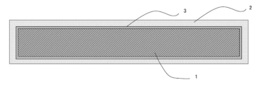
- FIG. 1 is an external view of a lead frame substrate for an optical semiconductor device according to the present invention.
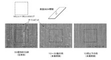
- FIG. 2 is an example of an SEM observation image with an observation magnification of 500 times on the surface of the lead frame substrate for optical semiconductor devices according to the present invention.
- FIG. 3 is a schematic cross-sectional view of an example of a lead frame for an optical semiconductor device using the lead frame substrate for an optical semiconductor device according to the present invention.
- FIG. 4 is a schematic cross-sectional view of another example of a lead frame for an optical semiconductor device using the lead frame substrate for an optical semiconductor device according to the present invention.
- FIG. 5 is a schematic cross-sectional view of still another example of a lead frame for an optical semiconductor device using the lead frame base for an optical semiconductor device according to the present invention.
- the glossiness measured at an incident angle of 60 ° on the surface of the optical semiconductor device lead frame substrate (1) formed by rolling is parallel to the rolling direction as shown in FIG.
- the ratio of the glossiness in the parallel direction to the glossiness in the perpendicular direction is 0.8 to 1.2, and the ratio is 0.8 to 1.2. It is preferably 0.9 to 1.1.
- the glossiness is, as defined in JIS Z 8741 (ISO 2813), a specular reflectance of 10% when a visible light is incident at an incident angle of 60 °, and a refractive index of 1.567.
- the actual glossiness is an average value of three measurements.
- the ratio between the glossiness in the parallel direction and the glossiness in the perpendicular direction within this range, the difference between the glossiness in the parallel direction and the glossiness in the perpendicular direction is reduced for the reflective layer of the lead frame provided on the substrate.
- the reflectance of the optical semiconductor device obtained thereby can be significantly increased from the near ultraviolet region to the visible light region.
- the number of oil pits formed on the surface of the substrate is 50 or less in an area of 100 ⁇ m ⁇ 100 ⁇ m.
- the oil pit here refers to a local recess that appears on the surface of the base plate or strip material by the lubricating oil taken in between the rolling roll and the material during cold rolling. Occurrence of the recesses includes conditions such as the diameter and roughness of the rolling roll, processing rate during rolling, processing conditions such as rolling speed, conditions such as temperature and viscosity of lubricating oil, mechanical strength of the plate or strip, crystal It can be changed depending on conditions such as the size of the grains. FIG.
- FIG. 2 is an SEM photograph obtained by photographing the surface of the substrate according to the present invention at an observation magnification of 500 times.
- the recess formed as shown in this figure is an oil pit. This number is preferably 50 or less in an area of 100 ⁇ m ⁇ 100 ⁇ m.
- the left photograph is a photograph of an example of a conventional substrate having an area of 100 ⁇ m ⁇ 100 ⁇ m and having more than 50 oil pits
- the center is a photograph of an example of the substrate of the present invention having 10-30 pieces
- the surface property of the substrate in the present invention greatly affects the adhesion between the mold resin formed in the optical semiconductor device and the substrate, and acts as follows.
- the surface texture is in a form having local recesses (oil pits).
- a material is formed by plating with a base layer and further a light reflecting layer with a thickness of 3 ⁇ m or less by a conventional method, even if either or both of them are gloss plating, the shape of the oil pit is changed. Reflected irregularities are formed.
- the anchor effect produced by the formed oil pit-like irregularities can improve the adhesion with the sealing resin when forming the optical semiconductor device.
- the degree of oil pit formation can be evaluated by counting the number of oil pits by, for example, SEM observation at an observation magnification of 500 times.
- the number of oil pits having a width of 5 ⁇ m or more and a depth of 10 ⁇ m or less is preferably 50 or less in 10,000 ⁇ m 2 , and this number is 15 or less. Is more preferable.
- FIG. 3 is an example of a schematic cross-sectional view thereof.
- the thickness of the reflective layer is more preferably 2 ⁇ m or less, and particularly preferably 1 ⁇ m or less.
- the thicker the reflective layer the better the light reflection characteristics obtained.
- the thickness of the reflective layer can be reduced, Excellent light reflection characteristics can be achieved.
- the minimum thickness exhibiting excellent reflectance is usually 0.1 ⁇ m or more, preferably 0.2 ⁇ m or more.
- a plating method As a method for forming the reflective layer, a plating method, a sputtering method, a vapor deposition method, and the like are possible. However, in consideration of productivity, a plating method, particularly a wet plating method is preferable, and an electrolytic plating method is more preferable.
- the surface roughness Sa is 3 nm or more and 50 nm or less as measured by an atomic force microscope on the surface of the reflective layer. Preferably, it is 3 nm or more and 10 nm or less.
- the surface roughness of the surface having a reflective layer in the present invention refers to the surface roughness obtained in the observation field of view with an atomic force microscope (AFM).
- AFM atomic force microscope
- the present inventors have found that the surface roughness is such that the frequency of dendritic precipitation after plating appears as this numerical value, and irregularities of the order of several tens of nanometers on the surface cause the reflectance to be reduced.
- a high sealing resin has excellent reflectivity with respect to light in both the near ultraviolet region having a wavelength of 340 to 400 nm and the visible light region in the vicinity of 400 nm to 800 nm.
- a lead frame for a semiconductor device having adhesiveness can be obtained.
- the surface roughness Sa having the reflective layer is preferably 50 nm or less, more preferably 30 nm or less, particularly preferably 10 nm or less, and most preferably 5 nm or less, whereby the reflectance of the LED component material is improved.
- the preferred reflectance in the present invention is, for example, when the reflective layer is formed of silver, the total reflectance is 90% or more in the visible light region (for example, 400 to 800 nm), particularly 90% or more at a wavelength of 450 nm. Yes, it is 95% or more at a wavelength of 600 nm.
- the reflectance is 95% or more at a wavelength of 450 nm, and this reflectivity has an effect of outputting excellent luminance as a lead frame for an optical semiconductor device equipped with a blue-emitting optical semiconductor element, and has a physical upper limit value. Infinitely close reflectance can be achieved. In addition, it indicates 80% or more at a wavelength of 375 nm in the near ultraviolet light region. In addition, when the surface roughness Sa is smaller than 2 nm, the adhesion with the sealing resin or the mold resin is extremely reduced. Therefore, the micro surface roughness is preferably 3 nm or more.
- a plating bath used in the electrolytic method for example, as a reflective layer is a conventional pure silver (Ag) bath, silver-selenium (Se). ) Bath, silver-antimony (Sb) bath, silver-selenium-antimony bath, silver-indium (In) bath, silver-gold (Au) bath, silver-platinum (Pt) bath, silver-tin (Sn) bath, etc.
- a coating thickness of 3 ⁇ m or less, more preferably 1.5 ⁇ m or less, can provide a lead frame for an optical semiconductor device with excellent reflectivity.
- the unevenness of the substrate cannot be sufficiently smoothed unless the coating thickness is 5 to 10 ⁇ m in order to improve smoothness, and the glossiness
- the reflectance cannot be increased because of a decrease in height.
- the substrate of the present invention it is possible to sufficiently increase the smoothness even with a thinner coating thickness.
- the coating thickness reduction effect is excellent in productivity, contributing to cost reduction, and a resource saving viewpoint. Therefore, it is possible to provide a lead frame for an optical semiconductor device that is environmentally friendly and extremely excellent in reflectance.
- the production process of the substrate is not particularly limited and can be obtained by a conventional method, but it is preferable to perform rolling at the end of the process.
- the desired thickness is obtained by rolling to provide mechanical strength and surface gloss smoothness.
- a total rolling reduction of 10% or more is usually added.
- a smooth rolling roll is used, and it is efficiently processed using a low-viscosity lubricating oil. If a higher gloss smoothness is required as required, polishing rolling is also performed without using a lubricant. Note that heat treatment may be performed during or after rolling as necessary.
- a metal base component Copper or a copper base alloy or iron or an iron base alloy is used.
- a copper alloy CDA (Copper Development Association) listed alloys “C14410 (Cu-0.15Sn, Furukawa Electric Co., Ltd., product name: EFTEC-3)”, “C19400 (Cu-Fe series) Alloy material, Cu-2.3Fe-0.03P-0.15Zn) "," C26000 (brass, Cu-30Zn) ",” C52100 (phosphor bronze, Cu-8Sn-0.15P) ",” C77000 (Western) White, Cu-18Ni-27Zn) ",” C18045 (Cu-0.3Cr-0.25Sn-0.5Zn, manufactured by Furukawa Electric Co., Ltd., product name: EFTEC-64T) "and the like can be used.
- the unit of the number before each element is mass%. Since these substrates have different electrical conductivity and strength, they are selected and used according to the required characteristics as appropriate. However, from the viewpoint of improving the heat dissipation of the lead frame for optical semiconductor devices, the electrical conductivity is copper with 60% IACS or more. It is preferable to use an alloy strip. Further, as the iron or iron-based alloy, for example, 42 alloy (Fe-42 mass% Ni) or the like is used.
- the thickness of the substrate is not particularly limited, but is usually 0.05 mm to 1 mm, preferably 0.1 mm to 0.8 mm.
- the condition of the rolling roll such as the roll roughness at the time of final rolling applied last, the type of rolling oil, and by changing the tensile strength at the time of rolling,
- the roughness of the substrate surface can be adjusted.
- the surface roughness of the roll at the time of finish rolling to be applied last is 0.05 ⁇ m or less in terms of arithmetic average roughness Ra.
- the tension during rolling is preferably 200 to 600 MPa.
- the lead frame for an optical semiconductor device of the present invention includes nickel, nickel alloy, cobalt, cobalt alloy, palladium, palladium alloy, rhodium, and rhodium alloy between the base and the reflective layer made of silver or a silver alloy.
- An intermediate layer made of a metal or alloy selected from the group may be provided.
- the intermediate layer is suitably formed by plating, for example.
- FIG. 4 shows an example of a schematic cross-sectional view in which the intermediate layer 3 is formed.
- the thermal conductivity of the material is relatively low, so by providing an intermediate layer made of copper or copper alloy as the intermediate layer, heat dissipation can be improved without impairing the reflectivity. Can do. Furthermore, since the intermediate layer which is the copper or copper alloy layer also contributes to the improvement of the plating adhesion between the reflective layer thereon and the underlying substrate, the adhesion due to heat generated when the light emitting element emits light. Deterioration can be prevented. In the case of using a copper or copper alloy substrate, an intermediate layer of nickel, nickel alloy, cobalt, or cobalt alloy is used as an intermediate layer in order to suppress diffusion of the substrate component to the reflective layer due to heat generated when the light emitting element emits light.
- the thickness of these intermediate layers is not particularly limited in the present invention, but is preferably in the range of 0.001 to 0.5 ⁇ m. Since the thickness of the intermediate layer is preferably the minimum necessary so as not to reduce the effect of improving the glossiness of the substrate, the range of 0.005 to 0.1 ⁇ m is particularly preferable.
- the reflective layer or the underlying intermediate layer is formed only at a necessary location, so that a coating material is used more than necessary. Therefore, an optical semiconductor device lead frame can be formed, and an environmentally friendly lead frame can be provided.
- FIG. 5 shows an example of a schematic cross-sectional view in which the reflective layer 2 is formed after the recess 4 is formed on the lead frame substrate 1 by overhanging.
- some high-powered products have a lead frame that is formed by mounting the optical semiconductor element on the bottom of the recess, but there is a case where cracking occurs due to the overhanging process in the oblique portion of the recess.
- Example 1 The surface roughness of the copper alloy strip substrate (composition: Cu-0.15Sn, Furukawa Electric Co., Ltd., product name: EFTEC-3) having a thickness of 0.5 mm and a width of 200 mm shown in Table 1 Using an 80 mm diameter work roll finished with a thickness Ra of 0.05 ⁇ m or 0.035 ⁇ m, finish rolling using a 6-high mill, and forming a 0.25 mm thick copper alloy strip into an optical semiconductor device Obtained as a substrate for a lead frame for use.
- composition composition: Cu-0.15Sn, Furukawa Electric Co., Ltd., product name: EFTEC-3
- a rolling oil having a kinematic viscosity of 4 mm 2 / s is used, the tension at the time of rolling is set to 200 to 600 MPa, and the number of rolling times and the rolling reduction ratio at each rolling are appropriately adjusted. A substrate with a glossiness of 2 and the number of oil pits was obtained.
- the intermediate rolling ratio is adjusted to 5 to 40%, the number of rolling operations is adjusted to 2 to 3 times, the final sheet thickness is 0.25 mm, and the surface roughness Ra of the work roll in finish rolling is 0.
- Two kinds of .050 ⁇ m and 0.035 ⁇ m were appropriately selected.
- the reduction ratio was set to 50%, and the surface roughness Ra of the work roll in the final rolling was set to 0.06 ⁇ m.
- the evaluation method is described below. About the sample which slit each said base
- the initial total reflectance was measured and evaluated for the lead frame on which the reflective layer was formed.
- a spectrophotometer (U-4100 (trade name, manufactured by Hitachi High-Technologies Corporation)
- continuous measurement was carried out over a total reflectance of 300 nm to 800 nm when a reference material was a barium sulfate test piece.
- Table 1 shows the total reflectance (%) in the ultraviolet region to the near ultraviolet region of 375 nm, and further in the visible light region of 450 nm and 600 nm.
- the required characteristics were that the reflectance at a wavelength of 375 nm was 80% or more, the reflectance at a wavelength of 450 nm was 90% or more, and the reflectance at a wavelength of 600 nm was 95% or more. From the results of continuous measurement, it has been confirmed that the total reflectance does not drop sharply between wavelengths.
- the surface roughness Sa after forming each reflective layer was measured by AFM (Mobile S: product name, manufactured by Nanosurf, stylus: CONTR-10 #).
- the viewing angle was 6.16 ⁇ m ⁇ 6.16 ⁇ m, and the average value of 5 arbitrary points where no oil pits were formed was adopted.
- the measurement results are shown in Table 1.
- a recess was formed using the obtained substrate, and the presence or absence of a crack was confirmed.
- the shape of the recess is 0.25 mm deep, and the shape seen from the top is a square with a bottom length and width of 4 mm, the overhang bending radius is 0.3 mm, and the angle formed by the perpendicular and the oblique portion at the bottom of the recess was formed with a press at 30 degrees. And, it is determined that the crack is not present or a slight wrinkle is formed as “None”, and the crack or large wrinkle is present as “Yes”. This is also shown in 1.
- the pretreatment and reflection layer formation conditions were as follows.
- (Pretreatment conditions) [Electrolytic degreasing]
- Degreasing solution NaOH 60 g / liter
- Degreasing conditions 2.5 A / dm 2 , temperature 60 ° C.
- degreasing time 60 seconds
- Pickling solution 10% sulfuric acid
- Pickling conditions 30 seconds immersion, room temperature
- Plating solution KAg (CN) 2 4.45 g / liter
- KCN 60 g / liter Plating condition current density 5 A / dm 2 , temperature 25 ° C.
- the glossiness on the surface of the substrate measured at an incident angle of 60 ° was 500% or more in each of a direction parallel to and perpendicular to the rolling direction.
- the ratio between the glossiness in the parallel direction and the glossiness in the perpendicular direction was in the range of 0.8 to 1.2.
- Example 1 is a general-purpose lead frame substrate, but the glossiness is particularly less than 500% in a perpendicular measurement value, and a film having the same plating solution composition is formed with the same coating thickness.
- the reflectance does not reach the high level of the example of the present invention.
- Comparative Examples 1 and 2 although the glossiness exceeds 500%, the ratio between the glossiness in the parallel direction and the glossiness in the perpendicular direction is a predetermined 0.8 to 1.2. It can be seen that even in the case outside the range, the high level of reflectance of the present invention example is not obtained even with the same plating solution and the same coating thickness. Furthermore, it can be seen that cracks are generated by the overhanging process, and that the inventive example shows superior characteristics in terms of workability.
- the glossiness condition that is, the glossiness on the surface of the substrate is 500% or more in each of the parallel direction and the perpendicular direction to the rolling direction, and the glossiness in the parallel direction and the perpendicular direction.
- the reflectance in the near ultraviolet region to the visible light region (wavelength 340 to 800 nm) is low, and it is not suitable as a substrate for a lead frame for optical semiconductor devices. It was appropriate.
Landscapes
- Led Device Packages (AREA)
Abstract
Description
例えば特許文献1には、銅合金板又は条からなる基体の少なくとも一方の面に電解処理後に圧延加工を施して、20°入射の光沢度が200%以上、かつ表面粗さRzが1.0μm以下である平滑な基体が提案されている。
(1)圧延加工によって形成された光半導体装置用リードフレームの基体であって、入射角60°で測定した該基体の表面における光沢度が、圧延方向に対して平行方向および直角方向それぞれで500%以上であって、かつ、その平行方向の光沢度と直角方向の光沢度の比が0.8~1.2であることを特徴とする、光半導体装置用リードフレーム用基体。
(2)前記基体において、表面に形成されたオイルピットの個数が100μm×100μmの面積において50個以内であることを特徴とする、(1)項に記載の光半導体装置用リードフレーム用基体。
(3)前記光半導体装置用リードフレーム基体において、リードフレームに光半導体素子を搭載するための凹部を形成して、有椀形状を持つことを特徴とする、(1)または(2)項に記載の光半導体装置用リードフレーム用基体。
(4)(1)~(3)のいずれか1項に記載の光半導体装置用リードフレーム用基体上の最表面に、銀、銀-セレン合金、銀-アンチモン合金、銀-錫合金、銀-インジウム合金、銀-金合金、銀-白金合金のうちいずれかからなる反射層を有することを特徴とする、光半導体装置用リードフレーム。
(5)前記反射層の厚さが3μm以下であることを特徴とする、(4)項に記載の光半導体装置用リードフレーム。
(6)前記反射層を有する表面における原子間力顕微鏡による測定での表面粗さSaが、3nm以上50nm以下であることを特徴とする、(4)又は(5)項に記載の光半導体装置用リードフレーム。
(7)前記反射層を有する光半導体装置用リードフレームにおいて、波長450nmにおける全反射率が、95%以上であることを特徴とする、(4)~(6)のいずれか1項に記載の光半導体装置用リードフレーム。
(8)(1)~(3)のいずれか1項に記載の半導体装置用リードフレーム用基体を製造する方法であって、圧延ロールの表面粗度を算術平均粗さRaで0.05μm以下とし、動粘度が7mm2/s以下の圧延油を用い、圧延時の張力を200~600MPaとして仕上圧延することを特徴とする、半導体装置用リードフレーム用基体の製造方法。
(9)(4)~(7)のいずれか1項に記載の半導体装置用リードフレームを製造する方法であって、少なくとも前記反射層を電気めっき法で形成することを特徴とする、光半導体装置用リードフレームの製造方法。
(10)(1)~(3)のいずれか1項に記載の光半導体装置用リードフレーム用基体を使用して光半導体素子搭載部に光の反射層を形成後、光半導体素子が搭載されてなることを特徴とする、光半導体装置。
(11)(4)~(7)のいずれか1項に記載の光半導体装置用リードフレームに光半導体素子が搭載されてなることを特徴とする、光半導体装置。
また、リードフレームに凹部を形成して高出力タイプの光半導体装置を形成する際に、例えば張出し加工により凹部を形成しても、圧延平行方向と直角方向での凹凸差が小さく形成されているため、張出し加工で特に圧延直角方向に亀裂の生じにくい光半導体装置用リードフレーム基体が提供できる。
本発明の光半導体装置用リードフレーム用基体によれば、基体表面の光沢度を圧延平行方向と圧延直角方向で所定の関係に調整することによって、基体上のリードフレーム表面に設ける銀又は銀合金からなる反射層の厚さを薄くしても、基体表面に生じる圧延筋の影響を著しく小さくして、近紫外域から可視光域まで(波長340~800nm)における反射率が著しく高い光反射特性を有する光半導体装置用リードフレームを得ることができる。
なお、ここにいうオイルピットとは、冷間圧延時に圧延ロールと材料の間に取り込まれた潤滑油によって基体の板もしくは条材表面に現れる局部的な凹部をいう。該凹部の発生は、圧延ロールの直径、粗さ等の条件、圧延時の加工率、圧延速度などの加工条件、潤滑用オイルの温度、粘度等の条件、板もしくは条材の機械強度、結晶粒の大きさ等の条件等によって変化させることができる。
図2は、本発明に係る基体の表面を、観察倍率500倍で撮影したSEM写真である。この図に示すように形成されている凹部がオイルピットである。この個数が、100μm×100μmの面積において、50個以内であることが好ましい。図2中で、左の写真は、100μm×100μmの面積で50個を超えるオイルピットを有する従来の基体の一例の写真、中央は10~30個有する本発明の基体の一例の写真、さらに右は10個以下有する本発明の基体の一例の写真である。
本発明における基体の表面性状は、光半導体装置に形成されるモールド樹脂と基体との密着性に大きく影響を及ぼし以下のように作用する。まず、冷間圧延工程において、表面性状は局部的な凹部(オイルピット)のある形態となる。このような材料に常法により例えば3μm以下の厚さで下地層さらには光反射層をめっきで形成した場合、仮にそれらのいずれかもしくは両者が光沢めっきであっても、そのオイルピットの形状を反映した凹凸が形成される。その形成されたオイルピット様態の凹凸によって生じるアンカー効果によって、光半導体装置を形成する際の封止樹脂との密着性を向上させることができる。このオイルピット形成の程度は、例えば観察倍率500倍でのSEM観察により、オイルピットの数を数えることによって評価することができる。前記密着性の向上の為には、幅5μm以上で深さ10μm以下の大きさのオイルピットの数が、10000μm2中に50個以下であることが好ましく、この数が15個以下であることがさらに好ましい。
この表面粗さを前記範囲内で極力小さく押さえることによって、波長340~400nmの近紫外域と400nm付近~800nm付近の可視光領域の両方の光に対して反射率に優れながら、高い封止樹脂密着性を有する半導体装置用リードフレームを得ることができる。
また、表面粗さSaが2nmよりも小さくなると、封止樹脂やモールド樹脂との密着力が極端に低下するため、ミクロな表面粗さは3nm以上が好ましい。
また、鉄もしくは鉄基合金としては、例えば、42アロイ(Fe-42mass%Ni)などが用いられる。
基体の厚さには特に制限はないが、通常、0.05mm~1mmであり、好ましくは、0.1mm~0.8mmである。
銅又は銅合金基体を用いた場合は、発光素子が発光する際の発熱による基体成分の反射層への拡散を抑制するために、中間層としてニッケル、ニッケル合金、コバルト、又はコバルト合金の中間層を設けることが好ましい。
これらの中間層の厚さは、本発明においては特に限定されるものではないが、0.001~0.5μmの範囲が好ましい。中間層の厚さは、基体の光沢度改善の効果を減少させないために必要最小限であることが好ましいため、0.005~0.1μmの範囲が特に好ましい。
表1に示した厚さ0.5mm、幅200mmの銅合金条基体(組成:Cu-0.15Sn、古河電気工業(株)製、表品名:EFTEC-3)の焼鈍上がり品について、表面粗さRaが0.05μm又は0.035μmに仕上げられた、直径80mmのワークロールを使用して、6段圧延機を用いて仕上圧延加工し、0.25mm厚の銅合金条材を光半導体装置用リードフレームの基体として得た。その仕上圧延の際に、圧延油は動粘度4mm2/sのものを使用し、圧延時の張力を200~600MPaとし、圧延回数および各圧延時における圧下率を適宜調整して、表1記載の光沢度およびオイルピット数を備えた基体を得た。
従来例1では、前記圧下率を同様の50%とし、最終の圧延におけるワークロールの表面粗さRaを0.06μmとした。
また、比較例1~2では、それぞれ前記圧下率を同様の50%とし、最終の圧延におけるワークロールの表面粗さRaを0.035μmとした。なお、実施例と同じ圧延回数であるが、中間材の板厚を調整して光沢度の仕上がり調整を行った。
前記各基体を幅50mmにスリットしたサンプルについて、圧延方向に対して平行方向および直角方向それぞれについて光沢度を測定した。なお、光沢度は日本電色工業社製VG2000(商品名)を用いて、JIS Z 8741(ISO 2813)に準じて入射角受光角60゜にて測定した。圧延方向に対して平行方向および直角方向それぞれで500%以上の場合を「合格」とし、この値が少なくとも一方の方向で500%未満の場合を「不合格」とした。
また、前記圧延方向と平行方向の光沢度と圧延方向と直角方向の光沢度の比が0.8~1.2である場合を「合格」とし、この比が0.8未満もしくは1.2を超える場合を「不合格」とした。
なお、連続測定の結果から、各波長間で全反射率が急落することはないことを確認している。
(前処理条件)
[電解脱脂]
脱脂液:NaOH 60g/リットル
脱脂条件:2.5A/dm2、温度60℃、脱脂時間60秒
[酸洗]
酸洗液:10%硫酸
酸洗条件:30秒 浸漬、室温
[銀ストライクめっき]
めっき液:KAg(CN)2 4.45g/リットル、KCN 60g/リットル
めっき条件:電流密度 5A/dm2、温度 25℃
[銀めっき浴]
めっき液:AgCN 50g/リットル、KCN 100g/リットル、K2CO3 30g/リットル
めっき条件:電流密度 1A/dm2、温度 30℃
[銀-セレンめっき浴]
めっき液:KCN 150g/リットル、K2CO3 15g/リットル、KAg(CN)2 75g/リットル、Na2O3Se・5H2O 5g/リットル
めっき条件:電流密度 2A/dm2、温度 50℃
[銀-アンチモンめっき浴]
めっき液:KCN 150g/リットル、K2CO3 15g/リットル、KAg(CN)2 75g/リットル、C4H4KOSb 10g/リットル
めっき条件:電流密度 1A/dm2、温度 50℃

本発明に従った実施例1~12においては、いずれも、入射角60°で測定した該基体の表面における光沢度が、圧延方向に対して平行方向および直角方向それぞれで500%以上であって、かつ、その平行方向の光沢度と直角方向の光沢度の比(平行方向光沢度を直角方向光沢度で除した数)が0.8~1.2の範囲内であった。このため、各実施例では、得られた基体を用いた光半導体装置用リードフレームにおいて、被覆厚が薄くても近紫外域から可視光域まで(波長340~800nm)における反射率が著しく高い光反射特性を有し、光半導体装置用リードフレーム用の基体として好適であることが分かる。
一方、比較例1および2のように、光沢度は500%を上回っているにもかかわらず、その平行方向の光沢度と直角方向の光沢度の比が所定の0.8~1.2の範囲外であるケースにおいても、同様に同じめっき液および同じ被覆厚であっても本発明例の高いレベルの反射率が得られていないことが分かる。さらに、張出し加工による亀裂が発生しており、加工性の面から本発明例の方が優れた特性を示すことが分かる。
2 反射層
3 中間層
4 凹部
Claims (11)
- 圧延加工によって形成された光半導体装置用リードフレームの基体であって、
入射角60°で測定した該基体の表面における光沢度が、圧延方向に対して平行方向および直角方向それぞれで500%以上であり、
かつ、その平行方向の光沢度と直角方向の光沢度の比が0.8~1.2であることを特徴とする、光半導体装置用リードフレーム用基体。 - 前記基体において、表面に形成されたオイルピットの個数が100μm×100μmの面積において50個以内であることを特徴とする、請求項1に記載の光半導体装置用リードフレーム用基体。
- 前記基体において、リードフレームに光半導体素子を搭載するための凹部を形成して、有椀形状を持つことを特徴とする、請求項1または2記載の光半導体装置用リードフレーム用基体。
- 請求項1~3のいずれか1項に記載の光半導体装置用リードフレーム用基体上の最表面に、銀、銀-セレン合金、銀-アンチモン合金、銀-錫合金、銀-インジウム合金、銀-金合金、銀-白金合金のうちいずれかからなる反射層を有することを特徴とする、光半導体装置用リードフレーム。
- 前記反射層の厚さが3μm以下であることを特徴とする、請求項4に記載の光半導体装置用リードフレーム。
- 前記反射層を有する表面における原子間力顕微鏡による測定での表面粗さSaが、3nm以上50nm以下であることを特徴とする、請求項4又は5に記載の光半導体装置用リードフレーム。
- 前記反射層を有する光半導体装置用リードフレームにおいて、波長450nmにおける全反射率が、95%以上であることを特徴とする、請求項4~6のいずれか1項に記載の光半導体装置用リードフレーム。
- 請求項1~3のいずれか1項に記載の半導体装置用リードフレーム用基体を製造する方法であって、
圧延ロールの表面粗度を算術平均粗さRaで0.05μm以下とし、動粘度が7mm2/s以下の圧延油を用い、圧延時の張力を200~600MPaとして仕上圧延することを特徴とする、半導体装置用リードフレーム用基体の製造方法。 - 請求項4~7のいずれか1項に記載の半導体装置用リードフレームを製造する方法であって、少なくとも前記反射層を電気めっき法で形成することを特徴とする、光半導体装置用リードフレームの製造方法。
- 請求項1~3のいずれか1項に記載の光半導体装置用リードフレーム用基体を使用して光半導体素子搭載部に光の反射層を形成後、光半導体素子が搭載されてなることを特徴とする、光半導体装置。
- 請求項4~7のいずれか1項に記載の光半導体装置用リードフレームに光半導体素子が搭載されてなることを特徴とする、光半導体装置。
Priority Applications (3)
| Application Number | Priority Date | Filing Date | Title |
|---|---|---|---|
| KR1020167002836A KR101894160B1 (ko) | 2013-08-30 | 2013-08-30 | 광반도체장치용 리드 프레임용 기체와 그 제조방법, 이것을 이용한 광반도체장치용 리드 프레임과 그 제조방법, 및 광반도체장치 |
| CN201380078695.9A CN105453283A (zh) | 2013-08-30 | 2013-08-30 | 用于光半导体装置用引线框的基体及其制造方法、使用该基体的光半导体装置用引线框及其制造方法、以及光半导体装置 |
| PCT/JP2013/073298 WO2015029211A1 (ja) | 2013-08-30 | 2013-08-30 | 光半導体装置用リードフレーム用の基体とその製造方法、これを用いた光半導体装置用リードフレームとその製造方法、および光半導体装置 |
Applications Claiming Priority (1)
| Application Number | Priority Date | Filing Date | Title |
|---|---|---|---|
| PCT/JP2013/073298 WO2015029211A1 (ja) | 2013-08-30 | 2013-08-30 | 光半導体装置用リードフレーム用の基体とその製造方法、これを用いた光半導体装置用リードフレームとその製造方法、および光半導体装置 |
Publications (1)
| Publication Number | Publication Date |
|---|---|
| WO2015029211A1 true WO2015029211A1 (ja) | 2015-03-05 |
Family
ID=52585827
Family Applications (1)
| Application Number | Title | Priority Date | Filing Date |
|---|---|---|---|
| PCT/JP2013/073298 Ceased WO2015029211A1 (ja) | 2013-08-30 | 2013-08-30 | 光半導体装置用リードフレーム用の基体とその製造方法、これを用いた光半導体装置用リードフレームとその製造方法、および光半導体装置 |
Country Status (3)
| Country | Link |
|---|---|
| KR (1) | KR101894160B1 (ja) |
| CN (1) | CN105453283A (ja) |
| WO (1) | WO2015029211A1 (ja) |
Cited By (3)
| Publication number | Priority date | Publication date | Assignee | Title |
|---|---|---|---|---|
| JP2018172717A (ja) * | 2017-03-31 | 2018-11-08 | Jx金属株式会社 | 銅又は銅合金の板条並びにトラバースコイル及びその製造方法 |
| JP2019123942A (ja) * | 2019-02-06 | 2019-07-25 | Jx金属株式会社 | 銅又は銅合金の板条並びにトラバースコイル及びその製造方法 |
| WO2023195267A1 (ja) * | 2022-04-04 | 2023-10-12 | 古河電気工業株式会社 | リードフレーム材およびその製造方法、ならびにリードフレーム材を用いた半導体パッケージ |
Families Citing this family (1)
| Publication number | Priority date | Publication date | Assignee | Title |
|---|---|---|---|---|
| US10429174B2 (en) * | 2017-12-20 | 2019-10-01 | Texas Instruments Incorporated | Single wavelength reflection for leadframe brightness measurement |
Citations (3)
| Publication number | Priority date | Publication date | Assignee | Title |
|---|---|---|---|---|
| WO2011158811A1 (ja) * | 2010-06-15 | 2011-12-22 | 古河電気工業株式会社 | 光半導体装置用リードフレーム、光半導体装置用リードフレームの製造方法、および光半導体装置 |
| JP2012028757A (ja) * | 2010-06-23 | 2012-02-09 | Furukawa Electric Co Ltd:The | 光半導体装置用リードフレーム、光半導体装置用リードフレームの製造方法、および光半導体装置 |
| JP2013125859A (ja) * | 2011-12-14 | 2013-06-24 | Furukawa Electric Co Ltd:The | 光半導体装置用リードフレーム、光半導体装置用リードフレームの製造方法、および光半導体装置 |
Family Cites Families (5)
| Publication number | Priority date | Publication date | Assignee | Title |
|---|---|---|---|---|
| JPS61148883A (ja) | 1984-12-22 | 1986-07-07 | Toshiba Corp | 光半導体装置用リ−ドフレ−ム |
| JPH0987899A (ja) | 1995-09-21 | 1997-03-31 | Furukawa Electric Co Ltd:The | 電子機器用銅合金材料の製造方法 |
| JP2005029849A (ja) | 2003-07-07 | 2005-02-03 | Kobe Steel Ltd | リフレクター用Ag合金反射膜、及び、このAg合金反射膜を用いたリフレクター、並びに、このAg合金反射膜の形成用のAg合金スパッタリングターゲット |
| JP4367457B2 (ja) | 2006-07-06 | 2009-11-18 | パナソニック電工株式会社 | 銀膜、銀膜の製造方法、led実装用基板、及びled実装用基板の製造方法 |
| JP5411357B2 (ja) * | 2010-09-28 | 2014-02-12 | Jx日鉱日石金属株式会社 | 圧延銅箔 |
-
2013
- 2013-08-30 KR KR1020167002836A patent/KR101894160B1/ko not_active Expired - Fee Related
- 2013-08-30 WO PCT/JP2013/073298 patent/WO2015029211A1/ja not_active Ceased
- 2013-08-30 CN CN201380078695.9A patent/CN105453283A/zh active Pending
Patent Citations (3)
| Publication number | Priority date | Publication date | Assignee | Title |
|---|---|---|---|---|
| WO2011158811A1 (ja) * | 2010-06-15 | 2011-12-22 | 古河電気工業株式会社 | 光半導体装置用リードフレーム、光半導体装置用リードフレームの製造方法、および光半導体装置 |
| JP2012028757A (ja) * | 2010-06-23 | 2012-02-09 | Furukawa Electric Co Ltd:The | 光半導体装置用リードフレーム、光半導体装置用リードフレームの製造方法、および光半導体装置 |
| JP2013125859A (ja) * | 2011-12-14 | 2013-06-24 | Furukawa Electric Co Ltd:The | 光半導体装置用リードフレーム、光半導体装置用リードフレームの製造方法、および光半導体装置 |
Cited By (5)
| Publication number | Priority date | Publication date | Assignee | Title |
|---|---|---|---|---|
| JP2018172717A (ja) * | 2017-03-31 | 2018-11-08 | Jx金属株式会社 | 銅又は銅合金の板条並びにトラバースコイル及びその製造方法 |
| JP2019123942A (ja) * | 2019-02-06 | 2019-07-25 | Jx金属株式会社 | 銅又は銅合金の板条並びにトラバースコイル及びその製造方法 |
| JP7093317B2 (ja) | 2019-02-06 | 2022-06-29 | Jx金属株式会社 | トラバースコイル及びその製造方法 |
| WO2023195267A1 (ja) * | 2022-04-04 | 2023-10-12 | 古河電気工業株式会社 | リードフレーム材およびその製造方法、ならびにリードフレーム材を用いた半導体パッケージ |
| JP7366480B1 (ja) * | 2022-04-04 | 2023-10-23 | 古河電気工業株式会社 | リードフレーム材およびその製造方法、ならびにリードフレーム材を用いた半導体パッケージ |
Also Published As
| Publication number | Publication date |
|---|---|
| KR101894160B1 (ko) | 2018-08-31 |
| CN105453283A (zh) | 2016-03-30 |
| KR20160051729A (ko) | 2016-05-11 |
Similar Documents
| Publication | Publication Date | Title |
|---|---|---|
| KR101718575B1 (ko) | 광반도체 장치용 리드 프레임, 광반도체 장치용 리드 프레임의 제조방법, 및 광반도체 장치 | |
| TWI564406B (zh) | LED lead wire with copper alloy lath | |
| JP5901382B2 (ja) | 光半導体装置用リードフレーム用の基体、これを用いた光半導体装置用リードフレームとその製造方法、および光半導体装置 | |
| JP5089795B2 (ja) | 光半導体装置用リードフレーム、光半導体装置用リードフレームの製造方法、および光半導体装置 | |
| EP2448027A1 (en) | Lead frame for optical semiconductor device, process for manufacturing lead frame for optical semiconductor device, and optical semiconductor device | |
| JP4897981B2 (ja) | 光半導体装置用リードフレーム、その製造方法および光半導体装置 | |
| WO2015029211A1 (ja) | 光半導体装置用リードフレーム用の基体とその製造方法、これを用いた光半導体装置用リードフレームとその製造方法、および光半導体装置 | |
| JP2016156056A (ja) | Ledのリードフレーム用銅合金板条 | |
| JP5950563B2 (ja) | 光半導体装置用リードフレーム、光半導体装置用リードフレームの製造方法、および光半導体装置 | |
| JP4981979B2 (ja) | 高反射率化させためっき皮膜を有するled用部品材料およびled用部品 | |
| TWI605274B (zh) | Silver reflective film, light reflective member, and method of manufacturing light reflective member | |
| JP6034233B2 (ja) | 光半導体装置用リードフレームとその製造方法、および光半導体装置 | |
| JP5995641B2 (ja) | 光半導体装置用リードフレーム、光半導体装置用リードフレームの製造方法、および光半導体装置 | |
| JP2015079841A (ja) | 光半導体装置用リードフレーム基体、光半導体装置用リードフレーム、および光半導体装置用リードフレームの製造方法 | |
| TWI612691B (zh) | 用於光半導體裝置之引線框架用之基體及其製造方法、用有此之用於光半導體裝置之引線框架及其製造方法、及光半導體裝置 | |
| JP2012151289A (ja) | 光半導体実装用基板、その製造方法、及び光半導体装置 | |
| JP5839861B2 (ja) | 光半導体装置用リードフレーム、光半導体装置用リードフレームの製造方法、および光半導体装置 | |
| JP2011025284A (ja) | 銅または銅合金材およびその製造方法、並びに半導体パッケージ | |
| TW201903216A (zh) | 鋁積層體及其製造方法 | |
| CN111406128B (zh) | 铝层叠体及其制造方法 |
Legal Events
| Date | Code | Title | Description |
|---|---|---|---|
| WWE | Wipo information: entry into national phase |
Ref document number: 201380078695.9 Country of ref document: CN |
|
| 121 | Ep: the epo has been informed by wipo that ep was designated in this application |
Ref document number: 13892667 Country of ref document: EP Kind code of ref document: A1 |
|
| ENP | Entry into the national phase |
Ref document number: 20167002836 Country of ref document: KR Kind code of ref document: A |
|
| NENP | Non-entry into the national phase |
Ref country code: DE |
|
| 122 | Ep: pct application non-entry in european phase |
Ref document number: 13892667 Country of ref document: EP Kind code of ref document: A1 |
|
| NENP | Non-entry into the national phase |
Ref country code: JP |