WO2015025591A1 - 近接センサ - Google Patents
近接センサ Download PDFInfo
- Publication number
- WO2015025591A1 WO2015025591A1 PCT/JP2014/065365 JP2014065365W WO2015025591A1 WO 2015025591 A1 WO2015025591 A1 WO 2015025591A1 JP 2014065365 W JP2014065365 W JP 2014065365W WO 2015025591 A1 WO2015025591 A1 WO 2015025591A1
- Authority
- WO
- WIPO (PCT)
- Prior art keywords
- light
- incident surface
- proximity sensor
- lens
- reflected
- Prior art date
- Legal status (The legal status is an assumption and is not a legal conclusion. Google has not performed a legal analysis and makes no representation as to the accuracy of the status listed.)
- Ceased
Links
Images




Classifications
-
- H—ELECTRICITY
- H10—SEMICONDUCTOR DEVICES; ELECTRIC SOLID-STATE DEVICES NOT OTHERWISE PROVIDED FOR
- H10F—INORGANIC SEMICONDUCTOR DEVICES SENSITIVE TO INFRARED RADIATION, LIGHT, ELECTROMAGNETIC RADIATION OF SHORTER WAVELENGTH OR CORPUSCULAR RADIATION
- H10F55/00—Radiation-sensitive semiconductor devices covered by groups H10F10/00, H10F19/00 or H10F30/00 being structurally associated with electric light sources and electrically or optically coupled thereto
- H10F55/20—Radiation-sensitive semiconductor devices covered by groups H10F10/00, H10F19/00 or H10F30/00 being structurally associated with electric light sources and electrically or optically coupled thereto wherein the electric light source controls the radiation-sensitive semiconductor devices, e.g. optocouplers
- H10F55/25—Radiation-sensitive semiconductor devices covered by groups H10F10/00, H10F19/00 or H10F30/00 being structurally associated with electric light sources and electrically or optically coupled thereto wherein the electric light source controls the radiation-sensitive semiconductor devices, e.g. optocouplers wherein the radiation-sensitive devices and the electric light source are all semiconductor devices
- H10F55/255—Radiation-sensitive semiconductor devices covered by groups H10F10/00, H10F19/00 or H10F30/00 being structurally associated with electric light sources and electrically or optically coupled thereto wherein the electric light source controls the radiation-sensitive semiconductor devices, e.g. optocouplers wherein the radiation-sensitive devices and the electric light source are all semiconductor devices formed in, or on, a common substrate
-
- H—ELECTRICITY
- H01—ELECTRIC ELEMENTS
- H01H—ELECTRIC SWITCHES; RELAYS; SELECTORS; EMERGENCY PROTECTIVE DEVICES
- H01H35/00—Switches operated by change of a physical condition
Definitions
- the present invention relates to a proximity sensor.
- the present invention relates to an infrared proximity sensor that detects the presence or absence of an object by infrared reflected light.
- proximity sensors are used to reduce power consumption and control functions of various devices. For this reason, it is indispensable to mount a proximity sensor on a smartphone.
- Patent Document 1 An example of the basic structure of the proximity sensor is disclosed in Patent Document 1.
- the proximity sensor disclosed in Patent Document 1 has a light emitting element and a light receiving element mounted on a substrate, and detects the presence or absence of a test object based on the presence or absence of light reflected by the test object.
- Many proximity sensors mounted on smartphones are relatively compact, such as the proximity sensor disclosed in Patent Document 1.
- crosstalk is a phenomenon in which light emitted from a light emitting element of a proximity sensor is reflected by a housing cover (filter) such as a smartphone and the light receiving element receives the reflected light.
- a proximity sensor having a simple structure such as the proximity sensor disclosed in Patent Document 1 is used, the problem of crosstalk becomes significant.
- Patent Documents 2 and 3 disclose proximity sensors with countermeasures against crosstalk.
- Patent Document 2 discloses a technique for attenuating or absorbing a crosstalk component using a partitioning divider and an upper shield.
- the crosstalk component means light generated by crosstalk or the amount of light.
- Patent Document 3 discloses a technique for reducing noise light inside a proximity sensor by using a cylindrical light shielding body and a visible light cut resin.
- Patent Document 4 discloses a technique in which a light emitting element and a light receiving element are covered with a resin convex portion that functions as a Fresnel lens.
- the crosstalk component may be light that is strongly distributed in an arc shape.
- the position where the arc-shaped light is generated changes according to the distance between the proximity sensor and the housing cover.
- the present invention has been made in view of the above problems, and an object thereof is to provide a proximity sensor capable of improving detection accuracy.
- the proximity sensor of the present invention includes a light emitting unit that emits detection light that is light for detecting the presence or absence of a test object, and the detection light is the test object and the test object.
- a proximity sensor including a light receiving unit that receives reflected light that is reflected by an object other than the object, wherein the light receiving unit includes a lens that collects the reflected light and the lens that collects the reflected light.
- An incident surface on which light is incident, and a light spot obtained by the lens condensing light reflected by an object other than the test object is not formed on the incident surface. It is a feature.
- the proximity sensor of the present invention includes a light emitting unit that emits detection light that is light for detecting the presence or absence of a test object, and the detection light is the test object and the test object.
- a proximity sensor including a light receiving unit that receives reflected light that is reflected by an object other than the object, wherein the light receiving unit includes a lens that collects the reflected light and the lens that collects the reflected light.
- a light spot obtained by condensing the light reflected by an object other than the test object is formed on the incident surface. The light is incident on the incident surface at the position where the light spot is formed, and is not regarded as reception of the reflected light by the light receiving unit.
- the detection accuracy can be improved.
- FIGS. 1A to 1C are plan views showing a configuration in which a light spot is not formed on the incident surface. It is sectional drawing which shows schematic structure of the proximity sensor which concerns on embodiment of this invention, and is a figure which shows a mode that a light-receiving part light-receives a detection result component. It is sectional drawing which shows schematic structure of the proximity sensor which concerns on embodiment of this invention, and is a figure which shows a mode that a light-receiving part light-receives a crosstalk component. It is a top view which shows an example of distribution in the entrance plane of the condensed reflected light. FIGS.
- FIGS. 7A and 7B are plan views showing modifications of the configuration in which the light spot is not formed on the incident surface. It is sectional drawing which shows the specific example of a lens.
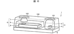
- FIG. 3 is a perspective view showing the proximity sensor model shown in FIG. 2 in a partially transparent state.
- FIG. 11 (a) shows a received light distribution on the incident surface when the distance between the top surface of the proximity sensor and the bottom surface of the housing cover is 2 mm, and
- FIG. 11 (b) shows that the distance is 4 mm. It is the light reception distribution exhibited at the incident surface when.
- FIG. 2 is a cross-sectional view illustrating a schematic configuration of the proximity sensor according to the embodiment, and illustrates a state in which the light receiving unit receives a detection result component.
- FIG. 3 is a cross-sectional view showing a schematic configuration of the proximity sensor, and shows a state in which the light receiving unit receives a crosstalk component.
- the proximity sensor 1 shown in FIGS. 2 and 3 includes a substrate 2, a light emitting unit 3, a light receiving unit 6, and a second mold unit 100.
- the substrate 2 is a substrate on which the light emitting unit 3 and the light receiving unit 6 are mounted.
- the second mold part 100 covers the light emitting part 3 and the light receiving part 6 mounted on the substrate 2, but an opening 101 and an opening 102 are provided above the light emitting part 3 and above the light receiving part 6, respectively. Is provided.
- the light emitting unit 3 emits detection light 11 which is light for detecting the presence or absence of an object to be examined (not shown).
- the light emitting unit 3 includes, for example, a light emitting element 4 that is a light source that emits infrared rays, and a first mold unit 5 that seals the light emitting element 4.
- the light receiving unit 6 receives a detection result component (a part of the reflected light) 12 in which the detection light 11 is reflected by the test object.
- the light amount of the detection result component 12 is also referred to as the detection result component 12 as in the term “crosstalk component”.
- the proximity sensor 1 detects the presence of the test object if the detection result component 12 exceeds a predetermined threshold, for example.
- the detection of the presence of the test object means the proximity of the test object to the proximity sensor 1.
- the light receiving unit 6 receives only the detection result component 12 and performs detection.
- the light receiving unit 6 normally has, together with the detection result component 12, the light reflected from the detection light 11 by, for example, the housing cover (an object other than the test object) 10, that is, a crosstalk component (part of the reflected light) 13. Is received.
- the detection light 11 passes through the housing cover 10, hits the test object, is irregularly reflected by the test object, passes through the housing cover 10, and is guided to the light receiving unit 6 as the detection result component 12. It is burned.
- the detection light 11 that could not pass through the housing cover 10 is reflected by the housing cover 10 and guided to the light receiving unit 6 as a crosstalk component 13.
- the light receiving unit 6 receives the detection result component 12 and the crosstalk component 13 as reflected light. If the reflected light exceeds a predetermined threshold, for example, it detects that there is a test object. become.
- the light receiving unit 6 has a lens 7 and a detector unit 8.
- the lens 7 condenses the detection result component 12 and the crosstalk component 13.
- the lens 7 is preferably configured such that the diameter of a light spot 13s described later is minimized when light parallel to the optical axis of the detection light 11 enters.
- the detector unit 8 is composed of one or a plurality of detectors, and has an incident surface 9 corresponding to the light receiving surfaces of all the detectors. The light collected by the lens 7 is incident on the incident surface 9.
- the housing cover 10 is a housing cover of an electronic device (such as a smartphone) on which the proximity sensor 1 is mounted.
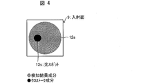
- FIG. 4 is a plan view showing an example of the distribution of the collected reflected light on the incident surface.
- the detection result component 12 occurs in the test object sufficiently far from the proximity sensor 1 than the housing cover 10 and is obtained from irregular reflection. For this reason, when the lens 7 condenses the detection result component 12, an irradiation region 12 s appears in a wide range on the incident surface 9. Note that the area of the irradiation region 12s is approximately equal to the size of the opening 102 above the light receiving unit 6 (to ensure the path of the detection result component 12 and the crosstalk component 13).
- the crosstalk component 13 is mainly light substantially parallel to the principal ray of the detection light 11 (that is, light parallel to the optical axis of the detection light) and has relatively good directivity. For this reason, if the lens 7 is configured such that the diameter of the light spot 13 s is minimized when light parallel to the optical axis of the detection light 11 is incident, the lens 7 collects the crosstalk component 13. A light spot 13 s appears locally on the incident surface 9. The area of the light spot 13s is sufficiently smaller than the area of the irradiation region 12s.
- FIGS. 1A to 1C are plan views showing a configuration in which a light spot is not formed on the incident surface.
- the proximity sensor 1 is configured so that the light spot 13 s obtained by condensing the crosstalk component 13 by the lens 7 is not formed on the incident surface 9.
- the light spot 13 s is not formed on the incident surface 9 by providing a hollow portion 14 at a position where the crosstalk component 13 is collected by the lens 7. That is, in the example shown in FIG. 1A, the lens 7 condenses the crosstalk component 13 toward the cutout portion 14.
- the light spot 13 s is incident on the incident surface 9 by providing a light shielding portion 15 that blocks the light collected by the lens 7 at the position where the crosstalk component 13 is collected by the lens 7. Is not formed. That is, in the example illustrated in FIG. 1B, the lens 7 condenses the crosstalk component 13 toward the light shielding unit 15.
- the light shielding part 15 can be comprised with the metal etc. which have a light shielding function.
- the incident surface 9 is divided into an incident surface piece 9 a and an incident surface piece 9 b, and the incident surface piece 9 a and the incident surface are arranged at a position where the crosstalk component 13 is condensed by the lens 7.
- the lens 7 condenses the crosstalk component 13 toward the gap 16.
- the crosstalk component 13 is condensed to form a light spot 13s having an area sufficiently smaller than the irradiation region 12s. For this reason, the distribution of the crosstalk component 13 is small, and it is easy to adopt a configuration in which the portion of the light spot 13 s is not used for detection by the proximity sensor 1. Therefore, it is relatively easy to ensure high detection accuracy.
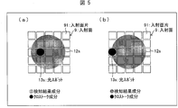
- FIGS. 5A and 5B are plan views showing a configuration in which the incidence of light on the part of the incident surface at the position where the light spot is formed is not regarded as reception of reflected light by the light receiving unit, It is a top view which shows the structure by which the entrance plane is divided
- the proximity sensor 1 After the proximity sensor 1 is mounted on an electronic device, the portion of the incident surface 9 at the position where the light spot 13s is formed (incident at the position where the light spot 13s is formed, which will be described later), according to the position of the light spot 13s.
- the proximity sensor 1 may be configured so that irradiation to the face piece 91) is not regarded as light reception by the light receiving unit 6.
- the incident surface 9 is divided into a plurality of incident surface pieces (regions) 91.
- a light spot 13s is formed around the entrance surface piece 91 in the third row from the top and the second column from the left.
- the light spot 13s is formed around the leftmost incident surface piece 91 in the third row from the top.
- Such a difference in the position of the light spot 13s is mainly caused by the relative positional relationship between the proximity sensor 1 and the housing cover 10.
- the positional relationship is known when the proximity sensor 1 is mounted on an electronic device.
- the proximity sensor 1 After the proximity sensor 1 is mounted on the electronic device, irradiation on the incident surface piece 91 at the position where the light spot 13s is formed is not regarded as light reception by the light receiving unit 6 according to the position of the light spot 13s.
- the proximity sensor 1 may be configured.
- the incident surface 9 is configured such that the incident surface piece 91 on which the light spot 13s is not formed is selected from the plurality of incident surface pieces 91 and can be detected by the proximity sensor 1.
- the configuration of the incident surface 9 shown in FIGS. 5A and 5B can be realized relatively easily by providing a plurality of detectors in the detector unit 8 and setting the incident surface piece 91 for each detector. Can do. Then, when the amount of light incident on a certain incident surface piece 91 is larger than a predetermined threshold, the detector constituting the incident surface piece 91 is not used, or the detector in a saturated state is not used. Keep it. This eliminates the need to set the proximity sensor 1 in accordance with the distribution of the crosstalk component 13 that varies due to individual differences in the housing cover 10 and / or tolerances when the proximity sensor 1 is mounted.
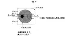
- FIG. 6 is a plan view showing a configuration in which the incident surface is divided in a direction parallel to a straight line connecting the lens and the light emitting unit.
- the light spot 13s moves substantially along a straight line 103 connecting the lens 7 and the light emitting unit 3 (amount of movement in a direction perpendicular to the straight line 103). Becomes smaller).
- the incident surface 9 is divided in a direction parallel to the straight line 103 so as to correspond to the movement of the light spot 13s substantially along the straight line 103.
- the incident surface 9 is divided in a direction parallel to the straight line 103 connecting the lens 7 and the light emitting unit 3.
- the incident surface 9 is divided into an incident surface piece 91 and incident surface pieces (large) 92a and 92b.
- Each incident surface piece 91 is divided in a direction parallel to the straight line 103.
- the light spot 13s is formed on the second incident surface piece 91 from the left, the light spot 13s moves substantially along the straight line 103 even if the distance between the housing cover 10 and the proximity sensor 1 varies. Therefore, it is formed on one or a plurality of adjacent incident surface pieces 91.
- the incident surface pieces (large) 92a and 92b are not divided in the direction parallel to the straight line 103, and are larger in size than the incident surface piece 91.
- the number of divisions of the incident surface 9 can be reduced. If the number of divisions of the incident surface 9 is reduced, the integrated circuit constituting the detector unit 8 can be simplified, so that the cost can be reduced.
- FIGS. 7A and 7B are plan views showing modifications of the configuration in which the light spot is not formed on the incident surface.
- FIG. 7A is an example in which the same configuration as in FIG. 1A is adopted when the opening shape of the opening 102 is rectangular. If the opening shape of the opening 102 is a rectangle, the irradiation region 12s has a shape close to a rectangle.
- FIG. 7B has the same configuration as that of FIG. 1C, and the incident surface pieces 9a and 9b of the incident surface 9 and the gap 16 between the incident surface piece 9a and the incident surface piece 9b. Is an example of a hexagon.
- the opening shape of the opening 102 is circular, if the incident surface pieces 9a and 9b and the gap 16 are configured in a hexagonal shape, the portion of the incident surface 9 that does not correspond to the irradiation region 12s can be reduced. For this reason, light reception by the light receiving unit 6 can be performed more efficiently.
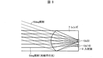
- FIG. 8 is a cross-sectional view showing a specific example of a lens.
- 0 deg irradiation optical axis parallel light
- 18 deg irradiation is light having an inclination of 18 deg with respect to the optical axis of the detection light 11 emitted from the light emitting unit 3 and is indicated by a thin solid line.
- a light spot 13s (0) is a light spot 13s obtained by condensing 0 deg irradiation (optical axis parallel light) by the lens 7, and a light spot 13s (18) is 18 deg irradiation lens.
- 7 is a light spot 13 s obtained by condensing by 7.
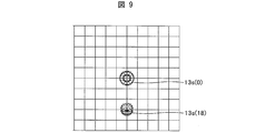
- FIG. 9 is a spot diagram of a light spot obtained from light having an inclination angle of 0 deg with respect to the optical axis of the detection light and a light spot obtained from light having an inclination angle of 18 deg.
- the incident surface 9 is a rectangle having a side of 400 ⁇ m, and the sum of all squares in the spot diagram of FIG. 9 corresponds to the rectangle.
- both the light spot 13 s (0) and the light spot 13 s (18) are sufficiently small with respect to the size of the incident surface 9.
- the light emitting element 4 an LED (Light Emitting Diode) emitting an infrared ray was used.
- the first mold part 5 a resin having a refractive index of 1.547 was used.
- the second mold part 100 a resin having infrared absorption characteristics was used.
- FIG. 11 (a) shows a received light distribution on the incident surface when the distance between the top surface of the proximity sensor and the bottom surface of the housing cover is 2 mm
- FIG. 11 (b) shows that the distance is 4 mm. It is the light reception distribution exhibited at the incident surface when.
- the light spot 13 s moves substantially along the straight line 103 according to the distance between the top surface of the proximity sensor 1 and the bottom surface of the housing cover 10.
- a proximity sensor includes a light emitting unit that emits detection light that is light for detecting the presence or absence of a test object, and the detection light that is the test object and an object (housing other than the test object).
- a proximity sensor that receives reflected light (detection result component 12 and crosstalk component 13) that is reflected by the body cover 10), the light receiving unit receiving the reflected light
- the lens has a condensing lens and an incident surface on which light collected by the lens is incident, and is obtained by the lens condensing light reflected by an object other than the test object. A light spot is not formed on the incident surface.
- the crosstalk component is condensed to form a light spot. For this reason, the distribution of the crosstalk component is small, and it is easy to adopt a configuration in which the portion of the light spot is not used for detection by the proximity sensor. Therefore, it is relatively easy to ensure high detection accuracy.
- the proximity sensor according to Aspect 2 of the present invention is the proximity sensor according to Aspect 1, wherein there is a hollow portion that is a portion where the incident surface is hollowed, and the lens is directed toward the hollow portion by an object other than the test object. Collect the reflected light.
- the proximity sensor according to aspect 3 of the present invention is the proximity sensor according to aspect 1, in which the light receiving unit includes a light shielding unit that blocks light collected by the lens, and the lens is directed toward the light shielding unit. Light reflected from an object other than the test object is collected.
- the proximity sensor according to aspect 4 of the present invention is the proximity sensor according to aspect 1, in which the incident surface is divided into two incident surface pieces, and the lens faces the gap between the two incident surface pieces. Collects light reflected by objects other than objects.
- a proximity sensor includes: a light emitting unit that emits detection light that is light for detecting the presence or absence of a test object; and the detection light is generated by the test object and an object other than the test object.
- a proximity sensor including a light receiving unit that receives reflected light that is reflected light, wherein the light receiving unit receives a lens that collects the reflected light and light collected by the lens. And a light spot obtained by the lens condensing light reflected by an object other than the test object is formed on the incident surface, and the light spot is formed. Incidence of light to the incident surface portion at a certain position is not regarded as reception of the reflected light by the light receiving unit.
- the crosstalk component is condensed to form a light spot. For this reason, the distribution of the crosstalk component is small, and it is easy to adopt a configuration in which the portion of the light spot is not used for detection by the proximity sensor. Therefore, it is relatively easy to ensure high detection accuracy.
- the incident surface is divided into a plurality of regions (incident surface pieces 91), and the light spot is formed from the plurality of regions on the incident surface. It is configured such that the detection can be performed by selecting a region that is not to be performed.
- the diversity of the crosstalk can be dealt with, and versatility for various housing covers is enhanced.
- the incident surface is divided in a direction parallel to a straight line connecting the lens and the light emitting unit.
- the number of incident surfaces can be reduced. If the number of divisions of the incident surface is reduced, the integrated circuit that constitutes the detector can be simplified, and the cost can be reduced.
- the proximity sensor according to aspect 8 of the present invention is the aspect 1 to 7, in which the lens is configured such that the diameter of the light spot is minimized when light parallel to the optical axis of the detection light is incident. Has been.
- the crosstalk component is mainly light substantially parallel to the principal ray of the detection light (that is, light parallel to the optical axis of the detection light), and has relatively good directivity. For this reason, according to said structure, when a lens condenses a crosstalk component, a light spot will appear locally on an entrance plane. Thus, the crosstalk component can be a light spot with a small diameter.
- the present invention can be used for proximity sensors.
- the present invention can be used for an infrared proximity sensor that detects the presence or absence of an object by infrared reflected light.
Landscapes
- Geophysics And Detection Of Objects (AREA)
Abstract
検知精度の向上を可能とする近接センサを提供する。クロストーク成分(13)をレンズ(7)が集光して得られた光スポット(13s)が、入射面(9)に形成されない。
Description
本発明は、近接センサに関するものである。特に、本発明は、赤外反射光によって物体の近接の有無を検知する、赤外近接センサに関するものである。
近年その市場が拡大しているスマートフォンにおいて、近接センサは、低消費電力化および各種デバイスの機能の制御に利用される。このため、スマートフォンに近接センサを搭載することが必須となっている。
上記近接センサの基本的な構造の一例が、特許文献1に開示されている。特許文献1に開示されている近接センサは、基板上に発光素子および受光素子が搭載されており、被検物により反射した光の有無に基づいて、被検物の有無を検知するものである。スマートフォンに搭載される近接センサは、特許文献1に開示されている近接センサのように、比較的コンパクトなものが多い。
ところで、近接センサをスマートフォンに搭載するとき、近接センサはスマートフォンの筐体に組み込まれるため、いわゆるクロストークの問題が発生する。本願明細書においてクロストークとは、近接センサの発光素子から発せられた光が、スマートフォン等の筐体カバー(フィルタ)にて反射し、この反射した光を受光素子が受光する現象である。特に、特許文献1に開示されている近接センサ等の簡素な構造を有する近接センサを用いる場合、クロストークの問題が顕著となる。
クロストークへの対策が施された近接センサが、特許文献2および3に開示されている。
特許文献2には、パーティショニング・デバイダおよび上側シールドにより、クロストーク成分を減衰または吸収する技術が開示されている。なお、本願明細書においてクロストーク成分とは、クロストークにより生じる光またはその光量を意味する。
特許文献3には、筒型の遮光体および可視光カット樹脂により、近接センサ内部におけるノイズ光を少なくする技術が開示されている。
また、特許文献4には、フレネルレンズとして機能する樹脂製の凸部により、発光素子および受光素子を覆う技術が開示されている。
一般に、被検物に当たった光は被検物にて乱反射する。この乱反射した光は、受光素子の受光面に平行な方向に広がるため、単位面積当たりの光量が乱反射前の光に比べて小さくなる。
特許文献2および3に開示されている技術では、受光素子に光が入射する範囲を制限しているため、受光素子が受光できる光量が小さくなってしまう。受光素子のディテクタ(検出器)のサイズを大きくすれば、受光素子が受光できる光量を増やすことができるが、クロストークの影響も大きくなる。
また、特許文献4に開示されている技術では、クロストーク成分が、円弧状の強く分布する光となる場合がある。この円弧状の光が発生する位置は、近接センサと筐体カバーとの間隔に応じて変化する。
ここで、受光素子が受光した光量を所定の閾値と比較することで、クロストーク成分を検知するケースを考える。この場合、特許文献4に開示されている技術では、検知範囲を広くする必要がある。検知範囲を広くすると、フレネルレンズの増加による検知精度の低下に起因して、種々の筐体カバーに対する汎用性が低くなる。また、近接センサを実装する際の公差によっても、上記円弧状の光が発生する位置が変化する。以上のことから、特許文献4に開示されている技術では、高い検知精度を確保することが非常に難しい。
本発明は、上記の問題に鑑みて為されたものであり、その目的は、検知精度の向上を可能とする近接センサを提供することにある。
本発明の近接センサは、上記の問題を解決するために、被検物の有無を検知するための光である検知光を発する発光部と、上記検知光が上記被検物および該被検物以外の物体にて反射された光である反射光を受光する受光部とを備えている近接センサであって、上記受光部は、上記反射光を集光するレンズと、上記レンズが集光した光が入射される入射面とを有しており、上記被検物以外の物体にて反射された光を上記レンズが集光して得られた光スポットが、上記入射面に形成されないことを特徴としている。
本発明の近接センサは、上記の問題を解決するために、被検物の有無を検知するための光である検知光を発する発光部と、上記検知光が上記被検物および該被検物以外の物体にて反射された光である反射光を受光する受光部とを備えている近接センサであって、上記受光部は、上記反射光を集光するレンズと、上記レンズが集光した光が入射される入射面とを有しており、上記被検物以外の物体にて反射された光を上記レンズが集光して得られた光スポットが、上記入射面に形成され、上記光スポットが形成される位置にある上記入射面の部分への光の入射が、上記受光部による上記反射光の受光とみなされないことを特徴としている。
本発明の一態様によれば、検知精度の向上が可能であるという効果を奏する。
〔近接センサの概略構成〕
図2は、実施の形態に係る近接センサの概略構成を示す断面図であり、受光部が検知結果成分を受光する様子を示す図である。
図2は、実施の形態に係る近接センサの概略構成を示す断面図であり、受光部が検知結果成分を受光する様子を示す図である。
図3は、上記近接センサの概略構成を示す断面図であり、受光部がクロストーク成分を受光する様子を示す図である。
図2および図3に示す近接センサ1は、基板2、発光部3、受光部6、および第2モールド部100を備えている。
基板2は、発光部3および受光部6が搭載されている基板である。
第2モールド部100は、基板2に搭載されている発光部3および受光部6を覆っているが、発光部3の上方および受光部6の上方に、それぞれ、開口部101および開口部102が設けられている。
発光部3は、被検物(図示しない)の有無を検知するための光である検知光11を発する。発光部3は、例えば赤外線を発する光源である発光素子4と、発光素子4を封止する第1モールド部5とを有している。
受光部6は、検知光11が被検物にて反射された光である検知結果成分(反射光の一部)12を受光する。なお、本願明細書では「クロストーク成分」という文言と同様に、検知結果成分12の光量についても、検知結果成分12と称する。近接センサ1は、検知結果成分12が例えば所定の閾値を超えていれば、被検物が有ることを検知する。被検物が有ることの検知が、近接センサ1に対する被検物の近接を意味する。
ここで、受光部6が、検知結果成分12のみを受光して検知を行うのが理想である。しかしながら、受光部6は通常、検知結果成分12と共に、検知光11が例えば筐体カバー(被検物以外の物体)10にて反射された光、すなわちクロストーク成分(反射光の一部)13を受光する。具体的に、検知光11は、筐体カバー10を通過して、被検物に当たり、被検物にて乱反射し、筐体カバー10を通過して、検知結果成分12として受光部6に導かれる。一方、筐体カバー10を通過できなかった検知光11は、筐体カバー10にて反射し、クロストーク成分13として受光部6に導かれる。結果、受光部6は、検知結果成分12およびクロストーク成分13を反射光として受光することになり、この反射光が例えば所定の閾値を超えていれば、被検物が有ることを検知することになる。
受光部6は、レンズ7およびディテクタ部8を有している。
レンズ7は、検知結果成分12およびクロストーク成分13を集光するものである。レンズ7は、検知光11の光軸と平行な光が入射したときに、後述する光スポット13sの径が最小となるように構成されているのが好ましい。
ディテクタ部8は、1または複数のディテクタによって構成されており、全ディテクタの受光面に相当する入射面9を有している。レンズ7が集光した光は、入射面9に入射される。
筐体カバー10は、近接センサ1が搭載されている電子機器(スマートフォン等)の筐体カバーである。
図4は、集光した反射光の、入射面における分布の一例を示す平面図である。
検知結果成分12は、筐体カバー10よりも近接センサ1から十分遠い被検物にて生じ、かつ乱反射から得られる。このため、レンズ7が検知結果成分12を集光すると、入射面9上の広い範囲に照射領域12sが現れる。なお、照射領域12sの面積は、受光部6の上方にある(検知結果成分12およびクロストーク成分13の経路を確保するための)開口部102の大きさと概ね等しい。
一方、クロストーク成分13は、検知光11の主光線(すなわち、検知光の光軸と平行な光)に対してほぼ平行な光が主であり、比較的指向性が良い。このため、検知光11の光軸と平行な光が入射したときに、光スポット13sの径が最小となるようにレンズ7が構成されていれば、レンズ7がクロストーク成分13を集光すると入射面9上に局所的に光スポット13sが現れる。光スポット13sの面積は、照射領域12sの面積に比べて十分小さくなっている。
〔実施の形態1〕
図1の(a)~(c)は、光スポットが入射面に形成されない構成を示す平面図である。
図1の(a)~(c)は、光スポットが入射面に形成されない構成を示す平面図である。
クロストーク成分13をレンズ7が集光して得られた光スポット13sが、入射面9に形成されないように、近接センサ1を構成する。
〔実施の形態2〕
図1の(a)に示す例では、レンズ7によりクロストーク成分13が集光される位置にくり抜き部14を設けることにより、光スポット13sが入射面9に形成されないようにしている。つまり、図1の(a)に示す例では、レンズ7が、くり抜き部14に向けて、クロストーク成分13を集光する。
図1の(a)に示す例では、レンズ7によりクロストーク成分13が集光される位置にくり抜き部14を設けることにより、光スポット13sが入射面9に形成されないようにしている。つまり、図1の(a)に示す例では、レンズ7が、くり抜き部14に向けて、クロストーク成分13を集光する。
〔実施の形態3〕
図1の(b)に示す例では、レンズ7によりクロストーク成分13が集光される位置に、レンズ7が集光した光を遮る遮光部15を設けることにより、光スポット13sが入射面9に形成されないようにしている。つまり、図1の(b)に示す例では、レンズ7が、遮光部15に向けて、クロストーク成分13を集光する。
図1の(b)に示す例では、レンズ7によりクロストーク成分13が集光される位置に、レンズ7が集光した光を遮る遮光部15を設けることにより、光スポット13sが入射面9に形成されないようにしている。つまり、図1の(b)に示す例では、レンズ7が、遮光部15に向けて、クロストーク成分13を集光する。
なお、遮光部15は、遮光機能を有するメタル等により構成することができる。
〔実施の形態4〕
図1の(c)に示す例では、入射面9を入射面片9aと入射面片9bとに分割し、レンズ7によりクロストーク成分13が集光される位置に、入射面片9aと入射面片9bとの間隙16を設けることにより、光スポット13sが入射面9に形成されないようにしている。つまり、図1の(c)に示す例では、レンズ7が、間隙16に向けて、クロストーク成分13を集光する。
図1の(c)に示す例では、入射面9を入射面片9aと入射面片9bとに分割し、レンズ7によりクロストーク成分13が集光される位置に、入射面片9aと入射面片9bとの間隙16を設けることにより、光スポット13sが入射面9に形成されないようにしている。つまり、図1の(c)に示す例では、レンズ7が、間隙16に向けて、クロストーク成分13を集光する。
〔実施の形態1~4の効果〕
図1の(a)~(c)に示す構成によれば、受光部6に光が入射する範囲を制限する必要が無いので、受光部6が受光できる光量の低下を抑制することができる。また、ディテクタ部8のサイズを従来から据え置きとすることが可能であるため、クロストークの影響が大きくなることを抑制することができる。
図1の(a)~(c)に示す構成によれば、受光部6に光が入射する範囲を制限する必要が無いので、受光部6が受光できる光量の低下を抑制することができる。また、ディテクタ部8のサイズを従来から据え置きとすることが可能であるため、クロストークの影響が大きくなることを抑制することができる。
また、図1の(a)~(c)に示す構成によれば、クロストーク成分13を集光して、照射領域12sより十分小さな面積の光スポット13sを形成している。このため、クロストーク成分13の分布は小さく、光スポット13sの部分を近接センサ1による検知に用いない構成を採用することが容易である。従って、高い検知精度を確保することが比較的容易である。
〔実施の形態5〕
光スポット13sが入射面9に形成される場合であっても、この光スポット13sが形成される位置にある入射面9の部分への光の入射が、受光部6による受光とみなされないように、近接センサ1を構成してもよい。これにより、光スポット13sが入射面9に形成されない場合と同様の効果が得られる。
光スポット13sが入射面9に形成される場合であっても、この光スポット13sが形成される位置にある入射面9の部分への光の入射が、受光部6による受光とみなされないように、近接センサ1を構成してもよい。これにより、光スポット13sが入射面9に形成されない場合と同様の効果が得られる。
図5の(a)および(b)は、光スポットが形成される位置にある入射面の部分への光の入射が、受光部による反射光の受光とみなされない構成を示す平面図であり、入射面が複数の領域に分割されている構成を示す平面図である。
近接センサ1を電子機器に搭載した後、光スポット13sの位置に応じて、光スポット13sが形成される位置にある入射面9の部分(後述する、光スポット13sが形成される位置にある入射面片91)への照射を、受光部6による受光とみなさないように、近接センサ1を構成すれば良い。
〔実施の形態6〕
図5の(a)および(b)に示す例では、入射面9が複数の入射面片(領域)91に分割されている。
図5の(a)および(b)に示す例では、入射面9が複数の入射面片(領域)91に分割されている。
また、図5の(a)に示す例では、上から3行目、左から2列目の入射面片91の周辺に光スポット13sが形成されている。一方、図5の(b)に示す例では、上から3行目、一番左の入射面片91の周辺に光スポット13sが形成されている。
このような光スポット13sの位置の違いは、主に近接センサ1と筐体カバー10との相対的な位置関係に起因して生じる。該位置関係は、近接センサ1を電子機器に搭載した時点で分かる。
よって、近接センサ1を電子機器に搭載した後、光スポット13sの位置に応じて、光スポット13sが形成される位置にある入射面片91への照射を、受光部6による受光とみなさないように、近接センサ1を構成すれば良い。
このように、入射面9は、複数の入射面片91から光スポット13sが形成されない入射面片91を選択して、近接センサ1による検知が可能であるように構成されているのが好ましい。
図5の(a)および(b)に示す構成によれば、クロストークの多様性に対応でき、種々の筐体カバー10に対する汎用性が高くなる。
なお、ディテクタ部8にディテクタを複数設け、該ディテクタ単位で入射面片91を設定することにより、図5の(a)および(b)に示す入射面9の構成は比較的容易に実現することができる。そして、ある入射面片91に入射される光量が所定の閾値より大きくなったときに該入射面片91を構成するディテクタを使用しない、または飽和状態にあるディテクタを使用しない、等を予め設定しておく。これにより、筐体カバー10の個体差および/または近接センサ1を実装する際の公差等によってばらつくクロストーク成分13の分布に合わせた、近接センサ1の設定が不要となる。
〔実施の形態7〕
図6は、レンズと発光部とを結ぶ直線と平行な方向に、入射面が分割されている構成を示す平面図である。
図6は、レンズと発光部とを結ぶ直線と平行な方向に、入射面が分割されている構成を示す平面図である。
筐体カバー10と近接センサ1との間隔が変動すると、光スポット13sは、レンズ7と発光部3とを結ぶ直線103に略沿って移動する(直線103に対して垂直な方向への移動量は小さくなる)。
こうした直線103に略沿った光スポット13sの移動に対応すべく、直線103と平行な方向に、入射面9を分割することが考えられる。図6に示す例において、近接センサ1は、レンズ7と発光部3とを結ぶ直線103と平行な方向に、入射面9が分割されている。
図6に示す例では、入射面9を、入射面片91と、入射面片(大)92aおよび92bとに分割している。各入射面片91は、直線103と平行な方向に分割されている。光スポット13sが左から2番目の入射面片91に形成されているが、この光スポット13sは、筐体カバー10と近接センサ1との間隔が変動しても、直線103に略沿って移動するため、1または隣接する複数の入射面片91に形成される。
一方、入射面片(大)92aおよび92bは、直線103と平行な方向への分割が見られず、サイズも入射面片91より大きい。
図6に示す例によれば、入射面9の分割数を削減することが可能となる。入射面9の分割数を削減すると、ディテクタ部8を構成する集積回路の簡素化を図ることができるため、低コスト化が可能となる。
〔変形例〕
図7の(a)および(b)は、光スポットが入射面に形成されない構成の変形例を示す平面図である。
図7の(a)および(b)は、光スポットが入射面に形成されない構成の変形例を示す平面図である。
図7の(a)に示す例は、開口部102の開口形状が矩形である場合に、図1の(a)と同様の構成を採用した例である。開口部102の開口形状が矩形であれば、照射領域12sは、矩形に近い形状となる。
図7の(b)に示す例は、図1の(c)と同様の構成であって、入射面9の入射面片9aおよび9b、ならびに入射面片9aと入射面片9bとの間隙16が六角形となっている例である。
開口部102の開口形状が円形である場合に、入射面片9aおよび9b、ならびに間隙16を六角形状に構成すると、照射領域12sに該当しない入射面9の部分を削減することができる。このため、受光部6による受光をより効率的に行うことが可能となる。
〔レンズの構成例〕
図8は、レンズの具体例を示す断面図である。
図8は、レンズの具体例を示す断面図である。
図8において「0deg照射(光軸平行光)」とは、発光部3が発する検知光11の光軸に対する傾斜が0degの光、すなわち、該光軸と平行な光であり、太い実線で示している。一方、図8において「18deg照射」とは、発光部3が発する検知光11の光軸に対する傾斜が18degの光であり、細い実線で示している。
また、図8において、光スポット13s(0)は、0deg照射(光軸平行光)をレンズ7により集光して得られる光スポット13sであり、光スポット13s(18)は、18deg照射をレンズ7により集光して得られる光スポット13sである。
なお、以下の説明では、レンズ7に入射する光の波長λ=935nmとし、屈折率n=1.547、曲率半径R=0.3mm、レンズ厚(レンズ頂点からレンズ底面までの距離)t=0.67mmのレンズ7を用いている。
〔スポットダイアグラム〕
図9は、検知光の光軸に対する傾斜角度が0degの光から得られる光スポットと、同傾斜角度が18degの光から得られる光スポットとのスポットダイアグラムである。
図9は、検知光の光軸に対する傾斜角度が0degの光から得られる光スポットと、同傾斜角度が18degの光から得られる光スポットとのスポットダイアグラムである。
なお、入射面9は1辺400μmの矩形であり、図9のスポットダイアグラムの全マス目の合計が該矩形に対応するものとする。
光スポット13s(0)および光スポット13s(18)はいずれも、入射面9の大きさに対して十分小さくなっていることが分かる。
〔近接センサのモデルを用いた検証〕
近接センサ1のモデル(図10参照)を用いた検証を実施した。
近接センサ1のモデル(図10参照)を用いた検証を実施した。
なお、筐体カバー10は、屈折率n=1.51、厚みt=0.7mmとした。そして、上記検証は、近接センサ1の天面と筐体カバー10の底面との間隔が2mmである場合と4mmである場合との2パターンにて、光学シミュレーションにより実施した。
発光素子4として、赤外線を発するLED(Light Emitting Diode:発光ダイオード)を用いた。第1モールド部5として、屈折率1.547の樹脂を用いた。第2モールド部100として、赤外線吸収特性を有する樹脂を用いた。
上記赤外線の配光特性を、I(θ)=Io・(cosθ)^20とした。
図11の(a)は、近接センサの天面と筐体カバーの底面との間隔が2mmである場合に入射面にて呈する受光分布であり、図11の(b)は、同間隔が4mmである場合に入射面にて呈する受光分布である。
図11の(a)および(b)から、検知結果成分12は照射領域12sとして広い範囲に分布する一方、クロストーク成分13は光スポット13sとして狭い範囲に強く分布することが明らかになった。
また、近接センサ1の天面と筐体カバー10の底面との間隔に応じて、光スポット13sが直線103に略沿って移動することが分かった。
以上のことから、入射面9を分割し、光スポット13sが形成される位置にある入射面9の部分を、近接センサ1による検知に用いないことが有効であるということが分かった。そして、光スポット13sが形成されない入射面片91(図5の(a)および(b)参照)を選択することが有効であるということが分かった。
〔まとめ〕
本発明の態様1に係る近接センサは、被検物の有無を検知するための光である検知光を発する発光部と、上記検知光が上記被検物および該被検物以外の物体(筐体カバー10)にて反射された光である反射光(検知結果成分12およびクロストーク成分13)を受光する受光部とを備えている近接センサであって、上記受光部は、上記反射光を集光するレンズと、上記レンズが集光した光が入射される入射面とを有しており、上記被検物以外の物体にて反射された光を上記レンズが集光して得られた光スポットが、上記入射面に形成されない。
本発明の態様1に係る近接センサは、被検物の有無を検知するための光である検知光を発する発光部と、上記検知光が上記被検物および該被検物以外の物体(筐体カバー10)にて反射された光である反射光(検知結果成分12およびクロストーク成分13)を受光する受光部とを備えている近接センサであって、上記受光部は、上記反射光を集光するレンズと、上記レンズが集光した光が入射される入射面とを有しており、上記被検物以外の物体にて反射された光を上記レンズが集光して得られた光スポットが、上記入射面に形成されない。
上記の構成によれば、受光部に光が入射する範囲を制限する必要が無いので、受光部が受光できる光量の低下を抑制することができる。また、ディテクタのサイズを従来から据え置きとすることが可能であるため、クロストークの影響が大きくなることを抑制することができる。
また、上記の構成によれば、クロストーク成分を集光して、光スポットを形成している。このため、クロストーク成分の分布は小さく、光スポットの部分を近接センサによる検知に用いない構成を採用することが容易である。従って、高い検知精度を確保することが比較的容易である。
本発明の態様2に係る近接センサは、上記態様1において、上記入射面をくり抜いた部分であるくり抜き部があり、上記レンズが、上記くり抜き部に向けて、上記被検物以外の物体にて反射された光を集光する。
本発明の態様3に係る近接センサは、上記態様1において、上記受光部は、上記レンズが集光した光を遮る遮光部を有しており、上記レンズが、上記遮光部に向けて、上記被検物以外の物体にて反射された光を集光する。
本発明の態様4に係る近接センサは、上記態様1において、上記入射面が2つの入射面片に分割されており、上記レンズが、2つの上記入射面片の間隙に向けて、上記被検物以外の物体にて反射された光を集光する。
本発明の態様5に係る近接センサは、被検物の有無を検知するための光である検知光を発する発光部と、上記検知光が上記被検物および該被検物以外の物体にて反射された光である反射光を受光する受光部とを備えている近接センサであって、上記受光部は、上記反射光を集光するレンズと、上記レンズが集光した光が入射される入射面とを有しており、上記被検物以外の物体にて反射された光を上記レンズが集光して得られた光スポットが、上記入射面に形成され、上記光スポットが形成される位置にある上記入射面の部分への光の入射が、上記受光部による上記反射光の受光とみなされない。
上記の構成によれば、受光部に光が入射する範囲を制限する必要が無いので、受光部が受光できる光量の低下を抑制することができる。また、ディテクタのサイズを従来から据え置きとすることが可能であるため、クロストークの影響が大きくなることを抑制することができる。
また、上記の構成によれば、クロストーク成分を集光して、光スポットを形成している。このため、クロストーク成分の分布は小さく、光スポットの部分を近接センサによる検知に用いない構成を採用することが容易である。従って、高い検知精度を確保することが比較的容易である。
本発明の態様6に係る近接センサは、上記態様5において、上記入射面が複数の領域(入射面片91)に分割されており、上記入射面は、上記複数の領域から上記光スポットが形成されない領域を選択して上記検知が可能であるように構成されている。
上記の構成によれば、クロストークの多様性に対応でき、種々の筐体カバーに対する汎用性が高くなる。
本発明の態様7に係る近接センサは、上記態様6において、上記レンズと上記発光部とを結ぶ直線と平行な方向に、上記入射面が分割されている。
上記の構成によれば、入射面の分割数を削減することが可能となる。入射面の分割数を削減すると、ディテクタを構成する集積回路の簡素化を図ることができるため、低コスト化が可能となる。
本発明の態様8に係る近接センサは、上記態様1から7において、上記レンズは、上記検知光の光軸と平行な光が入射したときに、上記光スポットの径が最小となるように構成されている。
クロストーク成分は、検知光の主光線(すなわち、検知光の光軸と平行な光)に対してほぼ平行な光が主であり、比較的指向性が良い。このため、上記の構成によれば、レンズがクロストーク成分を集光すると入射面上に局所的に光スポットが現れる。こうして、クロストーク成分を、径の小さな光スポットとすることができる。
本発明は上述した各実施形態に限定されるものではなく、請求項に示した範囲で種々の変更が可能であり、異なる実施形態にそれぞれ開示された技術的手段を適宜組み合わせて得られる実施形態についても本発明の技術的範囲に含まれる。さらに、各実施形態にそれぞれ開示された技術的手段を組み合わせることにより、新しい技術的特徴を形成することができる。
本発明は、近接センサに利用することができる。特に、本発明は、赤外反射光によって物体の近接の有無を検知する、赤外近接センサに利用することができる。
1 近接センサ
3 発光部
6 受光部
7 レンズ
9 入射面
10 筐体カバー(被検物以外の物体)
11 検知光
12 検知結果成分(反射光の一部)
13 クロストーク成分(反射光の一部)
13s 光スポット
14 くり抜き部
15 遮光部
16 間隙
91 入射面片(領域)
102 開口部
103 直線
3 発光部
6 受光部
7 レンズ
9 入射面
10 筐体カバー(被検物以外の物体)
11 検知光
12 検知結果成分(反射光の一部)
13 クロストーク成分(反射光の一部)
13s 光スポット
14 くり抜き部
15 遮光部
16 間隙
91 入射面片(領域)
102 開口部
103 直線
Claims (5)
- 被検物の有無を検知するための光である検知光を発する発光部と、
上記検知光が上記被検物および該被検物以外の物体にて反射された光である反射光を受光する受光部とを備えている近接センサであって、
上記受光部は、
上記反射光を集光するレンズと、
上記レンズが集光した光が入射される入射面とを有しており、
上記被検物以外の物体にて反射された光を上記レンズが集光して得られた光スポットが、上記入射面に形成されないことを特徴とする近接センサ。 - 被検物の有無を検知するための光である検知光を発する発光部と、
上記検知光が上記被検物および該被検物以外の物体にて反射された光である反射光を受光する受光部とを備えている近接センサであって、
上記受光部は、
上記反射光を集光するレンズと、
上記レンズが集光した光が入射される入射面とを有しており、
上記被検物以外の物体にて反射された光を上記レンズが集光して得られた光スポットが、上記入射面に形成され、
上記光スポットが形成される位置にある上記入射面の部分への光の入射が、上記受光部による上記反射光の受光とみなされないことを特徴とする近接センサ。 - 上記入射面が複数の領域に分割されており、
上記入射面は、上記複数の領域から上記光スポットが形成されない領域を選択して上記検知が可能であるように構成されていることを特徴とする請求項2に記載の近接センサ。 - 上記レンズと上記発光部とを結ぶ直線と平行な方向に、上記入射面が分割されていることを特徴とする請求項3に記載の近接センサ。
- 上記レンズは、上記検知光の光軸と平行な光が入射したときに、上記光スポットの径が最小となるように構成されていることを特徴とする請求項1から4のいずれか1項に記載の近接センサ。
Applications Claiming Priority (2)
| Application Number | Priority Date | Filing Date | Title |
|---|---|---|---|
| JP2013-171414 | 2013-08-21 | ||
| JP2013171414 | 2013-08-21 |
Publications (1)
| Publication Number | Publication Date |
|---|---|
| WO2015025591A1 true WO2015025591A1 (ja) | 2015-02-26 |
Family
ID=52483376
Family Applications (1)
| Application Number | Title | Priority Date | Filing Date |
|---|---|---|---|
| PCT/JP2014/065365 Ceased WO2015025591A1 (ja) | 2013-08-21 | 2014-06-10 | 近接センサ |
Country Status (1)
| Country | Link |
|---|---|
| WO (1) | WO2015025591A1 (ja) |
Citations (4)
| Publication number | Priority date | Publication date | Assignee | Title |
|---|---|---|---|---|
| JPH0567418A (ja) * | 1991-09-06 | 1993-03-19 | Omron Corp | 光センサ |
| JPH11166979A (ja) * | 1997-12-04 | 1999-06-22 | Nabco Ltd | 物体検出装置の実効検出エリア設定方法及び実効検出エリア設定システム |
| JP2007206059A (ja) * | 2005-12-16 | 2007-08-16 | Sick Ag | 光電装置及び光電装置の動作方法 |
| JP2011208480A (ja) * | 2010-03-30 | 2011-10-20 | Kyokko Denki Kk | 自動ドア用物体検出装置 |
-
2014
- 2014-06-10 WO PCT/JP2014/065365 patent/WO2015025591A1/ja not_active Ceased
Patent Citations (4)
| Publication number | Priority date | Publication date | Assignee | Title |
|---|---|---|---|---|
| JPH0567418A (ja) * | 1991-09-06 | 1993-03-19 | Omron Corp | 光センサ |
| JPH11166979A (ja) * | 1997-12-04 | 1999-06-22 | Nabco Ltd | 物体検出装置の実効検出エリア設定方法及び実効検出エリア設定システム |
| JP2007206059A (ja) * | 2005-12-16 | 2007-08-16 | Sick Ag | 光電装置及び光電装置の動作方法 |
| JP2011208480A (ja) * | 2010-03-30 | 2011-10-20 | Kyokko Denki Kk | 自動ドア用物体検出装置 |
Similar Documents
| Publication | Publication Date | Title |
|---|---|---|
| KR101659549B1 (ko) | 광 센서 | |
| EP2672295B1 (en) | Photoelectric sensor | |
| CN103620799B (zh) | 反射型光电传感器 | |
| US10422876B2 (en) | Optical sensor arrangement | |
| US11662462B2 (en) | Proximity sensor for alleviating crosstalk and electronic device using the same | |
| CN114706258B (zh) | 多光源的光机结构 | |
| JP2016162666A5 (ja) | ||
| JPH11248629A (ja) | 光散乱式粒子検知センサ | |
| JP6552052B2 (ja) | トナー付着量センサ | |
| WO2015025593A1 (ja) | 近接センサ | |
| KR101710534B1 (ko) | 광학식 센서를 위한 광학계 및 이를 포함하는 센서 | |
| WO2019184789A1 (zh) | 激光投射装置及移动终端 | |
| JP5251641B2 (ja) | 光電センサ | |
| KR20160119178A (ko) | 근접 검출용 광학 센서 장치 | |
| CN107563317A (zh) | 感光模组及感光装置 | |
| US11674842B2 (en) | Optical sensor arrangement | |
| WO2015025591A1 (ja) | 近接センサ | |
| KR101723895B1 (ko) | 터치 신호 검출의 정확성이 향상된 적외선 터치스크린 시스템 | |
| JP6584201B2 (ja) | 回帰反射形光電センサ | |
| TWI359936B (ja) | ||
| US20120188773A1 (en) | Encoding Device and a Method of Encoding | |
| WO2015146429A1 (ja) | パーティクル計数装置 | |
| JP7703725B1 (ja) | 光学センサ | |
| KR200485081Y1 (ko) | 투광커버를 구비한 스마트펜 | |
| JP2007003348A (ja) | 回帰反射型光電センサ |
Legal Events
| Date | Code | Title | Description |
|---|---|---|---|
| 121 | Ep: the epo has been informed by wipo that ep was designated in this application |
Ref document number: 14838118 Country of ref document: EP Kind code of ref document: A1 |
|
| NENP | Non-entry into the national phase |
Ref country code: DE |
|
| 122 | Ep: pct application non-entry in european phase |
Ref document number: 14838118 Country of ref document: EP Kind code of ref document: A1 |
|
| NENP | Non-entry into the national phase |
Ref country code: JP |