WO2015019543A1 - 表示パネル及び表示パネルの駆動方法 - Google Patents
表示パネル及び表示パネルの駆動方法 Download PDFInfo
- Publication number
- WO2015019543A1 WO2015019543A1 PCT/JP2014/003565 JP2014003565W WO2015019543A1 WO 2015019543 A1 WO2015019543 A1 WO 2015019543A1 JP 2014003565 W JP2014003565 W JP 2014003565W WO 2015019543 A1 WO2015019543 A1 WO 2015019543A1
- Authority
- WO
- WIPO (PCT)
- Prior art keywords
- power supply
- voltage
- capacitor
- switch element
- inductor
- Prior art date
- Legal status (The legal status is an assumption and is not a legal conclusion. Google has not performed a legal analysis and makes no representation as to the accuracy of the status listed.)
- Ceased
Links
Images







Classifications
-
- G—PHYSICS
- G09—EDUCATION; CRYPTOGRAPHY; DISPLAY; ADVERTISING; SEALS
- G09G—ARRANGEMENTS OR CIRCUITS FOR CONTROL OF INDICATING DEVICES USING STATIC MEANS TO PRESENT VARIABLE INFORMATION
- G09G3/00—Control arrangements or circuits, of interest only in connection with visual indicators other than cathode-ray tubes
- G09G3/20—Control arrangements or circuits, of interest only in connection with visual indicators other than cathode-ray tubes for presentation of an assembly of a number of characters, e.g. a page, by composing the assembly by combination of individual elements arranged in a matrix no fixed position being assigned to or needed to be assigned to the individual characters or partial characters
- G09G3/22—Control arrangements or circuits, of interest only in connection with visual indicators other than cathode-ray tubes for presentation of an assembly of a number of characters, e.g. a page, by composing the assembly by combination of individual elements arranged in a matrix no fixed position being assigned to or needed to be assigned to the individual characters or partial characters using controlled light sources
- G09G3/30—Control arrangements or circuits, of interest only in connection with visual indicators other than cathode-ray tubes for presentation of an assembly of a number of characters, e.g. a page, by composing the assembly by combination of individual elements arranged in a matrix no fixed position being assigned to or needed to be assigned to the individual characters or partial characters using controlled light sources using electroluminescent panels
-
- G—PHYSICS
- G09—EDUCATION; CRYPTOGRAPHY; DISPLAY; ADVERTISING; SEALS
- G09G—ARRANGEMENTS OR CIRCUITS FOR CONTROL OF INDICATING DEVICES USING STATIC MEANS TO PRESENT VARIABLE INFORMATION
- G09G3/00—Control arrangements or circuits, of interest only in connection with visual indicators other than cathode-ray tubes
- G09G3/20—Control arrangements or circuits, of interest only in connection with visual indicators other than cathode-ray tubes for presentation of an assembly of a number of characters, e.g. a page, by composing the assembly by combination of individual elements arranged in a matrix no fixed position being assigned to or needed to be assigned to the individual characters or partial characters
- G09G3/22—Control arrangements or circuits, of interest only in connection with visual indicators other than cathode-ray tubes for presentation of an assembly of a number of characters, e.g. a page, by composing the assembly by combination of individual elements arranged in a matrix no fixed position being assigned to or needed to be assigned to the individual characters or partial characters using controlled light sources
- G09G3/30—Control arrangements or circuits, of interest only in connection with visual indicators other than cathode-ray tubes for presentation of an assembly of a number of characters, e.g. a page, by composing the assembly by combination of individual elements arranged in a matrix no fixed position being assigned to or needed to be assigned to the individual characters or partial characters using controlled light sources using electroluminescent panels
- G09G3/32—Control arrangements or circuits, of interest only in connection with visual indicators other than cathode-ray tubes for presentation of an assembly of a number of characters, e.g. a page, by composing the assembly by combination of individual elements arranged in a matrix no fixed position being assigned to or needed to be assigned to the individual characters or partial characters using controlled light sources using electroluminescent panels semiconductive, e.g. using light-emitting diodes [LED]
- G09G3/3208—Control arrangements or circuits, of interest only in connection with visual indicators other than cathode-ray tubes for presentation of an assembly of a number of characters, e.g. a page, by composing the assembly by combination of individual elements arranged in a matrix no fixed position being assigned to or needed to be assigned to the individual characters or partial characters using controlled light sources using electroluminescent panels semiconductive, e.g. using light-emitting diodes [LED] organic, e.g. using organic light-emitting diodes [OLED]
- G09G3/3225—Control arrangements or circuits, of interest only in connection with visual indicators other than cathode-ray tubes for presentation of an assembly of a number of characters, e.g. a page, by composing the assembly by combination of individual elements arranged in a matrix no fixed position being assigned to or needed to be assigned to the individual characters or partial characters using controlled light sources using electroluminescent panels semiconductive, e.g. using light-emitting diodes [LED] organic, e.g. using organic light-emitting diodes [OLED] using an active matrix
- G09G3/3233—Control arrangements or circuits, of interest only in connection with visual indicators other than cathode-ray tubes for presentation of an assembly of a number of characters, e.g. a page, by composing the assembly by combination of individual elements arranged in a matrix no fixed position being assigned to or needed to be assigned to the individual characters or partial characters using controlled light sources using electroluminescent panels semiconductive, e.g. using light-emitting diodes [LED] organic, e.g. using organic light-emitting diodes [OLED] using an active matrix with pixel circuitry controlling the current through the light-emitting element
-
- H—ELECTRICITY
- H02—GENERATION; CONVERSION OR DISTRIBUTION OF ELECTRIC POWER
- H02M—APPARATUS FOR CONVERSION BETWEEN AC AND AC, BETWEEN AC AND DC, OR BETWEEN DC AND DC, AND FOR USE WITH MAINS OR SIMILAR POWER SUPPLY SYSTEMS; CONVERSION OF DC OR AC INPUT POWER INTO SURGE OUTPUT POWER; CONTROL OR REGULATION THEREOF
- H02M3/00—Conversion of DC power input into DC power output
- H02M3/02—Conversion of DC power input into DC power output without intermediate conversion into AC
- H02M3/04—Conversion of DC power input into DC power output without intermediate conversion into AC by static converters
- H02M3/10—Conversion of DC power input into DC power output without intermediate conversion into AC by static converters using discharge tubes with control electrode or semiconductor devices with control electrode
- H02M3/145—Conversion of DC power input into DC power output without intermediate conversion into AC by static converters using discharge tubes with control electrode or semiconductor devices with control electrode using devices of a triode or transistor type requiring continuous application of a control signal
- H02M3/155—Conversion of DC power input into DC power output without intermediate conversion into AC by static converters using discharge tubes with control electrode or semiconductor devices with control electrode using devices of a triode or transistor type requiring continuous application of a control signal using semiconductor devices only
- H02M3/156—Conversion of DC power input into DC power output without intermediate conversion into AC by static converters using discharge tubes with control electrode or semiconductor devices with control electrode using devices of a triode or transistor type requiring continuous application of a control signal using semiconductor devices only with automatic control of output voltage or current, e.g. switching regulators
- H02M3/158—Conversion of DC power input into DC power output without intermediate conversion into AC by static converters using discharge tubes with control electrode or semiconductor devices with control electrode using devices of a triode or transistor type requiring continuous application of a control signal using semiconductor devices only with automatic control of output voltage or current, e.g. switching regulators including plural semiconductor devices as final control devices for a single load
-
- G—PHYSICS
- G09—EDUCATION; CRYPTOGRAPHY; DISPLAY; ADVERTISING; SEALS
- G09G—ARRANGEMENTS OR CIRCUITS FOR CONTROL OF INDICATING DEVICES USING STATIC MEANS TO PRESENT VARIABLE INFORMATION
- G09G2300/00—Aspects of the constitution of display devices
- G09G2300/08—Active matrix structure, i.e. with use of active elements, inclusive of non-linear two terminal elements, in the pixels together with light emitting or modulating elements
- G09G2300/0809—Several active elements per pixel in active matrix panels
- G09G2300/0842—Several active elements per pixel in active matrix panels forming a memory circuit, e.g. a dynamic memory with one capacitor
-
- G—PHYSICS
- G09—EDUCATION; CRYPTOGRAPHY; DISPLAY; ADVERTISING; SEALS
- G09G—ARRANGEMENTS OR CIRCUITS FOR CONTROL OF INDICATING DEVICES USING STATIC MEANS TO PRESENT VARIABLE INFORMATION
- G09G2330/00—Aspects of power supply; Aspects of display protection and defect management
- G09G2330/02—Details of power systems and of start or stop of display operation
- G09G2330/021—Power management, e.g. power saving
-
- G—PHYSICS
- G09—EDUCATION; CRYPTOGRAPHY; DISPLAY; ADVERTISING; SEALS
- G09G—ARRANGEMENTS OR CIRCUITS FOR CONTROL OF INDICATING DEVICES USING STATIC MEANS TO PRESENT VARIABLE INFORMATION
- G09G2330/00—Aspects of power supply; Aspects of display protection and defect management
- G09G2330/02—Details of power systems and of start or stop of display operation
- G09G2330/028—Generation of voltages supplied to electrode drivers in a matrix display other than LCD
-
- H—ELECTRICITY
- H02—GENERATION; CONVERSION OR DISTRIBUTION OF ELECTRIC POWER
- H02M—APPARATUS FOR CONVERSION BETWEEN AC AND AC, BETWEEN AC AND DC, OR BETWEEN DC AND DC, AND FOR USE WITH MAINS OR SIMILAR POWER SUPPLY SYSTEMS; CONVERSION OF DC OR AC INPUT POWER INTO SURGE OUTPUT POWER; CONTROL OR REGULATION THEREOF
- H02M1/00—Details of apparatus for conversion
- H02M1/0048—Circuits or arrangements for reducing losses
-
- H—ELECTRICITY
- H02—GENERATION; CONVERSION OR DISTRIBUTION OF ELECTRIC POWER
- H02M—APPARATUS FOR CONVERSION BETWEEN AC AND AC, BETWEEN AC AND DC, OR BETWEEN DC AND DC, AND FOR USE WITH MAINS OR SIMILAR POWER SUPPLY SYSTEMS; CONVERSION OF DC OR AC INPUT POWER INTO SURGE OUTPUT POWER; CONTROL OR REGULATION THEREOF
- H02M3/00—Conversion of DC power input into DC power output
- H02M3/02—Conversion of DC power input into DC power output without intermediate conversion into AC
- H02M3/04—Conversion of DC power input into DC power output without intermediate conversion into AC by static converters
- H02M3/06—Conversion of DC power input into DC power output without intermediate conversion into AC by static converters using resistors or capacitors, e.g. potential divider
- H02M3/07—Conversion of DC power input into DC power output without intermediate conversion into AC by static converters using resistors or capacitors, e.g. potential divider using capacitors charged and discharged alternately by semiconductor devices with control electrode, e.g. charge pumps
-
- Y—GENERAL TAGGING OF NEW TECHNOLOGICAL DEVELOPMENTS; GENERAL TAGGING OF CROSS-SECTIONAL TECHNOLOGIES SPANNING OVER SEVERAL SECTIONS OF THE IPC; TECHNICAL SUBJECTS COVERED BY FORMER USPC CROSS-REFERENCE ART COLLECTIONS [XRACs] AND DIGESTS
- Y02—TECHNOLOGIES OR APPLICATIONS FOR MITIGATION OR ADAPTATION AGAINST CLIMATE CHANGE
- Y02B—CLIMATE CHANGE MITIGATION TECHNOLOGIES RELATED TO BUILDINGS, e.g. HOUSING, HOUSE APPLIANCES OR RELATED END-USER APPLICATIONS
- Y02B70/00—Technologies for an efficient end-user side electric power management and consumption
- Y02B70/10—Technologies improving the efficiency by using switched-mode power supplies [SMPS], i.e. efficient power electronics conversion e.g. power factor correction or reduction of losses in power supplies or efficient standby modes
Definitions
- one aspect of the display panel includes a plurality of light emitting elements and an input power supply voltage, and a first power supply voltage and a variable second power used for light emission of the plurality of light emitting elements.
- a power supply unit that generates a power supply voltage, a first power supply line that transmits the first power supply voltage from the power supply unit to the plurality of light emitting elements, and a second power supply voltage that is transmitted from the power supply unit to the plurality of light emitting elements.
- power is recovered from the inductor to the capacitor and regenerated to charge the parasitic capacitance of the power supply line, so that power loss can be reduced.
- a first switch element that switches between conduction and non-conduction between the second terminal of the inductor and one of the input terminals
- a second switch element that switches between conduction and non-conduction between the second terminal of the inductor and the other of the input terminals
- a capacitor having a first electrode connected to a constant voltage
- the switching control unit that controls the inductor.
- a third switch element that switches between conduction and non-conduction between the second terminal of the capacitor and the second electrode of the capacitor, and the switching control unit has the second power supply voltage set to the first voltage.
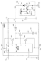
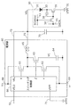
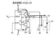
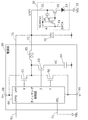
- the power supply unit 60 generates the power supply voltage VTFT and the power supply voltage VEL from the input power supply voltages V ⁇ and V + applied to the input terminals 68 and 69.
- the power supply voltage VTFT and the power supply voltage VEL are supplied to the power supply terminals 31 and 32 of the pixel unit 30 via the power supply lines 71 and 72, respectively.
- the power supply voltage VTFT is, for example, a fixed voltage.
- the power supply voltage VEL is adjusted to be equal to the voltage VEL0 of the signal line 51 by the switching regulator circuit.
- the signal line 51 is instructed with at least two kinds of voltages VEL0 for the purpose of controlling light emission and non-light emission of the pixel unit 30.
- the fluctuation of the threshold voltage Vth of the driving transistor is suppressed by bringing the driving transistor into a conducting state once prior to the light emission step.
- luminance errors for example, tailing when the window is scroll-displayed
- display quality can be improved.
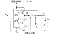
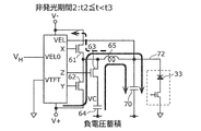
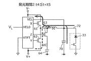
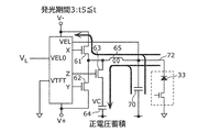
- the switching control unit 66 brings the transistor 63 into a conductive state by setting only the gate signal Z among the gate signals X, Y, and Z to a high level.
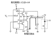
- the parasitic capacitance 70 of the second power supply line 72 is charged with the voltage charged in the capacitor 64, and the power supply voltage VEL rises without consuming power from the input power supply voltage.
- the power supply voltage VEL is equal to or higher than the voltage obtained by adding the threshold voltage of the organic EL element 33 to the voltage VL , the organic EL element 33 can emit light.
Landscapes
- Engineering & Computer Science (AREA)
- Physics & Mathematics (AREA)
- Computer Hardware Design (AREA)
- General Physics & Mathematics (AREA)
- Theoretical Computer Science (AREA)
- Power Engineering (AREA)
- Control Of Indicators Other Than Cathode Ray Tubes (AREA)
- Control Of El Displays (AREA)
- Electroluminescent Light Sources (AREA)
Abstract
Description
なお、包括的又は具体的な態様は、システム、集積回路、コンピュータプログラム又はコンピュータ読み取り可能なCD-ROMなどの記録媒体で実現されてもよい。また、包括的又は具体的な態様は、システム、方法、集積回路、コンピュータプログラム又は記録媒体の任意な組み合わせで実現されてもよい。
本発明者は、背景技術の欄において記載した、表示パネルにおける電源線の寄生容量に起因する電力ロスに関し、以下の問題が生じることを見出した。
20 表示部
30 画素部
31,32 電源端子
33 有機EL素子(発光素子)
34 スイッチングトランジスタ
35 駆動トランジスタ
36 保持容量
40 信号線駆動部
41 データ信号線
42 走査線駆動部
43 走査信号線
50 パネル制御部
51 信号線
60 電源部
61~63 トランジスタ(スイッチ素子)
64 キャパシタ
65 インダクタ
66 スイッチング制御部
70 寄生容量
71,72 電源線
73 センス線
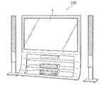
100 テレビジョンセット
Claims (6)
- 複数の発光素子と、
入力電源電圧から、前記複数の発光素子の発光に用いられる第1電源電圧及び可変の第2電源電圧を生成する電源部と、
前記第1電源電圧を前記電源部から前記複数の発光素子へ伝達する第1電源線と、
前記第2電源電圧を前記電源部から前記複数の発光素子へ伝達する第2電源線と、を備え、
前記電源部は、
前記入力電源電圧が印加される一対の入力端子と、
スイッチング制御部と、
第1端子が前記第2電源線に接続されるインダクタと、
前記スイッチング制御部によって制御され、前記インダクタの第2端子と、前記入力端子の一方との導通及び非導通を切り換える第1スイッチ素子と、
前記スイッチング制御部によって制御され、前記インダクタの前記第2端子と、前記入力端子の他方との導通及び非導通を切り換える第2スイッチ素子と、
第1電極が一定電圧に接続されるキャパシタと、
前記スイッチング制御部によって制御され、前記インダクタの前記第2端子と、前記キャパシタの第2電極との導通及び非導通を切り換える第3スイッチ素子と、
を有し、
前記スイッチング制御部は、
前記第2電源電圧が第1電圧に設定されているとき、前記インダクタに流れる電流で前記キャパシタに電荷を蓄積するために、前記第1スイッチ素子及び前記第2スイッチ素子の何れか一方と前記第3スイッチ素子とを排他的に導通状態にし、
前記第2電源電圧を前記第1電圧から第2電圧に変更するとき、前記キャパシタに蓄積された電荷で前記第2電源線の寄生容量を充電するために、前記第3スイッチ素子を導通状態にする、
表示パネル。 - 前記スイッチング制御部は、
前記発光素子の発光期間において、前記インダクタに流れる電流で前記キャパシタに電荷を蓄積するために、前記第2スイッチ素子と前記第3スイッチ素子とを排他的に導通状態にし、
前記発光素子の非発光期間になったときに、前記キャパシタに蓄積された電荷で前記第2電源線の寄生容量を充電するために、前記第3スイッチ素子を導通状態にする、
請求項1に記載の表示パネル。 - 前記スイッチング制御部は、
前記発光素子の非発光期間において、前記インダクタに流れる電流で前記キャパシタに電荷を蓄積するために、前記第2スイッチ素子と前記第3スイッチ素子とを排他的に導通状態にし、
前記発光素子の発光期間になったときに、前記キャパシタに蓄積された電荷で前記第2電源線の寄生容量を充電するために、前記第3スイッチ素子を導通状態にする、
請求項1に記載の表示パネル。 - 表示パネルの駆動方法であって、
前記表示パネルは、
複数の発光素子と、
入力電源電圧から、前記複数の発光素子の発光に用いられる第1電源電圧及び可変の第2電源電圧を生成する電源部と、
前記第1電源電圧を前記電源部から前記複数の発光素子へ伝達する第1電源線と、
前記第2電源電圧を前記電源部から前記複数の発光素子へ伝達する第2電源線と、を備え、
前記電源部は、
前記入力電源電圧が印加される一対の入力端子と、
スイッチング制御部と、
第1端子が前記第2電源線に接続されるインダクタと、
前記スイッチング制御部によって制御され、前記インダクタの第2端子と、前記入力端子の一方との導通及び非導通を切り換える第1スイッチ素子と、
前記スイッチング制御部によって制御され、前記インダクタの前記第2端子と、前記入力端子の他方との導通及び非導通を切り換える第2スイッチ素子と、
第1電極が一定電圧に接続されるキャパシタと、
前記スイッチング制御部によって制御され、前記インダクタの前記第2端子と、前記キャパシタの第2電極との導通及び非導通を切り換える第3スイッチ素子と、
を有し、
前記駆動方法は、
前記第2電源電圧が第1電圧に設定されているとき、前記インダクタに流れる電流で前記キャパシタに電荷を蓄積するために、前記第1スイッチ素子及び前記第2スイッチ素子の何れか一方と前記第3スイッチ素子とを排他的に導通状態にすることと、
前記第2電源電圧を前記第1電圧から第2電圧に変更するとき、前記キャパシタに蓄積された電荷で前記第2電源線の寄生容量を充電するために、前記第3スイッチ素子を導通状態にすることと、を含む、
表示パネルの駆動方法。 - 前記発光素子の発光期間において、前記インダクタに流れる電流で前記キャパシタに電荷を蓄積するために、前記第2スイッチ素子と前記第3スイッチ素子とを排他的に導通状態にし、
前記発光素子の非発光期間になったときに、前記キャパシタに蓄積された電荷で前記第2電源線の寄生容量を充電するために、前記第3スイッチ素子を導通状態にする、
請求項4に記載の表示パネルの駆動方法。 - 前記発光素子の非発光期間において、前記インダクタに流れる電流で前記キャパシタに電荷を蓄積するために、前記第2スイッチ素子と前記第3スイッチ素子とを排他的に導通状態にし、
前記発光素子の発光期間になったときに、前記キャパシタに蓄積された電荷で前記第2電源線の寄生容量を充電するために、前記第3スイッチ素子を導通状態にする、
請求項4に記載の表示パネルの駆動方法。
Priority Applications (2)
| Application Number | Priority Date | Filing Date | Title |
|---|---|---|---|
| US14/779,767 US9659523B2 (en) | 2013-08-05 | 2014-07-04 | Display panel and display panel driving method |
| JP2015530678A JP6175643B2 (ja) | 2013-08-05 | 2014-07-04 | 表示パネル及び表示パネルの駆動方法 |
Applications Claiming Priority (2)
| Application Number | Priority Date | Filing Date | Title |
|---|---|---|---|
| JP2013-162811 | 2013-08-05 | ||
| JP2013162811 | 2013-08-05 |
Publications (1)
| Publication Number | Publication Date |
|---|---|
| WO2015019543A1 true WO2015019543A1 (ja) | 2015-02-12 |
Family
ID=52460906
Family Applications (1)
| Application Number | Title | Priority Date | Filing Date |
|---|---|---|---|
| PCT/JP2014/003565 Ceased WO2015019543A1 (ja) | 2013-08-05 | 2014-07-04 | 表示パネル及び表示パネルの駆動方法 |
Country Status (3)
| Country | Link |
|---|---|
| US (1) | US9659523B2 (ja) |
| JP (1) | JP6175643B2 (ja) |
| WO (1) | WO2015019543A1 (ja) |
Cited By (1)
| Publication number | Priority date | Publication date | Assignee | Title |
|---|---|---|---|---|
| CN109697959A (zh) * | 2019-02-28 | 2019-04-30 | 昆山国显光电有限公司 | 数据写入单元和数据写入方法、驱动芯片以及显示装置 |
Citations (3)
| Publication number | Priority date | Publication date | Assignee | Title |
|---|---|---|---|---|
| JPH11143426A (ja) * | 1997-11-07 | 1999-05-28 | Nec Corp | 低消費電力出力回路 |
| JP2000298455A (ja) * | 1999-04-13 | 2000-10-24 | Denso Corp | 容量性負荷の駆動装置 |
| JP2013076775A (ja) * | 2011-09-29 | 2013-04-25 | Panasonic Corp | 表示パネル駆動回路及び表示パネル |
Family Cites Families (5)
| Publication number | Priority date | Publication date | Assignee | Title |
|---|---|---|---|---|
| JP3120210B2 (ja) | 1996-05-31 | 2000-12-25 | セイコープレシジョン株式会社 | 容量性負荷の駆動回路 |
| JP3258923B2 (ja) | 1997-02-26 | 2002-02-18 | 株式会社東芝 | 半導体集積回路装置 |
| US20080266214A1 (en) * | 2007-04-24 | 2008-10-30 | Leadis Technology, Inc. | Sub-pixel current measurement for oled display |
| JP2011014738A (ja) | 2009-07-02 | 2011-01-20 | Mitsumi Electric Co Ltd | 半導体集積回路 |
| JP4930571B2 (ja) | 2009-10-20 | 2012-05-16 | サンケン電気株式会社 | 容量性負荷の駆動回路 |
-
2014
- 2014-07-04 US US14/779,767 patent/US9659523B2/en active Active
- 2014-07-04 JP JP2015530678A patent/JP6175643B2/ja active Active
- 2014-07-04 WO PCT/JP2014/003565 patent/WO2015019543A1/ja not_active Ceased
Patent Citations (3)
| Publication number | Priority date | Publication date | Assignee | Title |
|---|---|---|---|---|
| JPH11143426A (ja) * | 1997-11-07 | 1999-05-28 | Nec Corp | 低消費電力出力回路 |
| JP2000298455A (ja) * | 1999-04-13 | 2000-10-24 | Denso Corp | 容量性負荷の駆動装置 |
| JP2013076775A (ja) * | 2011-09-29 | 2013-04-25 | Panasonic Corp | 表示パネル駆動回路及び表示パネル |
Cited By (1)
| Publication number | Priority date | Publication date | Assignee | Title |
|---|---|---|---|---|
| CN109697959A (zh) * | 2019-02-28 | 2019-04-30 | 昆山国显光电有限公司 | 数据写入单元和数据写入方法、驱动芯片以及显示装置 |
Also Published As
| Publication number | Publication date |
|---|---|
| JP6175643B2 (ja) | 2017-08-09 |
| JPWO2015019543A1 (ja) | 2017-03-02 |
| US20160055790A1 (en) | 2016-02-25 |
| US9659523B2 (en) | 2017-05-23 |
Similar Documents
| Publication | Publication Date | Title |
|---|---|---|
| CN103080996B (zh) | 显示装置的驱动方法 | |
| JP6277375B2 (ja) | 表示装置の電源断方法および表示装置 | |
| US9412295B2 (en) | Pixel circuit and driving method thereof | |
| JP5249325B2 (ja) | 表示装置およびその駆動方法 | |
| JP5738270B2 (ja) | 表示装置 | |
| JP5414808B2 (ja) | 表示装置およびその駆動方法 | |
| CN100570685C (zh) | 主动矩阵型显示装置及其驱动方法 | |
| JP5051565B2 (ja) | 画像表示装置 | |
| JP5399521B2 (ja) | 表示装置およびその駆動方法 | |
| WO2015118601A1 (ja) | 表示装置 | |
| CN104050914B (zh) | 像素驱动电路、显示装置和像素驱动方法 | |
| JP5778545B2 (ja) | 表示装置及びその駆動方法 | |
| JP6175643B2 (ja) | 表示パネル及び表示パネルの駆動方法 | |
| CN111179833B (zh) | 像素电路及其驱动方法、显示装置 | |
| JP5015428B2 (ja) | 表示装置 | |
| CN203966515U (zh) | 像素驱动电路和显示装置 | |
| JP2006098941A (ja) | 表示装置 | |
| JP2006227337A (ja) | 有機el表示装置およびその駆動方法 | |
| JP4716310B2 (ja) | 発光表示パネルの駆動装置および駆動方法 | |
| CN104809987B (zh) | 显示面板及其像素电路 | |
| WO2009107214A1 (ja) | 発光表示パネルの駆動装置および駆動方法 | |
| JP2006227092A (ja) | 発光表示パネルの駆動装置および駆動方法 | |
| JP2006259714A (ja) | 表示装置 | |
| JP2011180552A (ja) | 画像表示装置及びその駆動方法 | |
| CN1741111A (zh) | 发光显示装置及其驱动方法和安装该装置的电子设备 |
Legal Events
| Date | Code | Title | Description |
|---|---|---|---|
| 121 | Ep: the epo has been informed by wipo that ep was designated in this application |
Ref document number: 14834345 Country of ref document: EP Kind code of ref document: A1 |
|
| WWE | Wipo information: entry into national phase |
Ref document number: 14779767 Country of ref document: US |
|
| ENP | Entry into the national phase |
Ref document number: 2015530678 Country of ref document: JP Kind code of ref document: A |
|
| NENP | Non-entry into the national phase |
Ref country code: DE |
|
| 122 | Ep: pct application non-entry in european phase |
Ref document number: 14834345 Country of ref document: EP Kind code of ref document: A1 |