WO2015019539A1 - 再生基板の製造方法 - Google Patents
再生基板の製造方法 Download PDFInfo
- Publication number
- WO2015019539A1 WO2015019539A1 PCT/JP2014/003425 JP2014003425W WO2015019539A1 WO 2015019539 A1 WO2015019539 A1 WO 2015019539A1 JP 2014003425 W JP2014003425 W JP 2014003425W WO 2015019539 A1 WO2015019539 A1 WO 2015019539A1
- Authority
- WO
- WIPO (PCT)
- Prior art keywords
- substrate
- layer
- gas
- dry etching
- nitride semiconductor
- Prior art date
- Legal status (The legal status is an assumption and is not a legal conclusion. Google has not performed a legal analysis and makes no representation as to the accuracy of the status listed.)
- Ceased
Links
Images





Classifications
-
- H—ELECTRICITY
- H10—SEMICONDUCTOR DEVICES; ELECTRIC SOLID-STATE DEVICES NOT OTHERWISE PROVIDED FOR
- H10H—INORGANIC LIGHT-EMITTING SEMICONDUCTOR DEVICES HAVING POTENTIAL BARRIERS
- H10H20/00—Individual inorganic light-emitting semiconductor devices having potential barriers, e.g. light-emitting diodes [LED]
- H10H20/01—Manufacture or treatment
- H10H20/011—Manufacture or treatment of bodies, e.g. forming semiconductor layers
- H10H20/018—Bonding of wafers
-
- H—ELECTRICITY
- H01—ELECTRIC ELEMENTS
- H01J—ELECTRIC DISCHARGE TUBES OR DISCHARGE LAMPS
- H01J37/00—Discharge tubes with provision for introducing objects or material to be exposed to the discharge, e.g. for the purpose of examination or processing thereof
- H01J37/32—Gas-filled discharge tubes
- H01J37/32009—Arrangements for generation of plasma specially adapted for examination or treatment of objects, e.g. plasma sources
- H01J37/32082—Radio frequency generated discharge
- H01J37/321—Radio frequency generated discharge the radio frequency energy being inductively coupled to the plasma
-
- H—ELECTRICITY
- H10—SEMICONDUCTOR DEVICES; ELECTRIC SOLID-STATE DEVICES NOT OTHERWISE PROVIDED FOR
- H10P—GENERIC PROCESSES OR APPARATUS FOR THE MANUFACTURE OR TREATMENT OF DEVICES COVERED BY CLASS H10
- H10P50/00—Etching of wafers, substrates or parts of devices
- H10P50/20—Dry etching; Plasma etching; Reactive-ion etching
- H10P50/24—Dry etching; Plasma etching; Reactive-ion etching of semiconductor materials
- H10P50/246—Dry etching; Plasma etching; Reactive-ion etching of semiconductor materials of Group III-V materials
-
- H—ELECTRICITY
- H10—SEMICONDUCTOR DEVICES; ELECTRIC SOLID-STATE DEVICES NOT OTHERWISE PROVIDED FOR
- H10P—GENERIC PROCESSES OR APPARATUS FOR THE MANUFACTURE OR TREATMENT OF DEVICES COVERED BY CLASS H10
- H10P50/00—Etching of wafers, substrates or parts of devices
- H10P50/60—Wet etching
- H10P50/64—Wet etching of semiconductor materials
- H10P50/642—Chemical etching
- H10P50/646—Chemical etching of Group III-V materials
Definitions
- the present invention manufactures a regenerated substrate by removing an unusable semiconductor layer from a semiconductor wafer in order to reuse the substrate for a semiconductor wafer formed by sequentially depositing semiconductor layers.
- the present invention relates to a method for manufacturing a recycled substrate.
- Patent Document 1 This type of conventional method of manufacturing a regenerated substrate is disclosed in Patent Document 1 in which a semiconductor layer is sublimated and removed from a semiconductor wafer by heat treatment, and a patent in which a semiconductor layer is mechanically removed from a semiconductor wafer by jetting a blast material. It is proposed in Document 2.
- FIG. 13 (a) to 13 (c) are schematic views showing an example of a conventional method for manufacturing a recycled substrate disclosed in Patent Document 1.
- FIG. 13 (a) to 13 (c) are schematic views showing an example of a conventional method for manufacturing a recycled substrate disclosed in Patent Document 1.
- a semiconductor wafer 100 to be subjected to a regeneration process includes a substrate 101 and a semiconductor layer 102 formed on the substrate 101.
- a sapphire substrate is used as the substrate 101 constituting the semiconductor wafer 100.
- the semiconductor layer 102 is preferably a group III-V compound semiconductor layer, particularly a group III nitride compound semiconductor layer.
- a buffer layer made of InGaN, AlGaN, or GaN is provided on the substrate 101.
- the semiconductor wafer 100 is a starting material for manufacturing, for example, a blue light emitting chip that outputs blue light and a light emitting device using the blue light emitting chip.
- the semiconductor layer 102 is removed by subjecting the semiconductor wafer 100 to a heat treatment.
- the semiconductor wafer 100 is heated to a temperature higher than the sublimation point of the semiconductor layer 102 and lower than the melting point of the substrate 101.
- This removal process includes a wafer installation process for installing the semiconductor wafer 100 in the chamber of the heating apparatus, a decompression process for reducing the pressure in the chamber of the heating apparatus, a temperature raising process for increasing the temperature of the semiconductor wafer 100, and the semiconductor wafer 100. Are held at a predetermined temperature for a certain period of time, and a temperature lowering step for lowering the temperature of the substrate 101 remaining after the semiconductor layer 102 is removed from the semiconductor wafer 100 by heat.
- the substrate 101 from which the semiconductor layer 102 has been removed by the removal step is cleaned using a cleaning agent.
- the above-described conventional method for manufacturing a recycled substrate includes a heating step as a removing step for removing the semiconductor layer 102 and a cleaning step for cleaning the surface of the substrate 101 from which the semiconductor layer 102 has been removed.
- the semiconductor layer 102 that has become unusable can be removed from the semiconductor wafer 100, and the substrate 101 can be reclaimed to be usable again.
- FIG. 14 (a) to 14 (d) are schematic diagrams showing an example of a conventional method for manufacturing a regenerated substrate disclosed in Patent Document 2.
- FIG. 14 (a) to 14 (d) are schematic diagrams showing an example of a conventional method for manufacturing a regenerated substrate disclosed in Patent Document 2.
- FIG. 14 (a) to 14 (d) are schematic diagrams showing an example of a conventional method for manufacturing a regenerated substrate disclosed in Patent Document 2.
- a semiconductor wafer 200 to be subjected to substrate regeneration processing includes a substrate 201 such as a sapphire substrate, and a semiconductor layer 202 formed on the substrate 201.
- the semiconductor layer 202 is a group III nitride compound semiconductor layer including a buffer layer made of, for example, InGaN, AlGaN, or GaN.
- the blast material is sprayed onto the semiconductor wafer 200 to be processed to remove the semiconductor layer 202 from the semiconductor wafer 200.
- the blasting apparatus includes a transport unit that transports the semiconductor wafer 200, a blast processing unit that sprays a slurry in which a blast material is mixed with water, from a nozzle toward the semiconductor layer 202 side of the semiconductor wafer 200, and a slurry after spraying.
- a recovery unit for recovery and a control unit for comprehensively controlling the entire blasting apparatus are provided.
- a material harder than a group III nitride compound for example, GaN
- a group III nitride compound for example, GaN
- aluminum oxide grains alumina grains
- the blast material remaining on the regenerated substrate 101 affects the subsequent processes because the sapphire substrate and the alumina particles are of the same type. This is to make the influence extremely small.
- the substrate 201 from which the semiconductor layer 202 has been removed is heated to a predetermined temperature (for example, 1400 degrees Celsius).
- a predetermined temperature for example, 1400 degrees Celsius.
- the surface of the substrate 201 is polished with respect to the substrate 201 that has been subjected to the heat treatment.
- a polishing apparatus having a surface plate on which the substrate 201 is placed and a polishing pad for polishing the surface of the substrate 201 is used.
- the method for manufacturing a recycled substrate includes a blasting process, a heat treatment process, and a polishing process.
- the semiconductor layer 102 is sublimated and thermally removed from the substrate 101 of the semiconductor wafer 100 by heat treatment, which is disclosed in Patent Document 2.
- the semiconductor layer 202 is mechanically removed from the substrate 201 of the semiconductor wafer 200 by spraying a blast material.
- Patent Documents 1 and 2 if the nitride semiconductor layer is thermally and mechanically peeled off as a semiconductor layer, the crystallinity of the substrate may be adversely affected, or the uneven shape of the substrate surface may be adversely affected. There is. In particular, it is necessary to regenerate the substrate while accurately maintaining the triangular cross-sectional PSS shape of the concavo-convex structure on the surface of the sapphire substrate.
- the present invention solves the above-mentioned conventional problems, and regenerates a substrate with a nitride semiconductor layer that has become unusable with a simple method without adversely affecting the crystallinity of the substrate and the surface roughness.
- An object of the present invention is to provide a method of manufacturing a regenerated substrate that can be used.
- the method for manufacturing a regenerated substrate of the present invention includes a first dry etching step of removing at least the nitride semiconductor layer by dry etching on a semiconductor substrate having one or more nitride semiconductor layers formed on the substrate.
- a buffer layer is provided between the substrate and the nitride semiconductor layer, and the dry etching for removing the nitride semiconductor layer and the buffer layer is performed.
- a wet etching step for removing the remaining residue is further included.
- a mixed solution of hydrogen peroxide and sulfuric acid is used in the wet etching step in the method for producing a recycled substrate of the present invention
- the buffer layer is an AlN layer
- the Al compound and the residue of the AlN layer are used as the residue.
- the chemical residue used in the ultrasonic residue removal step is a mixed solution of hydrogen peroxide water and ammonia water, or hydrogen peroxide water, ammonia water and pure water. It is a mixed solution.
- a buffer layer is provided between the substrate and the nitride semiconductor layer, and the first dry etching step is performed by performing dry etching on the surface of the buffer layer or the buffer layer.
- the third dry etching step is performed.
- the gas flow rate is adjusted so as to increase the flow rate ratio of the SiCl 4 gas to the Cl 2 gas.
- the substrate surface of the semiconductor substrate in the method for manufacturing a recycled substrate according to the present invention is subjected to uneven processing.
- At least one of chlorine gas and chlorine-based gas is used for dry etching in the method for producing a recycled substrate of the present invention.
- an AlN buffer layer is provided between the substrate and the nitride semiconductor layer in the method for manufacturing a regenerated substrate of the present invention, and the dry etching is performed by wet etching using a mixed solution of hydrogen peroxide and sulfuric acid.
- the chemical liquid to be used is a mixed liquid of hydrogen peroxide water and ammonia water, or a mixed liquid of hydrogen peroxide water, ammonia water and pure water.
- the mixing ratio of the mixed solution of hydrogen peroxide, ammonia and pure water in the method for producing a regenerated substrate of the present invention is in the range of 1: 1: 1 to 1: 1: 25.
- the ultrasonic output in the ultrasonic residue removing step in the method for producing a regenerated substrate of the present invention is in the range of 100 W to 500 W.
- the chemical temperature in the method for producing a regenerated substrate of the present invention is 20 degrees Celsius to 45 degrees Celsius.
- the method for producing a recycled substrate according to the present invention includes removing a nitride semiconductor layer to a position near the buffer layer by dry etching on a semiconductor substrate having a buffer layer on the substrate and a nitride semiconductor layer formed thereon. And a third dry etching for removing the nitride semiconductor layer by dry etching using the buffer layer as an etch stop layer, thereby achieving the above object.
- the substrate surface of the semiconductor substrate in the method for manufacturing a recycled substrate according to the present invention is subjected to uneven processing.
- the second dry etching step in the method for manufacturing a regenerated substrate of the present invention uses a mixed gas of Cl 2 gas and SiCl 4 gas to perform etching to the uneven surface of the buffer layer or a position in the vicinity thereof, and then the second dry etching step.
- the gas flow rate is adjusted so as to increase the flow rate ratio of the SiCl 4 gas to the Cl 2 gas.
- it has a buffer layer removing step of removing the buffer layer with a chemical solution after removing the nitride semiconductor layer by the third dry etching step in the method for producing a recycled substrate of the present invention.
- the buffer layer in the method for manufacturing a regenerated substrate of the present invention is an AlN layer.
- the chemical solution in the method for producing a recycled substrate of the present invention is a mixed solution of sulfuric acid and hydrogen peroxide solution.
- the present invention includes a first dry etching step of removing at least the nitride semiconductor layer by dry etching on a semiconductor substrate having one or more nitride semiconductor layers formed on the substrate.
- the PSS substrate with a GaN layer that has become unusable without adversely affecting the crystallinity and surface roughness of the substrate as in the prior art by a simple chemical method using dry etching.
- a substrate with a nitride semiconductor layer such as can be reproduced with good quality.
- (A) And (b) is board
- FIG. 5 is a block diagram for explaining the relationship between the methods for manufacturing each recycled substrate of the first to fourth embodiments.
- FIG. 5 is a longitudinal sectional view showing an example of a main configuration of a nitride semiconductor light emitting device using a reproduction substrate manufactured by the method for manufacturing each reproduction substrate of Embodiments 1 to 4 of the present invention.
- (A)-(c) is a schematic diagram which shows an example of the manufacturing method of the conventional reproduction
- FIG. (A)-(d) is a schematic diagram which shows an example of the manufacturing method of the conventional reproduction
- each thickness, length, etc. of the structural member in each figure are not limited to the structure to illustrate from a viewpoint on drawing preparation.
- the number of concave and convex shapes having a repeated cross-sectional triangle may not coincide with an actual device, and is set in consideration of the convenience of illustration and description, and is not limited to the configuration illustrated.
- 1 (a) and 1 (b) are substrate cross-sectional views for explaining a method for manufacturing a regenerated substrate in Embodiment 1 of the present invention.
- the manufacturing method of the reproduction substrate according to the first embodiment is a semiconductor in which a thin buffer layer 2 is formed on the unevenness of the sapphire substrate 1, and a nitride semiconductor layer 3 is formed thereon.
- There is a first dry etching step in which the nitride semiconductor layer 3 or the buffer layer 2 and the nitride semiconductor layer 3 are removed from the semiconductor substrate 10 by dry etching the substrate 10 to obtain a reproduction substrate.
- a sapphire substrate 1 for example, a sapphire substrate 1 as a substrate having a concavo-convex structure with a triangular cross section formed repeatedly on the surface, for example, about 1300 ⁇ m, is thin, for example, about 50 nm.
- a buffer layer 2 is formed.
- the surface of the buffer layer 2 has an uneven shape reflecting the uneven shape on the sapphire substrate 1.
- a non-doped GaN layer made of non-doped GaN and having a thickness of, for example, about 10 ⁇ m is formed thereon as the nitride semiconductor layer 3.
- the surface of the nitride semiconductor layer 3 (GaN layer) is flat.
- the sapphire substrate 1, the AlN layer buffer layer 2 thereon, and the nitride semiconductor layer 3 such as the non-doped GaN layer thereon constitute a single crystal substrate (PSS substrate with a GaN layer).
- a single crystalline substrate PSS substrate with a GaN layer
- a light emitting layer is sandwiched between upper and lower cladding layers to form a semiconductor light emitting device.
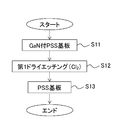
- FIG. 2 is a process diagram showing the flow of a method for manufacturing a recycled substrate in Embodiment 1 of the present invention.
- a thin film of the buffer layer 2 (AlN layer) is formed on the sapphire substrate 1 having a concavo-convex shape (PSS shape 1a) having a triangular surface section.
- the semiconductor substrate 10 on which a thick nitride semiconductor layer 3 (GaN layer) having a flat surface is formed is introduced into a predetermined stage position in a chamber of a substrate processing apparatus for performing dry etching.
- step S12 dry etching is performed by supplying chlorine gas (Cl 2 ) into the chamber of the substrate processing apparatus.
- Cl 2 chlorine gas
- the thin films of the nitride semiconductor layer 3 (GaN layer) and the buffer layer 2 (AlN layer) on the irregular shape of the substrate surface are removed.
- the chlorine gas supplied to the nitride semiconductor layer 3 of the semiconductor substrate 10 is fixed on a stage in a chamber of the substrate processing apparatus with the nitride semiconductor layer 3 facing upward.
- the surface has a triangular cross section as shown in FIG.
- a sapphire substrate 1 having an uneven shape (PSS shape 1a) can be obtained.
- step S13 the nitride semiconductor layer 3 (GaN layer) and the buffer layer 2 (AlN layer) are removed to obtain a sapphire substrate 1 (PSS substrate) having an uneven PSS shape 1a.
- the sapphire substrate 1 (PSS substrate) can be manufactured as a recycled substrate.
- ICP inductively coupled plasma
- FIG. 3 is a main part configuration diagram schematically showing a cross-sectional structure of a substrate processing apparatus used for dry etching in the manufacturing method of the recycled substrate of FIG.
- this substrate processing apparatus 11 is an ICP (inductively coupled plasma) apparatus
- an upper electrode 13 and a lower electrode 14 provided in the processing chamber 12 can be controlled independently.
- a semiconductor substrate 10 that is an insulating substrate can be directly mounted thereon.
- the substrate processing apparatus 11 includes a semiconductor substrate 10 disposed on a stage in a lower electrode 14 in a processing chamber 12 as a processing chamber, and supplies power to the upper electrode 13 and the lower electrode 14 independently, thereby processing chambers.
- a substrate processing apparatus 11 that performs substrate processing (dry etching) by converting chlorine gas (Cl 2 ) or chlorine-based gas (for example, SiCl 4 ) as a processing gas in the plasma into 12 plasma, power is supplied only to the upper electrode 13.
- Substrate processing dry etching
- the substrate processing apparatus 11 controls only the upper electrode 13 while ensuring the back surface He for cooling at a pressure necessary for achieving the process, and the surface area of the insulating substrate on the semiconductor substrate 10 is reduced without using a mechanical chuck.
- a processing gas pressure adjustment process (stability process) in which a processing gas is introduced into the processing chamber 12 instead of an inert gas and the processing gas pressure is adjusted to a predetermined pressure as in the prior art in a state where it is utilized to the maximum by electrostatic adsorption. ),
- the negative charge of the plasma 15 is charged on the semiconductor substrate 10 by the plasma 15 obtained by converting the processing gas into plasma, and the semiconductor substrate 10 is electrostatically adsorbed on the stage of the lower electrode 14 to hold and fix it.
- An adsorption holding process is provided.
- the upper electrode 13 and the lower electrode 14 are both controlled to perform plasma etching.
- the GaN layer as the nitride semiconductor layer 3 and the AlN layer as the buffer layer 2 are removed.
- a plasma 15 of a gas species having a high electron emission rate is generated, and supply of electric charges sufficient to secure adsorption force to the surface of the semiconductor substrate 10 is ensured.
- the ESC voltage to the ESC electrode 16 it is possible to obtain sufficient adsorption force on the surface of the lower electrode 14 of the semiconductor substrate 10 together with the electric charge charged on the surface of the semiconductor substrate 10.
- the application timing of the ESC voltage to the ESC electrode 16 in the adsorption holding process starts at the start of the stability process.
- the semiconductor substrate 10 as an insulating substrate is electrostatically adsorbed by an electrostatic chuck (ESC).
- ESC electrostatic chuck
- the individual RF control of the upper electrode 13 and the lower electrode 14, the adoption of the ESC method, and the selection of conditions (gas type, RFPOWER, application timing, etc.) that make the electron emission rate to the insulator surface of the semiconductor substrate 10 effective are performed.
- a gas species having a high electron emission rate that is easily plasmatized is selected as the processing gas.
- chlorine gas (Cl 2 ) or chlorine-based gas (eg, SiCl 4 ) is used as a gas species having a high electron emission rate.
- the buffer layer 2 (AlN layer) is formed on the sapphire substrate 1, and the nitride semiconductor layer 3 (GaN layer) is formed thereon (or a plurality of layers).
- the semiconductor substrate 10 has a first dry etching step of removing the nitride semiconductor layer 3 (GaN layer) and the buffer layer 2 (AlN layer) therebelow by dry etching.
- the Ga-based nitride semiconductor layer (GaN layer), which has become unusable without obtaining the desired characteristics without adversely affecting the crystallinity and surface irregularity shape, thermally or mechanically as in the past, by the removal method
- the substrate can be regenerated by removing the GaN layer and the AlN layer from the semiconductor substrate 10 as a substrate with a nitride semiconductor layer such as a PSS substrate.
- ICP dry etching is performed by converting chlorine gas (Cl 2 ) under a high flow rate into plasma, and thin films of the nitride semiconductor layer 3 (GaN layer) and the uneven buffer layer 2 (AlN layer) are formed.
- the first dry etching step is not limited to this, and the ICP dry etching is performed by converting chlorine gas (Cl 2 ) under a high flow rate condition into a plasma, and the upper portion of the uneven shape is formed.
- the second dry etching step described in the third embodiment may be performed in which only the nitride semiconductor layer 3 (GaN layer) before or up to the surface of the buffer layer 2 (AlN layer) is removed.
- chlorine gas (Cl 2 ) or a mixed gas of chlorine gas (Cl 2 ) and chlorine-based gas (SiCl 4 ) is used, and in the case of a mixed gas, chlorine gas (Cl 2 )
- a mixed gas chlorine gas (Cl 2 )
- the first dry etching process of the first embodiment includes a second dry etching process in which the nitride semiconductor layer 3 (GaN layer) is removed to the surface of the buffer layer 2 (AlN layer) or a position in the vicinity thereof by dry etching.
- the third dry etching step of removing the remaining nitride semiconductor layer 3 (GaN layer) by dry etching using the buffer layer 2 (AlN layer) as an etch stop layer may be employed. This will be described in detail in the next embodiment liquid 3.
- nitride semiconductor layer 3 or the buffer layer 2 and the nitride semiconductor layer 3 are removed from the semiconductor substrate 10 has been described.
- a plurality of nitride semiconductor layers may be removed by dry etching on a semiconductor substrate having a plurality of nitride semiconductor layers formed on the substrate instead of the semiconductor substrate 10.
- the upper and lower cladding layers and the light emitting layers therebetween are removed from the semiconductor light emitting device formed by sandwiching the light emitting layers between the upper and lower cladding layers as a plurality of nitride semiconductor layers on the semiconductor substrate 10. Thereafter, the buffer layer 2 and the nitride semiconductor layer 3 are further removed from the semiconductor substrate 10.
- Embodiment 2 In the first embodiment, the case where the substrate is regenerated by removing the GaN layer and the AlN layer by performing dry etching has been described. However, in the second embodiment, dry etching and wet etching (AlN residue removal) are performed to further increase the thickness. A case will be described in which the GaN layer and the AlN layer are removed by sonic cleaning (AlN residue removal) and the substrate is regenerated without residue.
- FIG. 4 (a) to 4 (c) are substrate cross-sectional views for explaining a method for manufacturing a recycled substrate according to Embodiment 2 of the present invention.
- FIG. 5 is a process diagram showing a flow of a method for manufacturing a recycled substrate according to Embodiment 2 of the present invention.
- a buffer layer 2 (on the sapphire substrate 1 having a concavo-convex shape (PSS shape 1a) having a triangular surface cross section.
- a predetermined stage position in a chamber of a substrate processing apparatus for performing ICP dry etching on a semiconductor substrate 10 on which a thin nitride semiconductor layer 3 (GaN layer) having a flat surface is formed.
- FIG. 4 (b) and FIG. 5 as shown in, in the first dry etching process at Step S22, chlorine gas (Cl 2 was supplied chlorine gas (Cl 2) into the chamber 12 of the substrate processing apparatus 11 ICP dry etching is performed using plasma.
- the thin films of the nitride semiconductor layer 3 (GaN layer) and the uneven buffer layer 2 (AlN layer) are removed.
- a part of the buffer layer 2 (AlN layer) (residue 2a) remains between the irregular shapes on the surface of the sapphire substrate 1.
- the Al compound generated by dry etching and the buffer layer 2 (AlN layer) partially remained as a residue 2a in the hydrogen peroxide treatment process of Step S23.
- a chemical solution is applied to the sapphire substrate 1 in which the Al compound and the buffer layer 2 (AlN layer) remain as the residue 2a in the sulfuric acid treatment process in step S24.
- the Al compound and the residue 2a of the buffer layer 2 (AlN layer) are removed using a mixed solution of hydrogen peroxide water (H 2 O 2 ) and sulfuric acid (H 2 SO 4 ).
- step S25 the Al compound attached to the sapphire substrate 1 (PSS substrate) and the residue 2a of the buffer layer 2 (AlN layer) are removed by washing with pure water.
- the wet etching process in step S20A is constituted by the hydrogen peroxide solution treatment process in step S23, the sulfuric acid treatment process in step S24, and the water washing process in step S25.
- the sapphire substrate 1 in which the Al compound and the extremely small residue 2a of the buffer layer 2 (AlN layer) remain in the ultrasonic cleaning process in step S26 is used as a chemical solution.
- an ultrasonic cleaning process is performed at an ultrasonic output of 100 W to 500 W used in the ultrasonic vibration device.
- a mixed solution of 2.6 liters of hydrogen peroxide water, 2.6 liters of ammonia water, and 25.8 liters of pure water was used.
- the ratio (volume ratio or weight ratio) of the mixed solution of hydrogen peroxide water, ammonia water and pure water is 1: 1: 1 to 1: 1: 25 (in this case, 1: 1: 10). Used).
- the temperature of the chemical solution used in the ultrasonic cleaning at this time is a temperature range from room temperature RT (for example, 20 degrees Celsius or 25 degrees Celsius) to 45 degrees Celsius.
- step S24 since the sulfuric acid treatment process of step S24 has an adverse effect on the uneven shape of the surface (PSS shape 1a), the next ultrasonic cleaning treatment process is performed even in a state where the treatment time is set as short as possible and a part of the residue 2a is left. Performed to completely remove residue.
- step S27 the sapphire substrate 1 in which the Al compound residue attached to the sapphire substrate 1 (PSS substrate) or the extremely small residue 2a of the buffer layer 2 (AlN layer) remains is washed with pure water to obtain the residue 2a. Remove. In step S28, this is dried.
- the ultrasonic cleaning process of step S26, the water washing process of step S27, and the drying process of step S28 constitute the ultrasonic residue removing process of step S20B.
- the sapphire substrate 1 (PSS substrate with Al residue) in which the Al compound and a partial residue 2 a of the buffer layer 2 (AlN layer) remain between the PSS shapes 1 a.
- the Al compound and the buffer layer 2 (AlN layer) are partially removed (residue 2a) by the wet etching process, and the ultrasonic residue removal process in step S20B completely removes the extremely small residue 2a.
- the sapphire substrate 1 (PSS substrate) having the PSS shape 1a having an uneven surface can be obtained with high quality. In this way, the sapphire substrate 1 (PSS substrate) can be satisfactorily manufactured as a recycled substrate.
- the GaN layer / AlN layer can be completely peeled off with high quality.
- the PSS substrate can be reproduced easily and with high quality without adversely affecting the crystallinity of the sapphire substrate 1 and the uneven shape of the surface.
- FIG. 6 is a main part configuration diagram schematically showing a cross-sectional structure of a substrate processing apparatus used for dry etching with chlorine gas in a high temperature atmosphere without using plasma.
- the substrate processing apparatus 31 includes a processing chamber 32 in which one or a plurality of semiconductor substrates 10 are accommodated, an electric furnace 33 that is disposed above and below the processing chamber 32, and heats the processing chamber 32.
- a stage 34 and a boat 35 for placing one or a plurality of semiconductor substrates 10 in the processing chamber 32 are provided.
- the processing chamber 32 is provided with a gas introduction part 36 for introducing an etching gas such as a chlorine-based gas therein and a gas exhaust part 37 for exhausting an etching gas such as a chlorine-based gas from the inside thereof.
- one or a plurality of semiconductor substrates 10 are disposed in a processing chamber 32, and a dry etching process is performed by introducing a chlorine-based gas into the interior while heating.
- a typical condition is that the heating temperature is 800 degrees Celsius under atmospheric pressure.
- FIG. 7 (a) to 7 (c) are substrate cross-sectional views for explaining a method for manufacturing a recycled substrate according to Embodiment 3 of the present invention.
- FIG. 8 is a process diagram showing the flow of a method for manufacturing a recycled substrate in Embodiment 3 of the present invention.
- a buffer layer 2 (on the sapphire substrate 1 having a surface-repetitive uneven shape (PSS shape 1a) having a triangular cross section).
- a predetermined stage position in a chamber of a substrate processing apparatus for performing ICP dry etching on a semiconductor substrate 10 on which a thin nitride semiconductor layer 3 (GaN layer) having a flat surface is formed.
- the depth of the uneven shape is 0.5 ⁇ m.
- ICP dry etching is performed under a low flow rate condition of SiCl 4 gas with respect to Cl 2 gas. That is, the SiCl 4 gas mixing ratio (volume ratio) to Cl 2 gas is 0.4, and the low selectivity ratio condition (rate ratio is GaN ⁇ AlN ⁇ Al 2 O 3 ), the SiCl gas with respect to the Cl 2 gas flow rate.
- the ICP dry etching is performed by rapidly etching at a high rate with respect to GaN by setting the 4 gas flow rate to a low gas flow rate and increasing the Cl 2 gas flow rate. This ICP dry etching is performed to the surface of the concavo-convex buffer layer 2 (here, the AlN layer), to the front (near the tip), or to the tip.
- the nitride semiconductor layer 3 (GaN layer) on the surface of the concave-convex buffer layer 2 (AlN layer) or in front (near the tip) or up to the tip is removed earlier.
- the mixing ratio of the SiCl 4 gas and the Cl 2 gas is 12:28, and the flow rate of the SiCl 4 gas is not more than half of the Cl 2 gas flow rate (volume ratio).
- ICP dry etching is performed under a high flow rate condition of SiCl 4 gas with respect to Cl 2 gas. That is, ICP dry etching is performed with the SiCl 4 gas flow rate set to a high gas flow rate with respect to the Cl 2 gas flow rate so that the high selection ratio condition (rate ratio is GaN> Al 2 O 3 > AlN).
- SiCl 4 gas since a very low etching rate with respect to the buffer layer 2 (AlN layer) using the same, left the AlN buffer layer 2 as an etch stop layer by increasing the gas flow rate of SiCl 4 gas Only the nitride semiconductor layer 3A (GaN layer) can be removed by etching.
- the semiconductor substrate 10A remaining on the surface of the buffer layer 2 (in this case, the AlN layer) on the uneven shape or in front (near the tip) or up to the tip under a high selection ratio condition of SiCl 4 high flow rate condition,
- the remaining nitride semiconductor layer 3A (GaN layer) is etched away using AlN of the buffer layer 2 as an etch stop layer.
- the mixing ratio of SiCl 4 gas and Cl 2 gas is from 12:28 to 56:28 (“56” is twice that of Cl 2 gas “28”), and the flow rate of SiCl 4 gas is twice that of Cl 2 gas. (Volume ratio).
- the SiCl 4 gas flow rate is increased from less than half (for example, 0.4) to twice the Cl 2 gas flow rate to adjust the high selection ratio condition (rate ratio is GaN> Al 2 O 3 > AlN).
- rate ratio is GaN> Al 2 O 3 > AlN.
- SiCl of more SiCl 4 low flow conditions of the gas was set to the gas flow rate of 0.2-1 times the SiCl 4 gas is Cl 2 gas (volume or weight) (volume), more SiCl 4 gas Four gases are set to a gas flow rate (volume) of 1 to 3 times (volume or weight), more preferably 1.5 to 3 times (easier to determine an etching stop) than Cl 2 gas.
- the buffer layer 2 here, the AlN layer
- etch stop layer etching stop layer
- the depth of the irregularities on the relationship between (0.5 [mu] m), nitrides becomes thin the concentration of Cl 2 gas semiconductor layer 3A Since the etching rate for the (GaN layer) becomes too slow, there is no point in increasing the flow rate ratio of the SiCl 4 gas.
- the flow rate ratio of the SiCl 4 gas to the Cl 2 gas needs to be larger than 3 times (volume mixing ratio).
- the depth (level difference) of the uneven shape on the surface is about 0.3 ⁇ m to 1 ⁇ m.
- the SiCl 4 gas is 1 to 3 times (volume or weight) of the Cl 2 gas, so when the unevenness depth is 1 ⁇ m, the SiCl 4 gas 1-6 times (volume or weight) of Cl 2 gas.
- the SiCl 4 gas is about half of the Cl 2 gas, for example, about 0.4 here, but if the mixing ratio of the SiCl 4 gas to the Cl 2 gas is less than 0.2, the buffer layer 2 (AlN layer) It becomes difficult to control to stop the progress of etching once at the tip of the film.
- the mixture ratio of the SiCl 4 gas may be 0 for dry etching the nitride semiconductor layer 3 (GaN layer).
- the low-flow conditions SiCl 4 gas, SiCl 4 gas mixture ratio and Cl 2 gas are set to 12:28, high flow conditions SiCl 4 gas, SiCl 4 gas and Cl 2
- the gas mixing ratio is set to 56:28.
- the nitride semiconductor layer 3 (GaN layer) is sequentially removed by mixing Cl 2 gas and SiCl 4 gas, and the surface of the buffer layer 2 (AlN layer) near the uneven surface or in front thereof.
- the ratio of the SiCl 4 gas flow rate to the Cl 2 gas flow rate is increased to remove only the nitride semiconductor layer 3A (GaN layer) using the buffer layer 2 as an etch stop layer.
- the sapphire substrate 1 (PSN substrate with AlN) in which the thin film of the buffer layer 2 (AlN layer) remains on the PSS shape 1a without the residue of the GaN layer can be obtained.
- the sapphire substrate 1 (PSN substrate with AlN) in which the thin film of the buffer layer 2 (AlN layer) remains can be manufactured as a reproduction substrate.
- ICP dry etching is performed by mixing Cl 2 gas and SiCl 4 gas, and after the etching proceeds to the surface of the buffer layer 2 (AlN layer) on the uneven surface or the vicinity thereof, A chemical and simple removal method of adjusting the flow rate ratio of the SiCl 4 gas to remove the nitride semiconductor layer 3 (GaN film) using the buffer layer 2 (AlN layer) as an etch stop layer.
- the PSS substrate with AlN can be reproduced with high quality without adversely affecting the crystallinity and uneven shape of the sapphire substrate 1.
- the buffer layer 2 (AlN layer) on the uneven surface can be used as it is, the step of forming the buffer layer 2 (AlN layer) can be omitted. Further, in the third embodiment, since there is no wet etching processing step in step S20A and the ultrasonic residue removing step in step S20B in the second embodiment, a recycled substrate can be manufactured with a smaller number of steps.
- FIG. 9 (a) to 9 (d) are substrate cross-sectional views for explaining a method for manufacturing a recycled substrate in Embodiment 4 of the present invention.
- FIG. 10 is a process diagram showing a flow of a method for manufacturing a recycled substrate in Embodiment 4 of the present invention.
- a buffer layer 2 on the sapphire substrate 1 having a concavo-convex shape (PSS shape 1a) having a triangular surface cross section.
- a predetermined stage position in a chamber of a substrate processing apparatus for performing ICP dry etching on a semiconductor substrate 10 on which a thin nitride semiconductor layer 3 (GaN layer) having a flat surface is formed.
- step S42 the Cl 2 gas into the chamber of the substrate processing apparatus at a high flow rate conditions of Cl 2 gas (chlorine gas)
- the Cl 2 gas (chlorine gas) is turned into plasma, and the semiconductor substrate 10 is ICP dry etched to further form the nitride semiconductor layer 3 (GaN layer) before the buffer layer 2 (AlN layer) above the uneven shape. Remove quickly.
- the Cl 2 gas flow rate is set so that the high selection ratio condition (rate ratio is GaN> Al 2 O 3 > AlN).
- ICP dry etching is performed with the SiCl 4 gas flow rate set to a high gas flow rate.
- the semiconductor substrate 10A remaining on the surface of the buffer layer 2 (in this case, the AlN layer) above the uneven shape or in front (near the tip) or up to the tip under a high selection ratio condition of SiCl 4 high flow rate condition,
- a high selection ratio condition of SiCl 4 high flow rate condition By ICP dry etching, AlN of the buffer layer 2 is used as an etch stop layer (etching stop layer), and the remaining GaN layer of the nitride semiconductor layer 3A is etched away.
- the mixing ratio of SiCl 4 gas and Cl 2 gas is set to about 56:28.
- the SiCl 4 gas flow rate is increased from 1.5 times to 3 times (here, 2 times) with respect to the Cl 2 gas flow rate so that a high selection ratio condition (rate ratio is GaN> Al 2 O 3 > AlN)
- rate ratio is GaN> Al 2 O 3 > AlN
- dry etching removes the nitride semiconductor layer 3 (GaN layer) halfway with chlorine gas (Cl 2 gas) and chlorine-based gas (SiCl 4 gas), and the buffer layer 2 (AlN layer) near the uneven surface.
- the mixing ratio of the SiCl 4 gas to the Cl 2 gas is increased, and the nitride semiconductor layer 3A remaining with the buffer layer 2 as an etch stop layer Just get rid of.
- the sapphire substrate 1 PSN substrate with AlN
- the thin film of the buffer layer 2 (AlN layer) remains on the PSS shape 1a can be obtained.
- step S44 a mixed solution of hydrogen peroxide (H 2 O 2 ) and sulfuric acid (H 2 SO 4 ) is used as the chemical.
- the buffer layer 2 AlN layer is removed by wet etching.
- step S45 the residue of the buffer layer 2 (AlN layer) attached to the sapphire substrate 1 (PSS substrate) is removed by washing with pure water.
- step S46 this is dried.
- the wet etching process in step S40 is constituted by the chemical solution process in step S44, the water washing process in step S45, and the drying process in step S46.
- the sapphire substrate 1 (PSN substrate with AlN) in which the thin film of the buffer layer 2 (AlN layer) remains on the PSS shape 1a is formed.
- the buffer layer 2 (AlN layer) is removed by the wet etching process in step S40, and the sapphire substrate 1 (PSS substrate) having the PSS shape 1a having an uneven surface can be obtained in step S47. In this way, the sapphire substrate 1 (PSS substrate) can be manufactured as a recycled substrate.
- the PSS substrate can be reproduced with high quality without adversely affecting the crystallinity and uneven shape of the sapphire substrate by a simple chemical removal method.
- FIG. 11 is a block diagram for explaining the relationship between the manufacturing methods of the respective reproduction substrates of the first to fourth embodiments.
- step S51 ICP dry etching is performed with chlorine gas (Cl 2 ) under a high flow rate condition, so that the nitride semiconductor layer 3 (GaN layer) and the uneven buffer layer 2 (AlN Layer) is removed together.
- Cl 2 chlorine gas
- step S51 chlorine gas (Cl 2 ) under a high flow rate condition is converted into plasma and ICP dry etching is performed, so that the nitride semiconductor layer 3 (GaN) before the buffer layer 2 (AlN layer) above the uneven shape is formed. Only the layer) is removed.
- This is the second dry etching step of the third embodiment.
- step S52 ICP dry etching is performed by converting chlorine gas (Cl 2 ) under a low flow rate into plasma, and the GaN layer of the nitride semiconductor layer 3 is etched using AlN of the buffer layer 2 as an etch stop layer. Remove.
- This is the third dry etching step of the third embodiment.
- the PSS shape 1a is better than that after the first dry etching process of the first embodiment.
- step S53 a wet etching process including sulfuric acid treatment is performed, and in step S54, an ultrasonic residue removing process including ultrasonic cleaning is performed to remove the GaN layer and the AlN layer, and to remove the AlN layer residue. Perform substrate regeneration.
- This is the wet etching process and the ultrasonic residue removing process of the second embodiment. Therefore, in the second embodiment, the wet etching process and the ultrasonic residue removing process are sequentially performed after the first dry etching process of the first embodiment.
- step S53 sulfuric acid treatment is further performed in step S53.
- the PSS substrate is regenerated by removing the buffer layer 2 (AlN layer) by performing a wet etching process including Thereafter, an ultrasonic residue removing process including an ultrasonic cleaning process in step S54 may be performed to more reliably remove residues on the surface.
- the PSS substrate with AlN regenerated by removing the nitride semiconductor layer 3 (GaN layer), or the PSS substrate from which the nitride semiconductor layer 3 (GaN layer) and the buffer layer 2 (AlN layer) are removed.
- a semiconductor light emitting element is formed, in which a light emitting layer is sandwiched between upper and lower cladding layers. This will be described with reference to FIG.
- FIG. 12 is a longitudinal sectional view showing an example of the configuration of the main part of a nitride semiconductor light emitting device using a reproduction substrate manufactured by the method for manufacturing each reproduction substrate according to Embodiments 1 to 4 of the present invention.
- the nitride semiconductor light emitting device 20 using each reproduction substrate of Embodiments 1 to 4 is, for example, on the sapphire substrate 1 as a substrate having an uneven shape (PSS shape 1a) and a thickness of about 1300 ⁇ m. Further, a buffer layer 2 made of aluminum nitride (AlN) having a thickness of about 50 nm is formed, and a nitride semiconductor layer 3 which is a non-doped GaN layer having a thickness of about 10 ⁇ m made of non-doped GaN is formed thereon. Yes.
- the sapphire substrate 1, the buffer layer 2, and the nitride semiconductor layer 3 (GaN layer) constitute a semiconductor substrate 10 that is a single crystal substrate.
- the nitride semiconductor layer 3 (GaN layer) of the nitride semiconductor layer 3 (GaN layer) and the buffer layer 2 (AlN layer) is removed from the unusable semiconductor substrate 10 in the above embodiment.
- the reproduction substrate (PSS substrate or PSS substrate with AlN) obtained in 1 to 4 is used, and the buffer layer 2 (AlN layer) and the nitride semiconductor layer 3 (GaN layer) or the nitride semiconductor layer 3 are again formed on the reproduction substrate. (GaN layer) is replaced and reproduced.
- an n-type contact layer 41 (about 5 ⁇ m thick) made of GaN doped with silicon (Si) 1 ⁇ 10 18 / cm 3 on the semiconductor substrate 10 of the single crystal substrate.
- a high carrier concentration n ⁇ + layer is formed.
- a multi-layer 51 is formed on the n-type contact layer 41, and a light-emitting layer 52 having a multi-quantum well structure is formed on the multi-layer 51.
- an electron block layer 6 which is a p-type layer made of 25 nm-thick p-type Al — 0.15 Ga — 0.85 N doped with 2 ⁇ 10 19 / cm 3 of Mg, is formed on the light emitting layer 52.
- a p-type contact layer 42 made of 100-nm thick p-type GaN doped with 8 ⁇ 10 19 Mg is formed.
- a light-transmitting thin film electrode 7 (ITO) is formed by metal deposition, and a p-electrode 81 is formed on a part of the light-transmitting thin film electrode 7, while the n-type contact layer
- An n electrode 82 is formed on the end of 41.
- a protective film 9 made of a SiO 2 film is formed on the top.
- the case where the sapphire substrate 1 having a concavo-convex shape (PSS shape 1a) is used has been described.
- the present invention is not limited thereto, and the concavo-convex processing is performed on the surface of the substrate such as the sapphire substrate 1.
- the inventions of Embodiments 1 to 4 can also be applied when no is applied.
- the present invention relates to a method of manufacturing a regenerated substrate in which a regenerated substrate is manufactured by removing the laminated semiconductor layer from the laminated semiconductor wafer in order to reuse the substrate for the laminated semiconductor wafer on which the laminated semiconductor layer is formed.
- the PSS substrate with a GaN layer that has become unusable can be regenerated with high quality without adversely affecting the crystallinity of the substrate and the surface irregularities.
Landscapes
- Led Devices (AREA)
- Drying Of Semiconductors (AREA)
Abstract
簡便な方法で、基板の結晶性や表面凹凸形状に悪影響を与えずに、使用不可能になったGaN層付きPSS基板を品質良く再生する。 サファイヤ基板1上にバッファ層2(AlN層)窒化物半導体層3(GaN層)が1層(または複数層)形成された半導体基板10に対してドライエッチングにより前記窒化物半導体層3(GaN層)および前記バッファ層2(AlN層)を除去する第1ドライエッチング工程を有している。
Description
本発明は、半導体層を順次成膜して積層された半導体ウエハに対して、その基板を再び利用するために、半導体ウエハから使用不可能になった半導体層を除去して再生基板を製造する再生基板の製造方法に関する。
この種の従来の再生基板の製造方法は、加熱処理により半導体ウエハから半導体層を昇華させて取り除く特許文献1および、ブラスト材を噴射して半導体ウエハから半導体層を機械的に削って除去する特許文献2に提案されている。
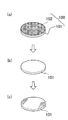
図13(a)~図13(c)は、特許文献1に開示されている従来の再生基板の製造方法の一例を示す模式図である。
まず、図13(a)に示すように、再生処理の対象となる半導体ウエハ100は、基板101と、基板101上に成膜された半導体層102とを備えている。
半導体ウエハ100を構成する基板101としてはサファイア基板を用いる。また、半導体層102としては、III-V族化合物半導体層、中でもIII族窒化化合物半導体層が好ましい。例えば、InGaN、AlGaNまたはGaNからなるバッファ層を基板101上に備えている。この場合の半導体ウエハ100は、例えば青色光を出力する青色発光チップさらには青色発光チップを用いた発光装置を製造するための出発材料になっている。
次に、図13(b)に示すように、除去工程では、半導体ウエハ100に対して加熱処理を施すことにより半導体層102の除去を行う。この加熱処理は半導体層102の昇華点以上でかつ基板101の融点より低い温度に半導体ウエハ100を加熱する。
この除去工程は、半導体ウエハ100を加熱装置のチャンバ内に設置するウエハ設置工程と、加熱装置のチャンバ内を減圧する減圧工程と、半導体ウエハ100の温度を上昇させる昇温工程と、半導体ウエハ100を所定の温度に一定の時間保持する温度保持工程と、半導体ウエハ100から半導体層102が熱により除去されて残った基板101の温度を下げる降温工程とを有している。
その後、図13(c)に示すように、洗浄工程では、除去工程によって半導体層102が除去された基板101に対して洗浄剤を用いた洗浄を行う。
このように、以上の従来の再生基板の製造方法では、半導体層102を取り除く除去工程としての加熱工程と、半導体層102を取り除いた基板101の表面を洗浄する洗浄工程とを有している。
このようにして、半導体ウエハ100から、使用不可能になった半導体層102を取り除いて、基板101を再び利用可能に再生することができる。
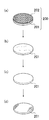
図14(a)~図14(d)は、特許文献2に開示されている従来の再生基板の製造方法の一例を示す模式図である。
まず、図14(a)に示すように、基板再生処理の対象となる半導体ウエハ200は、サファイア基板などの基板201と、この基板201上に成膜された半導体層202とを備えている。半導体層202は、例えばInGaN、AlGaNまたはGaNからなるバッファ層を初めとするIII族窒化物化合物半導体層である。
次に、図14(b)に示すように、ブラスト処理工程では、処理対象となる半導体ウエハ200に対してブラスト材を噴射して半導体ウエハ200から半導体層202を除去する。
ブラスト処理工程ではブラスト装置を用いる。ブラスト装置は、半導体ウエハ200を搬送する搬送部と、半導体ウエハ200の半導体層202側に向けて、ブラスト材を水に混合したスラリをノズルから噴射するブラスト処理部と、噴射後のスラリなどを回収する回収部と、ブラスト装置全体を統括的に制御する制御部とを備えている。
このブラスト材としては、III族窒化物化合物(例えばGaN)よりも硬く、サファイア基板以下の硬さを持つものを用いる。具体的には、サファイア基板を構成する物質である酸化アルミニウムの粒(アルミナ粒)をブラスト材に用いている。これは、ブラスト処理工程の後にサファイア基板にアルミナ粒の一部が残ったとしても、サファイア基板とアルミナ粒とが同種であるため、再生後の基板101に残存するブラスト材がその後の工程に及ぼす影響を極めて小さくするためである。
その後、図14(c)に示すように、熱処理工程では、半導体層202が除去された基板201を所定温度(例えば摂氏1400度)に加熱する。半導体層202が取り除かれた基板201に対して熱処理を施すことにより、基板201における結晶歪みの除去を図っている。
続いて、図14(d)に示すように、研磨工程では、熱処理が施された基板201に対して基板201の表面を研磨する。この研磨工程では、基板201を載せる定盤と、基板201の表面を研磨する研磨パッドとを有する研磨装置を用いる。
このように、再生基板の製造方法では、ブラスト処理工程と、熱処理工程と、研磨加工工程とを有している。
特許文献1に開示されている上記従来の再生基板の製造方法では、加熱処理により半導体ウエハ100の基板101上から半導体層102を昇華させて熱的に取り除いており、特許文献2に開示されている上記従来の再生基板の製造方法では、ブラスト材を噴射させて半導体ウエハ200の基板201上から半導体層202を機械的に削って除去している。
ところが、特許文献1、2のように、熱的、機械的に半導体層として窒化物半導体層の剥離を行うと、基板の結晶性に悪影響を与えたり、基板表面の凹凸形状に悪影響を与える虞がある。特に、サファイヤ基板の表面に凹凸構造の断面三角形のPSS形状を正確に維持して基板を再生する必要がある。
本発明は、上記従来の問題を解決するもので、簡便な方法で、基板の結晶性や表面凹凸形状に悪影響を与えずに、使用不可能になった窒化物半導体層付き基板を品質良く再生することができる再生基板の製造方法を提供することを目的とする。
本発明の再生基板の製造方法は、基板上に窒化物半導体層が一または複数層形成された半導体基板に対してドライエッチングにより少なくとも該窒化物半導体層を除去する第1ドライエッチング工程を有するものであり、そのことにより上記目的が達成される。
また、好ましくは、本発明の再生基板の製造方法において、前記基板と前記窒化物半導体層の間にバッファ層が設けられており、該窒化物半導体層および該バッファ層を除去する前記ドライエッチングにより残った残渣を除去するウエットエッチング工程をさらに有する。
さらに、好ましくは、本発明の再生基板の製造方法におけるウエットエッチング工程で過酸化水素水と硫酸の混合液を用い、前記バッファ層はAlN層であり、前記残渣としてAl化合物および該AlN層の残渣をさらに除去する超音波残渣除去工程を有し、該超音波残渣除去工程で用いる薬液は、過酸化水素水とアンモニア水の混合液であるかまたは、過酸化水素水、アンモニア水および純水の混合液である。
さらに、好ましくは、本発明の再生基板の製造方法において、前記基板と前記窒化物半導体層の間にバッファ層が設けられ、前記第1ドライエッチング工程は、ドライエッチングにより該バッファ層の表面またはその近傍位置まで該窒化物半導体層を除去する第2ドライエッチング工程と、該バッファ層をエッチストップ層としてドライエッチングにより残りの該窒化物半導体層を除去する第3ドライエッチング工程とを有する。
さらに、好ましくは、本発明の再生基板の製造方法における第2ドライエッチング工程としてCl2ガスとSiCl4 ガスの混合ガスを用いて前記バッファ層の表面またはその近傍位置までエッチング進行後、前記第3ドライエッチング工程として該Cl2ガスに対するSiCl4 ガスの流量比を増加させるようにガス流量を調整する。
また、好ましくは、本発明の再生基板の製造方法における半導体基板の基板表面には凹凸加工が施されている。
さらに、好ましくは、本発明の再生基板の製造方法におけるドライエッチングには塩素ガスおよび塩素系ガスの少なくともいずれかを用いる。
さらに、好ましくは、本発明の再生基板の製造方法における基板と前記窒化物半導体層の間にAlNバッファ層が設けられており、過酸化水素水と硫酸の混合液を用いたウエットエッチングにより前記ドライエッチング工程で除去した後のAl化合物およびAlNバッファ層の残渣を除去するウエットエッチング工程を有する。
さらに、好ましくは、本発明の再生基板の製造方法におけるウエットエッチング工程で除去した後のAl化合物およびAlNバッファ層の残渣をさらに除去する超音波残渣除去工程を有し、該超音波残渣除去工程で用いる薬液は、過酸化水素水とアンモニア水の混合液であるかまたは、過酸化水素水、アンモニア水および純水の混合液である。
さらに、好ましくは、本発明の再生基板の製造方法における過酸化水素水、アンモニア水および純水の混合液の混合比は、1:1:1から1:1:25の範囲内である。
さらに、好ましくは、本発明の再生基板の製造方法における超音波残渣除去工程での超音波出力は100Wから500Wの範囲内である。
さらに、好ましくは、本発明の再生基板の製造方法における薬液温度は、摂氏20度から摂氏45度である。
本発明の再生基板の製造方法は、基板上にバッファ層とその上層に窒化物半導体層が形成された半導体基板に対してドライエッチングにより該バッファ層またはその近傍位置まで該窒化物半導体層を除去する第2ドライエッチング工程と、該バッファ層をエッチストップ層としてドライエッチングにより該窒化物半導体層を除去する第3ドライエッチングとを有するものであり、そのことにより上記目的が達成される。
また、好ましくは、本発明の再生基板の製造方法における半導体基板の基板表面には凹凸加工が施されている。
さらに、好ましくは、本発明の再生基板の製造方法における第2ドライエッチング工程としてCl2ガスとSiCl4 ガスの混合ガスを用いて前記バッファ層の凹凸表面またはその近傍位置までエッチング進行後、前記第3ドライエッチング工程として該Cl2ガスに対するSiCl4 ガスの流量比を増加させるようにガス流量を調整する。
さらに、好ましくは、本発明の再生基板の製造方法における第3ドライエッチング工程により前記窒化物半導体層を取り除いた後に、薬液によりバッファ層を除去するバッファ層除去工程を有する。
さらに、好ましくは、本発明の再生基板の製造方法におけるバッファ層はAlN層である。
さらに、好ましくは、本発明の再生基板の製造方法における薬液は硫酸と過酸化水素水の混合液である。
上記構成により、以下、本発明の作用を説明する。
本発明においては、基板上に窒化物半導体層が一または複数層形成された半導体基板に対してドライエッチングにより少なくとも窒化物半導体層を除去する第1ドライエッチング工程を有している。
これによって、ドライエッチングによる簡便な化学的な方法により、従来のように基板の結晶性や表面凹凸形状に悪影響を与えずに、不純物混入などで使用不可能になったGaN層付きPSS基板などの窒化物半導体層付き基板を品質良く再生することが可能となる。
以上により、本発明によれば、ドライエッチングによる簡便な化学的な方法により、従来のように基板の結晶性や表面凹凸形状に悪影響を与えずに、使用不可能になったGaN層付きPSS基板などの窒化物半導体層付き基板を品質良く再生することができる。
[規則91に基づく訂正 02.07.2014]
(a)および(b)は、本発明の実施形態1における再生基板の製造方法を説明するための基板断面図である。
本発明の実施形態1における再生基板の製造方法の流れを示す工程図である。
図1の再生基板の製造方法のICPドライエッチングに用いる基板処理装置の断面構造を模式的に示す要部構成図である。
(a)~(c)は、本発明の実施形態2における再生基板の製造方法を説明するための基板断面図である。
本発明の実施形態2における再生基板の製造方法の流れを示す工程図である。
プラズマを用いない、高温雰囲気下での塩素ガスによるドライエッチングに用いる基板処理装置の断面構造を模式的に示す要部構成図である。
(a)~(c)は、本発明の実施形態3における再生基板の製造方法を説明するための基板断面図である。
本発明の実施形態3における再生基板の製造方法の流れを示す工程図である。
(a)~(d)は、本発明の実施形態4における再生基板の製造方法を説明するための基板断面図である。
本発明の実施形態4における再生基板の製造方法の流れを示す工程図である。
上記実施形態1~4の各再生基板の製造方法の関係について説明するためのブロック図である。
本発明の実施形態1~4の各再生基板の製造方法により製造された再生基板を用いた窒化物半導体発光素子の要部構成例を示す縦断面図である。
(a)~(c)は、特許文献1に開示されている従来の再生基板の製造方法の一例を示す模式図である。
(a)~(d)は、特許文献2に開示されている従来の再生基板の製造方法の一例を示す模式図である。
1 サファイヤ基板
1a PSS形状(凹凸形状)
2 バッファ層(AlN層)
2a バッファ層(AlN層)やAl化合物の残渣
3、3A 窒化物半導体層(GaN層)
41 n型コンタクト層
42 p型コンタクト層
51 多重層
52 発光層
6 電子ブロック層
7 透光性薄膜電極
81 p電極
82 n電極
9 保護膜
10、10A 半導体基板(単結晶性基板)
11 基板処理装置
12 処理チャンバ
13 上部電極
14 下部電極
15 プラズマ
16 ESC電極
20 窒化物半導体発光素子
31 基板処理装置
32 処理チャンバ
33 電気炉
34 ステージ
35 ボート
36 ガス導入部
37 ガス排気部
1a PSS形状(凹凸形状)
2 バッファ層(AlN層)
2a バッファ層(AlN層)やAl化合物の残渣
3、3A 窒化物半導体層(GaN層)
41 n型コンタクト層
42 p型コンタクト層
51 多重層
52 発光層
6 電子ブロック層
7 透光性薄膜電極
81 p電極
82 n電極
9 保護膜
10、10A 半導体基板(単結晶性基板)
11 基板処理装置
12 処理チャンバ
13 上部電極
14 下部電極
15 プラズマ
16 ESC電極
20 窒化物半導体発光素子
31 基板処理装置
32 処理チャンバ
33 電気炉
34 ステージ
35 ボート
36 ガス導入部
37 ガス排気部
以下に、本発明の再生基板の製造方法の実施形態1~4について図面を参照しながら詳細に説明する。なお、各図における構成部材のそれぞれの厚みや長さなどは図面作成上の観点から、図示する構成に限定されるものではない。また、繰り返し断面三角形の凹凸形状の個数も実際のデバイスと一致していなくてもよく、図示および説明の便宜を考慮した個数としたものであり、図示する構成に限定されるものではない。
(実施形態1)
本実施形態1では、ドライエッチング(GaN除去またはAlN+GaN除去)について説明する。
本実施形態1では、ドライエッチング(GaN除去またはAlN+GaN除去)について説明する。
図1(a)および図1(b)は、本発明の実施形態1における再生基板の製造方法を説明するための基板断面図である。
図1(a)および図1(b)において、本実施形態1の再生基板の製造方法は、サファイヤ基板1の凹凸上に薄いバッファ層2とその上層に窒化物半導体層3が形成された半導体基板10をドライエッチングすることにより半導体基板10から窒化物半導体層3または、バッファ層2および窒化物半導体層3を取り除いて再生基板とする第1ドライエッチング工程を有している。
この半導体基板10において、表面に繰り返し断面三角形状の凹凸構造が形成された厚さ例えば約1300μmの基板としての例えばサファイヤ基板1上に、窒化アルミニウム(AlN)から成る膜厚が例えば約50nmの薄いバッファ層2が成膜されている。バッファ層2の表面は、サファイヤ基板1上の凹凸形状が反映された凹凸形状になっている。その上に窒化物半導体層3としてノンドープのGaNから成る膜厚が例えば約10μmのノンドープGaN層が成膜されている。窒化物半導体層3(GaN層)の表面は平坦になっている。これらのサファイヤ基板1、その上のAlN層のバッファ層2およびその上のノンドープGaN層などの窒化物半導体層3が単結晶性基板(GaN層付きPSS基板)を構成している。この単結晶性基板(GaN層付きPSS基板)を用いてその上に上下のクラッド層間に発光層が挟まれて半導体発光素子が形成される。
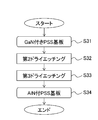
図2は、本発明の実施形態1における再生基板の製造方法の流れを示す工程図である。
図2に示すように、ステップS11のGaN付きPSS基板受け入れ工程において、表面繰り返し断面三角形状の凹凸形状(PSS形状1a)を持つサファイヤ基板1上にバッファ層2(AlN層)の薄膜が形成され、その上層に表面が平坦な厚い窒化物半導体層3(GaN層)が形成された半導体基板10を、ドライエッチングを行う基板処理装置のチャンバ内の所定ステージ位置に導入する。
次に、ステップS12の第1ドライエッチング工程において、基板処理装置のチャンバ内に塩素ガス(Cl2)を供給してドライエッチングを行う。これによって、窒化物半導体層3(GaN層)および基板表面の凹凸形状上のバッファ層2(AlN層)の薄膜を除去する。
第1ドライエッチング工程(窒化物半導体層除去工程)では、半導体基板10の窒化物半導体層3を上にして、基板処理装置のチャンバ内のステージ上に固定して、その上方に供給した塩素ガス(Cl2)によってドライエッチングを行ってGaN層の窒化物半導体層3さらに薄いAlN層からなるバッファ層2を共に除去することにより、図1(b)に示すように表面の繰り返し断面三角形状の凹凸形状(PSS形状1a)を持つサファイヤ基板1を得ることができる。
このように、ステップS13で窒化物半導体層3(GaN層)さらにバッファ層2(AlN層)を取り除いて表面が凹凸形状のPSS形状1aを持つサファイヤ基板1(PSS基板)を得ることができる。このようにして、サファイヤ基板1(PSS基板)を再生基板として製造することができる。
ここで、図1の再生基板の製造方法のドライエッチングに用いる基板処理装置としてのICP(誘導結合プラズマ)装置について説明する。
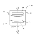
図3は、図1の再生基板の製造方法のドライエッチングに用いる基板処理装置の断面構造を模式的に示す要部構成図である。
図3において、この基板処理装置11は、ICP(誘導結合プラズマ)装置であることから処理チャンバ12内に設けられた上部電極13と下部電極14とが独立して制御可能であり、下部電極14上に絶縁基板である半導体基板10を直に搭載可能である。
この基板処理装置11は、処理室としての処理チャンバ12内の下部電極14におけるステージ上に半導体基板10を配置し、上部電極13と下部電極14それぞれに独立して電力を供給して、処理チャンバ12内の処理ガスとしての塩素ガス(Cl2)や塩素系ガス(例えばSiCl4)をプラズマ化して基板処理(ドライエッチング)を行う基板処理装置11において、上部電極13のみに電力を供給して、不活性ガスに比べてプラズマ化し易い電子放出率の高い、処理チャンバ12内に供給した処理ガスとしての塩素ガス(Cl2)や塩素系ガス(例えばSiCl4)をプラズマ化して半導体基板10に電荷を帯電させて下部電極14側に半導体基板10を静電吸着させた基板固定状態で基板処理(ドライエッチング)が実施可能となる。
この基板処理装置11は、プロセス達成に必要な圧力の冷却用の裏面Heを確保しながら、上部電極13だけを制御して、絶縁基板の半導体基板10上の表面積を、メカニカルチャックを用いず、静電吸着により最大限に活用した状態で、従来のように不活性ガスではなく処理ガスを処理チャンバ12内に導入して処理ガス圧力を所定圧力に調整する処理ガス圧力調整工程(スタビリティ工程)内で、処理ガスをプラズマ化したプラズマ15により、半導体基板10上にプラズマ15の陰電荷を帯電させて、下部電極14のステージ上に半導体基板10を静電吸着してこれを保持固定する吸着保持工程を設けている。
その後、上部電極13と下部電極14とが共に制御されてプラズマエッチングが実施される。このプラズマエッチングによって、窒化物半導体層3としてのGaN層およびバッファ層2としてのAlN層を除去する。
この吸着保持工程において、処理ガスとして電子放出率の高いガス種の塩素ガス(Cl2)や塩素系ガス(例えばSiCl4)を選択する。上部電極13のみのRF印加により、その電子放出率の高いガス種のプラズマ15を生成し、半導体基板10の表面への吸着力確保に十分な電荷の供給を確保する。ESC電極16へのESC電圧の印加により、半導体基板10の表面に帯電された電荷と合わせて十分な半導体基板10の下部電極14の表面への吸着力を得ることができる。吸着保持工程のESC電極16へのESC電圧の印加タイミングは、スタビリティ工程の開始時に開始する。基板吸着工程は、絶縁基板の半導体基板10を、静電チャック(ESC)により静電吸着させる。
上部電極13と下部電極14のRF個別制御、ESC方式の採用および半導体基板10の絶縁体表面への電子放出率が効果的になる条件(ガス種、RFPOWER、印加タイミングなど)の選択を行う。要するに、処理ガスとしてプラズマ化し易い電子放出率の高いガス種を選択する。ここでは、電子放出率の高いガス種として例えば塩素ガス(Cl2)や塩素系ガス(例えばSiCl4)を用いる。
以上により、本実施形態1によれば、サファイヤ基板1上にバッファ層2(AlN層)が形成され、その上に窒化物半導体層3(GaN層)が1層(または複数層)形成された半導体基板10に対して、ドライエッチングにより、窒化物半導体層3(GaN層)およびその下のバッファ層2(AlN層)を除去する第1ドライエッチング工程を有している。
これによって、プラズマエッチングによって、窒化物半導体層3としてのGaN層およびバッファ層2としてのAlN層を除去する熱的な除去方法や機械的な除去方法を用いないドライエッチングだけの化学的な簡便な除去方法により、従来のように熱的または機械的に結晶性や表面凹凸形状に悪影響を与えることなく、所望の特性が得られず使用不可能になっていたGa系窒化物半導体層(GaN層を含む)付きPSS基板などの窒化物半導体層付き基板としての半導体基板10からGaN層およびAlN層を除去して基板再生を可能とする。
本実施形態1では、高流量条件の塩素ガス(Cl2)をプラズマ化してICPドライエッチングを行い、窒化物半導体層3(GaN層)および凹凸形状上のバッファ層2(AlN層)の薄膜を共に除去する第1ドライエッチング工程として説明したが、これに限らず、第1ドライエッチング工程は、高流量条件の塩素ガス(Cl2)をプラズマ化してICPドライエッチングを行って、凹凸形状の上方のバッファ層2(AlN層)の手前または表面までの窒化物半導体層3(GaN層)だけを除去する実施形態3で説明する第2ドライエッチング工程としてもよい。
本実施形態1の第1ドライエッチング工程において、塩素ガス(Cl2)または、塩素ガス(Cl2)と塩素系ガス(SiCl4)の混合ガスを用い、混合ガスの場合は、塩素ガス(Cl2)に対する塩素系ガス(SiCl4)の混合比は半分以下とする。これは後述する実施形態3の第2ドライエッチング工程に対応している。
この場合、本実施形態1の第1ドライエッチング工程は、ドライエッチングによりバッファ層2(AlN層)の表面またはその近傍位置まで窒化物半導体層3(GaN層)を除去する第2ドライエッチング工程と、バッファ層2(AlN層)をエッチストップ層としてドライエッチングにより残りの窒化物半導体層3(GaN層)を除去する第3ドライエッチング工程とを有するように構成することもできる。これは次の実施液体3で詳細に説明する。
なお、本実施形態1では、説明を簡略化するために、半導体基板10から窒化物半導体層3または、バッファ層2および窒化物半導体層3を取り除く場合について説明したが、これに限らず、第1ドライエッチング工程として、半導体基板10の代わりに、基板上に窒化物半導体層が複数層形成された半導体基板に対してドライエッチングにより複数の窒化物半導体層を除去する場合もある。
これは、例えば、半導体基板10上に、複数の窒化物半導体層として上下のクラッド層およびその間に発光層が挟まれて形成された半導体発光素子から、上下のクラッド層およびその間の発光層を取り除いた後に、半導体基板10からさらにバッファ層2および窒化物半導体層3を取り除く場合などである。
(実施形態2)
上記実施形態1では、ドライエッチングを行ってGaN層およびAlN層を除去して基板再生を行う場合について説明したが、本実施形態2では、ドライエッチングおよびウエットエッチング(AlN残渣除去)を行いさらに超音波洗浄(AlN残渣除去)を行ってGaN層およびAlN層を除去して残渣なく基板再生を行う場合について説明する。
上記実施形態1では、ドライエッチングを行ってGaN層およびAlN層を除去して基板再生を行う場合について説明したが、本実施形態2では、ドライエッチングおよびウエットエッチング(AlN残渣除去)を行いさらに超音波洗浄(AlN残渣除去)を行ってGaN層およびAlN層を除去して残渣なく基板再生を行う場合について説明する。
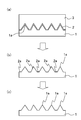
図4(a)~図4(c)は、本発明の実施形態2における再生基板の製造方法を説明するため基板断面図である。図5は、本発明の実施形態2における再生基板の製造方法の流れを示す工程図である。
まず、図4(a)および図5に示すように、ステップS21のGaN付きPSS基板受け入れ工程において、表面繰り返し断面三角形状の凹凸形状(PSS形状1a)を持つサファイヤ基板1上にバッファ層2(AlN層)の薄膜が形成され、その上層に表面が平坦な厚い窒化物半導体層3(GaN層)が形成された半導体基板10を、ICPドライエッチングを行う基板処理装置のチャンバ内の所定ステージ位置に導入する。
次に、図4(b)および図5に示すように、ステップS22の第1ドライエッチング工程において、基板処理装置11のチャンバ12内に塩素ガス(Cl2)を供給して塩素ガス(Cl2)をプラズマ化してICPドライエッチングを行う。
これによって、窒化物半導体層3(GaN層)および凹凸形状上のバッファ層2(AlN層)の薄膜を除去する。このとき、サファイヤ基板1の表面の凹凸形状間にバッファ層2(AlN層)が一部(残渣2a)残ってしまう。
その後、図4(c)および図5に示すように、ステップS23の過酸化水素水処理工程により、ドライエッチングで生成されるAl化合物とバッファ層2(AlN層)が一部残渣2aとして残ったサファイヤ基板1を軽いエッチング処理工程として過酸化水素水に浸
漬した後に、ステップS24の硫酸処理工程によりAl化合物とバッファ層2(AlN層)が残渣2aとして残ったサファイヤ基板1に対して、薬液として過酸化水素水(H2O2)と硫酸(H2SO4)との混合液を用いてAl化合物とバッファ層2(AlN層)の残渣2aを除去する。さらに、ステップS25の水洗工程において、サファイヤ基板1(PSS基板)に付いたAl化合物やバッファ層2(AlN層)の残渣2aを純水によって水洗いして除去する。これらのステップS23の過酸化水素水処理工程、ステップS24の硫酸処理工程およびステップS25の水洗工程によりステップS20Aのウエットエッチング処理工程が構成されている。
漬した後に、ステップS24の硫酸処理工程によりAl化合物とバッファ層2(AlN層)が残渣2aとして残ったサファイヤ基板1に対して、薬液として過酸化水素水(H2O2)と硫酸(H2SO4)との混合液を用いてAl化合物とバッファ層2(AlN層)の残渣2aを除去する。さらに、ステップS25の水洗工程において、サファイヤ基板1(PSS基板)に付いたAl化合物やバッファ層2(AlN層)の残渣2aを純水によって水洗いして除去する。これらのステップS23の過酸化水素水処理工程、ステップS24の硫酸処理工程およびステップS25の水洗工程によりステップS20Aのウエットエッチング処理工程が構成されている。
続いて、図4(c)および図5に示すように、ステップS26の超音波洗浄処理工程によりAl化合物やバッファ層2(AlN層)の極小さい残渣2aが残ったサファイヤ基板1を、薬液として、31パーセントの過酸化水素水および30パーセントのアンモニア水の混合液または、31パーセントの過酸化水素水、30パーセントのアンモニア水および純水の混合液を用いてこれに浸漬させる。
この状態で、超音波振動装置で使用する超音波出力を100W~500Wで超音波洗浄処理を実施する。このとき、過酸化水素水が2.6リットルおよびアンモニア水が2.6リットル、純水が25.8リットルの混合液を用いた。
薬液として、これらの過酸化水素水、アンモニア水および純水の混合液の比(体積比または重量比)を、1:1:1から1:1:25(ここでは1:1:10を用いている)の範囲で用いる。このときの超音波洗浄で使用する薬液温度は室温RT(例えば摂氏20度または摂氏25度)~摂氏45度の温度範囲である。
なお、ステップS24の硫酸処理工程は表面の凹凸形状(PSS形状1a)に悪影響を及ぼすので、できる限り処理時間を短く設定して残渣2aを一部残した状態でも次の超音波洗浄処理工程を実施して残渣を完全に除去している。
さらに、ステップS27の水洗工程において、サファイヤ基板1(PSS基板)に付いたAl化合物残渣やバッファ層2(AlN層)の極小さい残渣2aが残ったサファイヤ基板1を純水によって水洗いして残渣2aを除去する。ステップS28でこれを乾燥処理する。これらのステップS26の超音波洗浄処理工程およびステップS27の水洗工程、ステップS28の乾燥工程によりステップS20Bの超音波残渣除去工程が構成される。
このように、窒化物半導体層3およびバッファ層2を取り除いた後に、PSS形状1a間にAl化合物やバッファ層2(AlN層)の一部残渣2aが残ったサファイヤ基板1(Al残渣付きPSS基板)に対してステップS20Aのウエットエッチング処理工程によりAl化合物やバッファ層2(AlN層)の一部残り(残渣2a)を取り除いて、ステップS20Bの超音波残渣除去工程でその極小さい残渣2aを完全に取り除いて表面が凹凸形状のPSS形状1aを持つサファイヤ基板1(PSS基板)を品質良く得ることができる。このようにして、サファイヤ基板1(PSS基板)を再生基板として良好に製造することができる。
以上により、本実施形態2によれば、ドライプロセスとウエットプロセスを組み合わせることにより、GaN層/AlN層の剥離を完全に品質良く行うことができる。化学的な簡便な除去方法により、サファイヤ基板1の結晶性や表面の凹凸形状に悪影響を与えずPSS基板を容易かつ品質良く再生することができる。
なお、本実施形態2の第1ドライエッチング工程であるが、ここではプラズマドライエッチングを用いたが、これに限定されず、プラズマを用いない、高温雰囲気下での塩素ガ
スによるドライエッチングを用いても構わない。
スによるドライエッチングを用いても構わない。
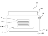
図6は、プラズマを用いない、高温雰囲気下での塩素ガスによるドライエッチングに用いる基板処理装置の断面構造を模式的に示す要部構成図である。
図6において、この基板処理装置31は、一または複数の半導体基板10が収容される処理チャンバ32、処理チャンバ32の上下に配設され、処理チャンバ32に対して加熱を行うための電気炉33、処理チャンバ32内で一または複数の半導体基板10を載置するためのステージ34およびボート35を有している。処理チャンバ32には、その内部に塩素系ガスなどのエッチングガスを導入するためのガス導入部36および、その内部から塩素系ガスなどのエッチングガスを排気するガス排気部37が設けられている。
この基板処理装置31は、処理チャンバ32内に一または複数の半導体基板10を配置し、加熱を行いながら塩素系ガスを内部に導入することによってドライエッチング処理を行うようになっている。代表的な条件は、大気圧下で加熱温度は摂氏800度である。
(実施形態3)
上記実施形態1では、ドライエッチングを行ってGaN層およびAlN層を除去して基板再生を行う場合について説明し、本実施形態2では、ドライエッチングおよびウエットエッチングを行いさらに超音波洗浄を行ってGaN層およびAlN層を除去しかつAlN層の残渣を除去して基板再生を行う場合について説明したが、本実施形態3では、Cl2ガスに対するSiCl4 高流量条件のICPドライエッチングにより、AlN層をエッチストップ層として残ったGaN層だけを除去する場合について説明する。
上記実施形態1では、ドライエッチングを行ってGaN層およびAlN層を除去して基板再生を行う場合について説明し、本実施形態2では、ドライエッチングおよびウエットエッチングを行いさらに超音波洗浄を行ってGaN層およびAlN層を除去しかつAlN層の残渣を除去して基板再生を行う場合について説明したが、本実施形態3では、Cl2ガスに対するSiCl4 高流量条件のICPドライエッチングにより、AlN層をエッチストップ層として残ったGaN層だけを除去する場合について説明する。
図7(a)~図7(c)は、本発明の実施形態3における再生基板の製造方法を説明するための基板断面図である。図8は、本発明の実施形態3における再生基板の製造方法の流れを示す工程図である。
まず、図7(a)および図8に示すように、ステップS31のGaN付きPSS基板受け入れ工程において、断面三角形状の表面繰り返し凹凸形状(PSS形状1a)を持つサファイヤ基板1上にバッファ層2(AlN層)の薄膜が形成され、その上層に表面が平坦な厚い窒化物半導体層3(GaN層)が形成された半導体基板10を、ICPドライエッチングを行う基板処理装置のチャンバ内の所定ステージ位置に導入する。この凹凸形状の深さは0.5μmである。
次に、図7(b)および図8に示すように、ステップS32の第2ドライエッチング工程において、Cl2ガスに対するSiCl4 ガスの低流量条件でICPドライエッチングを行う。即ち、Cl2 ガスに対するSiCl4ガスの混合比(体積比)が0.4で低選択比条件(レート比がGaN≒AlN≒Al2O3)となるようにCl2ガス流量に対してSiCl4 ガス流量を低ガス流量とし、Cl2 ガス流量を高くしてGaNに対しては高レートで素早くエッチングを進行させてICPドライエッチングを行う。このICPドライエッチングは凹凸形状のバッファ層2(ここではAlN層)の表面または手前(先端部近傍)またはその先端部まで行う。
これによって、凹凸形状のバッファ層2(AlN層)の表面または手前(先端部近傍)またはその先端部までの窒化物半導体層3(GaN層)をより早く除去する。このとき、SiCl4ガスとCl2 ガスの混合比は12:28で、SiCl4 ガス流量がCl2 ガス流量の半分(体積比)以下の値になっている。
その後、図7(c)および図8に示すように、ステップS33の第3ドライエッチング工程において、Cl2ガスに対するSiCl4 ガスの高流量条件でICPドライエッチングを行う。即ち、高選択比条件(レート比がGaN>Al2O3>AlN)となるようにCl2 ガス流量に対してSiCl4 ガス流量を高ガス流量とし、ICPドライエッチングを行う。SiCl4ガスは、バッファ層2(AlN層)に対してエッチングレートが非常に低いのでこれを利用し、SiCl4 ガスのガス流量を多くすることでバッファ層2のAlNをエッチストップ層として残った窒化物半導体層3A(GaN層)だけをエッチング除去することができる。
凹凸形状の上のバッファ層2(ここではAlN層)の表面または手前(先端部近傍)またはその先端部までで残った半導体基板10Aに対して、SiCl4高流量条件の高選択比条件で、ICPドライエッチングにより、バッファ層2のAlNをエッチストップ層としてその上の残った窒化物半導体層3A(GaN層)をエッチング除去する。このとき、SiCl4ガスとCl2 ガスの混合比は12:28から、56:28(「56」はCl2 ガスの「28」の2倍)としてSiCl4ガス流量をCl2 ガスの2倍(体積比)に上げている。この場合、Cl2 ガス流量に対してSiCl4ガス流量を半分以下(例えば0.4)から2倍に上げて高選択比条件(レート比がGaN>Al2O3>AlN)と調整することで、AlNをエッチストップ層としてその上の窒化物半導体層3のGaN層だけを残渣なく綺麗にエッチング除去してAlN層を残すことができる。
以上のSiCl4ガスの低流量条件はSiCl4 ガスがCl2 ガスの0.2~1倍(体積または重量)のガス流量(体積)に設定し、以上のSiCl4ガスの高流量条件はSiCl4 ガスがCl2 ガスの1~3倍(体積または重量)、より好ましくは1.5~3倍(エッチングストップの見極めがより容易)のガス流量(体積)に設定する。この場合に、SiCl4ガスの流量が多いほどバッファ層2(ここではAlN層)をエッチストップ層(エッチングストップ層)として用いることができる。
また、SiCl4ガスがCl2 ガスの3倍(体積混合比)を超えると、凹凸形状の深さ(0.5μm)との関係から、Cl2 ガスの濃度がうすくなって窒化物半導体層3A(GaN層)に対するエッチング速度が遅くなり過ぎるため、これ以上、SiCl4ガスの流量比を多くする意味がなくなる。表面の凹凸形状の深さが0.5μmよりも深くなると、SiCl4 ガスのCl2 ガスに対する流量比を3倍(体積混合比)よりも大きくする必要がある。表面の凹凸形状の深さ(段差)としては0.3μm~1μm程度のものを用いている。したがって、凹凸形状の深さが0.5μmの場合に、SiCl4ガスがCl2 ガスの1~3倍(体積または重量)のため、凹凸形状の深さが1μmの場合には、SiCl4 ガスがCl2ガスの1~6倍(体積または重量)になる。
一方、SiCl4ガスがCl2 ガスの半分程度、例えばここでは0.4程度としたが、SiCl4 ガスのCl2 ガスに対する混合比が0.2よりも下回ると、バッファ層2(AlN層)の先端部で一旦エッチングの進行を止める制御が難しくなる。もちろん、窒化物半導体層3(GaN層)をドライエッチングするのにSiCl4ガスの混合比は0であってもよい。ここでは具体的に、SiCl4 ガスの低流量条件は、SiCl4 ガスとCl2ガスの混合比が12:28に設定しており、SiCl4 ガスの高流量条件は、SiCl4 ガスとCl2ガスの混合比が56:28に設定している。
このように、ICPドライエッチングはCl2ガスとSiCl4 ガスとを混合することにより窒化物半導体層3(GaN層)を順次取り除いて、凹凸表面近傍のバッファ層2(AlN層)の表面または手前(先端部近傍)またはその先端位置までエッチング進行後、Cl2ガス流量に対するSiCl4 ガス流量比を増加させて、バッファ層2をエッチストップ層として窒化物半導体層3A(GaN層)だけを取り除く。これによって、GaN層の残渣なく、PSS形状1a上にバッファ層2(AlN層)の薄膜が残ったサファイヤ基板1(AlN付きPSS基板)を得ることができる。このようにして、バッファ層2(AlN層)の薄膜が残ったサファイヤ基板1(AlN付きPSS基板)を再生基板として製造することができる。
したがって、本実施形態3によれば、ICPドライエッチングをCl2ガスとSiCl4 ガスとを混合することにより行い、凹凸表面のバッファ層2(AlN層)の表面またはその近傍位置までエッチング進行後、SiCl4ガスの流量比を増加させるように調整して、バッファ層2(AlN層)をエッチストップ層として窒化物半導体層3(GaN膜)を除去するという化学的で簡便な除去方法で、従来のようにサファイヤ基板1の結晶性や凹凸形状に悪影響を与えず、AlN付きPSS基板を高品質で再生することができる。
この場合には、凹凸表面のバッファ層2(AlN層)をそのまま用いることができるので、バッファ層2(AlN層)を形成する工程を省略することができる。また、本実施形態3は、上記実施形態2のステップS20Aのウエットエッチング処理工程と、ステップS20Bの超音波残渣除去工程がないため、より少ない工程数で、再生基板を製造することができる。
(実施形態4)
上記実施形態3では、SiCl4高流量条件のICPドライエッチングによりバッファ層2(AlN層)をエッチストップ層として窒化物半導体層3(GaN膜)だけを除去する場合について説明したが、本実施形態4では、SiCl4高流量条件のICPドライエッチングによりバッファ層2(AlN層)をエッチストップ層として窒化物半導体層3(GaN層)を除去した後に、さらに、薬液(ウエットエッチング)によりバッファ層2(AlN層)を除去する場合について説明する。
上記実施形態3では、SiCl4高流量条件のICPドライエッチングによりバッファ層2(AlN層)をエッチストップ層として窒化物半導体層3(GaN膜)だけを除去する場合について説明したが、本実施形態4では、SiCl4高流量条件のICPドライエッチングによりバッファ層2(AlN層)をエッチストップ層として窒化物半導体層3(GaN層)を除去した後に、さらに、薬液(ウエットエッチング)によりバッファ層2(AlN層)を除去する場合について説明する。
図9(a)~図9(d)は、本発明の実施形態4における再生基板の製造方法を説明するための基板断面図である。図10は、本発明の実施形態4における再生基板の製造方法の流れを示す工程図である。
まず、図9(a)および図10に示すように、ステップS41のGaN付きPSS基板受け入れ工程において、表面繰り返し断面三角形状の凹凸形状(PSS形状1a)を持つサファイヤ基板1上にバッファ層2(AlN層)の薄膜が形成され、その上層に表面が平坦な厚い窒化物半導体層3(GaN層)が形成された半導体基板10を、ICPドライエッチングを行う基板処理装置のチャンバ内の所定ステージ位置に導入する。
次に、図9(b)および図10に示すように、ステップS42の第2ドライエッチング工程において、Cl2ガスの高流量条件で基板処理装置のチャンバ内にCl2 ガス(塩素ガス)を供給してCl2 ガス(塩素ガス)をプラズマ化して半導体基板10をICPドライエッチングして、凹凸形状の上方のバッファ層2(AlN層)の手前までの窒化物半導体層3(GaN層)をより早く除去する。このとき、SiCl4ガスとCl2 ガスの混合比は12:28で、Cl2 ガス流量がSiCl4 ガス流量の倍(体積比)以上になっており、SiCl4ガス流量がCl2 ガス流量の半分(体積比)以下になっている。
その後、図9(c)および図10に示すように、ステップS43の第3ドライエッチング工程において、高選択比条件(レート比がGaN>Al2O3>AlN)となるようにCl2ガス流量に対してSiCl4 ガス流量を高ガス流量として、ICPドライエッチングを行う。
凹凸形状の上方のバッファ層2(ここではAlN層)の表面または手前(先端
部近傍)またはその先端部までで残った半導体基板10Aに対して、SiCl4高流量条件の高選択比条件で、ICPドライエッチングにより、バッファ層2のAlNをエッチストップ層(エッチングストップ層)としてその上の残りの窒化物半導体層3AのGaN層をエッチング除去する。このとき、SiCl4ガスとCl2 ガスの混合比を56:28程度とする。この場合、Cl2 ガス流量に対してSiCl4ガス流量を1.5倍から3倍程度(ここでは2倍)に上げて高選択比条件(レート比がGaN>Al2O3>AlN)と調整することで、AlNをエッチストップ層としてその上の残った窒化物半導体層3AのGaN層だけをエッチング除去する。
部近傍)またはその先端部までで残った半導体基板10Aに対して、SiCl4高流量条件の高選択比条件で、ICPドライエッチングにより、バッファ層2のAlNをエッチストップ層(エッチングストップ層)としてその上の残りの窒化物半導体層3AのGaN層をエッチング除去する。このとき、SiCl4ガスとCl2 ガスの混合比を56:28程度とする。この場合、Cl2 ガス流量に対してSiCl4ガス流量を1.5倍から3倍程度(ここでは2倍)に上げて高選択比条件(レート比がGaN>Al2O3>AlN)と調整することで、AlNをエッチストップ層としてその上の残った窒化物半導体層3AのGaN層だけをエッチング除去する。
このように、ドライエッチングは塩素ガス(Cl2ガス)および塩素系ガス(SiCl4 ガス)により窒化物半導体層3(GaN層)を途中まで取り除いて、凹凸表面近傍のバッファ層2(AlN層)の表面または手前(先端部近傍)またはその先端部までエッチング進行後、Cl2ガスに対してSiCl4 ガスの混合比を増加して、バッファ層2をエッチストップ層として残った窒化物半導体層3Aだけを取り除く。これによって、PSS形状1a上にバッファ層2(AlN層)の薄膜が残ったサファイヤ基板1(AlN付きPSS基板)を得ることができる。
続いて、図9(d)および図10に示すように、ステップS44の薬液処理工程において、薬液として過酸化水素水(H2O2)と硫酸(H2SO4)との混合液を用いたウエットエッチングによりバッファ層2(AlN層)を除去する。
さらに、ステップS45の水洗工程において、サファイヤ基板1(PSS基板)に付いたバッファ層2(AlN層)の残渣を純水によって水洗いして除去する。ステップS46でこれを乾燥処理する。これらのステップS44の薬液処理工程およびステップS45の水洗工程、ステップS46の乾燥工程によりステップS40のウエットエッチング処理工程が構成される。
このように、バッファ層2をエッチストップ層として窒化物半導体層3だけを取り除いた後に、PSS形状1a上にバッファ層2(AlN層)の薄膜が残ったサファイヤ基板1(AlN付きPSS基板)に対してステップS40のウエットエッチング処理工程によりバッファ層2(AlN層)を取り除いて、ステップS47で表面が凹凸形状のPSS形状1aを持つサファイヤ基板1(PSS基板)得ることができる。このようにして、サファイヤ基板1(PSS基板)を再生基板として製造することができる。
したがって、本実施形態4によれば、化学的な簡便な除去方法で、サファイヤ基板の結晶性や凹凸形状に悪影響を与えずにPSS基板を高品質で再生できる。なお、このステップS40のウエットエッチング処理工程の後に上記実施形態2のステップS20Bの超音波残渣除去工程を行ってもよい。
図11は、上記実施形態1~4の各再生基板の製造方法の関係について説明するためのブロック図である。
図11に示すように、まず、ステップS51で、高流量条件の塩素ガス(Cl2)によって、ICPドライエッチングを行い、窒化物半導体層3(GaN層)および凹凸形状上のバッファ層2(AlN層)の薄膜を共に除去する。これが上記実施形態1の第1ドライエッチング工程である。
または、ステップS51において、高流量条件の塩素ガス(Cl2)をプラズマ化してICPドライエッチングを行って、凹凸形状の上方のバッファ層2(AlN層)の手前までの窒化物半導体層3(GaN層)だけを除去する。これが上記実施形態3の第2ドライエッチング工程である。
次に、ステップS52で、低流量条件の塩素ガス(Cl2)をプラズマ化してICPドライエッチングを行い、バッファ層2のAlNをエッチストップ層としてその上の窒化物半導体層3のGaN層をエッチング除去する。これが上記実施形態3の第3ドライエッチング工程である。PSS形状1aは上記実施形態1の第1ドライエッチング工程後のものに比べて良好である。
その後、ステップS53で硫酸処理を含むウエットエッチング処理工程を行い、ステップS54で超音波洗浄処理を含む超音波残渣除去工程を行ってGaN層およびAlN層を除去しかつAlN層の残渣を除去して基板再生を行う。これが、上記実施形態2のウエットエッチング工程および超音波残渣除去工程である。したがって、上記実施形態2では、上記実施形態1の第1ドライエッチング工程後に、ウエットエッチング工程および超音波残渣除去工程が順次実施される。
上記実施形態4は、Cl2ガス低流量条件のICPドライエッチングによりバッファ層2(AlN層)をエッチストップ層として窒化物半導体層3(GaN層)を除去した後に、さらに、ステップS53で硫酸処理を含むウエットエッチング工程を行って、バッファ層2(AlN層)を除去してPSS基盤を再生する。その後、ステップS54の超音波洗浄処理を含む超音波残渣除去工程を行ってより確実に表面上の残渣を除去するようにしてもよい。
このようにして、窒化物半導体層3(GaN層)が除去されて再生されたAlN付きPSS基板や、窒化物半導体層3(GaN層)およびバッファ層2(AlN層)が除去されたPSS基板を製造することができる。このようにして除去されたPSS基板やAlN付きPSS基板から、その上に上下のクラッド層間に発光層が挟まれた半導体発光素子が形成される。これについて図12を参照しながら説明する。
図12は、本発明の実施形態1~4の各再生基板の製造方法により製造された再生基板を用いた窒化物半導体発光素子の要部構成例を示す縦断面図である。
図12において、本実施形態1~4の各再生基板を用いた窒化物半導体発光素子20は、表面に凹凸形状(PSS形状1a)が形成された厚さ約1300μmの基板として例えばサファイヤ基板1上に、窒化アルミニウム(AlN)から成る膜厚約50nmのバッファ層2が成膜され、その上にノンドープのGaNから成る膜厚約10μmのノンドープGaN層である窒化物半導体層3が成膜されている。これらのサファイヤ基板1、バッファ層2および窒化物半導体層3(GaN層)から単結晶性基板の半導体基板10を構成している。ここでは、使用不能になった半導体基板10から、窒化物半導体層3(GaN層)およびバッファ層2(AlN層)のうちの少なくとも窒化物半導体層3(GaN層)を除去して上記実施形態1~4で得た再生基板(PSS基板またはAlN付きPSS基板)とし、この再生基板に再び、バッファ層2(AlN層)および窒化物半導体層3(GaN層)、または、窒化物半導体層3(GaN層)を付け替えて再生している。
さらに、この窒化物半導体発光素子20において、この単結晶性基板の半導体基板10上にシリコン(Si)を1×10¹⁸/cm3 ドープしたGaNからなる膜厚約5μmのn型コンタクト層41(高キャリヤ濃度n^+ 層)が形成されている。このn型コンタクト層41上に多重層51が形成され、この多重層51上には多重量子井戸構造の発光層52が形成されている。
さらに、この発光層52上に、Mgを2×10¹⁹/cm3 ドープした膜厚25nmのp型Al_0.15 Ga_0.85 Nからなるp型層である電子ブロック層6が形成され、この電子ブロック層6上に、Mgを8×10¹⁹ドープした膜厚100nmのp型GaNからなるp型コンタクト層42が形成されている。このp型コンタクト層42上には、金属蒸着による透光性薄膜電極7(ITO)が形成され、透光性薄膜電極7の一部上にp電極81が形成され、一方、n型コンタクト層41の端部上にはn電極82が形成されている。最上部には、SiO2膜よりなる保護膜9が形成されている。これによって、窒化物半導体発光素子20が構成されている。
なお、上記実施形態1~4では、表面に凹凸形状(PSS形状1a)が形成されたサファイヤ基板1を用いた場合について説明したが、これに限らず、サファイヤ基板1などの基板表面に凹凸加工が施されていない場合にも上記実施形態1~4の発明を適用することができる。
以上のように、本発明の好ましい実施形態1~4を用いて本発明を例示してきたが、本発明は、この実施形態1~4に限定して解釈されるべきものではない。本発明は、特許請求の範囲によってのみその範囲が解釈されるべきであることが理解される。当業者は、本発明の具体的な好ましい実施形態1~4の記載から、本発明の記載および技術常識に基づいて等価な範囲を実施することができることが理解される。本明細書において引用した特許、特許出願および文献は、その内容自体が具体的に本明細書に記載されているのと同様にその内容が本明細書に対する参考として援用されるべきであることが理解される。
本発明は、積層半導体層を成膜した積層半導体ウエハに対して、その基板を再び利用するために、積層半導体ウエハから積層半導体層を除去して再生基板を製造する再生基板の製造方法の分野において、簡便な方法で、基板の結晶性や表面凹凸形状に悪影響を与えずに、使用不可能になったGaN層付きPSS基板を品質良く再生することができる。
Claims (5)
- 基板上に窒化物半導体層が一または複数層形成された半導体基板に対してドライエッチングにより少なくとも該窒化物半導体層を除去する第1ドライエッチング工程を有する再生基板の製造方法。
- 前記基板と前記窒化物半導体層の間にバッファ層が設けられており、
該窒化物半導体層および該バッファ層を除去する前記ドライエッチングにより残った残渣を除去するウエットエッチング工程をさらに有する請求項1に記載の再生基板の製造方法。 - 前記ウエットエッチング工程で過酸化水素水と硫酸の混合液を用い、前記バッファ層はAlN層であり、
前記残渣としてAl化合物および該AlN層の残渣をさらに除去する超音波残渣除去工程を有し、該超音波残渣除去工程で用いる薬液は、過酸化水素水とアンモニア水の混合液であるかまたは、過酸化水素水、アンモニア水および純水の混合液である請求項2に記載の再生基板の製造方法。 - 前記基板と前記窒化物半導体層の間にバッファ層が設けられ、前記第1ドライエッチング工程は、ドライエッチングにより該バッファ層の表面またはその近傍位置まで該窒化物半導体層を除去する第2ドライエッチング工程と、該バッファ層をエッチストップ層としてドライエッチングにより残りの該窒化物半導体層を除去する第3ドライエッチング工程とを有する請求項1に記載の再生基板の製造方法。
- 前記第2ドライエッチング工程としてCl2ガスとSiCl4 ガスの混合ガスを用いて前記バッファ層の表面またはその近傍位置までエッチング進行後、前記第3ドライエッチング工程として該Cl2ガスに対するSiCl4 ガスの流量比を増加させるようにガス流量を調整する請求項4に記載の再生基板の製造方法。
Applications Claiming Priority (2)
| Application Number | Priority Date | Filing Date | Title |
|---|---|---|---|
| JP2013163442 | 2013-08-06 | ||
| JP2013-163442 | 2013-08-06 |
Publications (1)
| Publication Number | Publication Date |
|---|---|
| WO2015019539A1 true WO2015019539A1 (ja) | 2015-02-12 |
Family
ID=52460902
Family Applications (1)
| Application Number | Title | Priority Date | Filing Date |
|---|---|---|---|
| PCT/JP2014/003425 Ceased WO2015019539A1 (ja) | 2013-08-06 | 2014-06-26 | 再生基板の製造方法 |
Country Status (1)
| Country | Link |
|---|---|
| WO (1) | WO2015019539A1 (ja) |
Cited By (3)
| Publication number | Priority date | Publication date | Assignee | Title |
|---|---|---|---|---|
| JP2014045097A (ja) * | 2012-08-27 | 2014-03-13 | Sharp Corp | 再生基板の製造方法 |
| CN109509818A (zh) * | 2018-09-25 | 2019-03-22 | 华灿光电(苏州)有限公司 | 一种发光二极管的外延片及其制备方法 |
| CN111063615A (zh) * | 2019-12-30 | 2020-04-24 | 徐州同鑫光电科技股份有限公司 | 一种用于干法蚀刻中去除PSS衬底AlN涂层的方法 |
Citations (2)
| Publication number | Priority date | Publication date | Assignee | Title |
|---|---|---|---|---|
| JP2006518544A (ja) * | 2003-01-07 | 2006-08-10 | エス.オー.アイ.テック、シリコン、オン、インシュレター、テクノロジーズ | 薄層を除去した後の多層構造を備えるウェハのリサイクル |
| JP2013012719A (ja) * | 2011-05-31 | 2013-01-17 | Hitachi Kokusai Electric Inc | 基板処理装置および基板処理方法 |
-
2014
- 2014-06-26 WO PCT/JP2014/003425 patent/WO2015019539A1/ja not_active Ceased
Patent Citations (2)
| Publication number | Priority date | Publication date | Assignee | Title |
|---|---|---|---|---|
| JP2006518544A (ja) * | 2003-01-07 | 2006-08-10 | エス.オー.アイ.テック、シリコン、オン、インシュレター、テクノロジーズ | 薄層を除去した後の多層構造を備えるウェハのリサイクル |
| JP2013012719A (ja) * | 2011-05-31 | 2013-01-17 | Hitachi Kokusai Electric Inc | 基板処理装置および基板処理方法 |
Cited By (3)
| Publication number | Priority date | Publication date | Assignee | Title |
|---|---|---|---|---|
| JP2014045097A (ja) * | 2012-08-27 | 2014-03-13 | Sharp Corp | 再生基板の製造方法 |
| CN109509818A (zh) * | 2018-09-25 | 2019-03-22 | 华灿光电(苏州)有限公司 | 一种发光二极管的外延片及其制备方法 |
| CN111063615A (zh) * | 2019-12-30 | 2020-04-24 | 徐州同鑫光电科技股份有限公司 | 一种用于干法蚀刻中去除PSS衬底AlN涂层的方法 |
Similar Documents
| Publication | Publication Date | Title |
|---|---|---|
| TWI667697B (zh) | 基板處理系統及基板處理方法 | |
| KR101836152B1 (ko) | 식각 방법 | |
| JP6071514B2 (ja) | 静電チャックの改質方法及びプラズマ処理装置 | |
| CN111564405B (zh) | 用于处理基板的方法 | |
| US7776719B2 (en) | Method for manufacturing bonded wafer | |
| US7291286B2 (en) | Methods for removing black silicon and black silicon carbide from surfaces of silicon and silicon carbide electrodes for plasma processing apparatuses | |
| KR20090006265A (ko) | 플라즈마 세정 방법 | |
| KR100265289B1 (ko) | 플라즈마식각장치의 캐소우드 제조방법 및 이에 따라 제조되는 캐소우드 | |
| TWI445080B (zh) | Manufacturing method of semiconductor device | |
| JP2010500761A5 (ja) | ||
| JP2008160123A5 (ja) | ||
| JP2020043227A (ja) | プラズマ処理装置および半導体装置の製造方法 | |
| KR20210120058A (ko) | 광전 반도체칩의 제조 방법 및 이에 사용되는 본딩 웨이퍼 | |
| JP2021184505A (ja) | 基板処理システム及び基板処理方法 | |
| WO2015019539A1 (ja) | 再生基板の製造方法 | |
| JP2009185362A (ja) | 蒸着装置およびマスクのクリーニング方法 | |
| CN103000492B (zh) | 制造堆叠的氮化物半导体结构的方法以及制造氮化物半导体发光装置的方法 | |
| CN117552111A (zh) | 一种GaN单晶衬底的制备方法 | |
| US20050161435A1 (en) | Method of plasma etching | |
| CN100409407C (zh) | 用于晶圆的两层lto背面密封 | |
| JP4700652B2 (ja) | 層構造の製造方法 | |
| KR101132568B1 (ko) | 흄 발생없이 패턴을 형성하는 방법 | |
| TWI483350B (zh) | SOI wafer manufacturing method and glass cleaning method | |
| JP6301866B2 (ja) | 半導体製造方法 | |
| KR102296170B1 (ko) | 반도체 제조 공정을 이용한 질화물 반도체 발광소자 제조 방법 |
Legal Events
| Date | Code | Title | Description |
|---|---|---|---|
| 121 | Ep: the epo has been informed by wipo that ep was designated in this application |
Ref document number: 14834112 Country of ref document: EP Kind code of ref document: A1 |
|
| NENP | Non-entry into the national phase |
Ref country code: DE |
|
| NENP | Non-entry into the national phase |
Ref country code: JP |
|
| 122 | Ep: pct application non-entry in european phase |
Ref document number: 14834112 Country of ref document: EP Kind code of ref document: A1 |