WO2015019525A1 - カスコード型トランスコンダクタンス増幅器、可変利得回路およびこれらを備えたチューナシステム - Google Patents
カスコード型トランスコンダクタンス増幅器、可変利得回路およびこれらを備えたチューナシステム Download PDFInfo
- Publication number
- WO2015019525A1 WO2015019525A1 PCT/JP2014/002149 JP2014002149W WO2015019525A1 WO 2015019525 A1 WO2015019525 A1 WO 2015019525A1 JP 2014002149 W JP2014002149 W JP 2014002149W WO 2015019525 A1 WO2015019525 A1 WO 2015019525A1
- Authority
- WO
- WIPO (PCT)
- Prior art keywords
- variable gain
- transconductance amplifier
- transistor
- variable
- cascode
- Prior art date
- Legal status (The legal status is an assumption and is not a legal conclusion. Google has not performed a legal analysis and makes no representation as to the accuracy of the status listed.)
- Ceased
Links
Images







Classifications
-
- H—ELECTRICITY
- H03—ELECTRONIC CIRCUITRY
- H03G—CONTROL OF AMPLIFICATION
- H03G1/00—Details of arrangements for controlling amplification
- H03G1/0005—Circuits characterised by the type of controlling devices operated by a controlling current or voltage signal
- H03G1/0017—Circuits characterised by the type of controlling devices operated by a controlling current or voltage signal the device being at least one of the amplifying solid-state elements
- H03G1/0029—Circuits characterised by the type of controlling devices operated by a controlling current or voltage signal the device being at least one of the amplifying solid-state elements using field-effect transistors [FET]
-
- H—ELECTRICITY
- H03—ELECTRONIC CIRCUITRY
- H03G—CONTROL OF AMPLIFICATION
- H03G3/00—Gain control in amplifiers or frequency changers
- H03G3/20—Automatic control
- H03G3/30—Automatic control in amplifiers having semiconductor devices
- H03G3/3036—Automatic control in amplifiers having semiconductor devices in high-frequency amplifiers or in frequency-changers
-
- H—ELECTRICITY
- H03—ELECTRONIC CIRCUITRY
- H03F—AMPLIFIERS
- H03F1/00—Details of amplifiers with only discharge tubes, only semiconductor devices or only unspecified devices as amplifying elements
- H03F1/02—Modifications of amplifiers to raise the efficiency, e.g. gliding Class A stages, use of an auxiliary oscillation
- H03F1/0205—Modifications of amplifiers to raise the efficiency, e.g. gliding Class A stages, use of an auxiliary oscillation in transistor amplifiers
-
- H—ELECTRICITY
- H03—ELECTRONIC CIRCUITRY
- H03F—AMPLIFIERS
- H03F1/00—Details of amplifiers with only discharge tubes, only semiconductor devices or only unspecified devices as amplifying elements
- H03F1/02—Modifications of amplifiers to raise the efficiency, e.g. gliding Class A stages, use of an auxiliary oscillation
- H03F1/0205—Modifications of amplifiers to raise the efficiency, e.g. gliding Class A stages, use of an auxiliary oscillation in transistor amplifiers
- H03F1/0277—Selecting one or more amplifiers from a plurality of amplifiers
-
- H—ELECTRICITY
- H03—ELECTRONIC CIRCUITRY
- H03F—AMPLIFIERS
- H03F1/00—Details of amplifiers with only discharge tubes, only semiconductor devices or only unspecified devices as amplifying elements
- H03F1/08—Modifications of amplifiers to reduce detrimental influences of internal impedances of amplifying elements
- H03F1/22—Modifications of amplifiers to reduce detrimental influences of internal impedances of amplifying elements by use of cascode coupling, i.e. earthed cathode or emitter stage followed by earthed grid or base stage respectively
- H03F1/223—Modifications of amplifiers to reduce detrimental influences of internal impedances of amplifying elements by use of cascode coupling, i.e. earthed cathode or emitter stage followed by earthed grid or base stage respectively with MOSFET's
-
- H—ELECTRICITY
- H03—ELECTRONIC CIRCUITRY
- H03F—AMPLIFIERS
- H03F1/00—Details of amplifiers with only discharge tubes, only semiconductor devices or only unspecified devices as amplifying elements
- H03F1/32—Modifications of amplifiers to reduce non-linear distortion
- H03F1/3205—Modifications of amplifiers to reduce non-linear distortion in field-effect transistor amplifiers
-
- H—ELECTRICITY
- H03—ELECTRONIC CIRCUITRY
- H03F—AMPLIFIERS
- H03F3/00—Amplifiers with only discharge tubes or only semiconductor devices as amplifying elements
- H03F3/189—High-frequency amplifiers, e.g. radio frequency amplifiers
- H03F3/19—High-frequency amplifiers, e.g. radio frequency amplifiers with semiconductor devices only
- H03F3/193—High-frequency amplifiers, e.g. radio frequency amplifiers with semiconductor devices only with field-effect devices
-
- H—ELECTRICITY
- H03—ELECTRONIC CIRCUITRY
- H03F—AMPLIFIERS
- H03F3/00—Amplifiers with only discharge tubes or only semiconductor devices as amplifying elements
- H03F3/45—Differential amplifiers
- H03F3/45071—Differential amplifiers with semiconductor devices only
- H03F3/45076—Differential amplifiers with semiconductor devices only characterised by the way of implementation of the active amplifying circuit in the differential amplifier
- H03F3/45179—Differential amplifiers with semiconductor devices only characterised by the way of implementation of the active amplifying circuit in the differential amplifier using MOSFET transistors as the active amplifying circuit
-
- H—ELECTRICITY
- H03—ELECTRONIC CIRCUITRY
- H03G—CONTROL OF AMPLIFICATION
- H03G1/00—Details of arrangements for controlling amplification
- H03G1/0005—Circuits characterised by the type of controlling devices operated by a controlling current or voltage signal
- H03G1/0017—Circuits characterised by the type of controlling devices operated by a controlling current or voltage signal the device being at least one of the amplifying solid-state elements
- H03G1/0023—Circuits characterised by the type of controlling devices operated by a controlling current or voltage signal the device being at least one of the amplifying solid-state elements in emitter-coupled or cascode amplifiers
-
- H—ELECTRICITY
- H03—ELECTRONIC CIRCUITRY
- H03G—CONTROL OF AMPLIFICATION
- H03G1/00—Details of arrangements for controlling amplification
- H03G1/0005—Circuits characterised by the type of controlling devices operated by a controlling current or voltage signal
- H03G1/0088—Circuits characterised by the type of controlling devices operated by a controlling current or voltage signal using discontinuously variable devices, e.g. switch-operated
-
- H—ELECTRICITY
- H03—ELECTRONIC CIRCUITRY
- H03G—CONTROL OF AMPLIFICATION
- H03G3/00—Gain control in amplifiers or frequency changers
- H03G3/20—Automatic control
- H03G3/30—Automatic control in amplifiers having semiconductor devices
- H03G3/3052—Automatic control in amplifiers having semiconductor devices in bandpass amplifiers (H.F. or I.F.) or in frequency-changers used in a (super)heterodyne receiver
-
- H—ELECTRICITY
- H03—ELECTRONIC CIRCUITRY
- H03G—CONTROL OF AMPLIFICATION
- H03G3/00—Gain control in amplifiers or frequency changers
- H03G3/20—Automatic control
- H03G3/30—Automatic control in amplifiers having semiconductor devices
- H03G3/3052—Automatic control in amplifiers having semiconductor devices in bandpass amplifiers (H.F. or I.F.) or in frequency-changers used in a (super)heterodyne receiver
- H03G3/3063—Automatic control in amplifiers having semiconductor devices in bandpass amplifiers (H.F. or I.F.) or in frequency-changers used in a (super)heterodyne receiver using at least one transistor as controlling device, the transistor being used as a variable impedance device
-
- H—ELECTRICITY
- H03—ELECTRONIC CIRCUITRY
- H03F—AMPLIFIERS
- H03F2200/00—Indexing scheme relating to amplifiers
- H03F2200/451—Indexing scheme relating to amplifiers the amplifier being a radio frequency amplifier
-
- H—ELECTRICITY
- H03—ELECTRONIC CIRCUITRY
- H03F—AMPLIFIERS
- H03F2203/00—Indexing scheme relating to amplifiers with only discharge tubes or only semiconductor devices as amplifying elements covered by H03F3/00
- H03F2203/45—Indexing scheme relating to differential amplifiers
- H03F2203/45306—Indexing scheme relating to differential amplifiers the common gate stage implemented as dif amp eventually for cascode dif amp
Definitions
- the present disclosure relates to a cascode transconductance amplifier capable of reducing distortion and a variable gain circuit capable of reducing distortion and noise.
- a tuner system that receives a transmission signal composed of a plurality of channels, selects a desired channel, and performs demodulation is required to have low noise characteristics and low distortion characteristics.
- Japanese terrestrial digital television broadcasting (ISDB-T) is composed of a total of 40 channels from channel 13 (473.143 MHz) to channel 52 (707.143 MHz) with a signal bandwidth of 6 MHz per channel.
- the tuner system is required to have a sensitivity characteristic of ⁇ 80 dBm or less for each reception channel, while it is required to have an anti-jamming wave characteristic of 50 dBc or more with respect to the interference channel input level.
- the reception characteristics of such a tuner system are determined by the noise characteristics and distortion characteristics of a variable gain circuit that processes an RF signal immediately after reception by an antenna or the like.
- a tuner system mounted on a mobile terminal is required to reduce power consumption.
- variable gain circuit a configuration is disclosed in which an RF signal is switched to two paths and processed according to the signal strength (see, for example, Patent Document 1). Specifically, when the signal strength is low, the signal is amplified by the transconductance amplifier in the first path, while when the signal strength is high, the signal is attenuated by the attenuator in the second path. Thus, the signal is amplified by the transconductance amplifier provided in the path.
- the first route is turned on and the second route is turned off.
- the signal strength is high, the first route is turned off and the second route is turned off.
- an object of the present disclosure to provide a cascode transconductance amplifier capable of reducing distortion. It is another object of the present invention to provide a variable gain circuit capable of reducing noise, distortion, and power consumption.
- a cascode transconductance amplifier includes an amplification transistor connected to an input terminal, a cascode transistor having a source connected to a drain of the amplification transistor and a drain connected to an output terminal, the amplification transistor, and the cascode transistor. And a switching circuit for switching whether or not to connect the node connected to the fixed potential.
- connection node of the amplification transistor and the cascode transistor connected between the input terminal and the output terminal is connected to the fixed potential by the switching circuit.
- the switching circuit when a signal having a large amplitude is input, if the switching circuit is controlled so as to connect the connection node and the fixed potential, the signal passing through the amplifying transistor goes out to the fixed potential via the switching circuit. No leakage through the output end.
- the switching circuit when a signal having a small amplitude is input, if the switching circuit is controlled to release the connection between the connection node and the fixed potential, the signal can be sent to the output terminal through the amplification transistor and the cascode transistor.
- a transistor having a low threshold voltage can be used in the variable gain circuit.
- variable gain circuit having the first and second paths that are connected in parallel between the input terminal and the output terminal and that can amplify the signal
- first path is connected to the input terminal.
- a first variable attenuator for attenuating the input signal by a variable attenuation amount and connected between the first variable attenuator and the output terminal, and amplifies the output of the first variable attenuator.
- a second variable gain transconductance amplifier that amplifies the output of the second variable attenuator, and the input side of the second variable attenuator has the input terminal or the A first variable attenuator and the first variable gain transistor Scan is connected between the transconductance amplifier, the maximum gain of the first variable gain transconductance amplifier is greater than the maximum gain of the second variable gain transconductance amplifier.
- a variable attenuator and a variable gain transconductance amplifier are provided in the first path and the second path.
- the maximum gain of the first variable gain transconductance amplifier is set to be larger than the maximum gain of the second variable gain transconductance amplifier.
- the first variable gain transconductance amplifier since the input to the first variable gain transconductance amplifier is the output of the first variable attenuator, the first variable gain transconductance can be obtained even if the amplitude of the input signal is large.
- the signal input to the amplifier is attenuated by the first variable attenuator. Therefore, the first variable gain transconductance amplifier can be prevented from being intermittently turned on due to the amplitude of the signal, so that the signal can be reduced in distortion.
- variable gain transconductance amplifier since the amplitude of the signal handled by the first variable gain transconductance amplifier is reduced by the first variable attenuator, a transistor having a low threshold voltage can be used in the variable gain circuit.
- the first variable attenuator is turned off and the first variable gain transconductance amplifier is turned on in the first path, while the second path The variable attenuator is turned off and the second variable gain transconductance amplifier is turned on.
- the input signal is amplified without being attenuated in the first and second paths.
- the amplification by the first variable gain transconductance amplifier is large, noise can be reduced.
- the signal can be attenuated by first and second variable attenuators. Therefore, the amount of attenuation of the second variable attenuator can be reduced, and as a result, the area of the variable gain circuit can be reduced.
- the tuner system includes at least one of the cascode transconductance amplifier and the variable gain circuit.
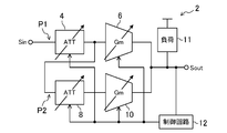
- FIG. 1 is a configuration diagram of a variable gain circuit according to the first embodiment.
- FIG. 2 is a configuration diagram of a variable gain circuit according to a modification of the first embodiment.
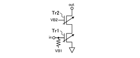
- FIG. 3 is a diagram illustrating a configuration example of the variable gain transconductance amplifier of FIG.
- FIG. 4 is a diagram showing another configuration example of the variable gain transconductance amplifier of FIG.
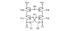
- FIG. 5 is a diagram showing another configuration example of the variable gain transconductance amplifier of FIG.
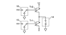
- FIG. 6 is a diagram showing another configuration example of Gm6 in FIG.
- FIG. 7 is a diagram showing another configuration example of Gm6 in FIG.
- FIG. 8 is a diagram showing another configuration example of Gm6 in FIG.
- FIG. 9 is a diagram illustrating a configuration example of the variable attenuator in FIG.
- FIG. 10 is a diagram illustrating another configuration example of the variable attenuator in FIG.
- FIG. 11 is a diagram illustrating another configuration example of the variable attenuator in FIG. 1.
- FIG. 12 is a diagram illustrating another configuration example of the variable attenuator in FIG.
- FIG. 13 is a diagram for explaining another example of the operation of the variable gain circuit of FIG.
- FIG. 14 is a configuration diagram of a tuner system according to the second embodiment.
- FIG. 1 is a configuration diagram of a variable gain circuit according to the first embodiment.
- the variable gain circuit 2 according to the present embodiment amplifies a signal input to the input terminal Sin and outputs it from the output terminal Sout.
- a signal received by an antenna or the like is input to the input terminal Sin.
- variable gain circuit 2 has a first path P1 and a second path P2 connected in parallel between the input terminal Sin and the output terminal Sout.
- the first path P1 includes a variable attenuator 4 (hereinafter abbreviated as ATT4) connected to the input terminal Sin, and a variable gain transconductance amplifier 6 (hereinafter referred to as Gm6) connected between the ATT4 and the output terminal Sout. Abbreviated).
- ATT4 variable attenuator 4
- Gm6 variable gain transconductance amplifier 6
- ATT4 is configured to be able to attenuate an input signal with a variable attenuation amount.
- Gm6 is configured to be capable of amplifying the output of ATT4 with a variable gain.
- the second path P2 includes a variable attenuator 8 (hereinafter abbreviated as ATT8) connected to the input terminal Sin and a variable gain transconductance amplifier 10 (hereinafter referred to as Gm10) connected between the ATT8 and the output terminal Sout. Abbreviated).
- ATT8 variable attenuator 8
- Gm10 variable gain transconductance amplifier 10
- ATT8 is configured to be able to attenuate an input signal with a variable attenuation amount.
- Gm10 is configured to amplify the output of ATT8 with a variable gain.
- the maximum gain of Gm10 is set to be smaller than the maximum gain of Gm6.
- the variable gain circuit 2 has a load 11 and a control circuit 12 connected to the output terminal Sout.
- the control circuit 12 controls the attenuation amounts of ATT4 and ATT8 and the gains of Gm6 and Gm10 based on, for example, a signal output from the output terminal Sout. Note that the signal level detected by the control circuit 12 may be other than the output terminal Sout of the variable gain circuit 2.
- variable gain circuit 2 when the signal received by the antenna is a weak electric field, that is, when the amplitude of the input signal to the input terminal Sin is small, the control circuit 12 controls to turn off both ATT4 and ATT8. As a result, ATT4 and ATT8 pass the input signal as they are.
- control circuit 12 controls the gains of Gm6 and Gm10 to be, for example, the maximum gain. Accordingly, Gm6 amplifies the input signal with a maximum gain larger than that of Gm10, and Gm10 amplifies the input signal with its own maximum gain.
- the maximum gain of Gm6 is set larger than the maximum gain of Gm10. Therefore, even when a signal having a low S / N ratio is input, the signal can be amplified by Gm6 without being attenuated by ATT4, so that noise can be reduced.
- the control circuit 12 controls to turn on ATT4 and ATT8. Therefore, ATT4 and ATT8 attenuate the input signal by a predetermined attenuation amount.
- control circuit 12 controls to turn on Gm10 while turning off Gm6.
- the input to Gm6 is attenuated by ATT4, it is possible to suppress Gm6 from being turned on due to the amplitude of the signal.
- the amplitude of the input signal is large, the amplitude of the signal input to Gm6 is suppressed by ATT4, so that Gm6 can be configured using a transistor having a low threshold voltage. Thereby, the power consumption of Gm6 can be reduced, and as a result, the power consumption of the variable gain circuit 2 can be reduced.
- ATT4 and Gm6 are provided in the first path P1, and ATT8 and Gm10 are provided in the second path P2, and the maximum gain of Gm6 is set to be larger than the maximum gain of Gm10. is doing.
- ATT4 and ATT8 are turned off and Gm6 and Gm10 are turned on.
- Gm6 is controlled to be turned off.
- variable gain circuit 2 capable of reducing power consumption while maintaining good noise characteristics and distortion characteristics.
- the input side of ATT8 is connected to input terminal Sin.
- the input side of ATT8 may be connected between ATT4 and Gm6. That is, ATT4 may be shared by the first route P1 and the second route P2.
- the input signal to the input terminal Sin is attenuated by ATT4 and ATT8 when the amplitude is large. Accordingly, the attenuation amount of ATT8 can be smaller than the attenuation amount of ATT4, so that the area of ATT8 can be reduced. As a result, the area of the variable gain circuit 2 can be reduced.
- the fixed potential is, for example, a ground potential.
- FIG. 3 is a diagram illustrating a configuration example of the variable gain transconductance amplifier of FIG.
- the variable gain transconductance amplifiers as Gm6 and Gm10 have a transistor Tr1 as an amplification transistor and a transistor Tr2 as a cascode transistor, as shown in FIG.
- the transistors Tr1 and Tr2 are Nch transistors, for example.
- the source of the transistor Tr1 is connected to the input terminal in of the variable gain transconductance amplifier, and the gate is connected to the bias voltage VB1. That is, the transistor Tr1 operates as a grounded-gate amplification transistor.
- the transistor Tr2 has a source connected to the drain of the transistor Tr1, a drain connected to the output terminal out of the variable gain transconductance amplifier, and a gate connected to the bias voltage VB2. Note that the magnitudes of the bias voltage VB1 and the bias voltage VB2 are arbitrary.
- the size of the amplification transistor Tr1 of Gm6 is set to be larger than the size of the amplification transistor Tr1 of Gm10. Thereby, the maximum gain of Gm6 can be made larger than the maximum gain of Gm10.
- FIG. 4 is a diagram showing another configuration example of the variable gain transconductance amplifier of FIG. In FIG. 4, differences from FIG. 3 will be mainly described.
- the transistor Tr1 has a gate connected to the input terminal in of the variable gain circuit, a bias element VB1 through a resistance element, and a source connected to a fixed potential. That is, the transistor Tr1 operates as a common source transistor.
- FIG. 5 is a diagram showing another configuration example of the variable gain transconductance amplifier of FIG.
- Gm6 and Gm10 of FIG. 1 may be configured to process differential signals.
- a circuit for generating a differential signal may be provided inside or preceding the variable gain transconductance amplifier.
- FIG. 5 differences from FIG. 3 will be mainly described.
- the variable gain transconductance amplifier of FIG. 5 includes a transistor Tr3, a transistor Tr4, and capacitive elements C1 and C2 in addition to the transistors Tr1 and Tr2.
- the source of the transistor Tr1 is connected to the input terminal in_p of the variable gain transconductance amplifier.
- the transistor Tr2 has a gate connected to the gate of the transistor Tr1, and a drain connected to the output terminal out_p of the variable gain transconductance amplifier.
- the transistor Tr3 is a differential amplification transistor that forms a differential pair with the transistor Tr1, and its source is connected to the differential input terminal in_n of the variable gain transconductance amplifier.
- the transistor Tr4 is a differential cascode transistor that forms a differential pair with the transistor Tr2.
- the source is connected to the drain of the transistor Tr3, and the drain is connected to the differential output terminal out_n of the variable gain transconductance amplifier.
- the source of the transistor Tr1 is connected to the gate of the transistor Tr3 via the capacitive element C1, and the source of the transistor Tr3 is connected to the gate of the transistor Tr1 via the capacitive element C2.
- the gates of the transistors Tr1 and Tr3 are connected to the bias voltage VB1, and the gates of the transistors Tr2 and Tr4 are connected to the bias voltage VB2.
- FIG. 6 is a diagram showing another configuration example of Gm6 in FIG. In FIG. 6, differences from FIG. 3 will be mainly described.
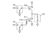
- the variable gain transconductance amplifier shown in FIG. 6 includes a switch 14 as a switching circuit, for example, an Nch transistor, in addition to the transistors Tr1 and Tr2.
- the variable gain transconductance amplifier also includes a switch 15 that connects the gate of the transistor Tr1 to a fixed potential or bias voltage VB1, and a switch 16 that connects the gate of the transistor Tr2 to a fixed potential or bias voltage VB2.
- the switch 14 switches whether to connect the intermediate node of the transistors Tr1 and Tr2 to a fixed potential.
- the switches 14, 15, and 16 are controlled by the control circuit 12 shown in FIG. Specifically, when Gm6 in FIG. 1 is in an off state, the control circuit 12 turns on the switch 14 to connect the intermediate node to a fixed potential. In addition, the control circuit 12 connects at least one of the switches 15 and 16 to a fixed potential.
- the control circuit 12 turns off the switch 14 to release the connection between the intermediate node and the fixed potential. Further, the switch 15 is controlled to be connected to the bias voltage VB1 and the switch 16 is connected to the bias voltage VB2.
- variable gain transconductance amplifier having the configuration of FIG. 6 as Gm6 of FIG. 1, the distortion characteristics of the variable gain circuit 2 can be further improved.
- FIG. 7 is a diagram showing another configuration example of Gm6 in FIG. In FIG. 7, differences from FIG. 4 will be mainly described.
- the variable gain transconductance amplifier of FIG. 7 has a switch 14 for switching whether or not to connect the intermediate node of the transistors Tr1 and Tr2 to a fixed potential in addition to the transistors Tr1 and Tr2. Further, the variable gain transconductance amplifier connects the other end of the resistance element connected to the gate of the transistor Tr1 to the fixed potential or the bias voltage VB1, and connects the gate of the transistor Tr2 to the fixed potential or the bias voltage VB2.
- a switch 16 is provided.
- FIG. 8 is a diagram showing another configuration example of Gm6 in FIG. In FIG. 8, differences from FIG. 5 will be mainly described.
- the variable gain transconductance amplifier of FIG. 8 has a switch 14 for switching whether or not to connect the intermediate nodes of the transistors Tr1 and Tr2 and the intermediate nodes of the transistors Tr3 and Tr4 to a fixed potential in addition to the transistors Tr1 to Tr4.
- the variable gain transconductance amplifier also includes a switch 15 that connects the gates of the transistors Tr1 and Tr3 to a fixed potential or bias voltage VB1, and a switch 16 that connects the gates of the transistors Tr2 and Tr4 to a fixed potential or bias voltage VB2. .
- the distortion characteristics of the variable gain circuit 2 can be improved. .
- any one of the switches 15 and 16 may be omitted.
- the bias voltages VB1 and VB2 may be connected to the gates of the transistors Tr1 and Tr2 and the transistors Tr3 and Tr4, respectively.
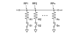
- FIG. 9 is a diagram illustrating a configuration example of the variable attenuator in FIG.
- the variable attenuator as ATT4 and ATT8 has a resistance element R and paths RP1 to RPn (n is a natural number).
- the resistance element R is provided between the input end in and the output end out of the variable attenuator.
- the paths RP1 to RPn are configured to be connected in parallel between the input terminal in and the output terminal out and the fixed potential.
- the paths RP1 to RPn include resistance elements R1 to Rn corresponding to the paths and switches S1 to Sn connected to the resistance elements R1 to Rn, respectively.
- the amount of attenuation becomes variable when the switches S1 to Sn are on / off controlled by the control circuit 12 of FIG.
- the input terminal in is connected to the input terminal Sin of the variable gain circuit 2 in FIG.
- FIG. 10 is a diagram illustrating another configuration example of the variable attenuator in FIG. As shown in FIG. 10, in order to keep the noise characteristics of the variable attenuator better, the resistor element R shown in FIG. 9 may be omitted, and the attenuator may be configured in combination with the input signal source impedance.
- FIG. 11 is a diagram illustrating another configuration example of the variable attenuator in FIG. 1. As shown in FIG. 11, the resistance elements R and R1 to Rn shown in FIG. 9 may be replaced with capacitive elements C and C1 to Cn.
- variable attenuators as ATT4 and ATT8 have a capacitive element C and paths CP1 to CPn as shown in FIG.
- the capacitive element C is provided between the input end in and the output end out of the variable attenuator.
- the paths CP1 to CPn are configured to be able to connect between the input terminal in and the output terminal out and the fixed potential in parallel.
- the paths CP1 to CPn include capacitive elements C1 to Cn corresponding to the respective paths, and switches S1 to Sn connected to the capacitive elements C1 to Cn, respectively.
- FIG. 12 is a diagram illustrating another configuration example of the variable attenuator in FIG.
- the variable attenuator shown in FIG. 12 has a combination of the variable attenuator shown in FIG. 9 and the variable attenuator shown in FIG.
- the variable attenuator includes paths RP1 to RPn having resistance elements R1 to Rn and switches SR1 to SRn corresponding thereto, capacitive element C, capacitive elements C1 to Cn, and switches SC1 to SCn corresponding thereto.
- Routes CP1 to CPn having
- the number of routes RP1 to RPn and the number of routes CP1 to CPn may be different.
- variable range of attenuation of the variable attenuator can be expanded.
- ATT4 and ATT8 may be configured by connecting a plurality of switch resistor circuits each including a resistor element and a switch in parallel, and the amount of attenuation may be variable by resistance voltage division.
- the ATT4 and ATT8 may be configured by connecting a plurality of switch capacitance circuits each including a capacitance element and a switch in parallel, and the attenuation may be variable by capacitance division.
- a switch resistance circuit and a switch capacitance circuit may be combined.
- a switch may be provided in any one of the routes RP1 to RPn and the routes CP1 to CPn.
- variable gain circuit 2 Next, another operation example of the variable gain circuit 2 according to the present embodiment will be described with reference to FIG.
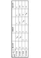
- FIG. 13 is a diagram for explaining another operation example of the variable gain circuit of FIG.
- FIG. 13 shows an example in which the gain of the variable gain circuit 2 is controlled so as to gradually change, and the control circuit 12 gradually changes the attenuation amounts of ATT4 and ATT8 and the gains of Gm6 and Gm10. Control.
- variable gain circuit 2 when the variable gain circuit 2 operates at the maximum gain, the attenuation amount of ATT4 and ATT8 is 0 dB (ATT4 and ATT8 are through modes), and the gains of Gm6 and Gm10 are 15 dB, for example, as the maximum gains, respectively. 4 dB.
- the attenuation amount of ATT4 gradually increases to, for example, ⁇ 5 dB, and the gain of Gm6 gradually decreases to 0 dB.
- the attenuation of ATT8 remains 0 dB and the gain of Gm10 remains 4 dB.
- the attenuation amount of ATT4 remains ⁇ 5 dB, while Gm6 is off, the attenuation amount of ATT8 is ⁇ 10 dB, for example, and the gain of Gm10 is ⁇ 10 dB.
- the two paths P1 and P2 are both turned on, and then the gain of one path is lowered to be sufficiently smaller than the other gain and then turned off.
- a seamless variable gain can be realized.
- the control for increasing the gain is the opposite, and the effect is the same.
- either of the timing for gradually increasing the attenuation amount of ATT4 and the timing for gradually decreasing the gain of Gm6 may be first. Further, either the timing for gradually increasing the attenuation amount of ATT8 or the timing for gradually decreasing the gain of Gm10 may be first.
- the operation shown in FIG. 13 shows an example in which the gain of the variable gain circuit 2 can be controlled to three or more values, and the attenuation amounts of ATT4 and ATT8 and the gains of Gm6 and Gm10 are changed.
- the number of steps is arbitrary.
- FIG. 14 shows a configuration of a tuner system according to the third embodiment.
- Each signal processing block except the antenna 21 in the figure can be integrated into an integrated circuit using a fine CMOS (Complementary Metal-Oxide Semiconductor) process.
- the signal strength of the RF signal received by the antenna 21 is adjusted by the variable gain circuit 2.
- the RF signal may be a wired signal input via a cable.
- the variable gain circuit 2 is according to the above-described embodiment.
- the RF signal processed by the variable gain circuit 2 is a local oscillation signal generated by a PLL (Phase Locked Loop) 23 and converted into a baseband signal by a mixer.
- the conversion method may be either the Low-IF method or the direct conversion method.
- the baseband signal is converted into a digital signal by an A / D converter (ADC) 26 after unnecessary high frequency components are sufficiently removed by a low pass filter (LPF) 25.
- ADC A / D converter
- LPF low pass filter
- demodulation processing and the like are performed in the digital signal processing unit (DSP) 27. Since the DSP 27 detects the input level of the RF signal, the variable characteristics of ATT4, ATT8 and Gm6, Gm10 in the variable gain circuit 2 of FIG. 1 can be controlled according to the detection result.
- a local oscillation signal of 470.143 MHz is output from the PLL 3, and the received RF signal is received by the mixer 24 with the reception frequency and local oscillation. It is converted into a baseband signal having an intermediate frequency of 3 MHz, which is a difference from the frequency.
- a high-frequency signal of 943.286 MHz which is the sum of the reception frequency and the local oscillation frequency, is also generated, but such a high-frequency component is sufficiently attenuated by the filtering process by the LPF 25.
- the signal band of the LPF 25 is 6 MHz, which is the same as the channel signal band.
- the tuner system since the RF signal immediately after reception by the antenna 21 is processed by the variable gain circuit 2 described above, good distortion characteristics and noise characteristics can be obtained, and power consumption can be reduced. It is.
- the ADC 26 may perform single-end conversion.
- the tuner system according to the present embodiment may have, for example, a cascode transconductance amplifier shown in FIG.
- the cascode transconductance amplifier according to the present disclosure can maintain good distortion characteristics.
- the variable gain circuit according to the present disclosure has good distortion characteristics and noise characteristics, and can reduce power consumption. Therefore, they are useful for stationary television apparatuses and portable terminals that receive analog broadcast waves and digital broadcast waves.
- Variable gain circuit 4 ATT (first variable attenuator) 6 Gm (first variable gain transconductance amplifier) 8 ATT (second variable attenuator) 10 Gm (second variable gain transconductance amplifier) 14 switches (switching circuit, third switching circuit) C, C1 to Cn Capacitors CP1 to CPn Path (fourth path) P1 First path P2 Second path R, R1 to Rn Resistance elements RP1 to RPn Path (third path) S1 to Sn switch (first switching circuit) SR1 to SRn, SC1 to SCn switch (second switching circuit) Tr1 transistor (amplification transistor) Tr2 transistor (cascode transistor) Tr3 transistor (differential amplification transistor) Tr4 transistor (differential cascode transistor)
Landscapes
- Engineering & Computer Science (AREA)
- Power Engineering (AREA)
- Physics & Mathematics (AREA)
- Nonlinear Science (AREA)
- Control Of Amplification And Gain Control (AREA)
- Amplifiers (AREA)
Abstract
可変利得トランスコンダクタンス増幅器は、入力端に接続された増幅トランジスタ(Tr1)と、ソースが増幅トランジスタのドレインに接続され、ドレインが出力端に接続されたカスコードトランジスタ(Tr2)と、増幅トランジスタとカスコードトランジスタとが接続されるノードを固定電位に接続するか否かを切り替える切替回路(14)とを備えている。また、可変利得回路(2)は、その可変利得トランスコンダクタンス増幅器を備えていてもよい。
Description
本開示は、低歪化が可能なカスコード型トランスコンダクタンス増幅器および低歪化と低雑音化が可能な可変利得回路に関する。
複数のチャンネルにより構成される送信信号を受信し、所望チャンネルを選択して復調を行うチューナシステムには低雑音特性と低歪特性が要求される。例えば、日本の地上波デジタルテレビ放送(ISDB-T)は1チャンネル当たり6MHzの信号帯域で第13チャンネル(473.143MHz)から第52チャンネル(707.143MHz)までの計40チャンネルで構成されており、チューナシステムには各受信チャンネルにおいて-80dBm以下の感度特性が求められる一方で、妨害チャンネル入力レベルに対して50dBc以上の耐妨害波特性が求められる。
こうしたチューナシステムの受信特性は、アンテナなどで受信した直後のRF信号を処理する可変利得回路の雑音特性と歪特性で決まる。一方、モバイル端末に搭載されるチューナシステムでは、低消費電力化が求められる。
可変利得回路として、信号強度に応じて、RF信号を2つの経路に切り替えて処理する構成が開示されている(例えば、特許文献1参照)。具体的には、信号強度が低い場合には、第1の経路におけるトランスコンダクタンス増幅器で信号が増幅される一方、信号強度が高い場合には、第2の経路における減衰器で信号が減衰されてから、当該経路に設けられたトランスコンダクタンス増幅器で信号が増幅される。
このように、信号強度が低い場合には、第1の経路をオン、かつ第2の経路をオフする一方、信号強度が高い場合には、第1の経路をオフ、かつ第2の経路をオンすることで、低雑音化および低歪化が図られている。
しかしながら、特許文献1の構成において信号強度が高い場合、オフしているはずの第1の経路のトランスコンダクタンス増幅器が、信号の振幅に起因して断続的にオンしてしまい、歪みを生じた信号が第1の経路から出力に漏れ出してしまうため、結果として、可変利得回路の歪特性が劣化することになる。また、トランスコンダクタンス増幅器としてゲート接地型増幅器を用いた場合には、入力インピーダンスの変動が顕著になるため、第2の経路におけるトランスコンダクタンス増幅器の入力で信号が歪んでしまう。これらのことは、可変利得回路の低消費電力化のために、閾値電圧が低いトランジスタを用いるとより顕著になるため、特許文献1の可変利得回路では低消費電力化が困難である。
かかる点に鑑みて、本開示は、低歪化が可能なカスコード型トランスコンダクタンス増幅器を提供することを課題とする。また、低雑音化および低歪化、ならびに低消費電力化が可能な可変利得回路を提供することを課題とする。
上記課題を解決するため本開示によって次のような解決手段を講じた。すなわち、カスコード型トランスコンダクタンス増幅器は、入力端に接続された増幅トランジスタと、ソースが前記増幅トランジスタのドレインに接続され、ドレインが出力端に接続されたカスコードトランジスタと、前記増幅トランジスタと前記カスコードトランジスタとが接続されるノードを固定電位に接続するか否かを切り替える切替回路とを備えている。
これによると、入力端と出力端との間に接続された、増幅トランジスタおよびカスコードトランジスタの接続ノードを、切替回路によって、固定電位に接続するか否かを切り替えることができる。
例えば、振幅が大きい信号が入力された場合、接続ノードと固定電位とを接続するように切替回路を制御すると、増幅トランジスタを通った信号は、切替回路を介して固定電位に抜けるため、カスコードトランジスタを通って出力端に漏れ出すことがない。一方、振幅が小さい信号が入力された場合、接続ノードと固定電位との接続を解除するように切替回路を制御すると、その信号を、増幅トランジスタおよびカスコードトランジスタを通して出力端に送出することができる。
これを前記第1の経路の増幅器として用いることで、第1の経路がオフ状態である場合に振幅の大きな信号が入力されても、第1の経路を通じて歪みを生じた信号が出力されず、前記可変利得回路の歪特性を良好に保つことができる。
さらに、大きな振幅の信号が入力されても歪み特性を良好に保てることから、可変利得回路において閾値電圧が低いトランジスタを用いることができる。
これらにより、可変利得回路において、低歪化および低消費電力化が可能となる。
また、入力端子と出力端子との間に並列接続された、信号の増幅が可能な第1および第2の経路を備えた可変利得回路は、前記第1の経路は、前記入力端子に接続され、入力された信号を可変減衰量で減衰させる第1の可変減衰器と、前記第1の可変減衰器と前記出力端子との間に接続され、前記第1の可変減衰器の出力を増幅する第1の可変利得トランスコンダクタンス増幅器とを有し、前記第2の経路は、入力された信号を可変減衰量で減衰させる第2の可変減衰器と、前記第2の可変減衰器と前記出力端子との間に接続され、前記第2の可変減衰器の出力を増幅する第2の可変利得トランスコンダクタンス増幅器とを有し、前記第2の可変減衰器の入力側は、前記入力端子、あるいは前記第1の可変減衰器と前記第1の可変利得トランスコンダクタンス増幅器との間に接続されており、前記第1の可変利得トランスコンダクタンス増幅器の最大利得は、前記第2の可変利得トランスコンダクタンス増幅器の最大利得よりも大きい。
これによると、第1の経路および第2の経路には、可変減衰器と可変利得トランスコンダクタンス増幅器とが設けられている。また、第1の可変利得トランスコンダクタンス増幅器の最大利得は、第2の可変利得トランスコンダクタンス増幅器の最大利得よりも大きくなるように設定されている。可変利得回路に信号が入力されると、その信号は、第1および第2の経路を経由して出力される。ここで、例えば、入力信号の振幅が大きい場合、第1の経路において、第1の可変減衰器をオンし、第1の可変利得トランスコンダクタンス増幅器をオフする一方、第2の経路において、第2の可変減衰器および第2の可変利得トランスコンダクタンス増幅器をともにオンする。
この場合、第1の経路において、第1の可変利得トランスコンダクタンス増幅器への入力は、第1の可変減衰器の出力であるため、入力信号の振幅が大きくても、第1の可変利得トランスコンダクタンス増幅器に入力される信号は、第1の可変減衰器によって減衰される。したがって、信号の振幅に起因して、第1の可変利得トランスコンダクタンス増幅器が断続的にオンするのを抑制することができるため、信号を低歪化することができる。
さらに、第1の可変利得トランスコンダクタンス増幅器で扱われる信号の振幅は第1の可変減衰器によって小さくなるため、可変利得回路において閾値電圧が低いトランジスタを用いることができる。
これらにより、可変利得回路において、低歪化および低消費電力化が可能となる。
また、例えば、入力信号の振幅が小さい場合、第1の経路において、第1の可変減衰器をオフし、第1の可変利得トランスコンダクタンス増幅器をオンする一方、第2の経路において、第2の可変減衰器をオフし、第2の可変利得トランスコンダクタンス増幅器をオンする。
この場合、第1および第2の経路において、入力信号は、減衰されずに増幅される。特に、第1の可変利得トランスコンダクタンス増幅器での増幅が大きいため、低雑音化が可能となる。
また、第2の可変減衰器の入力側を、第1の可変減衰器と第1の可変利得トランスコンダクタンス増幅器との間、すなわち第1の可変減衰器の出力側に接続するようにすれば、第2の経路において、信号を、第1および第2の可変減衰器によって減衰することができる。したがって、第2の可変減衰器の減衰量が少なくて済み、結果として、可変利得回路の面積を縮小することができる。
あるいは、チューナシステムは、上記カスコード型トランスコンダクタンス増幅器および上記可変利得回路の少なくとも一方を備えている。
これによると、チューナシステムにおいて、低雑音化、低歪化、および低消費電力化を図ることができる。
本開示によれば、低歪化が可能なカスコード型トランスコンダクタンス増幅器を提供することができるとともに、低雑音化、低歪化および低消費電力化が可能な可変利得回路を提供することができる。
<第1の実施形態>
図1は、第1の実施形態に係る可変利得回路の構成図である。本実施形態に係る可変利得回路2は、入力端子Sinに入力された信号を増幅して出力端子Soutから出力する。入力端子Sinには、アンテナ等で受信された信号が入力される。
図1は、第1の実施形態に係る可変利得回路の構成図である。本実施形態に係る可変利得回路2は、入力端子Sinに入力された信号を増幅して出力端子Soutから出力する。入力端子Sinには、アンテナ等で受信された信号が入力される。
具体的に、可変利得回路2は、入力端子Sinと出力端子Soutとの間に並列接続された、第1の経路P1および第2の経路P2を有する。
第1の経路P1は、入力端子Sinに接続された可変減衰器4(以下、ATT4と略記する)と、ATT4と出力端子Soutとの間に接続された可変利得トランスコンダクタンス増幅器6(以下、Gm6と略記する)とを有する。
ATT4は、入力された信号を可変減衰量で減衰可能に構成されている。Gm6は、ATT4の出力を可変利得で増幅可能に構成されている。
第2の経路P2は、入力端子Sinに接続された可変減衰器8(以下、ATT8と略記する)と、ATT8と出力端子Soutとの間に接続された可変利得トランスコンダクタンス増幅器10(以下、Gm10と略記する)とを有する。
ATT8は、入力された信号を可変減衰量で減衰可能に構成されている。Gm10は、ATT8の出力を可変利得で増幅可能に構成されている。そして、Gm10の最大利得は、Gm6の最大利得よりも小さくなるように設定されている。
なお、ATT4,ATT8およびGm6,Gm10の構成例については後述する。
また、可変利得回路2は、出力端子Soutに接続された負荷11と制御回路12とを有する。
制御回路12は、例えば出力端子Soutから出力される信号に基づいて、ATT4,ATT8の減衰量およびGm6,Gm10の利得を制御する。なお、制御回路12によって信号レベルを検出する場所は可変利得回路2の出力端子Sout以外であってもよい。
本実施形態に係る可変利得回路2の動作について説明する。例えば、アンテナで受信される信号が弱電界である場合、つまり、入力端子Sinへの入力信号の振幅が小さい場合、制御回路12は、ATT4,ATT8をともにオフするように制御する。これにより、ATT4,ATT8は入力された信号をそのままスルーする。
また、制御回路12は、Gm6,Gm10の利得が、例えば最大利得となるように制御する。これにより、Gm6は、入力信号をGm10よりも大きな最大利得で増幅するとともに、Gm10は、自身の最大利得で入力信号を増幅する。
そして、Gm6,Gm10の出力が合成され、合成された信号が出力端子Soutから出力される。
ここで、Gm6の最大利得はGm10の最大利得よりも大きく設定されている。したがって、S/N比が低い信号が入力された場合でも、ATT4で減衰させることなくGm6によって増幅可能であるため、低雑音化が可能である。
一方、アンテナで受信される信号が強電界である場合、つまり、入力端子Sinへの入力信号の振幅が大きい場合、制御回路12は、ATT4,ATT8をオンするように制御する。したがって、ATT4,ATT8は、入力信号を所定の減衰量で減衰する。
また、制御回路12は、Gm6をオフする一方、Gm10をオンするように制御する。このような制御により、Gm6への入力はATT4によって減衰されるため、信号の振幅に起因してGm6がオンするのを抑制することができる。これにより、Gm6の入力側で信号が歪んだり、歪みを生じた信号がオフ状態であるGm6から出力端子Soutへ漏れ出したりすることを抑制することができる。したがって、可変利得回路2の低歪化が可能である。
また、入力信号の振幅が大きい場合でもATT4によってGm6に入力される信号の振幅が抑圧されるため、閾値電圧が低いトランジスタを用いてGm6を構成することができる。これにより、Gm6の消費電力を低減することができ、結果として、可変利得回路2の低消費電力化を図ることができる。
以上、本実施形態によると、第1の経路P1にATT4とGm6とを設け、第2の経路P2にATT8とGm10とを設け、Gm6の最大利得がGm10の最大利得よりも大きくなるように設定している。そして、入力端子Sinへの入力信号の振幅が小さい場合には、ATT4,ATT8をオフするとともに、Gm6,Gm10をオンする一方、振幅が大きい場合には、ATT4,ATT8、およびGm10をオンするとともに、Gm6をオフするように制御している。
これにより、上述したように、雑音特性、歪特性を良好に保ちながらも、低消費電力化が可能な可変利得回路2を提供することができる。
なお、本実施形態では、ATT8の入力側を、入力端子Sinに接続しているが、図2に示すように、ATT8の入力側を、ATT4とGm6との間に接続してもよい。つまり、第1の経路P1および第2の経路P2によって、ATT4を共有するように構成してもよい。
これにより、第2の経路P2において、入力端子Sinへの入力信号は、その振幅が大きい場合、ATT4,ATT8によって減衰される。したがって、ATT8の減衰量はATT4の減衰量よりも少なくて済むため、ATT8の面積を削減することができる。結果として、可変利得回路2の面積を縮小することができる。
次に、Gm6およびGm10、ならびにATT4およびATT8の構成例について、図を参照しながら説明する。なお、以下の説明における固定電位とは、例えば接地電位である。
<Gm6およびGm10の構成例>
以下、Gm6およびGm10の具体例について、図3~図8を用いて説明する。
以下、Gm6およびGm10の具体例について、図3~図8を用いて説明する。
-構成例1-
図3は、図1の可変利得トランスコンダクタンス増幅器の構成例を示す図である。具体的に、Gm6,Gm10としての可変利得トランスコンダクタンス増幅器は、図3に示すように、増幅トランジスタとしてのトランジスタTr1と、カスコードトランジスタとしてのトランジスタTr2とを有する。トランジスタTr1,Tr2は、例えばNchトランジスタである。
図3は、図1の可変利得トランスコンダクタンス増幅器の構成例を示す図である。具体的に、Gm6,Gm10としての可変利得トランスコンダクタンス増幅器は、図3に示すように、増幅トランジスタとしてのトランジスタTr1と、カスコードトランジスタとしてのトランジスタTr2とを有する。トランジスタTr1,Tr2は、例えばNchトランジスタである。
トランジスタTr1は、ソースが可変利得トランスコンダクタンス増幅器の入力端inに接続され、ゲートがバイアス電圧VB1に接続されている。つまり、トランジスタTr1は、ゲート接地型増幅トランジスタとして動作する。
トランジスタTr2は、ソースがトランジスタTr1のドレインに接続され、ドレインが可変利得トランスコンダクタンス増幅器の出力端outに接続され、ゲートがバイアス電圧VB2に接続されている。なお、バイアス電圧VB1およびバイアス電圧VB2の大きさは任意である。
トランジスタTr2は、ソースがトランジスタTr1のドレインに接続され、ドレインが可変利得トランスコンダクタンス増幅器の出力端outに接続され、ゲートがバイアス電圧VB2に接続されている。なお、バイアス電圧VB1およびバイアス電圧VB2の大きさは任意である。
図1のGm6およびGm10として、図3の構成を用いることで、アンテナと図3の回路との整合(インピーダンスマッチング)が良好になる。
ここで、Gm6の増幅トランジスタTr1のサイズは、Gm10の増幅トランジスタTr1のサイズよりも大きくなるように設定されている。これにより、Gm6の最大利得を、Gm10の最大利得よりも大きくすることができる。
なお、Gm6,Gm10について、Gm6の最大利得がGm10の最大利得よりも大きくなるような構成であればよい。
-構成例2-
図4は、図1の可変利得トランスコンダクタンス増幅器の別の構成例を示す図である。図4では、図3との相違点ついて主に説明する。
図4は、図1の可変利得トランスコンダクタンス増幅器の別の構成例を示す図である。図4では、図3との相違点ついて主に説明する。
トランジスタTr1は、ゲートが可変利得回路の入力端inに接続されるとともに、抵抗素子を介してバイアス電圧VB1に接続され、ソースが固定電位に接続されている。つまり、トランジスタTr1は、ソース接地型トランジスタとして動作する。
このように、トランジスタTr1をソース接地型とすることで、可変利得トランスコンダクタンス増幅器の雑音特性が良好となる。
-構成例3-
図5は、図1の可変利得トランスコンダクタンス増幅器の別の構成例を示す図である。図5に示すように、図1のGm6およびGm10は、差動信号を処理するように構成されていてもよい。この場合、例えば、差動信号を生成する回路を可変利得トランスコンダクタンス増幅器の内部あるいは前段に設ければよい。図5では、図3との相違点について主に説明する。
図5は、図1の可変利得トランスコンダクタンス増幅器の別の構成例を示す図である。図5に示すように、図1のGm6およびGm10は、差動信号を処理するように構成されていてもよい。この場合、例えば、差動信号を生成する回路を可変利得トランスコンダクタンス増幅器の内部あるいは前段に設ければよい。図5では、図3との相違点について主に説明する。
図5の可変利得トランスコンダクタンス増幅器は、トランジスタTr1,Tr2に加え、トランジスタTr3と、トランジスタTr4と、容量素子C1,C2とを有する。
トランジスタTr1は、ソースが可変利得トランスコンダクタンス増幅器の入力端in_pに接続されている。トランジスタTr2は、ゲートがトランジスタTr1のゲートに接続され、ドレインが可変利得トランスコンダクタンス増幅器の出力端out_pに接続されている。
トランジスタTr3は、トランジスタTr1と差動対を構成する差動増幅トランジスタであり、ソースが可変利得トランスコンダクタンス増幅器の差動入力端in_nに接続されている。
トランジスタTr4は、トランジスタTr2と差動対を構成する差動カスコードトランジスタであり、ソースがトランジスタTr3のドレインに接続され、ドレインが可変利得トランスコンダクタンス増幅器の差動出力端out_nに接続されている。
また、トランジスタTr1のソースは、容量素子C1を介してトランジスタTr3のゲートに接続されており、トランジスタTr3のソースは容量素子C2を介してトランジスタTr1のゲートに接続されている。
トランジスタTr1,Tr3のゲートはバイアス電圧VB1に接続されており、トランジスタTr2,Tr4のゲートはバイアス電圧VB2に接続されている。
図1のGm6およびGm10を図5のように構成することで、図3および図4の構成の双方の効果を得ることができる。
なお、トランジスタTr1,Tr2の中間ノードを固定電位に接続可能な構成としてもよい。以下、このような構成について説明する。
-構成例4-
図6は、図1のGm6の別の構成例を示す図である。図6では、図3との相違点ついて主に説明する。
図6は、図1のGm6の別の構成例を示す図である。図6では、図3との相違点ついて主に説明する。
図6の可変利得トランスコンダクタンス増幅器は、トランジスタTr1,Tr2に加え、切替回路としての、例えばNchトランジスタであるスイッチ14を有する。また、可変利得トランスコンダクタンス増幅器は、トランジスタTr1のゲートを固定電位あるいはバイアス電圧VB1に接続するスイッチ15と、トランジスタTr2のゲートを固定電位あるいはバイアス電圧VB2に接続するスイッチ16とを有する。
スイッチ14は、トランジスタTr1,Tr2の中間ノードを固定電位に接続するか否かを切り替える。
スイッチ14,15,16は図1に示す制御回路12によって制御される。具体的に、図1のGm6がオフ状態である場合、制御回路12は、スイッチ14をオンして中間ノードを固定電位に接続する。また、制御回路12は、スイッチ15,16の少なくとも一方を、固定電位に接続する。
一方、Gm6がオン状態である場合、制御回路12は、スイッチ14をオフして中間ノードと固定電位との接続を解除する。また、スイッチ15をバイアス電圧VB1に、スイッチ16をバイアス電圧VB2に接続するように制御する。
このような構成により、オフ状態である場合に、入力端inから出力端outに歪みが漏れ出すことを抑制することができる。したがって、図6の構成の可変利得トランスコンダクタンス増幅器を、図1のGm6として用いることで、可変利得回路2の歪特性をより向上させることができる。
-構成例5-
図7は、図1のGm6の別の構成例を示す図である。図7では、図4との相違点について主に説明する。
図7は、図1のGm6の別の構成例を示す図である。図7では、図4との相違点について主に説明する。
図7の可変利得トランスコンダクタンス増幅器は、トランジスタTr1,Tr2に加え、トランジスタTr1,Tr2の中間ノードを固定電位に接続するか否かを切り替えるスイッチ14を有する。また、可変利得トランスコンダクタンス増幅器は、トランジスタTr1のゲートに接続された抵抗素子の他端を固定電位あるいはバイアス電圧VB1に接続するスイッチ15、およびトランジスタTr2のゲートを固定電位あるいはバイアス電圧VB2に接続するスイッチ16を有する。
-構成例6-
図8は、図1のGm6の別の構成例を示す図である。図8では、図5との相違点について主に説明する。
図8は、図1のGm6の別の構成例を示す図である。図8では、図5との相違点について主に説明する。
図8の可変利得トランスコンダクタンス増幅器は、トランジスタTr1~Tr4に加え、トランジスタTr1,Tr2の中間ノード、およびトランジスタTr3,Tr4の中間ノードを固定電位接続するか否かを切り替えるスイッチ14を有する。
また、可変利得トランスコンダクタンス増幅器は、トランジスタTr1,Tr3のゲートを固定電位あるいはバイアス電圧VB1に接続するスイッチ15と、トランジスタTr2,Tr4のゲートを固定電位あるいはバイアス電圧VB2に接続するスイッチ16とを有する。
以上、オフ状態にGm6における図6~図8のトランジスタTr1,Tr2、および図8のトランジスタTr3,Tr4の中間ノードを接地可能とすることで、可変利得回路2の歪特性を向上させることができる。
なお、図6~図8において、スイッチ15,16のいずれかを省略してもよい。この場合、トランジスタTr1,Tr2、およびトランジスタTr3,Tr4のゲートには、それぞれのバイアス電圧VB1,VB2が接続されていてもよい。
<ATT4およびATT8の構成例>
次に、ATT4およびATT8の具体例について、図9~図12を用いて説明する。
次に、ATT4およびATT8の具体例について、図9~図12を用いて説明する。
-構成例1-
図9は、図1の可変減衰器の構成例を示す図である。ATT4,ATT8としての可変減衰器は、図9に示すように、抵抗素子Rと、経路RP1~RPn(nは自然数)とを有する。
図9は、図1の可変減衰器の構成例を示す図である。ATT4,ATT8としての可変減衰器は、図9に示すように、抵抗素子Rと、経路RP1~RPn(nは自然数)とを有する。
抵抗素子Rは、可変減衰器の入力端inおよび出力端outとの間に設けられる。経路RP1~RPnは、入力端inおよび出力端outの間と固定電位との間を並列に接続可能に構成されている。
具体的に、経路RP1~RPnは、それぞれに対応する抵抗素子R1~Rnと、抵抗素子R1~Rnのそれぞれに接続されるスイッチS1~Snとを有する。可変減衰器は、図1の制御回路12によってスイッチS1~Snがオンオフ制御されることで、減衰量が可変となる。
なお、入力端inは、図1の可変利得回路2の入力端子Sinに接続される。
-構成例2-
図10は、図1の可変減衰器の別の構成例を示す図である。図10に示すように、可変減衰器の雑音特性をより良好に保つために、図9に示す抵抗素子Rを省略し、入力信号源インピーダンスとの組み合わせで減衰器を構成してもよい。
図10は、図1の可変減衰器の別の構成例を示す図である。図10に示すように、可変減衰器の雑音特性をより良好に保つために、図9に示す抵抗素子Rを省略し、入力信号源インピーダンスとの組み合わせで減衰器を構成してもよい。
-構成例3-
図11は、図1の可変減衰器の別の構成例を示す図である。図11に示すように、図9に示す抵抗素子R,R1~Rnを容量素子C,C1~Cnに換えてもよい。
図11は、図1の可変減衰器の別の構成例を示す図である。図11に示すように、図9に示す抵抗素子R,R1~Rnを容量素子C,C1~Cnに換えてもよい。
具体的に、ATT4およびATT8としての可変減衰器は、図11に示すように、容量素子Cと、経路CP1~CPnとを有する。
容量素子Cは、可変減衰器の入力端inおよび出力端outとの間に設けられる。経路CP1~CPnは、入力端inおよび出力端outの間と固定電位との間を並列に接続可能に構成されている。
経路CP1~CPnは、それぞれに対応する容量素子C1~Cnと、容量素子C1~Cnのそれぞれに接続されるスイッチS1~Snとを有する。
-構成例4-
図12は、図1の可変減衰器の別の構成例を示す図である。図12に示す可変減衰器は、図9の可変減衰器と図11の可変減衰器とを組み合わせた構成となっている。具体的に、可変減衰器は、抵抗素子R1~Rnおよびこれらに対応するスイッチSR1~SRnを有する経路RP1~RPnと、容量素子Cと、容量素子C1~Cnおよびこれらに対応するスイッチSC1~SCnを有する経路CP1~CPnとを有していてもよい。
図12は、図1の可変減衰器の別の構成例を示す図である。図12に示す可変減衰器は、図9の可変減衰器と図11の可変減衰器とを組み合わせた構成となっている。具体的に、可変減衰器は、抵抗素子R1~Rnおよびこれらに対応するスイッチSR1~SRnを有する経路RP1~RPnと、容量素子Cと、容量素子C1~Cnおよびこれらに対応するスイッチSC1~SCnを有する経路CP1~CPnとを有していてもよい。
なお、経路RP1~RPnの数と経路CP1~CPnの数は異なっていてもよい。
このように構成することで、可変減衰器の減衰量の可変範囲を拡張することができる。
以上、図9~図12に示すように、ATT4,ATT8は、抵抗素子とスイッチからなるスイッチ抵抗回路を複数個並列に接続して構成し、抵抗分圧によって減衰量を可変としてもよい。また、ATT4,ATT8は、容量素子とスイッチからなるスイッチ容量回路を複数個並列に接続して構成し、容量分圧によって減衰量を可変としてもよい。さらに、スイッチ抵抗回路とスイッチ容量回路とを組み合わせてもよい。
また、図9~図12において、経路RP1~RPnおよび経路CP1~CPnのいずれか1つの経路にスイッチが設けられていればよい。
また、図9~図12において、可変減衰器の入力端inおよび出力端outの間と固定電位との間の経路は1つでもよく、その経路に、抵抗素子および容量素子の少なくとも一方と、スイッチとが設けられていればよい。つまり、減衰器の減衰量が可変であるような構成であればよい。
次に、本実施形態に係る可変利得回路2の別の動作例について、図13を用いて説明する。
図13は、図1の可変利得回路の別の動作例を説明するための図である。図13は、可変利得回路2の利得が徐々に変化するように制御される場合の例であり、制御回路12は、ATT4,ATT8の減衰量およびGm6,Gm10の利得を徐々に変化させるように制御する。
具体的に、可変利得回路2が最大利得で動作している場合、ATT4,ATT8の減衰量は0dB(ATT4,ATT8はスルーモード)であり、Gm6,Gm10の利得はそれぞれ最大利得として例えば15dB,4dBである。
この状態から、可変利得回路2の利得が低下して中間利得になる場合、ATT4の減衰量は徐々に増加して例えば-5dBとなり、Gm6の利得は徐々に低下して0dBとなる。このとき、ATT8の減衰量は0dB、Gm10の利得は4dBのままである。
さらに、可変利得回路2の利得が低下して最小利得になる場合、ATT4の減衰量は-5dBのままである一方、Gm6はオフ、ATT8の減衰量は例えば-10dB、Gm10の利得は例えば-10dBとなる。
以上のように、可変利得回路2の利得を減衰させる際に、2つの経路P1,P2が共にオンした状態から、一方の経路の利得を他方の利得に比べて十分小さくなるまで下げてからオフ状態に遷移させることで、シームレスな利得可変が実現できる。
なお、利得を増大させる場合の制御はこの逆であり、効果は同様である。
ここで、特許文献1の構成では、信号強度に応じて2つの経路を切り替えているため、経路の切り替えのタイミングにおいて、可変利得回路の利得や入出力信号の位相関係が大きく変動してしまう。その結果、信号品質が大きく劣化してしまう。
これに対して、可変利得回路2の利得を図13に示すように制御することで、このような問題を抑制することができる。
なお、図13において、ATT4の減衰量を徐々に増加させるタイミング、およびGm6の利得を徐々に減少させるタイミングは、どちらが先でもよい。また、ATT8の減衰量を徐々に増加させるタイミング、およびGm10の利得を徐々に減少させるタイミングは、どちらが先でもよい。
また、図13に示す動作は、可変利得回路2の利得が、3値以上に制御可能であることの例を示すものであり、ATT4,ATT8の減衰量、およびGm6,Gm10の利得を変化させる際のステップ数は任意である。
<第2の実施形態>
図14は、第3の実施形態に係るチューナシステムの構成を示す。図中のアンテナ21を除く各信号処理ブロックは微細CMOS(Complementary Metal-Oxide Semiconductor)プロセスを用いて集積回路化することができる。アンテナ21で受信したRF信号は可変利得回路2によって信号強度が調整される。RF信号はケーブルを介して入力される有線信号であってもよい。可変利得回路2は、上述した実施形態に係るものである。
図14は、第3の実施形態に係るチューナシステムの構成を示す。図中のアンテナ21を除く各信号処理ブロックは微細CMOS(Complementary Metal-Oxide Semiconductor)プロセスを用いて集積回路化することができる。アンテナ21で受信したRF信号は可変利得回路2によって信号強度が調整される。RF信号はケーブルを介して入力される有線信号であってもよい。可変利得回路2は、上述した実施形態に係るものである。
可変利得回路2で処理されたRF信号は、PLL(Phase Locked Loop)23が生成した局部発振信号でミキサによってベースバンド信号に変換される。変換方式はLow-IF方式およびダイレクトコンバージョン方式のいずれでもよい。ベースバンド信号はローパスフィルタ(LPF)25によって不要な高周波成分が十分に取り除かれた後にA/D変換器(ADC)26でデジタル信号に変換される。そして、最終的にデジタル信号処理部(DSP)27において復調処理などが行われる。DSP27ではRF信号の入力レベルが検出されるため、当該検出結果に応じて図1の可変利得回路2におけるATT4,ATT8やGm6,Gm10の可変特性を制御することができる。
例えば、日本の地上波デジタルテレビ放送における第13チャンネル(473.143MHz)を受信する場合、PLL3からは470.143MHzの局部発振信号が出力され、受信したRF信号はミキサ24において受信周波数と局部発振周波数との差である3MHzの中間周波数のベースバンド信号に変換される。このとき、受信周波数と局部発振周波数との和である943.286MHzの高周波信号も発生するが、そのような高周波成分はLPF25によるフィルタリング処理で十分に減衰する。例えば、LPF25の信号帯域はチャンネルの信号帯域と同じ6MHzである。他のチャンネル受信時はPLL23の発振周波数が希望チャンネルに応じて変化する。
本実施形態に係るチューナシステムでは、アンテナ21の受信直後のRF信号を、上述した可変利得回路2で処理するため、良好な歪特性および雑音特性を得ることができるとともに、低消費電力化が可能である。
なお、チューナシステムで差動信号を扱う場合には、例えばADC26でシングルエンド変換を行うようにしてもよい。
また、本実施形態に係るチューナシステムは、例えば図6に示すカスコード型トランスコンダクタンス増幅器を有していてもよい。
本開示に係るカスコード型トランスコンダクタンス増幅器は、歪特性を良好に保つことができる。また、本開示に係る可変利得回路は、良好な歪特性および雑音特性で、かつ低消費電力化が可能である。したがって、これらは、アナログ放送波およびデジタル放送波を受信する据え置き型のテレビジョン装置や携帯型端末などに有用である。
2 可変利得回路
4 ATT(第1の可変減衰器)
6 Gm(第1の可変利得トランスコンダクタンス増幅器)
8 ATT(第2の可変減衰器)
10 Gm(第2の可変利得トランスコンダクタンス増幅器)
14 スイッチ(切替回路、第3の切替回路)
C,C1~Cn 容量素子
CP1~CPn 経路(第4の経路)
P1 第1の経路
P2 第2の経路
R,R1~Rn 抵抗素子
RP1~RPn 経路(第3の経路)
S1~Sn スイッチ(第1の切替回路)
SR1~SRn,SC1~SCn スイッチ(第2の切替回路)
Tr1 トランジスタ(増幅トランジスタ)
Tr2 トランジスタ(カスコードトランジスタ)
Tr3 トランジスタ(差動増幅トランジスタ)
Tr4 トランジスタ(差動カスコードトランジスタ)
4 ATT(第1の可変減衰器)
6 Gm(第1の可変利得トランスコンダクタンス増幅器)
8 ATT(第2の可変減衰器)
10 Gm(第2の可変利得トランスコンダクタンス増幅器)
14 スイッチ(切替回路、第3の切替回路)
C,C1~Cn 容量素子
CP1~CPn 経路(第4の経路)
P1 第1の経路
P2 第2の経路
R,R1~Rn 抵抗素子
RP1~RPn 経路(第3の経路)
S1~Sn スイッチ(第1の切替回路)
SR1~SRn,SC1~SCn スイッチ(第2の切替回路)
Tr1 トランジスタ(増幅トランジスタ)
Tr2 トランジスタ(カスコードトランジスタ)
Tr3 トランジスタ(差動増幅トランジスタ)
Tr4 トランジスタ(差動カスコードトランジスタ)
Claims (20)
- 入力端に接続された増幅トランジスタと、
ソースが前記増幅トランジスタのドレインに接続され、ドレインが出力端に接続されたカスコードトランジスタと、
前記増幅トランジスタと前記カスコードトランジスタとが接続されるノードを固定電位に接続するか否かを切り替える切替回路とを備えている
ことを特徴とするカスコード型トランスコンダクタンス増幅器。 - 請求項1のカスコード型トランスコンダクタンス増幅器において、
前記切替回路が前記ノードと前記固定電位とを接続しているとき、前記増幅トランジスタおよび前記カスコードトランジスタの少なくとも一方はオフ状態である
ことを特徴とするカスコード型トランスコンダクタンス増幅器。 - 請求項1のカスコード型トランスコンダクタンス増幅器において、
前記増幅トランジスタのソースは前記入力端に接続され、ゲートはバイアス可能に構成されている
ことを特徴とするカスコード型トランスコンダクタンス増幅器。 - 請求項1のカスコード型トランスコンダクタンス増幅器において、
前記増幅トランジスタのゲートは前記入力端に接続されるとともにバイアスされ、ソースは前記固定電位に接続されている
ことを特徴とするカスコード型トランスコンダクタンス増幅器。 - 請求項1のカスコード型トランスコンダクタンス増幅器において、
前記増幅トランジスタと差動対を構成し、前記入力端に対する差動入力端に接続された差動増幅トランジスタと、
前記カスコードトランジスタと差動対を構成し、ソースが前記差動増幅トランジスタのドレインに接続され、ドレインが前記出力端に対する差動出力端に接続された差動カスコードトランジスタとを備え、
前記増幅トランジスタおよび前記差動増幅トランジスタはそれぞれ、一方のソースが容量素子を介して他方のゲートに接続され、かつゲートがバイアス可能に構成されており、
前記切替回路は、前記差動増幅トランジスタと前記差動カスコードトランジスタとが接続されるノードを固定電位に接続するか否かを切り替える
ことを特徴とするカスコード型トランスコンダクタンス増幅器。 - 入力端子と出力端子との間に並列接続された、信号の増幅が可能な第1および第2の経路を備えた可変利得回路であって、
前記第1の経路は、
前記入力端子に接続され、入力された信号を可変減衰量で減衰させる第1の可変減衰器と、
前記第1の可変減衰器と前記出力端子との間に接続され、前記第1の可変減衰器の出力を増幅する第1の可変利得トランスコンダクタンス増幅器とを有し、
前記第2の経路は、
入力された信号を可変減衰量で減衰させる第2の可変減衰器と、
前記第2の可変減衰器と前記出力端子との間に接続され、前記第2の可変減衰器の出力を増幅する第2の可変利得トランスコンダクタンス増幅器とを有し、
前記第2の可変減衰器の入力側は、前記入力端子、あるいは前記第1の可変減衰器と前記第1の可変利得トランスコンダクタンス増幅器との間に接続されており、
前記第1の可変利得トランスコンダクタンス増幅器の最大利得は、前記第2の可変利得トランスコンダクタンス増幅器の最大利得よりも大きい
ことを特徴とする可変利得回路。 - 請求項6の可変利得回路において、
前記第1の可変利得トランスコンダクタンス増幅器は、
ソースが当該第1の可変利得トランスコンダクタンス増幅器の入力端に接続され、ゲートがバイアスされた第1の増幅トランジスタと、
ソースが前記第1の増幅トランジスタのドレインに接続され、ドレインが当該第1の可変利得トランスコンダクタンス増幅器の出力端に接続された第1のカスコードトランジスタとを有し、
前記第2の可変利得トランスコンダクタンス増幅器は、
ソースが当該第2の可変利得トランスコンダクタンス増幅器の入力端に接続され、ゲートがバイアスされた第2の増幅トランジスタと、
ソースが前記第2の増幅トランジスタのドレインに接続され、ドレインが当該第2の可変利得トランスコンダクタンス増幅器の出力端に接続された第2のカスコードトランジスタとを有する
ことを特徴とする可変利得回路。 - 請求項6の可変利得回路において、
前記第1の可変利得トランスコンダクタンス増幅器は、
ゲートが当該第1の可変利得トランスコンダクタンス増幅器の入力端に接続されるとともにバイアスされ、ソースが固定電位に接続された第1の増幅トランジスタと、
ソースが前記第1の増幅トランジスタのドレインに接続され、ドレインが当該第1の可変利得トランスコンダクタンス増幅器の出力端に接続された第1のカスコードトランジスタとを有し、
前記第2の可変利得トランスコンダクタンス増幅器は、
ゲートが当該第2の可変利得トランスコンダクタンス増幅器の入力端に接続されるとともにバイアスされ、ソースが前記固定電位に接続された第2の増幅トランジスタと、
ソースが前記第2の増幅トランジスタのドレインに接続され、ドレインが当該第2の可変利得トランスコンダクタンス増幅器の出力端に接続された第2のカスコードトランジスタとを有する
ことを特徴とする可変利得回路。 - 請求項6の可変利得回路において、
前記第1の可変利得トランスコンダクタンス増幅器は、
当該第1の可変利得トランスコンダクタンス増幅器の入力端に接続された第1の増幅トランジスタと、
ソースが前記第1の増幅トランジスタのドレインに接続され、ドレインが当該第1の可変利得トランスコンダクタンス増幅器の出力端に接続された第1のカスコードトランジスタと、
前記第1の増幅トランジスタと差動対を構成し、当該第1の可変利得トランスコンダクタンス増幅器の入力端に対する差動入力端に接続された第1の差動増幅トランジスタと、
前記第1のカスコードトランジスタと差動対を構成し、ソースが前記第1の差動増幅トランジスタのドレインに接続され、ドレインが当該第1の可変利得トランスコンダクタンス増幅器の出力端に対する差動出力端に接続された第1の差動カスコードトランジスタとを有し、
前記第2の可変利得トランスコンダクタンス増幅器は、
当該第2の可変利得トランスコンダクタンス増幅器の入力端に接続された第2の増幅トランジスタと、
ソースが前記第2の増幅トランジスタのドレインに接続され、ドレインが当該第2の可変利得トランスコンダクタンス増幅器の出力端に接続された第2のカスコードトランジスタと、
前記第2の増幅トランジスタと差動対を構成し、当該第2の可変利得トランスコンダクタンス増幅器の入力端に対する差動入力端に接続された第2の差動増幅トランジスタと、
前記第2のカスコードトランジスタと差動対を構成し、ソースが前記第2の差動増幅トランジスタのドレインに接続され、ドレインが当該第2の可変利得トランスコンダクタンス増幅器の出力端に対する差動出力端に接続された第2の差動カスコードトランジスタとを有し、
前記第1の増幅トランジスタおよび前記第1の差動増幅トランジスタはそれぞれ、一方のソースが容量素子を介して他方のゲートに接続され、かつゲートがバイアスされており、
前記第2の増幅トランジスタおよび前記第2の差動増幅トランジスタはそれぞれ、一方のソースが容量素子を介して他方のゲートに接続され、かつゲートがバイアスされている
ことを特徴とする可変利得回路。 - 請求項7乃至9のいずれか1つの可変利得回路において、
前記第1の増幅トランジスタのサイズは、前記第2の増幅トランジスタのサイズよりも大きい
ことを特徴とする可変利得回路。 - 請求項6の可変利得回路において、
前記第1および第2の可変減衰器の少なくとも一方は、
当該可変減衰器の入力端および出力端の間と固定電位との間を接続する、抵抗素子を有する少なくとも1つの経路と、
前記経路の少なくとも1つに設けられ、当該経路を前記固定電位に接続するか否かを切り替える第1の切替回路とを備えている
ことを特徴とする可変利得回路。 - 請求項6の可変利得回路において、
前記第1および第2の可変減衰器の少なくとも一方は、
当該可変減衰器の入力端および出力端の間と固定電位との間を接続する、容量素子を有する少なくとも1つの経路と、
前記経路の少なくとも1つに設けられ、当該経路を前記固定電位に接続するか否かを切り替える第1の切替回路とを備えている
ことを特徴とする可変利得回路。 - 請求項6の可変利得回路において、
前記第1の可変減衰器は、
当該可変減衰器の入力端および出力端の間と固定電位との間を接続する、抵抗素子を有する少なくとも1つの経路と、
前記経路の少なくとも1つに設けられ、当該経路を前記固定電位に接続するか否かを切り替える第1の切替回路とを備えている
ことを特徴とする可変利得回路。 - 請求項11乃至請求項13のいずれか1つの可変利得回路において、
前記第1の可変減衰器は、
並列接続された複数の前記経路と、
前記各経路に設けられた複数の前記第1の切替回路とを備えている
ことを特徴とする可変利得回路。 - 請求項6の可変利得回路において、
前記第1および第2の可変減衰器の少なくとも一方は、
当該可変減衰器の入力端および出力端の間と固定電位との間を接続する、抵抗素子を有する少なくとも1つの第3の経路と、
当該可変減衰器の入力端および出力端の間と固定電位との間を接続する、容量素子を有する少なくとも1つの第4の経路と、
前記第3および第4の経路の少なくとも一方のうちの少なくとも1つの経路に設けられ、当該経路を前記固定電位に接続するか否かを切り替える第2の切替回路とを備えている
ことを特徴とする可変利得回路。 - 請求項15の可変利得回路において、
前記第1の可変減衰器は、
並列接続された複数の前記第3の経路と、
並列接続された複数の前記第4の経路と、
前記各第3の経路および前記各第4の経路のそれぞれに設けられた複数の前記第2の切替回路とを備えている
ことを特徴とする可変利得回路。 - 請求項6の可変利得回路において、
前記第1の可変利得トランスコンダクタンス増幅器は、
当該第1の可変利得トランスコンダクタンス増幅器の入力端に接続された増幅トランジスタと、
ソースが前記増幅トランジスタのドレインに接続され、ドレインが当該第1の可変利得トランスコンダクタンス増幅器の出力端に接続されたカスコードトランジスタと、
前記増幅トランジスタと前記カスコードトランジスタとが接続されるノードを固定電位に接続するか否かを切り替える第3の切替回路とを備えている
ことを特徴とする可変利得回路。 - 請求項17の可変利得回路において、
前記第3の切替回路が前記ノードと前記固定電位とを接続しているとき、前記増幅トランジスタおよび前記カスコードトランジスタの少なくとも一方はオフ状態である
ことを特徴とする可変利得回路。 - 請求項6の可変利得回路において、
当該可変利得回路の利得が最大である場合、前記第1および第2の可変利得トランスコンダクタンス増幅器の利得は最大、かつ第1および第2の可変減衰器の減衰量は最小となるように制御され、
当該可変利得回路の利得が最大であるときから中間になる場合、前記第1の可変利得トランスコンダクタンス増幅器の利得は徐々に小さく、かつ前記第1の可変減衰器の減衰量は徐々に大きくなるように制御され、
当該可変利得回路の利得が中間よりも小さくなる場合、前記第1の可変利得トランスコンダクタンス増幅器はオフする一方、前記第2の可変利得トランスコンダクタンス増幅器の利得は徐々に小さく、かつ前記第2の可変減衰器の減衰量は徐々に大きくなるように制御される
ことを特徴とする可変利得回路。 - 請求項1のカスコード型トランスコンダクタンス増幅器および請求項6の可変利得回路の少なくとも一方を備えている
ことを特徴とするチューナシステム。
Priority Applications (2)
| Application Number | Priority Date | Filing Date | Title |
|---|---|---|---|
| JP2015530667A JPWO2015019525A1 (ja) | 2013-08-07 | 2014-04-16 | 可変利得回路およびこれを備えたチューナシステム |
| US15/014,621 US9673769B2 (en) | 2013-08-07 | 2016-02-03 | Variable gain circuit and tuner system provided with same |
Applications Claiming Priority (2)
| Application Number | Priority Date | Filing Date | Title |
|---|---|---|---|
| JP2013164186 | 2013-08-07 | ||
| JP2013-164186 | 2013-08-07 |
Related Child Applications (1)
| Application Number | Title | Priority Date | Filing Date |
|---|---|---|---|
| US15/014,621 Continuation US9673769B2 (en) | 2013-08-07 | 2016-02-03 | Variable gain circuit and tuner system provided with same |
Publications (1)
| Publication Number | Publication Date |
|---|---|
| WO2015019525A1 true WO2015019525A1 (ja) | 2015-02-12 |
Family
ID=52460889
Family Applications (1)
| Application Number | Title | Priority Date | Filing Date |
|---|---|---|---|
| PCT/JP2014/002149 Ceased WO2015019525A1 (ja) | 2013-08-07 | 2014-04-16 | カスコード型トランスコンダクタンス増幅器、可変利得回路およびこれらを備えたチューナシステム |
Country Status (3)
| Country | Link |
|---|---|
| US (1) | US9673769B2 (ja) |
| JP (1) | JPWO2015019525A1 (ja) |
| WO (1) | WO2015019525A1 (ja) |
Families Citing this family (3)
| Publication number | Priority date | Publication date | Assignee | Title |
|---|---|---|---|---|
| US9484878B2 (en) * | 2014-02-18 | 2016-11-01 | Viasat, Inc. | Equalization of frequency-dependent gain |
| JP2017200173A (ja) * | 2016-04-22 | 2017-11-02 | パナソニックIpマネジメント株式会社 | 差動増幅回路及びレーダー装置 |
| US11640367B1 (en) * | 2021-10-12 | 2023-05-02 | Analog Devices, Inc. | Apparatus and methods for high-speed drivers |
Citations (8)
| Publication number | Priority date | Publication date | Assignee | Title |
|---|---|---|---|---|
| JPH06310961A (ja) * | 1993-04-26 | 1994-11-04 | Hitachi Denshi Ltd | 信号利得制御回路 |
| US20050242886A1 (en) * | 2004-04-30 | 2005-11-03 | Johnson Richard A | Differential/single-ended input stage |
| JP2006050074A (ja) * | 2004-08-02 | 2006-02-16 | New Japan Radio Co Ltd | 利得可変型増幅器 |
| JP2008005160A (ja) * | 2006-06-21 | 2008-01-10 | Sharp Corp | カスコード接続増幅回路、および、それを用いた半導体集積回路並びに受信装置 |
| WO2008023530A1 (en) * | 2006-08-21 | 2008-02-28 | Asahi Kasei Emd Corporation | Transconductance amplifier |
| JP2009124189A (ja) * | 2007-11-09 | 2009-06-04 | Nsc Co Ltd | 自動利得制御回路 |
| JP2012034191A (ja) * | 2010-07-30 | 2012-02-16 | Panasonic Corp | 半導体集積回路およびそれを備えたチューナシステム |
| WO2012158429A1 (en) * | 2011-05-13 | 2012-11-22 | Qualcomm Incorporated | Positive feedback common gate low noise amplifier |
Family Cites Families (4)
| Publication number | Priority date | Publication date | Assignee | Title |
|---|---|---|---|---|
| US8437720B2 (en) * | 2002-12-02 | 2013-05-07 | Broadcom Corporation | Variable-gain low noise amplifier for digital terrestrial applications |
| JP4335184B2 (ja) * | 2004-08-12 | 2009-09-30 | インテグラント テクノロジーズ インコーポレーテッド | スイッチを用いた高線形プログラマブル利得増幅器 |
| KR101097597B1 (ko) | 2009-07-28 | 2011-12-22 | 삼성전기주식회사 | 스텝 가변 이득 증폭기 |
| US20110256857A1 (en) * | 2010-04-20 | 2011-10-20 | Intersil Americas Inc. | Systems and Methods for Improving Antenna Isolation Using Signal Cancellation |
-
2014
- 2014-04-16 JP JP2015530667A patent/JPWO2015019525A1/ja active Pending
- 2014-04-16 WO PCT/JP2014/002149 patent/WO2015019525A1/ja not_active Ceased
-
2016
- 2016-02-03 US US15/014,621 patent/US9673769B2/en active Active
Patent Citations (8)
| Publication number | Priority date | Publication date | Assignee | Title |
|---|---|---|---|---|
| JPH06310961A (ja) * | 1993-04-26 | 1994-11-04 | Hitachi Denshi Ltd | 信号利得制御回路 |
| US20050242886A1 (en) * | 2004-04-30 | 2005-11-03 | Johnson Richard A | Differential/single-ended input stage |
| JP2006050074A (ja) * | 2004-08-02 | 2006-02-16 | New Japan Radio Co Ltd | 利得可変型増幅器 |
| JP2008005160A (ja) * | 2006-06-21 | 2008-01-10 | Sharp Corp | カスコード接続増幅回路、および、それを用いた半導体集積回路並びに受信装置 |
| WO2008023530A1 (en) * | 2006-08-21 | 2008-02-28 | Asahi Kasei Emd Corporation | Transconductance amplifier |
| JP2009124189A (ja) * | 2007-11-09 | 2009-06-04 | Nsc Co Ltd | 自動利得制御回路 |
| JP2012034191A (ja) * | 2010-07-30 | 2012-02-16 | Panasonic Corp | 半導体集積回路およびそれを備えたチューナシステム |
| WO2012158429A1 (en) * | 2011-05-13 | 2012-11-22 | Qualcomm Incorporated | Positive feedback common gate low noise amplifier |
Also Published As
| Publication number | Publication date |
|---|---|
| US20160156323A1 (en) | 2016-06-02 |
| US9673769B2 (en) | 2017-06-06 |
| JPWO2015019525A1 (ja) | 2017-03-02 |
Similar Documents
| Publication | Publication Date | Title |
|---|---|---|
| US10193583B2 (en) | Radio frequency tuner | |
| US8258869B2 (en) | Low noise amplifier with current bleeding branch | |
| US7949322B2 (en) | Frequency selective amplifier with wide-band impedance and noise matching | |
| JP2009124189A (ja) | 自動利得制御回路 | |
| US20090111420A1 (en) | Degenerated passive mixer in saw-less receiver | |
| US8406358B1 (en) | Radio-frequency apparatus with programmable performance and associated methods | |
| US20170070252A1 (en) | Radio frequency receiver front-end with gain control capability as well as improved impedance matching control capability | |
| US20120139633A1 (en) | Semiconductor integrated circuit and tuner system including the same | |
| KR102046138B1 (ko) | 무선 통신 시스템에서 사용되는 믹서의 iip2 특성 보정 방법과 그 믹서 | |
| US10027352B2 (en) | Receiving a plurality of radio frequency bands | |
| US7233780B2 (en) | Method and apparatus for performing DC offset cancellation in a receiver | |
| JPWO2014080586A1 (ja) | 可変利得増幅器、およびこれを備えたチューナシステム | |
| US6552612B1 (en) | Stepped gain amplifier with improved attenuation | |
| US9673769B2 (en) | Variable gain circuit and tuner system provided with same | |
| KR101123211B1 (ko) | 저잡음 증폭기 및 무선수신기 | |
| JP2007295146A (ja) | 自動利得制御回路および低雑音増幅回路 | |
| JP2008270924A (ja) | 周波数変換回路および受信装置 | |
| JP2011199648A (ja) | 可変利得減衰器 | |
| JP2001111369A (ja) | 利得制御増幅回路、ミクサ回路及びそれらを用いた受信機、送信機 | |
| JP3983511B2 (ja) | 利得可変増幅回路およびそれを用いた受信機ならびに送信機 | |
| JPWO2013175681A1 (ja) | ダイレクトコンバージョン方式の受信機 | |
| JP2006203530A (ja) | デジタル放送受信機 | |
| JP2012253685A (ja) | 可変利得増幅回路およびそれを用いた受信回路 | |
| JP2011055098A (ja) | 増幅回路及び受信装置 |
Legal Events
| Date | Code | Title | Description |
|---|---|---|---|
| 121 | Ep: the epo has been informed by wipo that ep was designated in this application |
Ref document number: 14835093 Country of ref document: EP Kind code of ref document: A1 |
|
| ENP | Entry into the national phase |
Ref document number: 2015530667 Country of ref document: JP Kind code of ref document: A |
|
| NENP | Non-entry into the national phase |
Ref country code: DE |
|
| 122 | Ep: pct application non-entry in european phase |
Ref document number: 14835093 Country of ref document: EP Kind code of ref document: A1 |