WO2015016048A1 - 光源装置、照明装置及び液晶表示装置 - Google Patents
光源装置、照明装置及び液晶表示装置 Download PDFInfo
- Publication number
- WO2015016048A1 WO2015016048A1 PCT/JP2014/068624 JP2014068624W WO2015016048A1 WO 2015016048 A1 WO2015016048 A1 WO 2015016048A1 JP 2014068624 W JP2014068624 W JP 2014068624W WO 2015016048 A1 WO2015016048 A1 WO 2015016048A1
- Authority
- WO
- WIPO (PCT)
- Prior art keywords
- light
- light source
- guide plate
- source device
- light guide
- Prior art date
- Legal status (The legal status is an assumption and is not a legal conclusion. Google has not performed a legal analysis and makes no representation as to the accuracy of the status listed.)
- Ceased
Links
Images





Classifications
-
- G—PHYSICS
- G02—OPTICS
- G02B—OPTICAL ELEMENTS, SYSTEMS OR APPARATUS
- G02B6/00—Light guides; Structural details of arrangements comprising light guides and other optical elements, e.g. couplings
- G02B6/0001—Light guides; Structural details of arrangements comprising light guides and other optical elements, e.g. couplings specially adapted for lighting devices or systems
- G02B6/0011—Light guides; Structural details of arrangements comprising light guides and other optical elements, e.g. couplings specially adapted for lighting devices or systems the light guides being planar or of plate-like form
- G02B6/0013—Means for improving the coupling-in of light from the light source into the light guide
- G02B6/0023—Means for improving the coupling-in of light from the light source into the light guide provided by one optical element, or plurality thereof, placed between the light guide and the light source, or around the light source
- G02B6/0031—Reflecting element, sheet or layer
-
- G—PHYSICS
- G02—OPTICS
- G02B—OPTICAL ELEMENTS, SYSTEMS OR APPARATUS
- G02B6/00—Light guides; Structural details of arrangements comprising light guides and other optical elements, e.g. couplings
- G02B6/0001—Light guides; Structural details of arrangements comprising light guides and other optical elements, e.g. couplings specially adapted for lighting devices or systems
- G02B6/0011—Light guides; Structural details of arrangements comprising light guides and other optical elements, e.g. couplings specially adapted for lighting devices or systems the light guides being planar or of plate-like form
- G02B6/0013—Means for improving the coupling-in of light from the light source into the light guide
- G02B6/0023—Means for improving the coupling-in of light from the light source into the light guide provided by one optical element, or plurality thereof, placed between the light guide and the light source, or around the light source
- G02B6/0025—Diffusing sheet or layer; Prismatic sheet or layer
-
- G—PHYSICS
- G02—OPTICS
- G02B—OPTICAL ELEMENTS, SYSTEMS OR APPARATUS
- G02B6/00—Light guides; Structural details of arrangements comprising light guides and other optical elements, e.g. couplings
- G02B6/0001—Light guides; Structural details of arrangements comprising light guides and other optical elements, e.g. couplings specially adapted for lighting devices or systems
- G02B6/0011—Light guides; Structural details of arrangements comprising light guides and other optical elements, e.g. couplings specially adapted for lighting devices or systems the light guides being planar or of plate-like form
- G02B6/0033—Means for improving the coupling-out of light from the light guide
- G02B6/0056—Means for improving the coupling-out of light from the light guide for producing polarisation effects, e.g. by a surface with polarizing properties or by an additional polarizing elements
-
- H—ELECTRICITY
- H10—SEMICONDUCTOR DEVICES; ELECTRIC SOLID-STATE DEVICES NOT OTHERWISE PROVIDED FOR
- H10H—INORGANIC LIGHT-EMITTING SEMICONDUCTOR DEVICES HAVING POTENTIAL BARRIERS
- H10H20/00—Individual inorganic light-emitting semiconductor devices having potential barriers, e.g. light-emitting diodes [LED]
- H10H20/80—Constructional details
- H10H20/85—Packages
- H10H20/8506—Containers
-
- H—ELECTRICITY
- H10—SEMICONDUCTOR DEVICES; ELECTRIC SOLID-STATE DEVICES NOT OTHERWISE PROVIDED FOR
- H10H—INORGANIC LIGHT-EMITTING SEMICONDUCTOR DEVICES HAVING POTENTIAL BARRIERS
- H10H20/00—Individual inorganic light-emitting semiconductor devices having potential barriers, e.g. light-emitting diodes [LED]
- H10H20/80—Constructional details
- H10H20/85—Packages
- H10H20/852—Encapsulations
- H10H20/853—Encapsulations characterised by their shape
-
- H—ELECTRICITY
- H10—SEMICONDUCTOR DEVICES; ELECTRIC SOLID-STATE DEVICES NOT OTHERWISE PROVIDED FOR
- H10H—INORGANIC LIGHT-EMITTING SEMICONDUCTOR DEVICES HAVING POTENTIAL BARRIERS
- H10H20/00—Individual inorganic light-emitting semiconductor devices having potential barriers, e.g. light-emitting diodes [LED]
- H10H20/80—Constructional details
- H10H20/85—Packages
- H10H20/855—Optical field-shaping means, e.g. lenses
-
- H—ELECTRICITY
- H10—SEMICONDUCTOR DEVICES; ELECTRIC SOLID-STATE DEVICES NOT OTHERWISE PROVIDED FOR
- H10H—INORGANIC LIGHT-EMITTING SEMICONDUCTOR DEVICES HAVING POTENTIAL BARRIERS
- H10H20/00—Individual inorganic light-emitting semiconductor devices having potential barriers, e.g. light-emitting diodes [LED]
- H10H20/80—Constructional details
- H10H20/85—Packages
- H10H20/855—Optical field-shaping means, e.g. lenses
- H10H20/856—Reflecting means
Definitions
- the present application relates to a light source device, a lighting device, and a liquid crystal display device.
- a light source device that emits light from a light source at a certain range of angles (see, for example, Patent Document 1).
- a flat conductor portion that supplies current to the light source is disposed on the opposite side of the light emission side with respect to the light source, and a silver plating layer having a high reflectance is provided on the surface of the conductor portion. Is formed.
- the silver plating layer reflects light from the light source, thereby increasing the light emission efficiency.
- the light source device according to Patent Document 1 can be used for a direct type and an edge type backlight of a liquid crystal display device.
- the light source device is arranged at a certain distance from one side surface of the light guide plate in consideration of thermal expansion of the light guide plate. Therefore, when the light of the light source device according to Patent Document 1 is emitted to an optical member such as a light guide plate, there is light emitted to the outside of the optical member according to the distance between the light source device and the optical member. Therefore, it cannot be said that the incident efficiency of the amount of light incident on the optical member is sufficient with respect to the amount of light emitted by the light source device according to Patent Document 1.
- Other optical members include a diffusing plate for illumination.
- An object of the present invention is to provide a light source device, an illumination device, and a liquid crystal display device that can improve the incident efficiency with respect to the optical member.
- a light source device is a light source device that emits light from a light source mounted on an inner bottom surface of a container to a top surface side of the container, wherein the container is provided around a bottom wall and the bottom wall. Bulges outward and reflects the light from the light source, and protrudes from the edge on the top surface side of the reflective side wall to the inner peripheral side, and reflects the light from the light source to the inside And a reflective ceiling wall having an opening for emitting the reflected light.
- the light source device includes a translucent resin that fills the inside of the container and covers the outside of the container, and is smaller than the opening of the reflective ceiling wall. And a reflecting plate that is sealed and reflects light from inside and outside the container.
- the light source device is characterized in that one or a plurality of prisms are formed on a surface of the translucent resin through which light emitted from the opening of the reflective ceiling wall passes.
- An illumination device includes the light source device described above, and a light guide plate that has one side faced to the light source device, diffuses light from the light source device that enters the inside from the one side surface, and emits the light from the one side.
- the light guide plate separates light incident from the light source device into P-polarized light and S-polarized light at one end including the one side surface, allows the P-polarized light to pass, and transmits the S-polarized light. It has a polarized light separating element that reflects to the outside of the light guide plate.
- a liquid crystal display device includes the illumination device described above and a liquid crystal panel that displays an image using light emitted from one surface of a light guide plate of the illumination device.
- the incident efficiency with respect to the optical member can be improved.
- FIG. 4 is a cross-sectional view of the LED package taken along line IV-IV in FIG. 3.
- FIG. 5 is a cross-sectional view of the LED package taken along line VV in FIG. 3.
- a liquid crystal display device is used for a television receiver, an electronic blackboard, a display device used by connecting to a tuner, a display device used by connecting to a desktop computer, and a digital signage. Including a display device.
- the liquid crystal display device includes a tablet computer, a PDA (Personal Digital Assistant), and a display device used for a mobile phone.
- a liquid crystal panel module including a liquid crystal panel and a backlight illumination device
- FIG. 1 is a perspective view of the liquid crystal panel module 10 as viewed from the front side.
- the viewer side from the screen 21 is the front side or the front side, and the opposite is the rear side or the back side.
- the liquid crystal panel module 10 and the screen 21 have a horizontally long rectangular shape. From the viewer toward the screen 21, the right side in the long side direction of the screen 21 is the right side of the liquid crystal panel module 10, and the left side in the long side direction of the screen 21 is the left side of the liquid crystal panel module 10.
- the upper side in the short side direction of the screen 21 is the upper side of the liquid crystal panel module 10, and the lower side in the short side direction of the screen 21 is the lower side of the liquid crystal panel module 10.
- the liquid crystal panel module 10 includes a liquid crystal panel 20 and a frame body 30.
- the liquid crystal panel 20 has a screen 21 on the front side, and displays an image on the screen 21.
- the frame 30 includes an upper frame made of synthetic resin or aluminum, two side frames, and a lower frame, and the shape of the front view when they are combined forms a rectangular frame.
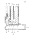
- FIG. 2 is a side sectional view of the lower end portion of the liquid crystal panel module 10.
- the left side indicates the front side of the liquid crystal panel module 10
- the right side indicates the rear side of the liquid crystal panel module 10.
- the liquid crystal panel module 10 includes a light source device 40, a light guide plate 70, a reflection sheet 75, a heat radiating plate 80, a backlight chassis 90, and an optical sheet 100.
- the light source device 40, the light guide plate 70, the reflection sheet 75, the heat radiating plate 80, and the backlight chassis 90 constitute a backlight of the liquid crystal panel module 10.
- the backlight of the liquid crystal panel module 10 employs an edge light system in which the light source device 40 is disposed to face one side surface of the light guide plate 70.
- the liquid crystal panel module 10 includes an inner frame 35.
- the inner frame 35 is a synthetic resin frame that covers the side periphery of the backlight and the optical sheet 100.
- the frame 30 covers the liquid crystal panel 20 and the side periphery of the inner frame 35 from the outside of the inner frame 35 and the outside of the screen 21 on the front surface of the liquid crystal panel 20.
- the light source device 40 is a component that emits light to one lower side surface of the light guide plate 70.
- the light source device 40 includes an LED (Light Emitting Diode) package 50 and an LED substrate 60.
- the LED package 50 is a small piece in which a light source is sealed with a translucent resin.
- the LED substrate 60 is a rectangular aluminum plate extending in the left-right direction.
- the plurality of LED packages 50 are mounted on the LED substrate 60 in a state of being arranged in the longitudinal direction of the LED substrate 60.
- the light guide plate 70 is a rectangular flat plate, and is made of, for example, acrylic or polycarbonate.
- the reflection sheet 75 is a thin film made of a synthetic resin having a substantially rectangular shape and high reflectivity.
- the size of the reflection sheet 75 is substantially the same as the size of the rear surface of the light guide plate 70 and is attached to the rear surface of the light guide plate 70.
- the reflection sheet 75 reflects the light to the front side in order to effectively use the light traveling backward in the light guide plate 70.
- the heat sink 80 is a rectangular plate member made of, for example, iron or aluminum.
- the long side of the heat sink 80 is substantially parallel to the longitudinal direction of the LED substrate 60.
- the reflection sheet 75 is spaced from the front side of the heat dissipation plate 80 via a spacer. In addition, the reflection sheet 75 may contact
- the heat radiating plate 80 includes a bent portion 81 bent to the front side at a lower end portion thereof, and has an L shape in a side sectional view.
- the LED substrate 60 on which the LED package 50 is mounted is attached to the upper surface of the bent portion 81 with, for example, a double-sided tape.
- the heat radiating plate 80 has a function of releasing heat generated from the light source device 40 to the outside of the liquid crystal panel module 10.
- the backlight chassis 90 is a rectangular parallelepiped box that holds the light guide plate 70, the reflection sheet 75, the heat dissipation plate 80, and the optical sheet 100.
- the backlight chassis 90 is made of, for example, iron or aluminum. Note that the heat sink 80 may also function as the backlight chassis 90.
- the optical sheet 100 is a substantially rectangular thin film.
- the size of the optical sheet 100 is substantially the same as the size of the light guide plate 70 and the liquid crystal panel 20.
- the optical sheet 100 includes, for example, a diffusion sheet, a prism sheet, and a viewing angle widening sheet.
- the diffusion sheet diffuses light.
- the prism sheet has a plurality of lenses arranged adjacent to each other and controls the traveling direction of light.
- the viewing angle expansion sheet expands the range of viewing angles so that good display performance can be obtained.
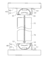
- FIG. 3 is a top view of the LED package 50.
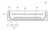
- 4 is a cross-sectional view of the LED package 50 taken along the line IV-IV in FIG.
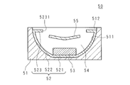
- FIG. 5 is a cross-sectional view of the LED package 50 taken along the line VV in FIG.
- the LED package 50 has a rectangular parallelepiped shape extending in the left-right direction.
- the LED package 50 includes a frame 51, a container 52, an LED 53, a translucent resin 54, and a reflection plate 55.
- the frame 51 is a rectangular parallelepiped box extending in the left-right direction, and is made of ceramics or resin.
- a boat bottom-shaped recess 511 is provided inside the frame 51.
- the upper surface of the frame 51 is opened in a rectangular shape, and constitutes a frame opening 512.
- the container 52 is a copper reflector placed on the recess 511 of the frame 51 such that the recess 511 of the frame 51 is used as a mold.
- the container 52 has a boat bottom shape extending in the left-right direction.
- the inner surface of the container 52 is silver-plated.
- the container 52 may be made of white ceramics having a high reflectance.
- the container 52 includes a bottom wall 521, a reflective side wall 522, and a reflective top wall 523.
- the bottom wall 521 is a rectangular flat plate portion extending in the left-right direction.
- one LED 53 as the light source is mounted on the inner surface of the bottom wall 521.
- the reflection side wall 522 is a wall extending from the entire peripheral edge of the bottom wall 521 so as to extend upward along the inner surface of the frame 51.
- the upper end of the reflection side wall 522 is positioned below the frame opening 512 of the frame 51.
- the reflection side wall 522 has an arc shape or an elliptic arc shape that curves in a convex shape toward the outside.
- each of the reflection ceiling walls 523 protrudes from the front tip portion and the rear tip portion of the reflection side wall 522 to the inner peripheral side.
- the two reflective ceiling walls 523 are provided in a substantially vertical direction with respect to the reflective sidewall 522 from the front end portions of the front and rear reflective sidewalls 522 extending in the left-right direction. ing.
- the reflective ceiling wall 523 resembles a roof that is half-opened at a covered dome venue.
- the reflection ceiling wall 523 has a function of reflecting light from the LED 53 toward the inside of the container 52.
- the reflective ceiling wall 523 may be provided in a frame shape on the inner peripheral side along the distal end portion of the reflective side wall 522.
- the region on the inner peripheral side from the tip ends of the two reflecting ceiling walls 523 constitutes a rectangular opening 5231.
- the area of the opening 5231 is narrower than the frame opening 512 by the area of the reflective ceiling wall 523.
- the translucent resin 54 is a silicon resin, an epoxy resin, an acrylic resin, a norbornene resin or the like having a high light transmittance.
- the translucent resin 54 is filled in the container 52.
- the translucent resin 54 is also filled in the space from the opening 5231 to the frame opening 512.
- the reflection plate 55 is a copper plate having a tray shape recessed inward (lower side), and extends in the left-right direction.
- the reflecting plate 55 is sealed with a translucent resin 54 at a position near the opening 5231 between the center point of the opening 5231 of the container 52 and the LED 53.
- the reflecting plate 55 may be sealed with the translucent resin 54 at the center point of the opening 5231 or a position slightly above the center point of the opening 5231.
- the translucent resin 54 that fills the space above the opening 5231 may be omitted.
- the reflector 55 may be made of white ceramics having a high reflectance.
- the reflection plate 55 reflects light from the outside of the container 52 to the outside of the container 52 and reflects light from the inside of the container 52 to the inside of the container 52. More specifically, the reflecting plate 55 reflects the light emitted from the light guide plate 70 to the light source device 40 (returned light) to the light guide plate 70, the light from the LED 53 and the LED 53 reflected by the inner surface of the container 52.
- the light has a function of reflecting light from the inside of the container 52.
- the reflecting plate 55 Since the reflecting plate 55 is disposed near the center of the opening 5231 of the container 52, a gap is formed between the tip of the reflecting ceiling wall 523 and the peripheral portion of the reflecting plate 55. Light resulting from the LED 53 is emitted from the gap toward one side of the light guide plate 70.
- FIG. 6 is an explanatory diagram showing a state in which light from the LED 53 is reflected by the reflection ceiling wall 523.
- a broken line including an arrow indicates a light path from the LED 53.
- Light from the LED 53 is emitted to the top surface side of the container 52 at various angles.
- the light emitted at a larger angle with respect to the normal direction of the LED substrate 60 leaks into the space outside the one side surface of the light guide plate 70.
- the light leaking into the space outside the one side surface of the light guide plate 70 is not used for displaying an image on the liquid crystal panel 20. Therefore, the luminance on the screen 21 is reduced by the amount of light leaking to the space outside the one side surface of the light guide plate 70.
- the reflection ceiling wall 523 is provided at a position where the light emitted from the LED 53 to an angle outside the one side surface of the light guide plate 70 reaches. Therefore, the light emitted from the LED 53 to an angle outside the one side surface of the light guide plate 70 is reflected by the reflective ceiling wall 523 and irradiates the reflective side wall 522 of the container 52. The light that irradiates the reflective sidewall 522 of the container 52 is reflected by the inner surface of the reflective sidewall 522.
- FIG. 7 is an explanatory view showing a state in which the light of the LED 53 reflected by the inner surface of the container 52 and the lower surface of the reflecting plate 55 enters the light guide plate 70.
- a broken line including an arrow indicates a light path from the LED 53.
- ⁇ represents an angle at which light is totally reflected on the inner surface of the light guide plate 70.
- the light guide plate 70 is made of acrylic, for example, ⁇ ⁇ 42 degrees.
- a part of the light reflected by the reflecting ceiling wall 523 and reflected by the inner surface of the reflecting side wall 522 is guided through the gap formed between the tip of the reflecting ceiling wall 523 and the peripheral portion of the reflecting plate 55. Is emitted toward one side. That is, the light emitted from the LED 53 to an angle outside the one side surface of the light guide plate 70 is recycled for image display on the liquid crystal panel 20. Further, part of the light reflected by the inner surface of the reflecting side wall 522 is repeatedly reflected by the lower surface of the reflecting plate 55 and the inner surface of the container 52, and finally the tip of the reflecting ceiling wall 523 and the peripheral portion of the reflecting plate 55 The light is emitted toward one side surface of the light guide plate 70 from the gap formed between the two.
- the light finally reflected by the reflective side wall 522 becomes outgoing light that passes through a gap formed between the tip of the reflective ceiling wall 523 and the peripheral portion of the reflective plate 55.
- the incident angle of the light to the light guide plate 70 is determined so that the emitted light is totally reflected by the inner surface of the light guide plate 70. Then, the incident angle of light to the light guide plate 70 is adjusted at the position of the focal point corresponding to the inner surface of the reflection side wall 522.
- the position of the focal point depends on the shape or curvature of the inner surface of the reflection side wall 522 having a circular sectional shape or an elliptical arc shape in the side sectional view (an elliptical arc where the focal point exists is desirable, but the circular arc is not approximately different).
- the incident angle of light on the light guide plate 70 corresponds to the inner surface shape of the reflective sidewall 522. Since the container 52 has a shape extending in the left-right direction (perpendicular to the paper surface of FIG. 7), the focal point passes through the center of the light guide plate 70 and is substantially the same as one surface of the light guide plate 70 that irradiates the liquid crystal panel 20 with light. Located on parallel planes.
- FIG. 8 is an explanatory view showing convergent light emitted from the LED package 50.
- the hatched portion shows convergent light.
- the line segment to which the arrow was added to both ends has shown the fluctuation
- the light from the LED 53 is reflected by the reflective ceiling wall 523, the reflective sidewall 522, and the reflective plate 55 of the container 52, and finally formed between the tip of the reflective ceiling wall 523 and the peripheral portion of the reflective plate 55.
- the light flux that passes through the gap is converged. Even if the light guide plate 70 before thermal expansion is farthest from the light source device 40, the incident angle of the convergent light on the light guide plate 70 is adjusted so that all of the convergent light is incident on one side surface of the light guide plate 70. Therefore, the shape of the inner surface of the reflection side wall 522 is adjusted.
- the width of the convergent light is also related.
- the width of the convergent light varies depending on the shape of the inner surface of the reflective side wall 522.
- the width of the convergent light varies depending on the size and position of the reflecting ceiling wall 523 and the reflecting plate 55. Therefore, in order to adjust the width of the convergent light to the light guide plate 70 so that all the convergent light is incident on one side surface of the light guide plate 70, the shape of the inner surface of the reflective side wall 522, the reflective ceiling wall 523, and the reflector 55 The size and position are adjusted.
- FIG. 9 is an explanatory diagram showing that the convergent light emitted from the LED package 50 is narrowed.
- the hatched portion indicates convergent light.
- the line segment between the arrows indicates an example of the incident light spot diameter.
- the incident light spot diameter is the width of convergent light that is narrowed down and incident on one side surface of the light guide plate 70.
- the light incident spot diameter can be changed by adjusting the shape of the inner surface of the reflection side wall 522 and the size and position of the reflection ceiling wall 523 and the reflection plate 55. If the incident light spot diameter is set to the size shown in FIG. 9, the thickness of the light guide plate 70 can be reduced to the length of the line segment sandwiched between the arrows. Thereby, the manufacturing cost of the light-guide plate 70 can be reduced. Further, reducing the thickness of the light guide plate 70 contributes to the thinning of the liquid crystal panel module 10.
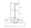
- FIG. 10 is an explanatory diagram illustrating a state in which the reflection plate 55 reflects the return light from the light guide plate 70 to the light guide plate 70.
- the return light includes the light that is emitted from the LED package 50 reflected by one side of the light guide plate 70 and returned to the LED package 50, and the light that is emitted from the LED package 50 is the inner surface of the light guide plate 70. And light returning to the LED package 50.
- the reflection plate 55 reflects the return light from the light guide plate 70 to the light guide plate 70. Thus, the return light again enters the light guide plate 70 and is recycled for image display by the liquid crystal panel 20.
- the LED package 50 includes the frame 51. However, the LED package 50 may not include the frame 51. If there is a concern about the strength of the container 52 by not using the frame 51, the thickness of the container 52 may be increased.
- the LED package 50 includes the reflection plate 55. However, the LED package 50 may not include the reflection plate 55. Since the LED package 50 includes at least the reflective ceiling wall 523, the light that has leaked to the outside of the light guide plate 70 in the related art is recycled and applied to one side of the light guide plate 70. Thereby, the incident efficiency of the light source device 40 with respect to the light guide plate 70 is improved as compared with the prior art.
- the incident efficiency with respect to an optical member like the light guide plate 70 can be improved.
- the reflection ceiling wall 523 reflects the light emitted from the LED 53 at an angle toward the outside of the light guide plate 70 to the inside of the container 52.
- the light reflected into the container 52 is finally emitted to one side surface of the light guide plate 70.
- the light source device 40 can improve the incident efficiency with respect to the light guide plate 70.
- the reflection plate 55 reflects the return light from the light guide plate 70 to the light guide plate 70. Further, the reflection plate 55 reflects the light from the LED 53 to the inside of the container 52. The light reflected into the container 52 is finally emitted to one side surface of the light guide plate 70. Thereby, the light source device 40 can improve the incident efficiency with respect to the light guide plate 70.
- the light from the LED 53 is made uniform while being reflected by the inner surface of the container 52 and the lower surface of the reflecting plate 55. Therefore, the backlight can reduce luminance unevenness on the screen 21 of the liquid crystal panel 20.
- the light immediately after entering the light guide plate 70 from the light source device 40 is totally reflected on the inner surface of the light guide plate 70 by adjusting the incident angle of the light to the light guide plate 70 in consideration of the thermal expansion of the light guide plate 70. Can do. Thereby, the light guide plate 70 can irradiate uniform light from the one surface to the rear surface of the liquid crystal panel 20.
- the light guide plate 70 of the backlight is changed to a thinner one by adjusting the shape of the inner surface of the reflection side wall 522 and the size and position of the reflection ceiling wall 523 and the reflection plate 55 to reduce the incident light spot diameter. Can do. Thereby, the manufacturing cost of the light-guide plate 70 can be reduced.
- FIG. 11 is an explanatory diagram showing a state in which the two light source devices 40 are arranged opposite to one side surface and the other side surface of the light guide plate 70, respectively.
- one light source device 40 is drawn one by one so as to be opposed to the upper side surface and the lower side surface of the light guide plate 70.
- Each light source device 40 emits light to the upper side surface and the lower side surface of the light guide plate 70.
- the light emitted from the light source device 40 arranged to face the upper side surface of the light guide plate 70 is represented by one hatched arrow.
- the backlight includes two light source devices 40, so that the rear surface of the liquid crystal panel 20 can be irradiated with strong light. Thereby, the brightness
- the light emitted from one light source device 40 to the light guide plate 70 passes through the light guide plate 70 and reaches the other light source device 40.
- the light that has reached the other light source device 40 is reflected by, for example, the reflection plate 55 of the other light source device 40 and re-emitted to the light guide plate 70.
- the light that has reached the other light source device 40 is incident on the inside of the container 52 through a gap formed between, for example, the tip of the reflective ceiling wall 523 of the other light source device 40 and the peripheral portion of the reflecting plate 55.
- the light is re-emitted from the gap to the light guide plate 70.
- the backlight can recycle and use the light passing through the light source device 40 that passes through the light guide plate 70.
- FIG. 12 is an explanatory diagram showing a state in which light incident on the light guide plate 70 from the light source device 40 is reflected on the other side surface of the light guide plate 70.
- light that is incident on the light guide plate 70 from the light source device 40 and is reflected on the other side surface is represented by one hatched arrow.
- the reflective sheet 76 is affixed on the other side opposite to one side of the light guide plate 70 facing the light source device 40.
- the reflection sheet 76 is a thin film made of a synthetic resin having a high reflectance.
- the reflection sheet 76 is incident on the light guide plate 70 from the light source device 40 and reflects the light that has reached the reflection sheet 76.
- the light reflected by the reflection sheet 76 passes through the light guide plate 70 and returns to the optical device 40.
- the light returning to the optical device 40 is re-emitted to the light guide plate 70 in the same manner as in the first modification. Accordingly, the backlight can be recycled without leaking the light of the optical device 40 that has reached the other side of the light guide plate 70 to the outside of the light guide plate 70.
- Embodiment 2 relates to a form in which a prism pattern is formed on the surface of the translucent resin 54 of the LED package 50 facing one side surface of the light guide plate 70.
- the same components as those in the first embodiment are denoted by the same reference numerals, and detailed description thereof is omitted.
- the liquid crystal panel 20 includes a liquid crystal and two polarizing filters before and after the liquid crystal.
- the front polarizing filter allows only S-polarized light to pass, and the rear polarizing filter allows only P-polarized light to pass.
- the backlight irradiates only the P-polarized light corresponding to the total light amount of the S-polarized light rather than irradiating the liquid crystal panel 20 with both the S-polarized light and the P-polarized light.
- the luminance of the screen 21 of the liquid crystal panel 20 can be increased by this amount. Therefore, a prism pattern that transmits P-polarized light and reflects part of S-polarized light is formed on the surface of the translucent resin 54 of the LED package 50. A part of the reflected S-polarized light is reflected by the container 52 and the reflection plate 55 of the LED package 50 and recycled, and then re-emitted to the light guide plate 70.
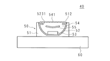
- FIG. 13 is a side sectional view of the light source device 40.
- a plurality of inverted V-shaped prisms 541 are formed on the surface of the translucent resin 54 filled from the opening 5231 to the frame opening 512.
- the plurality of prisms 541 extend substantially in parallel in the left-right direction, for example. Thereby, a prism pattern including a plurality of substantially parallel prisms 541 is formed on the surface of the translucent resin 54.
- the prism pattern is not limited to a large number of linear prisms 541 arranged in parallel.
- the prism pattern may be formed by concentrically molding a plurality of prisms having similar shapes with different sizes (for example, prisms having a rectangular frame shape).
- the prism pattern may be composed of one spiral prism.
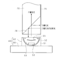
- FIG. 14 is an explanatory diagram showing the behavior of P-polarized light and S-polarized light on the surface of the translucent resin 54.
- the prism 541 shown in FIG. 14 is a right angle prism, for example.
- the light reaching the surface of the prism 541 includes P-polarized light and S-polarized light.
- the prism 541 allows the P-polarized light to pass therethrough.
- the prism 541 reflects the S-polarized light twice and returns it to the LED package 50 for recycling as light.
- the prism 541 refracts S-polarized light inward, thereby condensing the light guide plate 70 and increasing the light used for displaying an image. A small amount of light spreads out by reflection / refraction and becomes a loss.
- a prism pattern was formed on the surface of the translucent resin 54.
- an optical film having a prism pattern formed on the surface of the translucent resin 54 may be attached.
- the brightness of the screen 21 of the liquid crystal panel 20 can be increased.
- the light source device 40 converts part of the S-polarized light that has reached the surface of the prism 541 at the total reflection angle into P-polarized light and emits it to the light guide plate 70. Accordingly, a part of the S-polarized light that is originally blocked by the polarizing filter of the liquid crystal panel 20 is converted into P-polarized light and used for image display on the liquid crystal panel 20, so that the screen of the liquid crystal panel 20 is correspondingly increased.
- the brightness of 21 increases.
- Embodiment 3 relates to a configuration in which a polarizing beam splitter (polarizing beam splitter) is attached to one end portion on one side of the light guide plate 70 where light is incident from the light source device 40.
- the polarization beam splitter is an optical component that separates incident light into P-polarized light and S-polarized light at a constant separation ratio.
- the same components as those in the first and second embodiments are denoted by the same reference numerals, and detailed description thereof is omitted.
- FIG. 15 is an explanatory view showing the light source device 40 and the light guide plate 70 to which the polarization beam splitter 78 is attached.
- a broken line including an arrow indicates a light path from the light source device 40 in the light guide plate 70 and the polarization beam splitter 78.
- the polarization beam splitter 78 has a right-angle prism shape.
- the oblique side surface of the polarizing beam splitter 78 is attached to a cut surface of the light guide plate 70 that is obliquely cut so that one end portion is inclined from the rear side to the front side and from the inner side to the outer side. Therefore, the light from the light source device 40 enters one side surface of the polarization beam splitter 78.
- the reflection sheet 75 is attached to the rear surface of the light guide plate 70 and the rear surface of the polarization beam splitter 78 across the joint between the light guide plate 70 and the polarization beam splitter 78.
- the light emitted from the light source device 40 enters the polarization beam splitter 78 and reaches the boundary surface between the polarization beam splitter 78 and the light guide plate 70.
- Incident light is separated into P-polarized light and S-polarized light.
- the separated P-polarized light passes through the boundary surface between the polarization beam splitter 78 and the light guide plate 70 and enters the light guide plate 70 as it is.
- the separated S-polarized light is reflected backward (laterally) at the boundary surface between the polarizing beam splitter 78 and the light guide plate 70.
- the S-polarized light reflected backward is further reflected forward by the reflection sheet 75.
- the S-polarized light reflected forward is reflected downward at the boundary surface between the polarization beam splitter 78 and the light guide plate 70 and returns to the light source device 40.
- the S-polarized light that has returned to the light source device 40 is reflected by the upper surface of the reflecting plate 55, the inner surface of the container 52, and the lower surface of the reflecting plate 55, and enters the polarizing beam splitter 78.
- the P-polarized light converted when the S-polarized light push-back is repeated enters the polarization beam splitter 78, passes through the boundary surface between the polarization beam splitter 78 and the light guide plate 70, and enters the light guide plate 70.
- the luminance of the screen 21 of the liquid crystal panel 20 can be increased.
- a polarizing beam splitter 78 that transmits only P-polarized light is attached to the lower end portion of the light guide plate 70 facing the light source device 40.
- the separated S-polarized light is returned to the light source device 40 for recycling.
- the container 52 includes the bottom wall 521 and the bottom wall 521.
- a reflection side wall 522 that is provided around the inner surface and bulges outward, reflects light from the light source 53, and protrudes from an edge on the top surface side of the reflection side wall 522 to the inner peripheral side;
- a reflection ceiling wall 523 having an opening for reflecting the light from the light source 53 to the inside and emitting the reflected light is characterized.
- the incident efficiency with respect to an optical member like the light guide plate 70 can be improved.
- the reflective ceiling 523 reflects the light emitted from the light source 53 at an angle toward the outside of the optical member to the inside of the container 52.
- the light reflected to the inside of the container 52 is finally emitted to the optical member.
- the light source device 40 can improve the incident efficiency with respect to an optical member.
- the light source device 40 fills the inside of the container 52 and covers the outside of the container 52, and is smaller than the opening 5231 of the reflective ceiling wall 523, and near the center of the opening 5231. And a reflective plate 55 which is sealed with a light-sensitive resin 54 and reflects light from inside and outside of the container 52.
- the incident efficiency with respect to an optical member like the light guide plate 70 can be improved.
- the reflection plate 55 reflects the return light from the optical member to the optical member.
- the reflection plate 55 reflects light from the light source 53 toward the inside of the container 52.
- the light reflected to the inside of the container 52 is finally emitted to the optical member.
- the light source device 40 can improve the incident efficiency with respect to an optical member.
- the light source device 40 is characterized in that one or a plurality of prisms 541 are formed on the surface of the translucent resin 54 through which the light emitted from the opening 5231 of the reflective ceiling wall 523 passes.
- the light source device 40 According to the light source device 40, power consumption can be reduced. Since the light source device 40 has the prism 541 that transmits only the P-polarized light on the surface of the translucent resin 54, the S-polarized light is converted into P-polarized light in advance. As a result, the light source device 40 can secure a sufficient amount of light with a smaller number of light sources 53 than in the case where the S-polarized light after emission is not used, thereby reducing power consumption.
- the illumination device includes the light source device 40 described above, and a light guide plate 70 that faces one side of the light source device 40 and diffuses light from the light source device 40 incident on the inside from the one side surface and emits the light from the one surface.
- the light guide plate 70 separates light incident from the light source device 40 into P-polarized light and S-polarized light at one end including the one side surface, and passes the P-polarized light.
- a polarized light separating element 78 that reflects polarized light to the outside of the light guide plate is provided.
- a polarizing beam splitter 78 that transmits only P-polarized light is attached to the lower end portion of the light guide plate 70 facing the light source device 40.
- the separated S-polarized light is returned to the light source device 40 for recycling.
- the liquid crystal display device 210 includes the illumination device described above and the liquid crystal panel 20 that displays an image using light emitted from one surface of the light guide plate 70 of the illumination device.
- the brightness of the screen 21 of the liquid crystal panel 20 can be improved.
- the reflective ceiling 523 reflects light emitted from the light source 53 at an angle toward the outside of the light guide plate 70 to the inside of the container 52.
- the light reflected into the container 52 is finally emitted to one side surface of the light guide plate 70.
- the light source device 40 is characterized in that the container 52 has a shape extending in one direction, and the cross-sectional view of the reflective side wall 522 has an arc shape or an elliptical arc shape.
- the reflection side wall 522 has an arc shape or an elliptic arc shape that curves outwardly.
- the focal point corresponding to the inner surface of the reflective side wall 522 passes through the center of the light guide plate 70 and is located on a surface substantially parallel to one surface of the light guide plate 70 that irradiates the liquid crystal panel 20 with light.
- the shape of the inner surface of the reflective side wall 522 and the size and position of the reflective top wall 523 and the reflective plate 55 are adjusted.
- the incident light spot diameter can be made equal to or smaller than the width of one side surface of the light guide plate 70.
- the light source device 40 is characterized in that the reflection plate 523 has a tray shape recessed inward.
- the reflection plate 523 Since the reflection plate 523 has a basin shape recessed inward, the return light from the light guide plate 70 can be reflected only to the inside of the light guide plate 70 and is not leaked to the outside of the light guide plate 70.
- the light source device 40 includes a rectangular parallelepiped frame 51 that houses the container 52.
- Storing the container 52 in the rectangular parallelepiped frame 51 can increase the strength of the light source device 40 and facilitate the attachment of the light source device 40 to other devices.
- the illuminating device is characterized in that a reflection sheet 76 for reflecting light transmitted to the outside to the inside is attached to the other side surface of the light guide plate 70 facing the one side surface.
- the illumination device can be recycled without leaking the light of the optical device 40 that has reached the other side of the light guide plate 70 to the outside of the light guide plate 70.
- the illuminating device includes two light source devices 40, and the light source devices 40 are arranged to face each other on one side surface of the light guide plate 70 and the other side surface facing the one side surface.
- the illuminating device can irradiate the rear surface of the liquid crystal panel 20 with strong light by including two light source devices 40. Thereby, the illuminating device can improve the brightness of the screen 21 of the liquid crystal panel 20.
- the polarized light separating element 78 is a right angle prism having an oblique side surface that is inclined from the inner side to the outer side of the light guide plate 70 with respect to the direction from the other surface of the light guide plate to the entire surface.
- a reflection sheet 75 that reflects the light emitted to the outside is affixed to the other surface of the light guide plate 70 including 78.
- the S-polarized light can be recycled to the irradiation light to the liquid crystal panel 20.
- the P-polarized light separated by the polarized light separating element 78 forming a right-angle prism passes through the oblique side surface of the right-angle prism.
- the separated S-polarized light is reflected to the other surface side inside the light guide plate 70 by the oblique side surface of the right-angle prism.
- the S-polarized light reflected to the other surface side of the light guide plate 70 is reflected by the reflection sheet 75 and reflected to the light source device 40 by the oblique side surface of the right-angle prism.
- the S-polarized light returning to the light source device 40 is converted into P-polarized light and reenters the polarized light separation element 78.
- the illuminating device can irradiate the rear surface of the liquid crystal panel 20 with the P-polarized light by recycling the S-polarized light.
Landscapes
- Physics & Mathematics (AREA)
- General Physics & Mathematics (AREA)
- Optics & Photonics (AREA)
- Planar Illumination Modules (AREA)
Abstract
光学部材に対する入射効率を向上させることができる光源装置、照明装置及び液晶表示装置を提供する。 容器52の内底面に実装された光源53からの光を該容器52の天面側に出射する光源装置40において、前記容器52は、底壁521と、該底壁521に周設され、内面が外側に膨出し、前記光源53からの光を反射する反射側壁522と、該反射側壁522における天面側の縁部から内周側へ張り出すように突設され、前記光源53からの光を内部に反射し、反射した光を出射するための開口5231を有する反射天壁523とを有する。
Description
本願は、光源装置、照明装置及び液晶表示装置に関する。
光源からの光を一定範囲の角度へ出射する光源装置がある(例えば、特許文献1参照)。特許文献1に係る光源装置は、光源に電流を供給する平板状の導体部が光源に対して光の出射側と反対側に配置され、導体部表面には高反射率を有する銀メッキ層が形成されている。特許文献1に係る光源装置は、銀メッキ層が光源からの光を反射することにより、発光効率を高めている。特許文献1に係る光源装置は、液晶表示装置の直下型及びエッジ型のバックライトに利用することができる。
ところで、エッジ型バックライトを利用する液晶表示装置では、導光板の熱膨張を考慮して、当該導光板の一側面から一定距離離隔して光源装置が配置される。そのため、特許文献1に係る光源装置の光を導光板のような光学部材に出射する場合、光源装置と光学部材との間の距離に応じて、光学部材の外側に出射される光がある。従って、特許文献1に係る光源装置が出射する光量に対して光学部材に入射する光量の入射効率は十分とはいえない。なお、光学部材には、他に照明用の拡散板等がある。
本願は、かかる事情に鑑みてなされたものである。その目的は、光学部材に対する入射効率を向上させることができる光源装置、照明装置及び液晶表示装置を提供することにある。
本願に係る光源装置は、容器の内底面に実装された光源からの光を該容器の天面側に出射する光源装置において、前記容器は、底壁と、該底壁に周設され、内面が外側に膨出し、前記光源からの光を反射する反射側壁と、該反射側壁における天面側の縁部から内周側へ張り出すように突設され、前記光源からの光を内部に反射し、反射した光を出射するための開口を有する反射天壁とを有することを特徴とする。
本願に係る光源装置は、前記容器の内部に充填され、かつ該容器の外部を覆う透光性樹脂と、前記反射天壁の開口よりも小さく、該開口中央付近にて前記透光性樹脂に封止され、前記容器内外からの光を反射する反射板とを備えることを特徴とする。
本願に係る光源装置は、前記反射天壁の開口から出射された光が通過する前記透光性樹脂の表面に、一又は複数のプリズムが形成されていることを特徴とする。
本願に係る照明装置は、上記に記載の光源装置と、該光源装置に一側面が対向され、該一側面から内部に入射した該光源装置からの光を拡散して一面から出射する導光板とを備え、該導光板は、前記一側面が含まれる一端部に、前記光源装置から入射した光をP偏光光及びS偏光光に分離し、該P偏光光を通過させ、該S偏光光を該導光板の外部へ反射する偏光光分離素子を有することを特徴とする。
本願に係る液晶表示装置は、上記に記載の照明装置と、該照明装置の導光板の一面から出射された光を用いて画像を表示する液晶パネルとを備えることを特徴とする。
本願に係る光源装置等によれば、光学部材に対する入射効率を向上させることができる。
本願に係る一実施例の液晶表示装置は、テレビジョン受信機、電子黒板、チューナに接続して使用される表示装置、デスクトップ型コンピュータに接続して使用される表示装置及びデジタルサイネージに利用される表示装置を含む。また、本願に係る一実施例の液晶表示装置は、タブレット型コンピュータ、PDA(Personal Digital Assistant)及び携帯電話に利用される表示装置を含む。以下では、液晶表示装置の一例として、液晶パネル及びバックライト(照明装置)を含む液晶パネルモジュールを実施の形態に関する図面に基づいて説明する。
実施の形態1
図1は、液晶パネルモジュール10を正面側からみた斜視図である。ここで、起立姿勢の液晶パネルモジュール10が画像を表示する画面21に対して視聴者が正対した場合、画面21から視聴者側を前側又は正面側、その反対を後側又は背面側とする。液晶パネルモジュール10及び画面21は、横長の矩形状をなす。視聴者から画面21に向かって、画面21の長辺方向右側を液晶パネルモジュール10の右側、画面21の長辺方向左側を液晶パネルモジュール10の左側とする。画面21の短辺方向上側を液晶パネルモジュール10の上側、画面21の短辺方向下側を液晶パネルモジュール10の下側とする。
図1は、液晶パネルモジュール10を正面側からみた斜視図である。ここで、起立姿勢の液晶パネルモジュール10が画像を表示する画面21に対して視聴者が正対した場合、画面21から視聴者側を前側又は正面側、その反対を後側又は背面側とする。液晶パネルモジュール10及び画面21は、横長の矩形状をなす。視聴者から画面21に向かって、画面21の長辺方向右側を液晶パネルモジュール10の右側、画面21の長辺方向左側を液晶パネルモジュール10の左側とする。画面21の短辺方向上側を液晶パネルモジュール10の上側、画面21の短辺方向下側を液晶パネルモジュール10の下側とする。
液晶パネルモジュール10は、液晶パネル20及び枠体30を含む。
液晶パネル20は、前側に画面21を有し、画面21に画像を表示する。
枠体30は、合成樹脂又はアルミニウムからなる上枠、2本の側枠及び下枠を含み、これらが合体した場合の前面視形状は、矩形枠状をなす。
液晶パネル20は、前側に画面21を有し、画面21に画像を表示する。
枠体30は、合成樹脂又はアルミニウムからなる上枠、2本の側枠及び下枠を含み、これらが合体した場合の前面視形状は、矩形枠状をなす。
図2は、液晶パネルモジュール10下端部の側断面図である。図2において、左側は液晶パネルモジュール10の前側を、右側は液晶パネルモジュール10の後側を示す。
液晶パネルモジュール10は、光源装置40、導光板70、反射シート75、放熱板80、バックライトシャーシ90及び光学シート100を含む。光源装置40、導光板70、反射シート75、放熱板80及びバックライトシャーシ90は、液晶パネルモジュール10のバックライトを構成している。液晶パネルモジュール10のバックライトは、光源装置40が導光板70の一側面に対向配置されたエッジライト方式を採用している。
液晶パネルモジュール10は、光源装置40、導光板70、反射シート75、放熱板80、バックライトシャーシ90及び光学シート100を含む。光源装置40、導光板70、反射シート75、放熱板80及びバックライトシャーシ90は、液晶パネルモジュール10のバックライトを構成している。液晶パネルモジュール10のバックライトは、光源装置40が導光板70の一側面に対向配置されたエッジライト方式を採用している。
液晶パネルモジュール10は、内枠35を含む。内枠35は、バックライトと、光学シート100との側周を覆う合成樹脂製の枠体である。枠体30は、内枠35の外側から液晶パネル20及び内枠35の側周並びに液晶パネル20前面の画面21の外側を覆っている。
光源装置40は、導光板70における下側の一側面に光を出射する構成部である。光源装置40は、LED(Light Emitting Diode)パッケージ50及びLED基板60を含む。LEDパッケージ50は、光源が透光性樹脂で封止された小片である。LED基板60は、左右方向に延びた矩形状のアルミニウム板である。複数のLEDパッケージ50は、LED基板60の長手方向に配列した状態で、LED基板60上に搭載されている。
導光板70は、矩形状の平板であり、例えばアクリル、ポリカーボネイトからなる。
反射シート75は、略矩形をなし、高反射率を有する合成樹脂からなる薄膜である。反射シート75の大きさは、導光板70の後面の大きさと略同一であり、導光板70の後面に貼付される。反射シート75は、導光板70内にて後側に進行する光を有効利用するために、当該光を前側に反射する。
反射シート75は、略矩形をなし、高反射率を有する合成樹脂からなる薄膜である。反射シート75の大きさは、導光板70の後面の大きさと略同一であり、導光板70の後面に貼付される。反射シート75は、導光板70内にて後側に進行する光を有効利用するために、当該光を前側に反射する。
放熱板80は、例えば鉄又はアルミニウムからなる矩形板状部材である。放熱板80の長辺は、LED基板60の長手方向と略平行である。反射シート75は、放熱板80の前側にスペーサを介して離隔配置されている。なお、反射シート75は、スペーサを介さずに、放熱板80の前面と当接していてもよい。
放熱板80は、その下端部に前側に曲折された曲成部81を含み、側断面視L字状をなす。LEDパッケージ50を搭載するLED基板60は、曲成部81の上面に例えば両面テープで貼設されている。放熱板80は、光源装置40からの発熱を液晶パネルモジュール10の外部へ放出する機能を有している。
バックライトシャーシ90は、導光板70、反射シート75、放熱板80及び光学シート100を保持する直方体状の箱体である。バックライトシャーシ90は、例えば鉄又はアルミニウムからなる。
なお、放熱板80がバックライトシャーシ90の機能を兼ねてもよい。
なお、放熱板80がバックライトシャーシ90の機能を兼ねてもよい。
光学シート100は、略矩形の薄膜である。光学シート100の大きさは、導光板70及び液晶パネル20の大きさと略同一である。光学シート100は、例えば拡散シート、プリズムシート及び視野角拡大シートを含む。拡散シートは、光を拡散する。プリズムシートは、隣接して配列された複数のレンズを有し、光の進行方向を制御する。視野角拡大シートは、良好な表示性能が得られるように、視角の範囲を拡大する。
図3は、LEDパッケージ50の上面図である。
図4は、LEDパッケージ50の図3におけるIV-IV線の断面図である。
図5は、LEDパッケージ50の図3におけるV-V線の断面図である。
図4は、LEDパッケージ50の図3におけるIV-IV線の断面図である。
図5は、LEDパッケージ50の図3におけるV-V線の断面図である。
LEDパッケージ50は、左右方向に延びた直方体状をなす。LEDパッケージ50は、フレーム51、容器52、LED53、透光性樹脂54及び反射板55を含む。
フレーム51は、左右方向に延びた直方体状をなす箱体であり、セラミクス又は樹脂からなる。フレーム51の内部には、舟底形状の凹部511が設けられている。フレーム51の上面は、矩形状に開口しており、フレーム開口512を構成している。
容器52は、フレーム51の凹部511を型枠とするように、フレーム51の凹部511に載置される銅製のリフレクターである。容器52は、左右方向に延びた舟底形状をなす。容器52の内面には、銀メッキが施されている。なお、容器52は、高反射率を有する白色セラミクスで作成されてもよい。
容器52は、底壁521、反射側壁522及び反射天壁523を含む。
底壁521は、左右方向に延びた矩形状の平板部である。光源のLED53は、例えば1個であり、底壁521の内面に搭載されている。
底壁521は、左右方向に延びた矩形状の平板部である。光源のLED53は、例えば1個であり、底壁521の内面に搭載されている。
反射側壁522は、底壁521の全周縁部からフレーム51の内面に沿って上側に延びるように延設された壁である。反射側壁522の上端はフレーム51のフレーム開口512よりも下方に位置する。図5の断面では、反射側壁522は、外側へ向かって凸状に湾曲した円弧状又は楕円弧状をなす。
反射天壁523は、2つであり、夫々反射側壁522の前側先端部及び後側先端部から内周側へ張り出すように突設されている。図3及び図5に示すように、2つの反射天壁523は、夫々左右方向に延びた前側及び後側の反射側壁522部分の先端部から、反射側壁522に対して略垂直方向に設けられている。LEDパッケージ50において、反射天壁523は、屋根付きドーム会場での半開き状態になった屋根に似ている。反射天壁523は、LED53からの光を容器52内部へ反射する機能を有している。
なお、反射天壁523は、反射側壁522の先端部に沿って内周側に額縁状に周設されてもよい。
なお、反射天壁523は、反射側壁522の先端部に沿って内周側に額縁状に周設されてもよい。
2つの反射天壁523の各先端部よりも内周側の領域は、矩形状の開口5231を構成している。開口5231の面積は、反射天壁523の面積の分だけ、フレーム開口512より狭い。
透光性樹脂54は、光透過率が高いシリコン系樹脂、エポキシ系樹脂、アクリル系樹脂、ノルボルネン系樹脂等である。透光性樹脂54は、容器52の内部に充填されている。また、透光性樹脂54は、開口5231からフレーム開口512までの空間にも充填されている。
反射板55は、内側(下側)に窪んだ盆状をなす銅製の板であり、左右方向に延びている。図5において、反射板55は、容器52の開口5231の中心点とLED53との間であって、開口5231寄りの位置で透光性樹脂54に封止されている。なお、反射板55は開口5231の中心点又は開口5231の中心点より若干上方の位置で透光性樹脂54に封止されてもよい。
なお、反射板55が図5における位置で透光性樹脂54に封止される場合、開口5231より上側の空間に充填される透光性樹脂54はなくてもよい。
なお、反射板55が図5における位置で透光性樹脂54に封止される場合、開口5231より上側の空間に充填される透光性樹脂54はなくてもよい。
反射板55の上面及び下面には、銀メッキが施されている。なお、反射板55は、高反射率を有する白色セラミクスで作成されてもよい。
反射板55は、容器52外部からの光を容器52外部へ反射し、容器52内部からの光を容器52内部へ反射する。より詳細には、反射板55は、導光板70が光源装置40に出射した光(戻した光)を導光板70に反射する機能と、LED53からの光及び容器52の内面で反射されたLED53からの光を容器52内部に反射する機能とを有している。反射板55は容器52の開口5231の中心付近に配置しているため、反射天壁523の先端部と、反射板55の周部との間に隙間が形成されている。LED53に起因する光は、当該隙間から導光板70の一側面へ向かって出射される。
反射板55は、容器52外部からの光を容器52外部へ反射し、容器52内部からの光を容器52内部へ反射する。より詳細には、反射板55は、導光板70が光源装置40に出射した光(戻した光)を導光板70に反射する機能と、LED53からの光及び容器52の内面で反射されたLED53からの光を容器52内部に反射する機能とを有している。反射板55は容器52の開口5231の中心付近に配置しているため、反射天壁523の先端部と、反射板55の周部との間に隙間が形成されている。LED53に起因する光は、当該隙間から導光板70の一側面へ向かって出射される。
次に、液晶パネルモジュール10のバックライトの動作について説明する。
図6は、LED53からの光が反射天壁523で反射される様子を示す説明図である。図6において、矢印を含む折れ線は、LED53からの光の経路を示している。LED53からの光は、様々な角度で容器52の天面側へ出射される。
図6は、LED53からの光が反射天壁523で反射される様子を示す説明図である。図6において、矢印を含む折れ線は、LED53からの光の経路を示している。LED53からの光は、様々な角度で容器52の天面側へ出射される。
仮に反射天壁523がない場合、LED基板60の法線方向に対してより大きな角度で出射される光ほど、導光板70の一側面よりも外側の空間へ漏れる。導光板70の一側面より外側の空間へ漏れる光は、液晶パネル20での画像の表示に使用されない。そのため、画面21における輝度は、導光板70の一側面よりも外側の空間へ漏れる光の分だけ低下する。
反射天壁523は、LED53から導光板70の一側面よりも外側の角度へ出射された光が到達する位置に設けられている。そのため、LED53から導光板70の一側面より外側の角度へ出射された光は、反射天壁523で反射されて、容器52の反射側壁522を照射する。容器52の反射側壁522を照射する光は、反射側壁522内面で反射される。
図7は、容器52の内面及び反射板55の下面で反射されたLED53の光が導光板70に入射する様子を示す説明図である。図7において、矢印を含む折れ線は、LED53からの光の経路を示している。図7において、θは、導光板70の内面で光が全反射する角度を示している。導光板70が例えばアクリルからなる場合、θ≧42度である。
反射天壁523で反射され、かつ反射側壁522内面で反射された光の一部は、反射天壁523の先端部と、反射板55の周部との間に形成される隙間から導光板70の一側面へ向かって出射される。すなわち、LED53から導光板70の一側面よりも外側の角度へ出射された光は、液晶パネル20での画像表示にリサイクル使用される。また、反射側壁522内面で反射された光の一部は、反射板55の下面及び容器52の内面で繰り返し反射され、最終的に反射天壁523の先端部と、反射板55の周部との間に形成される隙間から導光板70の一側面へ向かって出射される。
最終的に反射側壁522で反射された光が、反射天壁523の先端部と、反射板55の周部との間に形成される隙間を通過する出射光となる。この出射光が導光板70の内面で全反射するように、導光板70への光の入射角度が決定される。そして、導光板70への光の入射角度は、反射側壁522の内面に対応する焦点の位置で調整される。焦点の位置は、側断面視形状が円弧状又は楕円弧状をなす反射側壁522内面の形状又は曲率に依存する(焦点が存在する楕円弧が望ましいが、円弧でも近似的に差はつかない)。すなわち、導光板70への光の入射角度は、反射側壁522の内面形状に対応する。
容器52は左右方向(図7の紙面に対する垂直方向)に延びた形状をなしているので、焦点は導光板70の中心を通過し、液晶パネル20に光を照射する導光板70の一面と略平行な面上に位置する。
容器52は左右方向(図7の紙面に対する垂直方向)に延びた形状をなしているので、焦点は導光板70の中心を通過し、液晶パネル20に光を照射する導光板70の一面と略平行な面上に位置する。
図8は、LEDパッケージ50から出射された収束光を示す説明図である。図8において、ハッチングを施した部分は、収束光を示している。また、図8において、両端に矢印が付加された線分は、熱膨張及び熱収縮による導光板70の一側面位置の変動を示している。
LED53からの光は、容器52の反射天壁523、反射側壁522及び反射板55で反射されて、最終的に反射天壁523の先端部と、反射板55の周部との間に形成される隙間を通過する光束に収束される。熱膨張前の導光板70が光源装置40から最も離れた位置にあっても、収束光の全てが導光板70の一側面に入射するように、導光板70への収束光の入射角度を調整すべく、反射側壁522内面の形状は調整されている。
導光板70が光源装置40から最も離れた位置にある場合であっても、収束光の全てが導光板70の一側面に入射するためには、収束光の幅も関係する。収束光の幅は、反射側壁522内面の形状によって変化する。また、収束光の幅は、反射天壁523及び反射板55の大きさと位置とによって変化する。そのため、収束光の全てが導光板70の一側面に入射するように、導光板70への収束光の幅を調整すべく、反射側壁522内面の形状と、反射天壁523並びに反射板55の大きさ及び位置とは調整されている。
図9は、LEDパッケージ50から出射された収束光が絞られていることを示す説明図である。図9において、ハッチングを施した部分は、収束光を示している。また、図9において、矢印で挟まれた線分は、入光スポット径の一例を示している。入光スポット径は、絞り込まれて導光板70の一側面に入射する収束光の幅である。
反射側壁522内面の形状と、反射天壁523並びに反射板55の大きさ及び位置とを調整することにより、入光スポット径を変化させることができる。仮に、入光スポット径を図9の大きさにした場合、導光板70の厚さを、矢印で挟んだ線分の長さまで薄くすることができる。これにより、導光板70の製造コストを低減することができる。また、導光板70の厚さを薄くすることは、液晶パネルモジュール10の薄化に資する。
図10は、反射板55が導光板70からの戻り光を導光板70へ反射する様子を示す説明図である。ここでの戻り光は、LEDパッケージ50から出射された光が導光板70の一側面で反射されてLEDパッケージ50へ戻ってくる光と、LEDパッケージ50から出射された光が導光板70の内面で拡散されてLEDパッケージ50へ戻ってくる光とを含む。
反射板55は、導光板70からの戻り光を導光板70へ反射する。これにより、戻り光は再び導光板70に入射して、液晶パネル20による画像表示にリサイクル使用される。
反射板55は、導光板70からの戻り光を導光板70へ反射する。これにより、戻り光は再び導光板70に入射して、液晶パネル20による画像表示にリサイクル使用される。
上述では、LEDパッケージ50は、フレーム51を含んでいた。しかし、LEDパッケージ50は、フレーム51を含まなくてもよい。フレーム51を用いないことにより、容器52の強度が懸念される場合、容器52の厚さをより厚くすればよい。
上述では、LEDパッケージ50は、反射板55を含んでいた。しかし、LEDパッケージ50は、反射板55を含まなくてもよい。LEDパッケージ50は、少なくとも反射天壁523を含むため、従来導光板70の外側へ漏れていた光をリサイクルして導光板70の一側面に照射する。これにより、導光板70に対する光源装置40の入射効率は、従来よりも向上する。
光源装置40によれば、導光板70のような光学部材に対する入射効率を向上させることができる。
反射天壁523は、導光板70の外側へ向かう角度でLED53が出射する光を容器52の内部へ反射する。容器52の内部へ反射された光は、最終的に導光板70の一側面に出射される。これにより、光源装置40は、導光板70に対する入射効率を向上させることができる。
反射天壁523は、導光板70の外側へ向かう角度でLED53が出射する光を容器52の内部へ反射する。容器52の内部へ反射された光は、最終的に導光板70の一側面に出射される。これにより、光源装置40は、導光板70に対する入射効率を向上させることができる。
反射板55は、導光板70からの戻り光を導光板70に反射する。また、反射板55は、LED53からの光を容器52の内部へ反射する。容器52の内部へ反射された光は、最終的に導光板70の一側面に出射される。これにより、光源装置40は、導光板70に対する入射効率を向上させることができる。
LED53からの光は、容器52の内面及び反射板55の下面で反射される間に均一化される。そのため、バックライトは、液晶パネル20の画面21における輝度ムラを低下させることができる。
導光板70の熱膨張を考慮して、導光板70への光の入射角度を調整することにより、光源装置40から導光板70へ入射した直後の光を導光板70の内面で全反射させることができる。これにより、導光板70は、その一面から液晶パネル20の後面へ均一な光を照射することができる。
反射側壁522内面の形状と、反射天壁523並びに反射板55の大きさ及び位置とを調整して、入光スポット径を小さくすることにより、バックライトの導光板70をより薄いものに変えることができる。これにより、導光板70の製造コストを低減することができる。
(変形例1)
図11は、2つの光源装置40を夫々導光板70の一側面と、他側面とに対向配置した様子を示す説明図である。図11では、導光板70の上側側面と、下側側面とに夫々対向配置された光源装置40が1つずつ描かれている。各光源装置40は、導光板70の上側側面と、下側側面とに光を出射する。図11では、導光板70の上側側面に対向配置された光源装置40から出射された光を、ハッチングを施した1本の矢印で代表させている。
図11は、2つの光源装置40を夫々導光板70の一側面と、他側面とに対向配置した様子を示す説明図である。図11では、導光板70の上側側面と、下側側面とに夫々対向配置された光源装置40が1つずつ描かれている。各光源装置40は、導光板70の上側側面と、下側側面とに光を出射する。図11では、導光板70の上側側面に対向配置された光源装置40から出射された光を、ハッチングを施した1本の矢印で代表させている。
バックライトは光源装置40を2つ備えることにより、液晶パネル20の後面により強い光を照射することができる。これにより、液晶パネル20の画面21の輝度を向上させることができる。
一の光源装置40から導光板70へ出射された光は、導光板70を通過し、他の光源装置40に到達する。他の光源装置40に到達した光は、例えば他の光源装置40の反射板55で反射されて、導光板70に再出射される。また、他の光源装置40に到達した光は、例えば他の光源装置40の反射天壁523の先端部と、反射板55の周部との間に形成される隙間から容器52の内部へ入射し、最終的に当該隙間から導光板70に再出射される。これにより、バックライトは、導光板70を通過する光源装置40の通過光をリサイクル使用することができる。
(変形例2)
図12は、光源装置40から導光板70に入射した光を、導光板70の他側面で反射する様子を示す説明図である。図12では、光源装置40から導光板70に入射し、他側面で反射された光を、ハッチングを施した1本の矢印で代表させている。
図12は、光源装置40から導光板70に入射した光を、導光板70の他側面で反射する様子を示す説明図である。図12では、光源装置40から導光板70に入射し、他側面で反射された光を、ハッチングを施した1本の矢印で代表させている。
光源装置40が対向配置する導光板70の一側面と反対側の他側面に、反射シート76が貼付されている。反射シート76は、高反射率を有する合成樹脂からなる薄膜である。反射シート76は、光源装置40から導光板70に入射し、反射シート76に到達した光を反射する。反射シート76で反射された光は、導光板70を通過して、光学装置40に戻ってくる。光学装置40に戻った光は、変形例1と同様にして、導光板70に再出射される。これにより、バックライトは、導光板70の他側面に達した光学装置40の光を導光板70の外部へ漏らすことなく、リサイクル使用することができる。
実施の形態2
実施の形態2は、導光板70の一側面と対向するLEDパッケージ50の透光性樹脂54の表面にプリズムパターンを成形する形態に関する。
実施の形態2において、実施の形態1と同様である構成要素には同一の参照番号を付してその詳細な説明を省略する。
実施の形態2は、導光板70の一側面と対向するLEDパッケージ50の透光性樹脂54の表面にプリズムパターンを成形する形態に関する。
実施の形態2において、実施の形態1と同様である構成要素には同一の参照番号を付してその詳細な説明を省略する。
液晶パネル20は、液晶と、液晶を挟む前後2枚の偏光フィルタを含む。前側の偏光フィルタはS偏光光のみを通過させ、後側の偏光フィルタはP偏光光のみを通過させる。液晶パネル20において、バックライトは液晶パネル20にS偏光光とP偏光光との両者を照射するよりも、両者の合計光量に対応するP偏光光のみを照射した方が、S偏光光のエネルギーの分だけ液晶パネル20の画面21の輝度を上昇させることができる。そこで、LEDパッケージ50の透光性樹脂54の表面にP偏光光を透過し、一部のS偏光光を反射するプリズムパターンを成形する。反射された一部のS偏光光は、LEDパッケージ50の容器52及び反射板55に反射されてリサイクルされ、導光板70に再出射される。
図13は、光源装置40の側断面図である。開口5231からフレーム開口512まで充填された透光性樹脂54の表面に、側断面視逆V字状のプリズム541が複数形成されている。複数のプリズム541は、例えば左右方向に略平行に延びている。これにより、透光性樹脂54の表面に、略平行な複数のプリズム541からなるプリズムパターンが成形されている。
なお、プリズムパターンは、多数の直線状プリズム541を略平行に並べたものに限らない。プリズムパターンは、大きさが異なる相似形状のプリズム(例えば、矩形枠状をなすプリズム)を同心状に複数成形したものでもよい。あるいは、プリズムパターンは、1つの螺旋状のプリズムから構成されてもよい。
図14は、透光性樹脂54の表面でのP偏光光及びS偏光光の振る舞いを示す説明図である。図14に示すプリズム541は、例えば直角プリズムである。プリズム541の表面に達した光には、P偏光光及びS偏光光が含まれている。プリズム541は、P偏光光を通過させる。他方、プリズム541は、S偏光光を2重反射させてLEDパッケージ50に戻り光としてリサイクルする。プリズム541は、屈折ではS偏光光を内側に屈折させることで、導光板70に対して集光を行い、画像の表示に使用する光を増やすことができる。わずかな光は、反射/屈折により外に広がり、損失になる。
上述では、透光性樹脂54の表面にプリズムパターンを成形した。しかし、透光性樹脂54の表面にプリズムパターンが成形された光学フィルムを貼付してもよい。
光源装置40によれば、液晶パネル20の画面21の輝度を上昇させることができる。
光源装置40は、全反射角度でプリズム541の表面に達したS偏光光の一部をP偏光光に変換して導光板70に出射する。従って、液晶パネル20の偏光フィルタによって本来遮断されるS偏光光の一部は、P偏光光に変換されて、液晶パネル20での画像表示に利用されるため、その分だけ液晶パネル20の画面21の輝度は上昇する。
光源装置40は、全反射角度でプリズム541の表面に達したS偏光光の一部をP偏光光に変換して導光板70に出射する。従って、液晶パネル20の偏光フィルタによって本来遮断されるS偏光光の一部は、P偏光光に変換されて、液晶パネル20での画像表示に利用されるため、その分だけ液晶パネル20の画面21の輝度は上昇する。
実施の形態3
実施の形態3は、光源装置40から光が入射される導光板70の一側面側の一端部に、偏光ビームスプリッタ(Polarizing Beam Splitter、偏光光分離素子)を取り付ける形態に関する。偏光ビームスプリッタは、入射光を一定の分離比でP偏光光とS偏光光とに分離する光学部品である。
実施の形態3において、実施の形態1、2と同様である構成要素には同一の参照番号を付してその詳細な説明を省略する。
実施の形態3は、光源装置40から光が入射される導光板70の一側面側の一端部に、偏光ビームスプリッタ(Polarizing Beam Splitter、偏光光分離素子)を取り付ける形態に関する。偏光ビームスプリッタは、入射光を一定の分離比でP偏光光とS偏光光とに分離する光学部品である。
実施の形態3において、実施の形態1、2と同様である構成要素には同一の参照番号を付してその詳細な説明を省略する。
図15は、光源装置40と、偏光ビームスプリッタ78が取り付けられた導光板70とを示す説明図である。矢印を含む折れ線は、導光板70内及び偏光ビームスプリッタ78内における光源装置40からの光の経路を示している。
偏光ビームスプリッタ78は、直角プリズム状をなす。偏光ビームスプリッタ78の斜側面は、一端部が後側から前側へ、かつ内側から外側へ傾斜するように斜めに切断された導光板70の切断面に、貼付されている。そのため、光源装置40からの光は、偏光ビームスプリッタ78の一側面に入射する。反射シート75は、導光板70及び偏光ビームスプリッタ78の継ぎ目を跨いで、導光板70の後面と、偏光ビームスプリッタ78の後面とに貼付されている。
光源装置40から出射された光は、偏光ビームスプリッタ78に入射し、偏光ビームスプリッタ78と導光板70との境界面に到達する。入射光は、P偏光光と、S偏光光とに分離される。分離されたP偏光光は、偏光ビームスプリッタ78と導光板70との境界面を通過し、そのまま導光板70内に入射する。他方、分離されたS偏光光は、偏光ビームスプリッタ78と導光板70との境界面で後方(横)へ反射される。後方へ反射されたS偏光光は、更に反射シート75により前方へ反射される。前方へ反射されたS偏光光は、偏光ビームスプリッタ78と導光板70との境界面で下方へ反射されて、光源装置40に戻る。
光源装置40に戻ったS偏光光は、反射板55の上面並びに容器52の内面及び反射板55の下面で反射されて、偏光ビームスプリッタ78に入射される。このS偏光光押し戻しを繰り返す際に変換されたP偏光光が、偏光ビームスプリッタ78に入射し、偏光ビームスプリッタ78と導光板70との境界面を通過して導光板70内に入射する。
液晶パネルモジュール10のバックライトによれば、液晶パネル20の画面21の輝度を上昇させることができる。
P偏光光のみを透過する偏光ビームスプリッタ78が、光源装置40と対向する導光板70の下端部に貼付されている。分離されたS偏光光は、光源装置40に戻されてリサイクル使用される。これにより、光源装置40は、より少ないLED53で十分な画面21の輝度を確保することができるので、消費電力を削減することができる。
P偏光光のみを透過する偏光ビームスプリッタ78が、光源装置40と対向する導光板70の下端部に貼付されている。分離されたS偏光光は、光源装置40に戻されてリサイクル使用される。これにより、光源装置40は、より少ないLED53で十分な画面21の輝度を確保することができるので、消費電力を削減することができる。
開示された実施の形態は、全ての点で例示であって制限的なものではないと考えられるべきである。本発明の範囲は上述の説明ではなくて請求の範囲によって示され、請求の範囲と均等の意味及び範囲内での全ての変更が含まれることが意図される。
実施の形態で記載されている技術的特徴(構成要件)は、お互いに組合せ可能であり、組み合わせすることにより、新しい技術的特徴を形成することができる。
光源装置40は、容器52の内底面に実装された光源53からの光を該容器52の天面側に出射する光源装置40において、前記容器52は、底壁521と、該底壁521に周設され、内面が外側に膨出し、前記光源53からの光を反射する反射側壁522と、該反射側壁522における天面側の縁部から内周側へ張り出すように突設され、前記光源53からの光を内部に反射し、反射した光を出射するための開口を有する反射天壁523とを有することを特徴とする。
光源装置40によれば、導光板70のような光学部材に対する入射効率を向上させることができる。
反射天壁523は、光学部材の外側へ向かう角度で光源53が出射する光を容器52の内部へ反射する。容器52の内部へ反射された光は、最終的に光学部材に出射される。これにより、光源装置40は、光学部材に対する入射効率を向上させることができる。
反射天壁523は、光学部材の外側へ向かう角度で光源53が出射する光を容器52の内部へ反射する。容器52の内部へ反射された光は、最終的に光学部材に出射される。これにより、光源装置40は、光学部材に対する入射効率を向上させることができる。
光源装置40は、前記容器52の内部に充填され、かつ該容器52の外部を覆う透光性樹脂54と、前記反射天壁523の開口5231よりも小さく、該開口5231中央付近にて前記透光性樹脂54に封止され、前記容器52内外からの光を反射する反射板55とを備えることを特徴とする。
光源装置40によれば、導光板70のような光学部材に対する入射効率を向上させることができる。
反射板55は、光学部材からの戻り光を光学部材に反射する。また、反射板55は、光源53からの光を容器52の内部へ反射する。容器52の内部へ反射された光は、最終的に光学部材に出射される。これにより、光源装置40は、光学部材に対する入射効率を向上させることができる。
反射板55は、光学部材からの戻り光を光学部材に反射する。また、反射板55は、光源53からの光を容器52の内部へ反射する。容器52の内部へ反射された光は、最終的に光学部材に出射される。これにより、光源装置40は、光学部材に対する入射効率を向上させることができる。
光源装置40は、前記反射天壁523の開口5231から出射された光が通過する前記透光性樹脂54の表面に、一又は複数のプリズム541が形成されていることを特徴とする。
光源装置40によれば、消費電力を削減することができる。
光源装置40は、P偏光光のみを透過するプリズム541を透光性樹脂54の表面に有しているため、S偏光光を予めP偏光光に変換する。これにより、光源装置40は、出射後のS偏光光が利用されない場合よりも少ない光源53で十分な光量を確保することができるので、消費電力を削減することができる。
光源装置40は、P偏光光のみを透過するプリズム541を透光性樹脂54の表面に有しているため、S偏光光を予めP偏光光に変換する。これにより、光源装置40は、出射後のS偏光光が利用されない場合よりも少ない光源53で十分な光量を確保することができるので、消費電力を削減することができる。
照明装置は、上記に記載の光源装置40と、該光源装置40に一側面が対向され、該一側面から内部に入射した該光源装置40からの光を拡散して一面から出射する導光板70とを備え、該導光板70は、前記一側面が含まれる一端部に、前記光源装置40から入射した光をP偏光光及びS偏光光に分離し、該P偏光光を通過させ、該S偏光光を該導光板の外部へ反射する偏光光分離素子78を有することを特徴とする。
照明装置によれば、消費電力を削減することができる。
P偏光光のみを透過する偏光ビームスプリッタ78が、光源装置40と対向する導光板70の下端部に貼付されている。分離されたS偏光光は、光源装置40に戻されてリサイクル使用される。これにより、照明装置は、より少ないLED53で十分な画面21の輝度を確保することができるので、消費電力を削減することができる。
P偏光光のみを透過する偏光ビームスプリッタ78が、光源装置40と対向する導光板70の下端部に貼付されている。分離されたS偏光光は、光源装置40に戻されてリサイクル使用される。これにより、照明装置は、より少ないLED53で十分な画面21の輝度を確保することができるので、消費電力を削減することができる。
液晶表示装置210は、上記に記載の照明装置と、該照明装置の導光板70の一面から出射された光を用いて画像を表示する液晶パネル20とを備えることを特徴とする。
液晶表示装置210によれば、液晶パネル20の画面21の輝度を向上させることができる。
反射天壁523は、導光板70の外側へ向かう角度で光源53が出射する光を容器52の内部へ反射する。容器52の内部へ反射された光は、最終的に導光板70の一側面に出射される。これにより、光源装置40は、導光板70に対する入射効率を向上させるため、導光板70から液晶パネル20に照射される光の量が増大し、画面21の輝度が向上する。
反射天壁523は、導光板70の外側へ向かう角度で光源53が出射する光を容器52の内部へ反射する。容器52の内部へ反射された光は、最終的に導光板70の一側面に出射される。これにより、光源装置40は、導光板70に対する入射効率を向上させるため、導光板70から液晶パネル20に照射される光の量が増大し、画面21の輝度が向上する。
光源装置40は、前記容器52は一方向に延びた形状をなし、前記反射側壁522の該一方向視断面は円弧状又は楕円弧状をなすことを特徴とする。
反射側壁522は、外側へ向かって凸状に湾曲した円弧状又は楕円弧状をなす。反射側壁522の内面に対応する焦点は、導光板70の中心を通過し、液晶パネル20に光を照射する導光板70の一面と略平行な面上に位置する。反射側壁522の内面形状と、反射天壁523及び反射板55の大きさと位置とを調整することにより、入光スポット径を小さくすることができ、照明装置に含まれる導光板70をより薄いものに変えることができる。これにより、導光板70の製造コストを低減することができる。
熱膨張前の導光板70が光源装置40から最も隔離した位置にある場合であっても、反射側壁522内面の形状と、反射天壁523並びに反射板55の大きさ及び位置とを調整することにより、入光スポット径を導光板70の一側面の幅以下にすることができる。これにより、導光板70が熱膨張及び熱収縮により光源装置40との距離を変動させても、光源装置40は導光板70の外側に光を出射しない。
また、反射側壁522の形状を調整することにより、導光板70に対して焦点の位置を近づけたり遠ざけたりすることができるため、導光板70への入射角度を、導光板70内で全反射が起こる角度に調整することができる。
熱膨張前の導光板70が光源装置40から最も隔離した位置にある場合であっても、反射側壁522内面の形状と、反射天壁523並びに反射板55の大きさ及び位置とを調整することにより、入光スポット径を導光板70の一側面の幅以下にすることができる。これにより、導光板70が熱膨張及び熱収縮により光源装置40との距離を変動させても、光源装置40は導光板70の外側に光を出射しない。
また、反射側壁522の形状を調整することにより、導光板70に対して焦点の位置を近づけたり遠ざけたりすることができるため、導光板70への入射角度を、導光板70内で全反射が起こる角度に調整することができる。
光源装置40は、前記反射板523は内側に窪んだ盆状をなすことを特徴とする。
反射板523は、内側に窪んだ盆状をなすため、導光板70からの戻り光を導光板70の内側のみに反射することができ、導光板70の外側へ漏らさない。
光源装置40は、前記容器52を収納する直方体状のフレーム51を備えることを特徴とする。
容器52を直方体状のフレーム51に収納することで、光源装置40の強度を増大させ、かつ他の装置への光源装置40の取り付けを容易にすることができる。
照明装置は、前記一側面と対向する前記導光板70の他側面に、外部へ透過する光を内部に反射する反射シート76が貼付されていることを特徴とする。
照明装置は、導光板70の他側面に達した光学装置40の光を導光板70の外部へ漏らすことなく、リサイクル使用することができる。
照明装置は、前記光源装置40を二つ備え、前記導光板70の一側面及び該一側面と対向する他側面に夫々前記光源装置40が一つずつ対向配置されていることを特徴とする。
照明装置は、光源装置40を2つ備えることにより、液晶パネル20の後面により強い光を照射することができる。これにより、照明装置は、液晶パネル20の画面21の輝度を向上させることができる
照明装置は、前記偏光光分離素子78は前記導光板の他面から一面へ向かう方向に対して該導光板70の内側から外側へ傾斜する斜側面を有する直角プリズムであり、前記偏光光分離素子78を含む前記導光板70の他面に、外部へ出射される光を内部に反射する反射シート75が貼付されていることを特徴とする。
照明装置によれば、S偏光光を液晶パネル20への照射光にリサイクル使用することができる。
直角プリズムをなす偏光光分離素子78により分離されたP偏光光は、直角プリズムの斜側面を通過する。他方、分離されたS偏光光は、直角プリズムの斜側面により導光板70内部の他面側へ反射される。導光板70の他面側へ反射されたS偏光光は、反射シート75で反射され、直角プリズムの斜側面で光源装置40へ反射される。光源装置40へ戻ったS偏光光は、P偏光光に変換されて偏光光分離素子78に再入射する。これにより、照明装置は、S偏光光をリサイクル使用して、液晶パネル20の後面にP偏光光を照射することができる。
直角プリズムをなす偏光光分離素子78により分離されたP偏光光は、直角プリズムの斜側面を通過する。他方、分離されたS偏光光は、直角プリズムの斜側面により導光板70内部の他面側へ反射される。導光板70の他面側へ反射されたS偏光光は、反射シート75で反射され、直角プリズムの斜側面で光源装置40へ反射される。光源装置40へ戻ったS偏光光は、P偏光光に変換されて偏光光分離素子78に再入射する。これにより、照明装置は、S偏光光をリサイクル使用して、液晶パネル20の後面にP偏光光を照射することができる。
10 液晶パネルモジュール
20 液晶パネル
30 枠体
35 内枠
40 光源装置
50 LEDパッケージ
51 フレーム
511 凹部
512 フレーム開口
52 容器
521 底壁
522 反射側壁
523 反射天壁
5231 開口
53 LED(光源)
54 透光性樹脂
541 プリズム
55 反射板
60 LED基板
70 導光板
75 反射シート
76 反射シート
78 偏光ビームスプリッタ(偏光光分離素子)
80 放熱板
90 バックライトシャーシ
20 液晶パネル
30 枠体
35 内枠
40 光源装置
50 LEDパッケージ
51 フレーム
511 凹部
512 フレーム開口
52 容器
521 底壁
522 反射側壁
523 反射天壁
5231 開口
53 LED(光源)
54 透光性樹脂
541 プリズム
55 反射板
60 LED基板
70 導光板
75 反射シート
76 反射シート
78 偏光ビームスプリッタ(偏光光分離素子)
80 放熱板
90 バックライトシャーシ
Claims (5)
- 容器の内底面に実装された光源からの光を該容器の天面側に出射する光源装置において、
前記容器は、
底壁と、
該底壁に周設され、内面が外側に膨出し、前記光源からの光を反射する反射側壁と、
該反射側壁における天面側の縁部から内周側へ張り出すように突設され、前記光源からの光を内部に反射し、反射した光を出射するための開口を有する反射天壁と
を有する
ことを特徴とする光源装置。 - 前記容器の内部に充填され、かつ該容器の外部を覆う透光性樹脂と、
前記反射天壁の開口よりも小さく、該開口中央付近にて前記透光性樹脂に封止され、前記容器内外からの光を反射する反射板と
を備える
ことを特徴とする請求項1に記載の光源装置。 - 前記反射天壁の開口から出射された光が通過する前記透光性樹脂の表面に、一又は複数のプリズムが形成されている
ことを特徴とする請求項2に記載の光源装置。 - 請求項1から請求項3までのいずれか一項に記載の光源装置と、
該光源装置に一側面が対向され、該一側面から内部に入射した該光源装置からの光を拡散して一面から出射する導光板と
を備え、
該導光板は、前記一側面が含まれる一端部に、前記光源装置から入射した光をP偏光光及びS偏光光に分離し、該P偏光光を通過させ、該S偏光光を該導光板の外部へ反射する偏光光分離素子を有する
ことを特徴とする照明装置。 - 請求項4に記載の照明装置と、
該照明装置の導光板の一面から出射された光を用いて画像を表示する液晶パネルと
を備える
ことを特徴とする液晶表示装置。
Priority Applications (1)
| Application Number | Priority Date | Filing Date | Title |
|---|---|---|---|
| US14/908,277 US20160170126A1 (en) | 2013-07-30 | 2014-07-11 | Light Source Device, Lighting Device and Liquid Crystal Display Device |
Applications Claiming Priority (2)
| Application Number | Priority Date | Filing Date | Title |
|---|---|---|---|
| JP2013158084 | 2013-07-30 | ||
| JP2013-158084 | 2013-07-30 |
Publications (1)
| Publication Number | Publication Date |
|---|---|
| WO2015016048A1 true WO2015016048A1 (ja) | 2015-02-05 |
Family
ID=52431588
Family Applications (1)
| Application Number | Title | Priority Date | Filing Date |
|---|---|---|---|
| PCT/JP2014/068624 Ceased WO2015016048A1 (ja) | 2013-07-30 | 2014-07-11 | 光源装置、照明装置及び液晶表示装置 |
Country Status (2)
| Country | Link |
|---|---|
| US (1) | US20160170126A1 (ja) |
| WO (1) | WO2015016048A1 (ja) |
Cited By (3)
| Publication number | Priority date | Publication date | Assignee | Title |
|---|---|---|---|---|
| CN105047792A (zh) * | 2015-08-19 | 2015-11-11 | 无锡伊佩克科技有限公司 | 一种高发光效率的白光数码管封装结构 |
| JP2019114754A (ja) * | 2017-12-26 | 2019-07-11 | 京セラ株式会社 | 電子部品搭載用パッケージ、電子装置および電子モジュール |
| JP2021535544A (ja) * | 2018-08-13 | 2021-12-16 | レイア、インコーポレイテッドLeia Inc. | 光リサイクル光源を用いるグレーティングコリメータ、バックライトシステム、及び方法 |
Families Citing this family (2)
| Publication number | Priority date | Publication date | Assignee | Title |
|---|---|---|---|---|
| US9563002B2 (en) * | 2014-12-31 | 2017-02-07 | Shenzhen China Star Optoelectronics Technology Co., Ltd | Ultrathin planar light source apparatus |
| US11029564B1 (en) | 2019-12-19 | 2021-06-08 | Lumileds Llc | Polarizing edge coupled light in backlight |
Citations (7)
| Publication number | Priority date | Publication date | Assignee | Title |
|---|---|---|---|---|
| JPH09105933A (ja) * | 1995-10-13 | 1997-04-22 | Sekisui Chem Co Ltd | 面状発光装置 |
| JPH09152604A (ja) * | 1995-11-30 | 1997-06-10 | Sekisui Chem Co Ltd | 面状発光装置 |
| JP2006066657A (ja) * | 2004-08-27 | 2006-03-09 | Kyocera Corp | 発光装置および照明装置 |
| JP2006332638A (ja) * | 2005-04-28 | 2006-12-07 | Toyoda Gosei Co Ltd | Led装置 |
| JP2008270144A (ja) * | 2007-03-22 | 2008-11-06 | Furukawa Electric Co Ltd:The | ライトボックス |
| JP2011222574A (ja) * | 2010-04-05 | 2011-11-04 | Stanley Electric Co Ltd | 発光装置およびその製造方法 |
| JP2012134435A (ja) * | 2010-11-30 | 2012-07-12 | Mitsubishi Shindoh Co Ltd | バックライト用発光装置 |
Family Cites Families (5)
| Publication number | Priority date | Publication date | Assignee | Title |
|---|---|---|---|---|
| US6104454A (en) * | 1995-11-22 | 2000-08-15 | Hitachi, Ltd | Liquid crystal display |
| US6610598B2 (en) * | 2001-11-14 | 2003-08-26 | Solidlite Corporation | Surface-mounted devices of light-emitting diodes with small lens |
| DE102005030128B4 (de) * | 2004-06-28 | 2011-02-03 | Kyocera Corp. | Lichtemittierende Vorrichtung und Beleuchtungsvorrichtung |
| JP5084769B2 (ja) * | 2009-03-13 | 2012-11-28 | 株式会社ジャパンディスプレイイースト | 液晶表示装置 |
| TWI435030B (zh) * | 2011-05-06 | 2014-04-21 | 國立中央大學 | 高指向性光源裝置 |
-
2014
- 2014-07-11 US US14/908,277 patent/US20160170126A1/en not_active Abandoned
- 2014-07-11 WO PCT/JP2014/068624 patent/WO2015016048A1/ja not_active Ceased
Patent Citations (7)
| Publication number | Priority date | Publication date | Assignee | Title |
|---|---|---|---|---|
| JPH09105933A (ja) * | 1995-10-13 | 1997-04-22 | Sekisui Chem Co Ltd | 面状発光装置 |
| JPH09152604A (ja) * | 1995-11-30 | 1997-06-10 | Sekisui Chem Co Ltd | 面状発光装置 |
| JP2006066657A (ja) * | 2004-08-27 | 2006-03-09 | Kyocera Corp | 発光装置および照明装置 |
| JP2006332638A (ja) * | 2005-04-28 | 2006-12-07 | Toyoda Gosei Co Ltd | Led装置 |
| JP2008270144A (ja) * | 2007-03-22 | 2008-11-06 | Furukawa Electric Co Ltd:The | ライトボックス |
| JP2011222574A (ja) * | 2010-04-05 | 2011-11-04 | Stanley Electric Co Ltd | 発光装置およびその製造方法 |
| JP2012134435A (ja) * | 2010-11-30 | 2012-07-12 | Mitsubishi Shindoh Co Ltd | バックライト用発光装置 |
Cited By (5)
| Publication number | Priority date | Publication date | Assignee | Title |
|---|---|---|---|---|
| CN105047792A (zh) * | 2015-08-19 | 2015-11-11 | 无锡伊佩克科技有限公司 | 一种高发光效率的白光数码管封装结构 |
| JP2019114754A (ja) * | 2017-12-26 | 2019-07-11 | 京セラ株式会社 | 電子部品搭載用パッケージ、電子装置および電子モジュール |
| JP7021937B2 (ja) | 2017-12-26 | 2022-02-17 | 京セラ株式会社 | 電子部品搭載用パッケージ、電子装置および電子モジュール |
| JP2021535544A (ja) * | 2018-08-13 | 2021-12-16 | レイア、インコーポレイテッドLeia Inc. | 光リサイクル光源を用いるグレーティングコリメータ、バックライトシステム、及び方法 |
| JP7235850B2 (ja) | 2018-08-13 | 2023-03-08 | レイア、インコーポレイテッド | 光リサイクル光源を用いるグレーティングコリメータ、バックライトシステム、及び方法 |
Also Published As
| Publication number | Publication date |
|---|---|
| US20160170126A1 (en) | 2016-06-16 |
Similar Documents
| Publication | Publication Date | Title |
|---|---|---|
| CN101319759B (zh) | 发光器件、面光源装置和图像显示装置 | |
| US9354385B2 (en) | Curved display apparatus | |
| CN107461653B (zh) | 发光单元、显示器和照明装置 | |
| CN108121115B (zh) | 发光单元、显示器和照明设备 | |
| JP2012123995A (ja) | バックライト装置及びそれを用いた液晶表示装置 | |
| JP2006310221A (ja) | エッジ入力型バックライト及び液晶表示装置 | |
| TWI461797B (zh) | 背光模組 | |
| CN105339727B (zh) | 照明装置和液晶显示装置 | |
| CN108292008A (zh) | 导光板、面光源装置、显示装置以及电子设备 | |
| JP2012238431A (ja) | エッジライト型バックライトユニット及びこれを用いた液晶モジュール | |
| JPWO2011102033A1 (ja) | 面光源装置、および当該面光源装置を備えた液晶表示装置 | |
| KR102087965B1 (ko) | 백라이트 어셈블리 및 이를 포함하는 표시 장치 | |
| US20160170126A1 (en) | Light Source Device, Lighting Device and Liquid Crystal Display Device | |
| JP2013218125A (ja) | 液晶表示装置 | |
| JP6303972B2 (ja) | 面光源装置、表示装置、及び電子機器 | |
| KR101651888B1 (ko) | 백라이트 장치 | |
| JP2007048489A (ja) | バックライト装置 | |
| CN103105695A (zh) | 液晶面板组件和具有该液晶面板组件的图像显示装置 | |
| KR20160098921A (ko) | 백라이트 유닛 및 이를 포함하는 디스플레이 장치 | |
| JP7446065B2 (ja) | ディスプレイ装置 | |
| JP7249779B2 (ja) | 表示装置および電子機器 | |
| JP2009259653A (ja) | 線状光源及び面状ライトユニット並びに表示装置 | |
| JP6298986B2 (ja) | 照明装置 | |
| JP6708593B2 (ja) | 表示装置 | |
| JP2005235560A (ja) | 面状照明装置 |
Legal Events
| Date | Code | Title | Description |
|---|---|---|---|
| 121 | Ep: the epo has been informed by wipo that ep was designated in this application |
Ref document number: 14831731 Country of ref document: EP Kind code of ref document: A1 |
|
| WWE | Wipo information: entry into national phase |
Ref document number: 14908277 Country of ref document: US |
|
| NENP | Non-entry into the national phase |
Ref country code: DE |
|
| 122 | Ep: pct application non-entry in european phase |
Ref document number: 14831731 Country of ref document: EP Kind code of ref document: A1 |
|
| NENP | Non-entry into the national phase |
Ref country code: JP |