WO2014208294A1 - 静電容量型センサ - Google Patents
静電容量型センサ Download PDFInfo
- Publication number
- WO2014208294A1 WO2014208294A1 PCT/JP2014/064751 JP2014064751W WO2014208294A1 WO 2014208294 A1 WO2014208294 A1 WO 2014208294A1 JP 2014064751 W JP2014064751 W JP 2014064751W WO 2014208294 A1 WO2014208294 A1 WO 2014208294A1
- Authority
- WO
- WIPO (PCT)
- Prior art keywords
- back side
- electrode
- insulating
- insulating spacer
- front side
- Prior art date
- Legal status (The legal status is an assumption and is not a legal conclusion. Google has not performed a legal analysis and makes no representation as to the accuracy of the status listed.)
- Ceased
Links
Images


Classifications
-
- G—PHYSICS
- G01—MEASURING; TESTING
- G01L—MEASURING FORCE, STRESS, TORQUE, WORK, MECHANICAL POWER, MECHANICAL EFFICIENCY, OR FLUID PRESSURE
- G01L1/00—Measuring force or stress, in general
- G01L1/14—Measuring force or stress, in general by measuring variations in capacitance or inductance of electrical elements, e.g. by measuring variations of frequency of electrical oscillators
- G01L1/142—Measuring force or stress, in general by measuring variations in capacitance or inductance of electrical elements, e.g. by measuring variations of frequency of electrical oscillators using capacitors
- G01L1/148—Measuring force or stress, in general by measuring variations in capacitance or inductance of electrical elements, e.g. by measuring variations of frequency of electrical oscillators using capacitors using semiconductive material, e.g. silicon
-
- G—PHYSICS
- G01—MEASURING; TESTING
- G01G—WEIGHING
- G01G19/00—Weighing apparatus or methods adapted for special purposes not provided for in the preceding groups
- G01G19/44—Weighing apparatus or methods adapted for special purposes not provided for in the preceding groups for weighing persons
-
- G—PHYSICS
- G01—MEASURING; TESTING
- G01G—WEIGHING
- G01G19/00—Weighing apparatus or methods adapted for special purposes not provided for in the preceding groups
- G01G19/44—Weighing apparatus or methods adapted for special purposes not provided for in the preceding groups for weighing persons
- G01G19/445—Weighing apparatus or methods adapted for special purposes not provided for in the preceding groups for weighing persons in a horizontal position
Definitions
- the present invention relates to a capacitive sensor used as, for example, a load sensor or a touch sensor.
- the capacitance type sensor includes a plurality of front side electrodes, a plurality of back side electrodes, and a dielectric layer.
- the plurality of front electrodes are arranged on the front side of the dielectric layer.
- the plurality of backside electrodes are disposed on the backside of the dielectric layer.
- the plurality of front-side electrodes and the plurality of back-side electrodes are orthogonal to each other.
- a plurality of detection units are set in a portion where the plurality of front-side electrodes and the plurality of back-side electrodes overlap.
- the dielectric layer is compressed in the front and back direction. For this reason, the interelectrode distance between the front side electrode and back side electrode which comprises the said detection part becomes small. Therefore, the capacitance of the detection unit is increased.
- a load applied to the detection unit can be detected based on a change in capacitance accompanying a change in the distance between electrodes. Further, the load distribution in the surface direction of the capacitive sensor can be detected by detecting the load in the plurality of detection units. For this reason, an electrostatic capacitance type sensor is used, for example in bedclothes, such as a bed and a futon, when measuring the body pressure distribution of the person who is sleeping.
- An object of the present invention is to provide a capacitance type sensor that can suppress noise from the surroundings and that does not easily reduce detection accuracy.
- a capacitive sensor of the present invention includes a front side electrode part, a back side electrode part disposed on the back side of the front side electrode part, the front side electrode part, and the back side electrode part.
- a sensor part having a dielectric layer disposed between the insulating part, an insulating spacer disposed on at least one of the front side and the back side of the sensor part, and an earth that is disposed on the outer side in the front and back direction of the insulating spacer and is grounded
- An electrode and a control device that is electrically connected to the sensor unit, applies a voltage to the sensor unit, and transmits an electric quantity related to the capacitance of the sensor unit.
- the capacitive sensor of the present invention includes a ground electrode. For this reason, noise from peripheral devices can be suppressed.
- An insulating spacer is interposed between the ground electrode and the sensor unit. For this reason, the detection accuracy of the capacitive sensor is unlikely to decrease.
- the front electrode portion includes a plurality of front electrodes arranged in parallel with each other
- the back electrode portion includes a plurality of back electrodes arranged in parallel with each other
- the plurality of front side electrodes and the plurality of back side electrodes extend in directions intersecting each other, and when viewed from the front side or the back side, the plurality of front side electrodes and the plurality of back side electrodes It is better to have a configuration in which a plurality of detection units are set in a portion where and overlap.
- the load can be detected by a plurality of detection units. For this reason, the load distribution in the surface direction (direction orthogonal to the front and back directions) of the capacitive sensor can be detected.
- the insulating spacer is preferably composed of a plurality of insulating films laminated in the front and back directions. According to this configuration, the thickness of the insulating spacer in the front and back direction (that is, the distance between the ground electrode and the sensor unit) can be easily adjusted by changing the number of laminated insulating films.
- the insulating spacer includes a film connecting portion that partially connects the insulating films, and the insulating spacer includes a plurality of the insulating films formed by the film connecting portion. It is better to have a configuration including a constraining portion constrained to each other and a non-constraining portion in which the plurality of insulating films are not constrained to each other.
- the insulating spacer of the capacitive sensor with this configuration has a restraining portion. For this reason, it can control that a plurality of insulating films shift mutually.
- the insulating spacer of the capacitive sensor of this configuration includes an unconstrained portion. For this reason, it can suppress that a deformation
- the amount of expansion of the outer surface in the radius direction of curvature relative to the inner surface in the radius direction of curvature is smaller as the thickness in the front and back direction of the insulating film is smaller.
- the extension amount of the back surface with respect to the surface of the insulating film may be smaller as the thickness of the insulating film in the front-back direction is smaller.
- the insulating spacer is not composed of a single insulating film but is composed of a plurality of insulating films.
- the insulating spacer includes a non-restraining portion. For this reason, compared with the insulating spacer consisting of a single insulating film (the thickness of the insulating film in the front and back direction is the sum of the thicknesses of the front and back sides of the plurality of insulating films), the plurality of insulating films of the insulating spacer of this configuration Each is easy to bend. Therefore, the insulating spacer of this configuration is easily bent.
- the film connecting portion includes a corner connecting portion disposed at a corner of the insulating spacer when viewed from the front side or the back side, and the angle viewed from the front side or the back side. It is better to have a configuration including a central coupling portion disposed inside the partial coupling portion. According to this structure, a constraining part can be locally set to an insulating spacer by a corner
- the sensor unit is disposed on the back side of the surface of the bedding, and the central coupling unit is along the height direction of the sleeping person in the bedding, It is better to have an extended configuration.
- the film connecting portion preferably has a plurality of strip-like connecting portions arranged in a stripe shape when viewed from the front side or the back side.
- the band-shaped connecting portion can set the constraining portion in a striped manner on the insulating spacer.
- the sensor unit is disposed on the back side of the surface of the bedding, and the band-shaped connecting unit is along the height direction of a sleeping person in the bedding, It is better to have an extended configuration.
- the insulating film is preferably made of polyethylene.
- Polyethylene is inexpensive, has a low Young's modulus, and a low dielectric constant. For this reason, the insulating film of this structure has low manufacturing cost, is easy to bend, and has high insulation.
- one of the front electrode portion and the back electrode portion is an input electrode portion to which the voltage is applied from the control device.
- the other is an output side electrode part that transmits the amount of electricity to the control device, and the output side electrode part is arranged closer to the ground electrode than the input side electrode part. It is better to have a configuration.
- the earth electrode hardly affects the amount of electricity related to the capacitance of the sensor unit.
- a positioning hole penetrating the sensor portion, the insulating spacer, and the ground electrode in the front and back direction, the sensor portion, the insulating spacer, And a bag-like cover that accommodates the ground electrode, and the front and back layers of the cover are preferably joined on the radially inner side of the positioning hole.
- the sensor part, the insulating spacer, and the ground electrode inside the cover can be easily fixed and positioned with respect to the cover by joining both the front and back layers of the cover inside the positioning hole in the radial direction.
- the front and back layers of the cover are preferably welded. According to this configuration, both the front and back layers of the cover can be easily and firmly joined. Moreover, according to this structure, when joining a cover, another members, such as a clip, are unnecessary, for example. For this reason, when a person gets on the upper surface of the cover, riding comfort (for example, sitting comfort, sleeping comfort, etc.) is good.
- the present invention it is possible to provide a capacitive sensor that can suppress noise from the surroundings and that is difficult to reduce detection accuracy.
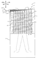
- FIG. 1 is a transparent top view of the capacitive sensor according to the first embodiment.
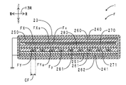
- FIG. 2 is a cross-sectional view in the II-II direction of FIG.
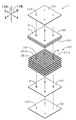
- FIG. 3 is an exploded perspective view of the capacitance type sensor.
- FIG. 4 is a block diagram of the capacitance type sensor.
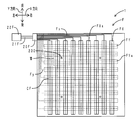
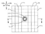
- FIG. 5 is a transparent top view of the capacitive sensor according to the second embodiment.
- FIG. 6 is an exploded perspective view of the capacitance type sensor.
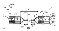
- FIG. 7 is an enlarged view in the frame VII of FIG. 8 is a cross-sectional view taken along the line VIII-VIII in FIG.
- the upper side corresponds to the “front side” of the present invention
- the lower side corresponds to the “back side” of the present invention
- the front-rear direction corresponds to the “height direction of a sleeping person in the bedding” of the present invention.
- FIG. 1 shows a transparent top view of the capacitive sensor of the present embodiment.
- FIG. 2 shows a cross-sectional view in the II-II direction of FIG.
- FIG. 3 shows an exploded perspective view of the capacitance type sensor.
- FIG. 4 shows a block diagram of the capacitance type sensor.
- the capacitive sensor 1 is laid under the bed sheet 9 of the bed.
- the capacitance type sensor 1 is based on the fact that the distance between the electrodes of the detection unit CF (distance between the front electrode unit FX and the back electrode unit FY), which will be described later, changes according to the weight of the sleeping person M.
- the body pressure distribution of the upper body of the person M is measured.
- another capacitive sensor (not shown) of the same type as the capacitive sensor 1 is disposed below the sheet 9.
- the capacitance type sensor measures the body pressure distribution of the lower body of the sleeping person M.
- the capacitive sensor 1 includes a sensor unit F, a connector 20F, a harness 21F, a control device 22F, a cover 23, a front side ground electrode 240, and a back side ground electrode 241.
- the front side ground electrode 240 and the back side ground electrode 241 are each included in the concept of the “ground electrode” of the present invention.
- the front-side insulating spacer 250 and the back-side insulating spacer 251 are each included in the concept of “insulating spacer” of the present invention.
- the front center connecting portion 291 and the rear center connecting portion 292 are each included in the concept of “center connecting portion” of the present invention.
- the cover 23 is made of a flexible soft urethane foam and has a bag shape.
- the cover 23 has an insulating property. Inside the cover 23, members other than the connector 20F, the harness 21F, and the control device 22F among the members constituting the capacitive sensor 1 are accommodated.
- the sensor part F includes a front side electrode part FX, nine front side wirings Fx, a back side electrode part FY, nine back side wirings Fy, a front side base material 260, a back side base material 261, and a front side cover coat 270.
- the rear cover coat 271, the dielectric layer 280, the reinforcing layer 281, and the detection unit CF are provided.
- the front side electrode portion FX corresponds to the “input side electrode portion” of the present invention.
- the back side electrode part FY corresponds to the “output side electrode part” of the present invention.
- the dielectric layer 280 is made of a flexible flexible urethane foam (specifically, PORON (registered trademark of Roger Sinoac Co., Ltd.)) and has a rectangular film shape.
- the dielectric layer 280 has an insulating property.
- the reinforcing layer 281 is disposed below the dielectric layer 280.
- the reinforcing layer 281 is made of PET (polyethylene terephthalate) and has a quadrangular film shape.
- the reinforcing layer 281 is harder (having a higher Young's modulus) than the dielectric layer 280.
- the reinforcing layer 281 has an insulating property.
- the front substrate 260 is disposed on the upper side of the dielectric layer 280.
- the front-side base material 260 is made of PET and has a quadrangular film shape.
- the front side base material 260 has insulating properties.
- the front-side wiring Fx is made of silver paste and has conductivity.
- the front-side wiring Fx electrically connects a later-described front-side electrode FXa and a later-described connector 20F.
- the front side electrode portion FX includes nine front side electrodes FXa.
- the front side electrode FXa is linear, and is screen-printed on the lower surface of the front side base material 260.
- the front electrode FXa extends in the front-rear direction (Y direction).
- the nine front electrodes FXa are arranged in the left-right direction (X direction).
- the front electrode FXa is made of carbon paste and has conductivity.
- the front side electrode FXa partially covers the front side wiring Fx from the lower side.
- the front side wiring Fx is disposed over the entire length in the longitudinal direction of the front side electrode FXa.
- the front cover coat 270 is made of polyester and has a quadrangular film shape.
- the front side cover coat 270 has an insulating property.
- the front side cover coat 270 is screen-printed on the lower surface of the front side base material 260.
- the front cover coat 270 covers nine front wirings Fx and nine front electrodes FXa from below.
- the back side substrate 261 is disposed below the reinforcing layer 281.
- the back side base material 261 is made of PET and has a quadrangular film shape.
- the back side base material 261 has an insulating property.
- the back side wiring Fy is made of silver paste and has conductivity.
- the back side wiring Fy electrically connects a back side electrode FYa described later and a connector 20F described later.
- the back side electrode part FY includes nine back side electrodes FYa.
- the back side electrode FYa is linear and is screen-printed on the upper surface of the back side base material 261.
- the back side electrode FYa extends in the left-right direction.
- the nine back electrodes FYa are arranged in the front-rear direction.
- the back electrode FYa is made of carbon paste and has conductivity.
- the back side electrode FYa partially covers the back side wiring Fy from above.
- the back side wiring Fy is disposed over the entire length in the longitudinal direction of the back side electrode FYa.
- the back side cover coat 271 is made of polyester and has a rectangular film shape.
- the back side cover coat 271 has insulating properties.
- the back side cover coat 271 is screen-printed on the upper surface of the back side base material 261.
- the back side cover coat 271 covers nine back side wirings Fy and nine back side electrodes FYa from above.
- Detector CF When viewed from above, the nine front electrodes FXa and the nine back electrodes FYa are arranged in a lattice pattern. A detection unit CF is set in a portion where the front side electrode FXa and the back side electrode FYa overlap. A total of 81 detectors CF are arranged.
- the front side insulating spacer 250 is disposed on the upper side of the front side base material 260.
- the front-side insulating spacer 250 is made of PE (polyethylene) and has a rectangular film shape.
- the front insulating spacer 250 has an insulating property.
- the front side ground wiring (not shown) made of silver paste is screen-printed on the entire top surface (surface on the outer side in the front and back direction) of the front side insulating spacer 250.
- the front-side ground electrode 240 is made of carbon paste and has a rectangular film shape.
- the front side ground electrode 240 has conductivity.
- the front side ground electrode 240 is entirely screen-printed on the upper surface of the front side ground wiring.
- the front side ground electrode 240 is electrically grounded via the front side ground wiring.
- the back side insulating spacer 251 is disposed below the back side base material 261. As shown in FIG. 3, the back-side insulating spacer 251 includes five insulating films 251a.
- the insulating film 251a is made of PE and has a quadrangular film shape.
- the insulating film 251a has insulating properties.
- the back end base material 262 is disposed below the back side insulating spacer 251.
- the back end base material 262 is made of PET and has a quadrangular film shape.
- the back end base material 262 has an insulating property.
- the back side ground wiring (not shown) made of silver paste is screen-printed on the entire upper surface of the back end base material 262.
- the back side ground electrode 241 is made of carbon paste and has a quadrangular film shape.
- the back side ground electrode 241 has conductivity.
- the back side ground electrode 241 is screen-printed on the entire upper surface of the back side ground wiring.
- the back-side ground electrode 241 is disposed below the back-side insulating spacer 251 (outside in the front-back direction).
- the back side ground electrode 241 is electrically grounded via the back side ground wiring.
- the four corner connecting portions 290 are disposed at the four corners of the back-side insulating spacer 251 when viewed from above.
- the corner connecting portion 290 extends in a direction orthogonal to the diagonal line of the back insulating spacer 251.
- angular part connection part 290 is formed by welding a pair of insulating films 251a adjacent to an up-down direction.
- the three front center connecting portions 291 are arranged between a corner connecting portion 290 at the left front corner and a corner connecting portion 290 at the right front corner as viewed from above.
- the front side central connecting portion 291 extends in the front-rear direction (the height direction of the person M shown in FIG. 1).
- the three rear center coupling portions 292 are arranged between the corner coupling portion 290 at the left rear corner and the corner coupling portion 290 at the right rear corner when viewed from above. Has been.
- the rear center connecting portion 292 extends in the front-rear direction.
- the five insulating films 251a are not shifted from each other in the plane direction (horizontal direction) by the four corner connecting portions 290, the three front center connecting portions 291, and the three rear center connecting portions 292. Is integrated.
- the four whole connecting portions 293 are arranged at the four corners of the front-side ground electrode 240 when viewed from above.
- the overall connecting portion 293 is a resin-made binding tool having retaining portions at both upper and lower ends.
- the entire connecting portion 293 passes through the front side ground electrode 240, the front side insulating spacer 250, the sensor unit F, the back side insulating spacer 251, the back side ground electrode 241, and the back end base material 262 from the upper side to the lower side. As described above, these members are integrated by the four overall connecting portions 293 so as not to be displaced from each other in the surface direction.
- a portion where the four corner connecting portions 290, the three front center connecting portions 291, the three rear center connecting portions 292, and the four whole connecting portions 293 are arranged is a restraining portion 251b.
- the five insulating films 251a are restrained to each other. For this reason, each insulation film 251a cannot shift
- a portion where the four corner connecting portions 290, the three front central connecting portions 291, the three rear central connecting portions 292, and the four overall connecting portions 293 are not arranged is a non-constraining portion. 251c.
- the unconstrained portion 251c the five insulating films 251a are not restrained from each other. For this reason, each insulating film 251a can shift
- the connector 20F is disposed at the left front corner of the capacitive sensor 1.
- Nine front-side wirings Fx and nine back-side wirings Fy are electrically connected to the connector 20F in a state where insulation is ensured.
- the harness 21F electrically connects the connector 20F and a control device 22F described later.
- the control device 22F includes a power source 220, an input side switching circuit 221, an output side switching circuit 222, and a capacitance detection unit 223.
- the power supply 220 applies an alternating voltage (specifically, a rectangular wave voltage) to the nine front electrodes FXa via the nine front wirings Fx.
- the input side switching circuit 221 includes nine switches (not shown). One end of the input side switching circuit 221 is connected to the power source 220. The other end of the input side switching circuit 221 is connected to nine front side wirings Fx. The input side switching circuit 221 switches and connects the nine front side wirings Fx to the power source 220 in order.
- the output side switching circuit 222 includes nine switches (not shown). One end of the output side switching circuit 222 is connected to nine back wirings Fy. The other end of the output side switching circuit 222 is connected to the capacitance detection unit 223. The output side switching circuit 222 switches and connects the nine back side wirings Fy to the capacitance detection unit 223 in order.
- the capacitance detection unit 223 includes the detection unit CF of the total of 81 detection units CF, which is related to the front side electrode FXa to which the voltage is applied and the back side electrode FYa connected to the capacitance detection unit 223. Measure the capacitance. Specifically, the capacitance detection unit 223 converts the charging current of the detection unit CF into capacitance. And the said electrostatic capacitance is measured. The charging current is included in the concept of “amount of electricity related to capacitance” of the present invention. A total of 81 detectors CF are sequentially applied with voltages in a scanning manner. For this reason, the body pressure distribution of the upper body of the sleeping person M can be measured.
- the sensor unit F includes a total of 81 detection units CF in the surface direction. For this reason, the body pressure distribution of the upper body of the person M can be detected.
- the capacitance type sensor 1 of the present embodiment includes a front side insulating spacer 250 and a front side ground electrode 240. For this reason, the environmental noise resulting from the bedding (for example, electric blanket etc.) hung on the person M can be suppressed. Therefore, the detection accuracy can be increased.
- the capacitive sensor 1 of this embodiment includes a back side insulating spacer 251 and a back side ground electrode 241. For this reason, the environmental noise resulting from the bedding and floor which the person M has spread can be suppressed. Therefore, the detection accuracy can be increased.
- the capacitive sensor 1 of this embodiment includes a back-side insulating spacer 251. For this reason, the electric current resulting from the electrostatic capacitance Ca can be made to flow to the electrostatic capacitance detection unit 223 of the control device 22F via the back side electrode FYa and the back side wiring Fy.
- the capacitive sensor 1 of this embodiment includes a front-side insulating spacer 250. For this reason, the electric current resulting from the electrostatic capacitance Ca can be sent to the electrostatic capacitance detection unit 223 of the control device 22F via the back side electrode FYa and the back side wiring Fy.
- the nine front wirings Fx, the nine front electrodes FXa, and the front cover coat 270 are screen-printed on the lower surface of the front substrate 260. For this reason, the shape accuracy and position accuracy of these members increase.
- the capacitive sensor 1 of the present embodiment nine backside wirings Fy, nine backside electrodes FYa, and a backside cover coat 271 are screen-printed on the upper surface of the backside base material 261. For this reason, the shape accuracy and position accuracy of these members increase.
- the reinforcing layer 281 is disposed below the dielectric layer 280. For this reason, the durability of the dielectric layer 280 is increased. Further, as compared with the case where the reinforcing layer 281 is disposed on the upper side of the dielectric layer 280, the dielectric layer 280 can be locally compressed only in a portion to which a load is applied. For this reason, the detection accuracy of the body pressure distribution can be increased.
- wiring (over the entire surface of the electrodes (front side electrode FXa, back side electrode FYa, front side ground electrode 240, back side ground electrode 241) as viewed from the front side or the back side) Front side wiring Fx, back side wiring Fy, front side ground wiring, back side ground wiring) are arranged.
- the wiring has a smaller electric resistance than the electrode. For this reason, it is possible to reduce the electrical resistance of the entire electrode by spreading the wiring over the entire electrode. In addition, variation in electrical resistance of the entire electrode can be reduced. In addition, it is possible to reduce variations in detection values between a plurality of detection units CF (for example, between the detection unit CF at the front end and the detection unit CF at the rear end). Therefore, the detection accuracy of the body pressure distribution can be increased.
- the back-side insulating spacer 251 is configured by five insulating films 251a stacked in the vertical direction. For this reason, by changing the number of laminated insulating films 251a, the thickness in the vertical direction of the back side insulating spacer 251 (that is, the distance between the back side ground electrode 241 and the back side electrode FYa) can be easily adjusted. .
- the back-side insulating spacer 251 of the capacitive sensor 1 of the present embodiment includes a restraining portion 251b. For this reason, it can suppress that the five insulating films 251a shift
- the amount of expansion of the outer surface in the radius direction of the curvature relative to the inner surface in the radius direction of the curvature may be smaller as the thickness of the insulating film 251a in the vertical direction is smaller.
- the extension amount of the lower surface relative to the upper surface of the insulating film 251a may be smaller as the thickness of the insulating film 251a in the vertical direction is smaller.
- the insulating film 251a is more likely to bend as the thickness of the insulating film 251a is smaller.
- the back-side insulating spacer 251 is composed of five insulating films 251a instead of a single insulating film. Further, the back side insulating spacer 251 includes a non-restraining portion 251c. For this reason, compared with the back side insulating spacer which consists of a single insulating film (the vertical thickness of the said insulating film is the sum total of the vertical thickness of the five insulating films 251a), the back side insulating spacer of this embodiment Each of the five insulating films 251a 251 is easily bent. Therefore, the back side insulating spacer 251 of this embodiment is easy to bend. Therefore, the sleeping comfort is good.
- the vertical thickness of the back insulating spacer 251 (that is, the distance between the back ground electrode 241 and the back electrode FYa) is sufficiently secured.
- the bending deformation of the back side insulating spacer 251 can be facilitated.
- the three front side center connection parts 291 and the three back side center connection parts 292 are extended along the height direction (front-back direction) of the sleeping person M. For this reason, when the person M shifts from the supine position (sleeping state) to the sitting position (sitting state) or from the sitting position to the supine position, the five insulating films 251a are not easily displaced from each other. Therefore, it is difficult for the person M to feel uncomfortable.
- the insulating film 251a is made of polyethylene. Polyethylene is inexpensive, has a low Young's modulus, and a low dielectric constant. For this reason, the insulating film 251a has a low manufacturing cost, is easily bent, and has a high insulating property.
- Second Embodiment The difference between the capacitive sensor of the present embodiment and the capacitive sensor of the first embodiment is that the entire connecting portion is formed by welding the front and back layers of the cover. In addition, the insulating spacer is formed by welding five insulating films in a striped pattern.
- the entire connecting portion is formed by welding the front and back layers of the cover.
- the insulating spacer is formed by welding five insulating films in a striped pattern.
- FIG. 5 shows a transparent top view of the capacitive sensor of the present embodiment.
- FIG. 6 shows an exploded perspective view of the capacitance type sensor.
- FIG. 7 shows an enlarged view in the frame VII of FIG.
- FIG. 8 is a sectional view taken along the line VIII-VIII in FIG.
- FIG. 5 the members corresponding to those in FIG.
- members corresponding to those in FIG. 6 members corresponding to those in FIG. 8, members corresponding to those in FIG. 2 are denoted by the same reference numerals.
- the sheet 9 and the person M shown in FIG. 1 are omitted.
- the cover 23 of the capacitive sensor 1 has four cover holes 230 formed therein. As shown in FIG. 8, the cover hole 230 penetrates both the front and back layers of the cover 23 in the vertical direction (front and back direction).
- four positioning holes 8 are formed in the members (specifically, the sensor unit F, the back side ground electrode 241, and the back side insulating spacer 251) accommodated in the cover 23. ing. As shown in FIG. 8, the positioning hole 8 penetrates the member accommodated in the cover 23 in the vertical direction (front and back direction). The hole diameter (diameter) D1 of the positioning hole 8 is larger than the hole diameter (diameter) D2 of the cover hole 230. An entire connecting portion 293 is disposed on the radially inner side of the positioning hole 8 and on the radially outer side of the cover hole 230. The entire connecting portion 293 is formed by welding both the front and back layers of the cover 23. As shown by hatching in FIG.
- the overall connecting portion 293 has an annular shape centering on the cover hole 230.
- the overall connecting portion 293 positions the cover 23 and the member accommodated in the cover 23.
- the whole connection part 293 positions the members accommodated in the cover 23 with respect to each other.
- the plurality of strip-like connecting portions 294 are arranged in a stripe shape when viewed from the upper side.
- the strip-shaped connecting portion 294 extends in the front-rear direction (the height direction of the person M shown in FIG. 1).
- the plurality of strip-like connecting portions 294 are arranged in parallel to each other.
- the strip-shaped connecting portion 294 is formed by welding a pair of insulating films 251a adjacent in the vertical direction. As described above, the five insulating films 251a are integrated by the plurality of strip-shaped connecting portions 294 so as not to be displaced from each other in the plane direction (horizontal direction).
- the portion where the belt-like connecting portion 294 is disposed is a restraining portion 251b.
- the five insulating films 251a are restrained to each other. For this reason, each insulation film 251a cannot shift
- the part where the belt-like connecting part 294 is not disposed is the non-restraining part 251c.
- the five insulating films 251a are not restrained from each other. For this reason, each insulating film 251a can shift
- the back-side insulating spacer 251 is formed by first laminating 5 sheets of raw material having a size that allows the insulating film 251a to be cut out, and then laminating the 5 laminated webs in stripes, and finally 5 It is produced by cutting a sheet of raw material into a predetermined size. In this way, the back side insulating spacer 251 can be easily manufactured.
- the capacitive sensor of the present embodiment has the same operational effects as the capacitive sensor of the first embodiment with respect to the parts having the same configuration. Further, according to the capacitive sensor 1 of the present embodiment, as shown in FIG. 6, the band-shaped connecting portion 294 can set the constraining portion 251 b in the back-side insulating spacer 251 in a striped manner.
- belt-shaped connection part 294 is extended along the height direction of the person M of a sleeping state. For this reason, when the person M shifts from the supine position (sleeping state) to the sitting position (sitting state) or from the sitting position to the supine position, the plurality of insulating films 251a are not easily displaced from each other. For this reason, it is difficult for the person M to feel uncomfortable.
- both the front and back layers of the cover 23 are welded inside the positioning hole 8 in the radial direction. For this reason, it is possible to easily fix and position the sensor portion F, the back side insulating spacer 251 and the back side ground electrode 241 inside the cover 23 with respect to the cover 23. Moreover, when joining the cover 23, another member, such as a clip, is unnecessary, for example. For this reason, when the person M rides on the upper surface of the cover 23, riding comfort (for example, sitting comfort, sleeping comfort, etc.) is good.
- both the front and back layers of the cover 23 are welded and sealed on the outer side in the radial direction of the cover hole 230. For this reason, foreign matter (solid, liquid, etc.) can be prevented from entering the cover 23.
- the cover hole 230 penetrates the cover 23 in the vertical direction. For this reason, the cover hole 230 can ensure air permeability and moisture permeability in the up-down direction of the cover 23. Therefore, for example, when the cover 23 is laid, it is easy to vent the air below the cover 23. For this reason, it is easy to install the capacitive sensor 1. In addition, moisture tends to escape from the upper side to the lower side of the cover 23. For this reason, the person M on the capacitive sensor 1 is unlikely to become uncomfortable.
- the cover hole 230, the positioning hole 8, and the entire connecting portion 293 are arranged avoiding the front side electrode FXa and the back side electrode FYa. For this reason, the detection accuracy of the capacitive sensor 1 is unlikely to decrease.
- the structure of the insulating film 251a is not particularly limited. An uneven shape may be imparted to at least one of the upper surface and the lower surface. Moreover, you may insert a slit in at least one among an upper surface and a lower surface. In addition, a textured sheet having an uneven shape may be used as the insulating film 251a.
- the back side insulating spacer 251 is constituted by a plurality of insulating films 251a, but the front side insulating spacer 250 may be constituted by a plurality of insulating films 251a.
- the number of insulating spacers 250 and 251 disposed is not particularly limited.
- the insulating spacers 250 and 251 may be arranged only on the front side or only on the back side of the sensor unit F. That is, the insulating spacers 250 and 251 may be disposed on at least one of the front and back sides of the sensor unit F.
- the number of arrangement of the ground electrodes 240 and 241 is not particularly limited.
- the ground electrodes 240 and 241 may be disposed only on the front side or the back side of the sensor unit F. That is, the ground electrodes 240 and 241 may be disposed on at least one of the front and back sides of the sensor unit F.
- the number of laminated insulating films 251a in the front insulating spacer 250 and the back insulating spacer 251 is not particularly limited. Single or multiple. In the case of a plurality, the thickness in the vertical direction of each insulating film 251a may or may not be constant.
- the configurations of the corner connecting portion 290, the front center connecting portion 291, the rear center connecting portion 292, and the entire connecting portion 293 are not particularly limited.
- Each member may be fixed by adhesion, a hook-and-loop fastener, an adhesive tape (for example, a double-sided tape), a stapler, a clip, or the like.
- the number, shape, and arrangement pattern of the film connecting portions are not particularly limited.
- the film connecting portions may be arranged in a rectangular frame shape along the four sides of the insulating film 251a.
- the joining method of the front and back layers of the cover 23 shown in FIG. 8 is not particularly limited.
- the front and back layers may be joined using an adhesive, a hook-and-loop fastener, an adhesive tape (for example, a double-sided tape), a stapler, a clip, or the like.
- the cover hole 230 shown in FIG. Further, the position and the number of arrangement of the whole connecting portion 293 are not particularly limited.
- the number, shape, and arrangement pattern of the front side electrode FXa and the back side electrode FYa are not particularly limited. It is only necessary to set at least one detection unit CF. In the case where a plurality of detection units CF are arranged, the arrangement density of the detection units CF may not be constant over the entire detection area (area where the body pressure distribution can be detected). For example, the detection unit CF may be arranged densely in a portion where body pressure tends to concentrate and sparsely in a portion where body pressure is difficult to concentrate. Further, one of the front side electrode FXa and the back side electrode FYa may be arranged concentrically. In addition, the other may be arranged radially concentrically with one.
- nine front-side wirings Fx, nine front-side electrodes FXa, and a front-side cover coat 270 are screen-printed on the lower surface of the front-side base material 260.
- nine backside wirings Fy, nine backside electrodes FYa, and a backside cover coat 271 were screen-printed on the upper surface of the backside base material 261.
- each member may be printed by other printing methods such as an inkjet printing method, a flexographic printing method, a gravure printing method, a pad printing method, a lithography method, and a dispenser printing method.
- nine front-side wirings Fx, nine front-side electrodes FXa, and a front-side cover coat 270 may be printed on the upper surface of the dielectric layer 280.
- nine backside wirings Fy, nine backside electrodes FYa, and a backside cover coat 271 may be printed on the lower surface of the dielectric layer 280. This increases the positional accuracy of the detection unit CF.
- the front and back direction of the capacitive sensor of the present invention may not be the vertical direction.
- the front and back direction may be the front-rear direction and the left-right direction (for example, when a capacitive sensor is arranged on a wall surface).
- the capacitive sensor of the present invention may be arranged on a curved surface as well as a flat surface. When arranged on a curved surface, the capacitive sensor bends along the shape of the curved surface.
- the front electrode portion FX is connected to the input side switching circuit 221 and the back side electrode portion FY is connected to the output side switching circuit 222.
- the connection destination of the front side electrode portion FX and the back side electrode portion FY is There is no particular limitation.
- the front side electrode unit FX may be connected to the output side switching circuit 222, and the back side electrode unit FY may be connected to the input side switching circuit 221.
- Insulating member for example, cover 23, front side insulating spacer 250, back side insulating spacer 251, front side base material 260, back side base material 261, back end base material 262, front side cover coat 270, back side cover coat 271 and dielectric layer 280
- the material of the reinforcing layer 281 and the like is not particularly limited. What is necessary is just to have the softness
- a resin or an elastomer can be used.
- the resin PET, PE, PI (polyimide), PEN (polyethylene naphthalate), or the like can be used.
- Elastomers include silicone rubber, acrylonitrile-butadiene copolymer rubber, acrylic rubber, epichlorohydrin rubber, chlorosulfonated polyethylene rubber, chlorinated polyethylene rubber, urethane rubber, ethylene propylene copolymer rubber, natural rubber, styrene-butadiene rubber. Etc. can be used. Further, as the material of the member having insulating properties, a resin or elastomer foam (for example, urethane foam, polyethylene foam, polystyrene foam, etc.) may be used. Further, a woven fabric or a nonwoven fabric of resin fibers (for example, polyester fibers, polyamide fibers, etc.) may be used as the material for the insulating member.
- a resin or elastomer foam for example, urethane foam, polyethylene foam, polystyrene foam, etc.
- a woven fabric or a nonwoven fabric of resin fibers for example, polyester fibers, polyamide fiber
- the material of the conductive member (for example, the front side electrode FXa, the back side electrode FYa, the front side wiring Fx, the back side wiring Fy, the front side ground electrode 240, the back side ground electrode 241 and the like) is not particularly limited. What is necessary is just to have the softness
- an electrode material in which a conductive filler is contained in an elastomer as a base material may be used.
- silicone rubber silicone rubber, ethylene-propylene copolymer rubber, natural rubber, styrene-butadiene copolymer rubber, acrylonitrile-butadiene copolymer rubber, acrylic rubber, epichlorohydrin rubber, chlorosulfonated polyethylene, chlorinated polyethylene Urethane rubber or the like can be used.
- an electroconductive filler what consists of 1 or more types chosen from a carbon material and a metal can be used.
- the metal highly conductive silver, copper, or the like is preferable.
- the conductive filler fine particles such as silver and copper, or fine particles having a surface plated with silver or the like can be used.
- Carbon materials have good conductivity and are relatively inexpensive. For this reason, when the conductive filler made of a carbon material is used, the manufacturing cost of the capacitive sensor 1 can be reduced.
- the carbon material for example, conductive carbon black, carbon nanotubes, carbon nanotube derivatives, graphite, conductive carbon fibers, and the like can be used.
- conductive carbon black, graphite, and conductive carbon fiber have good conductivity and are relatively inexpensive. For this reason, when these materials are used, the manufacturing cost of the capacitive sensor 1 can be reduced.
- the capacitive sensor of the present invention may be embodied as a mutual capacitive touch sensor.
- one of the front-side electrode portion FX and the back-side electrode portion FY may be set as the reception electrode and the other as the transmission electrode.
- Capacitive sensor 1: Capacitive sensor. 20F: Connector, 21F: Harness, 22F: Control device, 23: Cover, 220: Power supply, 221: Input side switching circuit, 222: Output side switching circuit, 223: Capacitance detection unit, 230: Cover hole, 240: Front side ground electrode (ground electrode), 241: Back side ground electrode (ground electrode), 250: Front side insulating spacer (insulating spacer), 251: Back side insulating spacer (insulating spacer), 251a: Insulating film, 251b: Restraint portion, 251c: Unconstrained part, 260: Front side base material, 261: Back side base material, 262: Back end base material, 270: Front side cover coat, 271: Back side cover coat, 280: Dielectric layer, 281: Reinforcement layer, 290: Corner part connection 291: Front side central coupling part (central coupling part), 292: Rear side central coupling part (central coupling part), 293: Overall coupling part, 294
Landscapes
- Engineering & Computer Science (AREA)
- Power Engineering (AREA)
- Physics & Mathematics (AREA)
- General Physics & Mathematics (AREA)
- Force Measurement Appropriate To Specific Purposes (AREA)
- Transmission And Conversion Of Sensor Element Output (AREA)
Abstract
周辺からのノイズを抑制可能であって、検出精度が低下しにくい静電容量型センサを提供することを課題とする。 静電容量型センサ(1)は、表側電極部(FX)と、表側電極部(FX)の裏側に配置される裏側電極部(FY)と、表側電極部(FX)と裏側電極部(FY)との間に配置される誘電層(280)と、を有するセンサ部(F)と、センサ部(F)の表側および裏側のうち少なくとも一方に配置される絶縁スペーサ(250、251)と、絶縁スペーサ(250、251)の表裏方向外側に配置され、接地されるアース電極(240、241)と、センサ部(F)に電気的に接続され、センサ部(F)に電圧を印加すると共に、センサ部(F)の静電容量に関する電気量が伝送される制御装置(22F)と、を備える。
Description
本発明は、例えば、荷重センサやタッチセンサなどとして用いられる静電容量型センサに関する。
例えば、特許文献1に示すように、静電容量型センサは、複数の表側電極と、複数の裏側電極と、誘電層と、を備えている。複数の表側電極は、誘電層の表側に配置されている。複数の裏側電極は、誘電層の裏側に配置されている。表側または裏側から見て、複数の表側電極と、複数の裏側電極と、は互いに直交している。複数の表側電極と、複数の裏側電極と、が重複する部分には、複数の検出部が設定されている。検出部に表側から荷重が加わると、誘電層が表裏方向に圧縮される。このため、当該検出部を構成する表側電極と裏側電極との間の電極間距離が小さくなる。したがって、当該検出部の静電容量が大きくなる。
このように、静電容量型センサを用いると、電極間距離の変化に伴う静電容量の変化を基に、検出部に加わる荷重を検出することができる。また、複数の検出部において荷重を検出することにより、静電容量型センサの面方向の荷重分布を検出することができる。このため、静電容量型センサは、例えばベッド、布団などの寝具において、寝ている人の体圧分布を測定する際に用いられる。
しかしながら、静電容量型センサを寝具に配置する場合、周辺機器(例えば電気毛布など)からのノイズの影響により、静電容量型センサの検出精度が低下してしまう。この点、静電容量型センサにアース電極を配置すると、ノイズを抑制することができる。ところが、アース電極を配置すると、静電容量型センサの検出部から電流が、アース電極を介して、グランドに逃げてしまうおそれがある。すなわち、本来、静電容量の計測に用いられる検出部からの電流が、グランドに逃げてしまうおそれがある。このため、静電容量型センサの検出精度が低下してしまう。そこで、本発明は、周辺からのノイズを抑制可能であって、検出精度が低下しにくい静電容量型センサを提供することを目的とする。
(1)上記課題を解決するため、本発明の静電容量型センサは、表側電極部と、該表側電極部の裏側に配置される裏側電極部と、該表側電極部と該裏側電極部との間に配置される誘電層と、を有するセンサ部と、該センサ部の表側および裏側のうち少なくとも一方に配置される絶縁スペーサと、該絶縁スペーサの表裏方向外側に配置され、接地されるアース電極と、該センサ部に電気的に接続され、該センサ部に電圧を印加すると共に、該センサ部の静電容量に関する電気量が伝送される制御装置と、を備えることを特徴とする。
本発明の静電容量型センサは、アース電極を備えている。このため、周辺機器からのノイズを抑制することができる。また、アース電極とセンサ部との間には、絶縁スペーサが介在している。このため、静電容量型センサの検出精度が低下しにくい。
(1-1)好ましくは、上記(1)の構成において、前記表側電極部は、互いに平行に並ぶ複数の表側電極からなり、前記裏側電極部は、互いに平行に並ぶ複数の裏側電極からなり、表側または裏側から見て、複数の該表側電極と複数の該裏側電極とは、互いに交差する方向に延在しており、表側または裏側から見て、複数の該表側電極と複数の該裏側電極とが重複する部分には、複数の検出部が設定されている構成とする方がよい。
本構成によると、複数の検出部において、荷重を検出することができる。このため、静電容量型センサの面方向(表裏方向に対して直交する方向)の荷重分布を検出することができる。
(2)好ましくは、上記(1)の構成において、前記絶縁スペーサは、表裏方向に積層された複数の絶縁フィルムからなる構成とする方がよい。本構成によると、絶縁フィルムの積層数を変更することにより、絶縁スペーサの表裏方向の厚さ(つまりアース電極とセンサ部との間の距離)を、簡単に調整することができる。
(3)好ましくは、上記(2)の構成において、複数の前記絶縁フィルムを、部分的に、互いに連結するフィルム連結部を備え、前記絶縁スペーサは、該フィルム連結部により複数の該絶縁フィルムが互いに拘束されている拘束部と、複数の該絶縁フィルムが互いに拘束されていない非拘束部と、を有している構成とする方がよい。
本構成の静電容量型センサの絶縁スペーサは、拘束部を備えている。このため、複数の絶縁フィルムが互いにずれるのを抑制することができる。また、本構成の静電容量型センサの絶縁スペーサは、非拘束部を備えている。このため、複数の絶縁フィルムの変形(例えば曲げ変形)が、互いに拘束されるのを抑制することができる。また、隣り合う任意の一つの絶縁フィルムの非拘束部同士が、互いに摺動するのを許容することができる。
また、絶縁フィルムを曲げ変形させる場合、曲率半径方向内側の面に対する曲率半径方向外側の面の伸張量は、絶縁フィルムの表裏方向厚さが小さいほど、小さくて済む。例えば、絶縁フィルムに表側から荷重を加える場合、絶縁フィルムの表面に対する裏面の伸張量は、絶縁フィルムの表裏方向厚さが小さいほど、小さくて済む。このように、絶縁フィルムの表裏方向厚さが小さいほど、絶縁フィルムは曲がりやすい。
この点、本構成によると、絶縁スペーサが、単一の絶縁フィルムではなく、複数の絶縁フィルムから構成されている。また、絶縁スペーサは、非拘束部を備えている。このため、単一の絶縁フィルム(当該絶縁フィルムの表裏方向厚さは、複数の絶縁フィルムの表裏方向厚さの総和)からなる絶縁スペーサと比較して、本構成の絶縁スペーサの複数の絶縁フィルムは、各々、曲がりやすい。したがって、本構成の絶縁スペーサは曲がりやすい。
このように、本構成によると、絶縁スペーサの表裏方向の厚さ(つまりアース電極とセンサ部との間の距離)を充分に確保しながら、絶縁スペーサの曲げ変形を容易にすることができる。
(4)好ましくは、上記(3)の構成において、前記フィルム連結部は、表側または裏側から見て前記絶縁スペーサの角部に配置される角部連結部と、表側または裏側から見て該角部連結部の内側に配置される中央連結部と、を有している構成とする方がよい。本構成によると、角部連結部および中央連結部により、絶縁スペーサに、局所的に拘束部を設定することができる。
(5)好ましくは、上記(4)の構成において、前記センサ部は、寝具の表面の裏側に配置されており、前記中央連結部は、該寝具における就寝状態の人の身長方向に沿って、延在している構成とする方がよい。
本構成によると、人が、臥位(寝ている状態)から座位(座っている状態)、または座位から臥位に移行する際に、複数の絶縁フィルムが互いにずれにくい。このため、人が違和感を感じにくい。
(6)好ましくは、上記(3)の構成において、前記フィルム連結部は、表側または裏側から見て縞状に配置される複数の帯状連結部を有している構成とする方がよい。本構成によると、帯状連結部により、絶縁スペーサに、縞状に拘束部を設定することができる。
(7)好ましくは、上記(6)の構成において、前記センサ部は、寝具の表面の裏側に配置されており、前記帯状連結部は、該寝具における就寝状態の人の身長方向に沿って、延在している構成とする方がよい。
本構成によると、人が、臥位(寝ている状態)から座位(座っている状態)、または座位から臥位に移行する際に、複数の絶縁フィルムが互いにずれにくい。このため、人が違和感を感じにくい。
(8)好ましくは、上記(2)ないし(7)のいずれかの構成において、前記絶縁フィルムは、ポリエチレン製である構成とする方がよい。ポリエチレンは、安価で、ヤング率が低く、誘電率が低い。このため、本構成の絶縁フィルムは、製造コストが低く、曲がりやすく、絶縁性が高い。
(9)好ましくは、上記(1)ないし(8)のいずれかの構成において、前記表側電極部および前記裏側電極部のうち、一方は前記制御装置から前記電圧が印加される入力側電極部であり、他方は該制御装置に前記電気量を伝送する出力側電極部であり、前記アース電極に対して、該出力側電極部は、該入力側電極部よりも、近接して配置されている構成とする方がよい。
本構成によると、センサ部の静電容量に関する電気量に、周辺機器からのノイズが混入するのを、抑制することができる。また、アース電極が、センサ部の静電容量に関する電気量に、影響を及ぼしにくい。
(10)好ましくは、上記(1)ないし(9)のいずれかの構成において、前記センサ部、前記絶縁スペーサ、前記アース電極を表裏方向に貫通する位置決め孔と、該センサ部、該絶縁スペーサ、該アース電極を収容する袋状のカバーと、を備え、該カバーの表裏両層は、該位置決め孔の径方向内側において、接合されている構成とする方がよい。本構成によると、位置決め孔の径方向内側において、カバーの表裏両層を接合することにより、カバーに対する、カバー内部のセンサ部、絶縁スペーサ、アース電極の固定、位置決めを、簡単に行うことができる。
(10-1)好ましくは、上記(10)の構成において、前記カバーの表裏両層は、溶着されている構成とする方がよい。本構成によると、カバーの表裏両層を、簡単、強固に接合することができる。また、本構成によると、カバーを接合する際に、例えばクリップなどの別部材が不要である。このため、カバーの上面に人が乗った場合、乗り心地(例えば、座り心地、寝心地など)が良好である。
本発明によると、周辺からのノイズを抑制可能であって、検出精度が低下しにくい静電容量型センサを提供することができる。
以下、本発明の静電容量型センサの実施の形態について説明する。以下の図においては、上側が本発明の「表側」に、下側が本発明の「裏側」に、各々対応している。また、前後方向が本発明の「寝具における就寝状態の人の身長方向」に対応している。
<<第一実施形態>>
<静電容量型センサの構成>
まず、本実施形態の静電容量型センサの構成について説明する。図1に、本実施形態の静電容量型センサの透過上面図を示す。図2に、図1のII-II方向断面図を示す。図3に、同静電容量型センサの分解斜視図を示す。図4に、同静電容量型センサのブロック図を示す。
<静電容量型センサの構成>
まず、本実施形態の静電容量型センサの構成について説明する。図1に、本実施形態の静電容量型センサの透過上面図を示す。図2に、図1のII-II方向断面図を示す。図3に、同静電容量型センサの分解斜視図を示す。図4に、同静電容量型センサのブロック図を示す。
図1に示すように、静電容量型センサ1は、ベッドのシーツ9の下側に敷設されている。静電容量型センサ1は、寝ている人Mの体重により、後述する検出部CFの電極間距離(表側電極部FXと裏側電極部FYとの間の距離)が変化することを基に、人Mの上半身の体圧分布を計測している。なお、シーツ9の下側には、静電容量型センサ1と同じ種類の静電容量型センサ(図略)が、もう一つ配置されている。当該静電容量型センサは、寝ている人Mの下半身の体圧分布を計測している。
図1~図4に示すように、静電容量型センサ1は、センサ部Fと、コネクタ20Fと、ハーネス21Fと、制御装置22Fと、カバー23と、表側アース電極240と、裏側アース電極241と、表側絶縁スペーサ250と、裏側絶縁スペーサ251と、裏端基材262と、4つの角部連結部290と、3つの前側中央連結部291と、3つの後側中央連結部292と、4つの全体連結部293と、を備えている。
表側アース電極240、裏側アース電極241は、各々、本発明の「アース電極」の概念に含まれる。表側絶縁スペーサ250、裏側絶縁スペーサ251は、各々、本発明の「絶縁スペーサ」の概念に含まれる。前側中央連結部291、後側中央連結部292は、各々、本発明の「中央連結部」の概念に含まれる。
[カバー23]
カバー23は、柔軟な軟質ウレタンフォーム製であって、袋状を呈している。カバー23は、絶縁性を有している。カバー23の内部には、静電容量型センサ1を構成する各部材のうち、コネクタ20F、ハーネス21F、制御装置22F以外の部材が、収容されている。
カバー23は、柔軟な軟質ウレタンフォーム製であって、袋状を呈している。カバー23は、絶縁性を有している。カバー23の内部には、静電容量型センサ1を構成する各部材のうち、コネクタ20F、ハーネス21F、制御装置22F以外の部材が、収容されている。
[センサ部F]
センサ部Fは、表側電極部FXと、9本の表側配線Fxと、裏側電極部FYと、9本の裏側配線Fyと、表側基材260と、裏側基材261と、表側カバーコート270と、裏側カバーコート271と、誘電層280と、補強層281と、検出部CFと、を備えている。表側電極部FXは、本発明の「入力側電極部」に対応する。裏側電極部FYは、本発明の「出力側電極部」に対応する。
センサ部Fは、表側電極部FXと、9本の表側配線Fxと、裏側電極部FYと、9本の裏側配線Fyと、表側基材260と、裏側基材261と、表側カバーコート270と、裏側カバーコート271と、誘電層280と、補強層281と、検出部CFと、を備えている。表側電極部FXは、本発明の「入力側電極部」に対応する。裏側電極部FYは、本発明の「出力側電極部」に対応する。
(誘電層280、補強層281)
誘電層280は、柔軟な軟質ウレタンフォーム(具体的には、PORON(株式会社ロジャースイノアックの登録商標))製であって、四角形膜状を呈している。誘電層280は、絶縁性を有している。
誘電層280は、柔軟な軟質ウレタンフォーム(具体的には、PORON(株式会社ロジャースイノアックの登録商標))製であって、四角形膜状を呈している。誘電層280は、絶縁性を有している。
補強層281は、誘電層280の下側に配置されている。補強層281は、PET(ポリエチレンテレフタレート)製であって、四角形膜状を呈している。補強層281は、誘電層280よりも、硬質である(ヤング率が高い)。補強層281は、絶縁性を有している。
(表側基材260、表側電極部FX、表側配線Fx、表側カバーコート270)
表側基材260は、誘電層280の上側に配置されている。表側基材260は、PET製であって、四角形膜状を呈している。表側基材260は、絶縁性を有している。
表側基材260は、誘電層280の上側に配置されている。表側基材260は、PET製であって、四角形膜状を呈している。表側基材260は、絶縁性を有している。
9本の表側配線Fxは、表側基材260の下面に、スクリーン印刷されている。表側配線Fxは、銀ペースト製であって、導電性を有している。表側配線Fxは、後述する表側電極FXaと、後述するコネクタ20Fと、を電気的に接続している。
表側電極部FXは、9本の表側電極FXaを備えている。表側電極FXaは、直線状であって、表側基材260の下面に、スクリーン印刷されている。表側電極FXaは、前後方向(Y方向)に延在している。9本の表側電極FXaは、左右方向(X方向)に並んでいる。表側電極FXaは、カーボンペースト製であって、導電性を有している。表側電極FXaは、表側配線Fxを、部分的に下側から覆っている。表側配線Fxは、表側電極FXaの長手方向全長に亘って、配置されている。
表側カバーコート270は、ポリエステル製であって、四角形膜状を呈している。表側カバーコート270は、絶縁性を有している。表側カバーコート270は、表側基材260の下面に、スクリーン印刷されている。表側カバーコート270は、9本の表側配線Fx、9本の表側電極FXaを、下側から覆っている。
(裏側基材261、裏側電極部FY、裏側配線Fy、裏側カバーコート271)
裏側基材261は、補強層281の下側に配置されている。裏側基材261は、PET製であって、四角形膜状を呈している。裏側基材261は、絶縁性を有している。
裏側基材261は、補強層281の下側に配置されている。裏側基材261は、PET製であって、四角形膜状を呈している。裏側基材261は、絶縁性を有している。
9本の裏側配線Fyは、裏側基材261の上面に、スクリーン印刷されている。裏側配線Fyは、銀ペースト製であって、導電性を有している。裏側配線Fyは、後述する裏側電極FYaと、後述するコネクタ20Fと、を電気的に接続している。
裏側電極部FYは、9本の裏側電極FYaを備えている。裏側電極FYaは、直線状であって、裏側基材261の上面に、スクリーン印刷されている。裏側電極FYaは、左右方向に延在している。9本の裏側電極FYaは、前後方向に並んでいる。裏側電極FYaは、カーボンペースト製であって、導電性を有している。裏側電極FYaは、裏側配線Fyを、部分的に上側から覆っている。裏側配線Fyは、裏側電極FYaの長手方向全長に亘って、配置されている。
裏側カバーコート271は、ポリエステル製であって、四角形膜状を呈している。裏側カバーコート271は、絶縁性を有している。裏側カバーコート271は、裏側基材261の上面に、スクリーン印刷されている。裏側カバーコート271は、9本の裏側配線Fy、9本の裏側電極FYaを、上側から覆っている。
(検出部CF)
上側から見て、9本の表側電極FXaと、9本の裏側電極FYaと、は格子状に並んでいる。表側電極FXaと、裏側電極FYaと、が重複する部分には、検出部CFが設定されている。検出部CFは、合計81個配置されている。
上側から見て、9本の表側電極FXaと、9本の裏側電極FYaと、は格子状に並んでいる。表側電極FXaと、裏側電極FYaと、が重複する部分には、検出部CFが設定されている。検出部CFは、合計81個配置されている。
[表側絶縁スペーサ250、表側アース電極240]
表側絶縁スペーサ250は、表側基材260の上側に配置されている。表側絶縁スペーサ250は、PE(ポリエチレン)製であって、四角形膜状を呈している。表側絶縁スペーサ250は、絶縁性を有している。
表側絶縁スペーサ250は、表側基材260の上側に配置されている。表側絶縁スペーサ250は、PE(ポリエチレン)製であって、四角形膜状を呈している。表側絶縁スペーサ250は、絶縁性を有している。
表側絶縁スペーサ250の上面(表裏方向外側の面)には、銀ペースト製の表側アース配線(図略)が、全面的にスクリーン印刷されている。表側アース電極240は、カーボンペースト製であって、四角形膜状を呈している。表側アース電極240は、導電性を有している。表側アース電極240は、表側アース配線の上面に、全面的にスクリーン印刷されている。表側アース電極240は、表側アース配線を介して、電気的に接地されている。
[裏側絶縁スペーサ251、裏側アース電極241、裏端基材262]
裏側絶縁スペーサ251は、裏側基材261の下側に配置されている。図3に示すように、裏側絶縁スペーサ251は、5枚の絶縁フィルム251aからなる。絶縁フィルム251aは、PE製であって、四角形膜状を呈している。絶縁フィルム251aは、絶縁性を有している。
裏側絶縁スペーサ251は、裏側基材261の下側に配置されている。図3に示すように、裏側絶縁スペーサ251は、5枚の絶縁フィルム251aからなる。絶縁フィルム251aは、PE製であって、四角形膜状を呈している。絶縁フィルム251aは、絶縁性を有している。
裏端基材262は、裏側絶縁スペーサ251の下側に配置されている。裏端基材262は、PET製であって、四角形膜状を呈している。裏端基材262は、絶縁性を有している。
裏端基材262の上面には、銀ペースト製の裏側アース配線(図略)が、全面的にスクリーン印刷されている。裏側アース電極241は、カーボンペースト製であって、四角形膜状を呈している。裏側アース電極241は、導電性を有している。裏側アース電極241は、裏側アース配線の上面に、全面的にスクリーン印刷されている。裏側アース電極241は、裏側絶縁スペーサ251の下側(表裏方向外側)に配置されている。裏側アース電極241は、裏側アース配線を介して、電気的に接地されている。
[角部連結部290、前側中央連結部291、後側中央連結部292、全体連結部293]
図3にハッチングで示すように、4つの角部連結部290は、上側から見て、裏側絶縁スペーサ251の四隅に配置されている。角部連結部290は、裏側絶縁スペーサ251の対角線に対して、直交する方向に延在している。角部連結部290は、上下方向に隣り合う一対の絶縁フィルム251a同士を溶着することにより、形成されている。
図3にハッチングで示すように、4つの角部連結部290は、上側から見て、裏側絶縁スペーサ251の四隅に配置されている。角部連結部290は、裏側絶縁スペーサ251の対角線に対して、直交する方向に延在している。角部連結部290は、上下方向に隣り合う一対の絶縁フィルム251a同士を溶着することにより、形成されている。
図3にハッチングで示すように、3つの前側中央連結部291は、上側から見て、左前隅の角部連結部290と、右前隅の角部連結部290と、の間に配置されている。前側中央連結部291は、前後方向(図1に示す人Mの身長方向)に延在している。
図3にハッチングで示すように、3つの後側中央連結部292は、上側から見て、左後隅の角部連結部290と、右後隅の角部連結部290と、の間に配置されている。後側中央連結部292は、前後方向に延在している。
このように、5枚の絶縁フィルム251aは、4つの角部連結部290、3つの前側中央連結部291、3つの後側中央連結部292により、互いに面方向(水平方向)にずれないように、一体化されている。
4つの全体連結部293は、上側から見て、表側アース電極240の四隅に配置されている。全体連結部293は、上下両端に抜け止め部を有する、樹脂製の結束具である。全体連結部293は、上側から下側に向かって、表側アース電極240、表側絶縁スペーサ250、センサ部F、裏側絶縁スペーサ251、裏側アース電極241、裏端基材262を貫通している。このように、これらの部材は、4つの全体連結部293により、互いに面方向にずれないように、一体化されている。
裏側絶縁スペーサ251において、4つの角部連結部290、3つの前側中央連結部291、3つの後側中央連結部292、4つの全体連結部293が配置されている部分が、拘束部251bである。拘束部251bにおいては、5枚の絶縁フィルム251aが互いに拘束されている。このため、各絶縁フィルム251aは、他の絶縁フィルム251aに対して、面方向にずれることができない。
一方、裏側絶縁スペーサ251において、4つの角部連結部290、3つの前側中央連結部291、3つの後側中央連結部292、4つの全体連結部293が配置されていない部分が、非拘束部251cである。非拘束部251cにおいては、5枚の絶縁フィルム251aが互いに拘束されていない。このため、各絶縁フィルム251aは、他の絶縁フィルム251aに対して、面方向にずれることができる。
[コネクタ20F、ハーネス21F、制御装置22F]
コネクタ20Fは、静電容量型センサ1の左前隅に配置されている。コネクタ20Fには、9本の表側配線Fx、9本の裏側配線Fyが、互いに絶縁を確保された状態で、電気的に接続されている。ハーネス21Fは、コネクタ20Fと、後述する制御装置22Fと、を電気的に接続している。
コネクタ20Fは、静電容量型センサ1の左前隅に配置されている。コネクタ20Fには、9本の表側配線Fx、9本の裏側配線Fyが、互いに絶縁を確保された状態で、電気的に接続されている。ハーネス21Fは、コネクタ20Fと、後述する制御装置22Fと、を電気的に接続している。
制御装置22Fは、電源220と、入力側切替回路221と、出力側切替回路222と、静電容量検出部223と、を備えている。電源220は、9本の表側配線Fxを介して、9本の表側電極FXaに、交流電圧(具体的には矩形波電圧)を印加する。
入力側切替回路221は、9個のスイッチ(図略)を備えている。入力側切替回路221の一端は、電源220に接続されている。入力側切替回路221の他端は、9本の表側配線Fxに接続されている。入力側切替回路221は、電源220に対して、9本の表側配線Fxを、順番に切り替えて接続する。
出力側切替回路222は、9個のスイッチ(図略)を備えている。出力側切替回路222の一端は、9本の裏側配線Fyに接続されている。出力側切替回路222の他端は、静電容量検出部223に接続されている。出力側切替回路222は、静電容量検出部223に対して、9本の裏側配線Fyを、順番に切り替えて接続する。
静電容量検出部223は、合計81個の検出部CFのうち、電圧が印加されている表側電極FXaと、静電容量検出部223に接続されている裏側電極FYaと、に関する検出部CFの静電容量を計測する。具体的には、静電容量検出部223は、検出部CFの充電電流を静電容量に変換している。そして、当該静電容量を計測している。充電電流は、本発明の「静電容量に関する電気量」の概念に含まれる。合計81個の検出部CFには、走査的に、順番に電圧が印加される。このため、寝ている人Mの上半身の体圧分布を計測することができる。
[静電容量型センサの作用効果]
次に、本実施形態の静電容量型センサの作用効果について説明する。本実施形態の静電容量型センサ1によると、センサ部Fが面方向に合計81個の検出部CFを備えている。このため、人Mの上半身の体圧分布を検出することができる。
次に、本実施形態の静電容量型センサの作用効果について説明する。本実施形態の静電容量型センサ1によると、センサ部Fが面方向に合計81個の検出部CFを備えている。このため、人Mの上半身の体圧分布を検出することができる。
また、本実施形態の静電容量型センサ1は、表側絶縁スペーサ250、表側アース電極240を備えている。このため、人Mに掛けられている寝具(例えば電気毛布など)に起因する環境ノイズを抑制することができる。したがって、検出精度を高くすることができる。
また、本実施形態の静電容量型センサ1は、裏側絶縁スペーサ251、裏側アース電極241を備えている。このため、人Mが敷いている寝具やフロアに起因する環境ノイズを抑制することができる。したがって、検出精度を高くすることができる。
また、検出部CFの静電容量Caに対して、裏側電極FYaと裏側アース電極241との電極間距離が、一定未満の場合は、静電容量Caに起因する電流は、裏側アース電極241を介してグランドに逃げてしまう。この点、本実施形態の静電容量型センサ1は、裏側絶縁スペーサ251を備えている。このため、静電容量Caに起因する電流を、裏側電極FYa、裏側配線Fyを介して、制御装置22Fの静電容量検出部223に流すことができる。
同様に、検出部CFの静電容量Caに対して、表側電極FXaと表側アース電極240との間の電極間距離が、一定未満の場合は、静電容量Caに起因する電流は、表側アース電極240を介してグランドに逃げてしまう。この点、本実施形態の静電容量型センサ1は、表側絶縁スペーサ250を備えている。このため、静電容量Caに起因する電流を、裏側電極FYa、裏側配線Fyを介して、制御装置22Fの静電容量検出部223に流すことができる。
また、本実施形態の静電容量型センサ1によると、表側基材260の下面に、9本の表側配線Fx、9本の表側電極FXa、表側カバーコート270が、スクリーン印刷されている。このため、これらの部材の形状精度、位置精度が高くなる。
同様に、本実施形態の静電容量型センサ1によると、裏側基材261の上面に、9本の裏側配線Fy、9本の裏側電極FYa、裏側カバーコート271が、スクリーン印刷されている。このため、これらの部材の形状精度、位置精度が高くなる。
また、上記「表側基材260、9本の表側配線Fx、9本の表側電極FXa、表側カバーコート270」からなる表側積層体と、上記「裏側基材261、9本の裏側配線Fy、9本の裏側電極FYa、裏側カバーコート271」からなる裏側積層体と、は構成が同じである。すなわち、表側積層体を、上下反転させ、水平面内において適宜回転させると、裏側積層体になる。同様に、裏側積層体を、上下反転させ、水平面内において適宜回転させると、表側積層体になる。このため、同じ構成の積層体を、表側積層体、裏側積層体として、用いることができる。
また、本実施形態の静電容量型センサ1によると、誘電層280の下側に補強層281が配置されている。このため、誘電層280の耐久性が高くなる。また、誘電層280の上側に補強層281を配置する場合と比較して、誘電層280を、荷重が加わった部分だけ、局所的に圧縮させることができる。このため、体圧分布の検出精度を高くすることができる。
また、本実施形態の静電容量型センサ1によると、表側または裏側から見て、電極(表側電極FXa、裏側電極FYa、表側アース電極240、裏側アース電極241)の全体に亘って、配線(表側配線Fx、裏側配線Fy、表側アース配線、裏側アース配線)が配置されている。配線は、電極よりも、電気抵抗が小さい。このため、電極全体に配線を行き渡らせることにより、電極全体の電気抵抗を小さくすることができる。また、電極全体の電気抵抗のばらつきを小さくすることができる。また、複数の検出部CF間(例えば、前端の検出部CFと後端の検出部CFとの間)における検出値のばらつきを小さくすることができる。したがって、体圧分布の検出精度を高くすることができる。
また、本実施形態の静電容量型センサ1によると、裏側絶縁スペーサ251は、上下方向に積層された5枚の絶縁フィルム251aにより、構成されている。このため、絶縁フィルム251aの積層数を変更することにより、裏側絶縁スペーサ251の上下方向の厚さ(つまり裏側アース電極241と裏側電極FYaとの間の距離)を、簡単に調整することができる。
また、図3に示すように、本実施形態の静電容量型センサ1の裏側絶縁スペーサ251は、拘束部251bを備えている。このため、5枚の絶縁フィルム251aが互いにずれるのを抑制することができる。また、裏側絶縁スペーサ251は、非拘束部251cを備えている。このため、5枚の絶縁フィルム251aの変形(例えば曲げ変形)が、互いに拘束されるのを抑制することができる。また、隣り合う任意の一つの絶縁フィルム251aの非拘束部251c同士が、互いに摺動するのを許容することができる。
また、絶縁フィルム251aを曲げ変形させる場合、曲率半径方向内側の面に対する曲率半径方向外側の面の伸張量は、絶縁フィルム251aの上下方向厚さが小さいほど、小さくて済む。例えば、絶縁フィルム251aに上側から荷重を加える場合、絶縁フィルム251aの上面に対する下面の伸張量は、絶縁フィルム251aの上下方向厚さが小さいほど、小さくて済む。このように、絶縁フィルム251aの上下方向厚さが小さいほど、絶縁フィルム251aは曲がりやすい。
この点、本実施形態の静電容量型センサ1によると、裏側絶縁スペーサ251が、単一の絶縁フィルムではなく、5枚の絶縁フィルム251aから構成されている。また、裏側絶縁スペーサ251は、非拘束部251cを備えている。このため、単一の絶縁フィルム(当該絶縁フィルムの上下方向厚さは、5枚の絶縁フィルム251aの上下方向厚さの総和)からなる裏側絶縁スペーサと比較して、本実施形態の裏側絶縁スペーサ251の5枚の絶縁フィルム251aは、各々、曲がりやすい。したがって、本実施形態の裏側絶縁スペーサ251は曲がりやすい。よって、寝心地が良好である。
このように、本実施形態の静電容量型センサ1によると、裏側絶縁スペーサ251の上下方向の厚さ(つまり裏側アース電極241と裏側電極FYaとの間の距離)を充分に確保しながら、裏側絶縁スペーサ251の曲げ変形を容易にすることができる。
また、図3に示すように、3つの前側中央連結部291、3つの後側中央連結部292は、就寝状態の人Mの身長方向(前後方向)に沿って、延在している。このため、人Mが、臥位(寝ている状態)から座位(座っている状態)、または座位から臥位に移行する際に、5枚の絶縁フィルム251aが互いにずれにくい。したがって、人Mが違和感を感じにくい。
また、絶縁フィルム251aは、ポリエチレン製である。ポリエチレンは、安価で、ヤング率が低く、誘電率が低い。このため、絶縁フィルム251aは、製造コストが低く、曲がりやすく、絶縁性が高い。
<<第二実施形態>>
本実施形態の静電容量型センサと第一実施形態の静電容量型センサとの相違点は、カバーの表裏両層が溶着されることにより、全体連結部が形成されている点である。また、5枚の絶縁フィルムが縞状に溶着されることにより、絶縁スペーサが形成されている点である。ここでは、主に相違点について説明する。
本実施形態の静電容量型センサと第一実施形態の静電容量型センサとの相違点は、カバーの表裏両層が溶着されることにより、全体連結部が形成されている点である。また、5枚の絶縁フィルムが縞状に溶着されることにより、絶縁スペーサが形成されている点である。ここでは、主に相違点について説明する。
図5に、本実施形態の静電容量型センサの透過上面図を示す。図6に、同静電容量型センサの分解斜視図を示す。図7に、図5の枠VII内の拡大図を示す。図8に、図7のVIII-VIII方向断面図を示す。
なお、図5において、図1と対応する部材については、同じ符号で示す。図6において、図3と対応する部材については、同じ符号で示す。図8において、図2と対応する部材については、同じ符号で示す。図5においては、図1に示すシーツ9、人Mを省略する。
図5~図7に示すように、静電容量型センサ1のカバー23には、4つのカバー孔230が穿設されている。図8に示すように、カバー孔230は、カバー23の表裏両層を、上下方向(表裏方向)に貫通している。
図6、図8に示すように、カバー23に収容されている部材(具体的には、センサ部F、裏側アース電極241、裏側絶縁スペーサ251)には、4つの位置決め孔8が穿設されている。図8に示すように、位置決め孔8は、カバー23に収容されている部材を、上下方向(表裏方向)に貫通している。位置決め孔8の孔径(直径)D1は、カバー孔230の孔径(直径)D2よりも、大きい。位置決め孔8の径方向内側かつカバー孔230の径方向外側には、全体連結部293が配置されている。全体連結部293は、カバー23の表裏両層が溶着されることにより、形成されている。図7にハッチングで示すように、上側から見て、全体連結部293は、カバー孔230を中心とする環状を呈している。全体連結部293は、カバー23と、カバー23に収容されている部材と、を位置決めしている。また、全体連結部293は、カバー23に収容されている部材同士を、互いに位置決めしている。
図6にハッチングで示すように、複数の帯状連結部294は、上側から見て、縞状に配置されている。帯状連結部294は、前後方向(図1に示す人Mの身長方向)に延在している。複数の帯状連結部294は、互いに平行に配置されている。帯状連結部294は、上下方向に隣り合う一対の絶縁フィルム251a同士を溶着することにより、形成されている。このように、5枚の絶縁フィルム251aは、複数の帯状連結部294により、互いに面方向(水平方向)にずれないように、一体化されている。
裏側絶縁スペーサ251において、帯状連結部294が配置されている部分が、拘束部251bである。拘束部251bにおいては、5枚の絶縁フィルム251aが互いに拘束されている。このため、各絶縁フィルム251aは、他の絶縁フィルム251aに対して、面方向にずれることができない。
一方、裏側絶縁スペーサ251において、帯状連結部294が配置されていない部分が、非拘束部251cである。非拘束部251cにおいては、5枚の絶縁フィルム251aが互いに拘束されていない。このため、各絶縁フィルム251aは、他の絶縁フィルム251aに対して、面方向にずれることができる。
なお、裏側絶縁スペーサ251は、まず絶縁フィルム251aを切出し可能な大きさの原反を5枚積層させ、次に積層させた5枚の原反を縞状に溶着し、最後に溶着済みの5枚の原反を所定の大きさに裁断することにより、作製される。こうすると、簡単に裏側絶縁スペーサ251を作製することができる。
本実施形態の静電容量型センサは、構成が共通する部分に関しては、第一実施形態の静電容量型センサと、同様の作用効果を有する。また、本実施形態の静電容量型センサ1によると、図6に示すように、帯状連結部294により、裏側絶縁スペーサ251に、縞状に拘束部251bを設定することができる。
また、図6に示すように、帯状連結部294は、就寝状態の人Mの身長方向に沿って、延在している。このため、人Mが、臥位(寝ている状態)から座位(座っている状態)、または座位から臥位に移行する際に、複数の絶縁フィルム251aが互いにずれにくい。このため、人Mが違和感を感じにくい。
また、図8に示すように、カバー23の表裏両層は、位置決め孔8の径方向内側において、溶接されている。このため、カバー23に対する、カバー23内部のセンサ部F、裏側絶縁スペーサ251、裏側アース電極241の固定、位置決めを、簡単に行うことができる。また、カバー23を接合する際に、例えばクリップなどの別部材が不要である。このため、カバー23の上面に人Mが乗った場合、乗り心地(例えば、座り心地、寝心地など)が良好である。
また、図8に示すように、カバー23の表裏両層は、カバー孔230の径方向外側において、溶接、封止されている。このため、カバー23の内部に、異物(固体、液体など)が進入するのを抑制することができる。
また、カバー孔230は、カバー23を上下方向に貫通している。このため、カバー孔230により、カバー23上下方向の通気性や透湿性を確保することができる。したがって、例えば、カバー23を敷設する際、カバー23下側の空気を抜きやすい。このため、静電容量型センサ1の敷設が容易である。また、カバー23の上側から下側に、湿気を逃がしやすい。このため、静電容量型センサ1上の人Mが不快になりにくい。
また、図5、図7に示すように、カバー孔230、位置決め孔8、全体連結部293は、表側電極FXa、裏側電極FYaを避けて、配置されている。このため、静電容量型センサ1の検出精度が低下しにくい。
<<その他>>
以上、本発明の静電容量型センサの実施の形態について説明した。しかしながら、実施の形態は上記形態に特に限定されるものではない。当業者が行いうる種々の変形的形態、改良的形態で実施することも可能である。
以上、本発明の静電容量型センサの実施の形態について説明した。しかしながら、実施の形態は上記形態に特に限定されるものではない。当業者が行いうる種々の変形的形態、改良的形態で実施することも可能である。
絶縁フィルム251aの構成は特に限定しない。上面および下面のうち、少なくとも一方に、凹凸形状を付与してもよい。また、上面および下面のうち、少なくとも一方に、スリットを入れてもよい。また、凹凸形状を有するシボシートを、絶縁フィルム251aとして用いてもよい。
上記実施形態においては、裏側絶縁スペーサ251を複数の絶縁フィルム251aにより構成したが、表側絶縁スペーサ250を複数の絶縁フィルム251aにより構成してもよい。
絶縁スペーサ250、251の配置数は特に限定しない。センサ部Fの表側だけ、または裏側だけに、絶縁スペーサ250、251を配置してもよい。すなわち、センサ部Fの表裏両側のうち少なくとも一方に、絶縁スペーサ250、251を配置すればよい。同様に、アース電極240、241の配置数は特に限定しない。センサ部Fの表側だけ、または裏側だけに、アース電極240、241を配置してもよい。すなわち、センサ部Fの表裏両側のうち少なくとも一方に、アース電極240、241を配置すればよい。
また、表側絶縁スペーサ250、裏側絶縁スペーサ251における絶縁フィルム251aの積層数は特に限定しない。単一でも複数でもよい。複数の場合、各絶縁フィルム251aの上下方向厚さは、一定であっても、一定でなくてもよい。
角部連結部290、前側中央連結部291、後側中央連結部292、全体連結部293の構成は特に限定しない。接着、面ファスナー、粘着テープ(例えば両面テープなど)、ステープラー、クリップなどにより、各部材を固定してもよい。フィルム連結部の配置数、形状、配置パターンは特に限定しない。例えば、絶縁フィルム251aの四辺に沿って、四角形枠状にフィルム連結部を配置してもよい。
また、図8に示すカバー23の表裏両層の接合方法は特に限定しない。例えば、接着、面ファスナー、粘着テープ(例えば両面テープなど)、ステープラー、クリップなどを用いて表裏両層を接合してもよい。また、図8に示すカバー孔230は、配置しなくてもよい。また、全体連結部293の位置、配置数は特に限定しない。
表側電極FXa、裏側電極FYaの本数、形状、配置パターンは特に限定しない。少なくとも一つの検出部CFを設定できればよい。複数の検出部CFを配置する場合、検出部CFの配置密度は、検出エリア(体圧分布を検出可能なエリア)全面に亘って、一定でなくてもよい。例えば、体圧が集中しやすい部分に密に、体圧が集中しにくい部分に疎に、検出部CFを配置してもよい。また、表側電極FXa、裏側電極FYaのうち、一方を、同心円状に配置してもよい。並びに、他方を、一方と同心の放射状に配置してもよい。
上記実施形態においては、表側基材260の下面に、9本の表側配線Fx、9本の表側電極FXa、表側カバーコート270を、スクリーン印刷した。並びに、裏側基材261の上面に、9本の裏側配線Fy、9本の裏側電極FYa、裏側カバーコート271を、スクリーン印刷した。しかしながら、インクジェット印刷方法、フレキソ印刷方法、グラビア印刷方法、パッド印刷方法、リソグラフィー、ディスペンサー印刷方法など、他の印刷方法により、上記各部材を印刷してもよい。また、接着、貼着、成形など、他の配置方法により、上記各部材を配置してもよい。
また、誘電層280の上面に、9本の表側配線Fx、9本の表側電極FXa、表側カバーコート270を、印刷してもよい。同様に、誘電層280の下面に、9本の裏側配線Fy、9本の裏側電極FYa、裏側カバーコート271を、印刷してもよい。こうすると、検出部CFの位置精度が高くなる。
また、本発明の静電容量型センサの表裏方向は、上下方向でなくてもよい。例えば、表裏方向が前後方向、左右方向(例えば、静電容量型センサを壁面に配置する場合)であってもよい。また、本発明の静電容量型センサは、平面は勿論、曲面に配置してもよい。曲面に配置する場合、静電容量型センサは曲面の形状に沿って湾曲する。
また、上記実施形態においては、表側電極部FXを入力側切替回路221に、裏側電極部FYを出力側切替回路222に、各々接続したが、表側電極部FX、裏側電極部FYの接続先は特に限定しない。例えば、表側電極部FXを出力側切替回路222に、裏側電極部FYを入力側切替回路221に、各々接続してもよい。
絶縁性を有する部材(例えば、カバー23、表側絶縁スペーサ250、裏側絶縁スペーサ251、表側基材260、裏側基材261、裏端基材262、表側カバーコート270、裏側カバーコート271、誘電層280、補強層281など)の材質は特に限定しない。人Mの体重により湾曲する程度の柔軟性を有していればよい。例えば、樹脂、エラストマーを用いることができる。樹脂としては、PET、PE、PI(ポリイミド)、PEN(ポリエチレンナフタレート)などを用いることができる。エラストマーとしては、シリコーンゴム、アクリロニトリル-ブタジエン共重合ゴム、アクリルゴム、エピクロロヒドリンゴム、クロロスルホン化ポリエチレンゴム、塩素化ポリエチレンゴム、ウレタンゴム、エチレンプロピレン共重合体ゴム、天然ゴム、スチレン-ブタジエンゴムなどを用いることができる。また、絶縁性を有する部材の材料として、樹脂、エラストマーのフォーム(例えば、ウレタンフォーム、ポリエチレンフォーム、ポリスチレンフォームなど)を用いてもよい。また、絶縁性を有する部材の材料として、樹脂繊維(例えば、ポリエステル繊維、ポリアミド繊維など)の織布、不織布などを用いてもよい。
導電性を有する部材(例えば、表側電極FXa、裏側電極FYa、表側配線Fx、裏側配線Fy、表側アース電極240、裏側アース電極241など)の材質は特に限定しない。人Mの体重により湾曲する程度の柔軟性を有していればよい。例えば、母材であるエラストマーに導電性フィラーを含有させた電極材料を用いてもよい。この場合、エラストマーとしては、シリコーンゴム、エチレン-プロピレン共重合ゴム、天然ゴム、スチレン-ブタジエン共重合ゴム、アクリロニトリル-ブタジエン共重合ゴム、アクリルゴム、エピクロロヒドリンゴム、クロロスルホン化ポリエチレン、塩素化ポリエチレン、ウレタンゴムなどを用いることができる。また、導電性フィラーとしては、炭素材料および金属から選ばれる一種以上からなるものを用いることができる。金属としては、導電性の高い銀、銅等が好適である。例えば、導電性フィラーとして、銀、銅等の微粒子、あるいは表面に銀等のめっきを施した微粒子を使用することができる。また、炭素材料は、導電性が良好で、比較的安価である。このため、炭素材料製の導電性フィラーを用いると、静電容量型センサ1の製造コストを低減することができる。炭素材料としては、例えば、導電性カーボンブラック、カーボンナノチューブ、カーボンナノチューブの誘導体、グラファイト、導電性炭素繊維などを用いることができる。特に、導電性カーボンブラック、グラファイト、導電性炭素繊維は、導電性が良好で、比較的安価である。このため、これらの材料を用いると、静電容量型センサ1の製造コストを削減することができる。また、導電性を有する部材の材料として、導電性繊維の織布、不織布などを用いてもよい。
本発明の静電容量型センサは、相互容量式のタッチセンサとして具現化してもよい。この場合、表側電極部FX、裏側電極部FYのうち、一方を受信電極に、他方を送信電極に、設定すればよい。
1:静電容量型センサ。
20F:コネクタ、21F:ハーネス、22F:制御装置、23:カバー、220:電源、221:入力側切替回路、222:出力側切替回路、223:静電容量検出部、230:カバー孔、240:表側アース電極(アース電極)、241:裏側アース電極(アース電極)、250:表側絶縁スペーサ(絶縁スペーサ)、251:裏側絶縁スペーサ(絶縁スペーサ)、251a:絶縁フィルム、251b:拘束部、251c:非拘束部、260:表側基材、261:裏側基材、262:裏端基材、270:表側カバーコート、271:裏側カバーコート、280:誘電層、281:補強層、290:角部連結部、291:前側中央連結部(中央連結部)、292:後側中央連結部(中央連結部)、293:全体連結部、294:帯状連結部。
8:位置決め孔。
9:シーツ。
CF:検出部、D1:孔径、D2:孔径、F:センサ部、FX:表側電極部(入力側電極部)、FXa:表側電極、FY:裏側電極部(出力側電極部)、FYa:裏側電極、Fx:表側配線、Fy:裏側配線、M:人。
20F:コネクタ、21F:ハーネス、22F:制御装置、23:カバー、220:電源、221:入力側切替回路、222:出力側切替回路、223:静電容量検出部、230:カバー孔、240:表側アース電極(アース電極)、241:裏側アース電極(アース電極)、250:表側絶縁スペーサ(絶縁スペーサ)、251:裏側絶縁スペーサ(絶縁スペーサ)、251a:絶縁フィルム、251b:拘束部、251c:非拘束部、260:表側基材、261:裏側基材、262:裏端基材、270:表側カバーコート、271:裏側カバーコート、280:誘電層、281:補強層、290:角部連結部、291:前側中央連結部(中央連結部)、292:後側中央連結部(中央連結部)、293:全体連結部、294:帯状連結部。
8:位置決め孔。
9:シーツ。
CF:検出部、D1:孔径、D2:孔径、F:センサ部、FX:表側電極部(入力側電極部)、FXa:表側電極、FY:裏側電極部(出力側電極部)、FYa:裏側電極、Fx:表側配線、Fy:裏側配線、M:人。
Claims (10)
- 表側電極部と、該表側電極部の裏側に配置される裏側電極部と、該表側電極部と該裏側電極部との間に配置される誘電層と、を有するセンサ部と、
該センサ部の表側および裏側のうち少なくとも一方に配置される絶縁スペーサと、
該絶縁スペーサの表裏方向外側に配置され、接地されるアース電極と、
該センサ部に電気的に接続され、該センサ部に電圧を印加すると共に、該センサ部の静電容量に関する電気量が伝送される制御装置と、
を備える静電容量型センサ。 - 前記絶縁スペーサは、表裏方向に積層された複数の絶縁フィルムからなる請求項1に記載の静電容量型センサ。
- 複数の前記絶縁フィルムを、部分的に、互いに連結するフィルム連結部を備え、
前記絶縁スペーサは、該フィルム連結部により複数の該絶縁フィルムが互いに拘束されている拘束部と、複数の該絶縁フィルムが互いに拘束されていない非拘束部と、を有している請求項2に記載の静電容量型センサ。 - 前記フィルム連結部は、表側または裏側から見て前記絶縁スペーサの角部に配置される角部連結部と、表側または裏側から見て該角部連結部の内側に配置される中央連結部と、を有している請求項3に記載の静電容量型センサ。
- 前記センサ部は、寝具の表面の裏側に配置されており、
前記中央連結部は、該寝具における就寝状態の人の身長方向に沿って、延在している請求項4に記載の静電容量型センサ。 - 前記フィルム連結部は、表側または裏側から見て縞状に配置される複数の帯状連結部を有している請求項3に記載の静電容量型センサ。
- 前記センサ部は、寝具の表面の裏側に配置されており、
前記帯状連結部は、該寝具における就寝状態の人の身長方向に沿って、延在している請求項6に記載の静電容量型センサ。 - 前記絶縁フィルムは、ポリエチレン製である請求項2ないし請求項7のいずれかに記載の静電容量型センサ。
- 前記表側電極部および前記裏側電極部のうち、一方は前記制御装置から前記電圧が印加される入力側電極部であり、他方は該制御装置に前記電気量を伝送する出力側電極部であり、
前記アース電極に対して、該出力側電極部は、該入力側電極部よりも、近接して配置されている請求項1ないし請求項8のいずれかに記載の静電容量型センサ。 - 前記センサ部、前記絶縁スペーサ、前記アース電極を表裏方向に貫通する位置決め孔と、
該センサ部、該絶縁スペーサ、該アース電極を収容する袋状のカバーと、
を備え、
該カバーの表裏両層は、該位置決め孔の径方向内側において、接合されている請求項1ないし請求項9のいずれかに記載の静電容量型センサ。
Priority Applications (1)
| Application Number | Priority Date | Filing Date | Title |
|---|---|---|---|
| JP2015523946A JP6013602B2 (ja) | 2013-06-25 | 2014-06-03 | 静電容量型センサ |
Applications Claiming Priority (2)
| Application Number | Priority Date | Filing Date | Title |
|---|---|---|---|
| JP2013-132925 | 2013-06-25 | ||
| JP2013132925 | 2013-06-25 |
Publications (1)
| Publication Number | Publication Date |
|---|---|
| WO2014208294A1 true WO2014208294A1 (ja) | 2014-12-31 |
Family
ID=52141642
Family Applications (1)
| Application Number | Title | Priority Date | Filing Date |
|---|---|---|---|
| PCT/JP2014/064751 Ceased WO2014208294A1 (ja) | 2013-06-25 | 2014-06-03 | 静電容量型センサ |
Country Status (2)
| Country | Link |
|---|---|
| JP (1) | JP6013602B2 (ja) |
| WO (1) | WO2014208294A1 (ja) |
Cited By (15)
| Publication number | Priority date | Publication date | Assignee | Title |
|---|---|---|---|---|
| KR101914294B1 (ko) | 2017-10-18 | 2018-11-02 | 한국패션산업연구원 | 자동차 시트용 섬유기반 정전용량센서의 구조 |
| JP2018534445A (ja) * | 2015-11-09 | 2018-11-22 | サンコ テキスタイル イスレットメレリ サン ベ ティク エーエスSanko Tekstil Isletmeleri San. Ve Tic. A.S. | 容量性グリッドを実装したテキスタイル構造体 |
| JP2020046373A (ja) * | 2018-09-20 | 2020-03-26 | Nissha株式会社 | 圧力センサーシート |
| JP2020046371A (ja) * | 2018-09-20 | 2020-03-26 | Nissha株式会社 | 圧力センサーシート |
| JP2020046375A (ja) * | 2018-09-20 | 2020-03-26 | Nissha株式会社 | 圧力センサーシート |
| JP2020046387A (ja) * | 2018-09-21 | 2020-03-26 | Nissha株式会社 | 圧力センサーシート |
| WO2020059766A1 (ja) * | 2018-09-20 | 2020-03-26 | Nissha株式会社 | せん断力を算出できる静電容量検出装置 |
| JP2020046374A (ja) * | 2018-09-20 | 2020-03-26 | Nissha株式会社 | 圧力センサーシート |
| JP2020046372A (ja) * | 2018-09-20 | 2020-03-26 | Nissha株式会社 | 圧力センサーシート |
| JP2020148507A (ja) * | 2019-03-11 | 2020-09-17 | Nissha株式会社 | 静電容量検出装置 |
| JP2020148687A (ja) * | 2019-03-14 | 2020-09-17 | Nissha株式会社 | 静電容量検出装置および静電容量検出装置群 |
| JP2021032620A (ja) * | 2019-08-20 | 2021-03-01 | Nissha株式会社 | 静電容量検出装置 |
| JP2021076511A (ja) * | 2019-11-12 | 2021-05-20 | Nissha株式会社 | 静電容量検出装置 |
| DE112016000510B4 (de) | 2015-07-31 | 2024-05-08 | Sumitomo Riko Company Limited | Kapazitiver Sensor, Sensorlage und Verfahren zur Herstellung eines kapazitiven Sensors |
| WO2025204824A1 (ja) * | 2024-03-29 | 2025-10-02 | 住友理工株式会社 | 圧力センサ |
Families Citing this family (1)
| Publication number | Priority date | Publication date | Assignee | Title |
|---|---|---|---|---|
| JP7009309B2 (ja) * | 2018-06-01 | 2022-01-25 | 住友理工株式会社 | 手術台用の体圧分布センサシート |
Citations (2)
| Publication number | Priority date | Publication date | Assignee | Title |
|---|---|---|---|---|
| JPH0278925A (ja) * | 1988-09-16 | 1990-03-19 | Yokohama Syst Kenkyusho:Kk | 静電容量型圧力センサ |
| JP2012013458A (ja) * | 2010-06-29 | 2012-01-19 | Tokai Rubber Ind Ltd | 入力インターフェイス装置 |
-
2014
- 2014-06-03 WO PCT/JP2014/064751 patent/WO2014208294A1/ja not_active Ceased
- 2014-06-03 JP JP2015523946A patent/JP6013602B2/ja not_active Expired - Fee Related
Patent Citations (2)
| Publication number | Priority date | Publication date | Assignee | Title |
|---|---|---|---|---|
| JPH0278925A (ja) * | 1988-09-16 | 1990-03-19 | Yokohama Syst Kenkyusho:Kk | 静電容量型圧力センサ |
| JP2012013458A (ja) * | 2010-06-29 | 2012-01-19 | Tokai Rubber Ind Ltd | 入力インターフェイス装置 |
Cited By (22)
| Publication number | Priority date | Publication date | Assignee | Title |
|---|---|---|---|---|
| DE112016000510B4 (de) | 2015-07-31 | 2024-05-08 | Sumitomo Riko Company Limited | Kapazitiver Sensor, Sensorlage und Verfahren zur Herstellung eines kapazitiven Sensors |
| JP2018534445A (ja) * | 2015-11-09 | 2018-11-22 | サンコ テキスタイル イスレットメレリ サン ベ ティク エーエスSanko Tekstil Isletmeleri San. Ve Tic. A.S. | 容量性グリッドを実装したテキスタイル構造体 |
| JP7033063B2 (ja) | 2015-11-09 | 2022-03-09 | サンコ テキスタイル イスレットメレリ サン ベ ティク エーエス | 容量性グリッドを実装したテキスタイル構造体 |
| KR101914294B1 (ko) | 2017-10-18 | 2018-11-02 | 한국패션산업연구원 | 자동차 시트용 섬유기반 정전용량센서의 구조 |
| JP2020046372A (ja) * | 2018-09-20 | 2020-03-26 | Nissha株式会社 | 圧力センサーシート |
| JP2020046375A (ja) * | 2018-09-20 | 2020-03-26 | Nissha株式会社 | 圧力センサーシート |
| WO2020059766A1 (ja) * | 2018-09-20 | 2020-03-26 | Nissha株式会社 | せん断力を算出できる静電容量検出装置 |
| JP2020046374A (ja) * | 2018-09-20 | 2020-03-26 | Nissha株式会社 | 圧力センサーシート |
| JP7094845B2 (ja) | 2018-09-20 | 2022-07-04 | Nissha株式会社 | 圧力センサーシート |
| JP2020046371A (ja) * | 2018-09-20 | 2020-03-26 | Nissha株式会社 | 圧力センサーシート |
| TWI820217B (zh) * | 2018-09-20 | 2023-11-01 | 日商日寫股份有限公司 | 可計算剪力之靜電電容偵測裝置 |
| US11733114B2 (en) | 2018-09-20 | 2023-08-22 | Nissha Co., Ltd. | Electrostatic capacitance detection device capable of calculating shear force |
| CN112740001A (zh) * | 2018-09-20 | 2021-04-30 | 日写株式会社 | 能够算出剪切力的电容检测装置 |
| JP7094847B2 (ja) | 2018-09-20 | 2022-07-04 | Nissha株式会社 | 圧力センサーシート |
| JP2020046373A (ja) * | 2018-09-20 | 2020-03-26 | Nissha株式会社 | 圧力センサーシート |
| JP7094846B2 (ja) | 2018-09-20 | 2022-07-04 | Nissha株式会社 | 圧力センサーシート |
| JP2020046387A (ja) * | 2018-09-21 | 2020-03-26 | Nissha株式会社 | 圧力センサーシート |
| JP2020148507A (ja) * | 2019-03-11 | 2020-09-17 | Nissha株式会社 | 静電容量検出装置 |
| JP2020148687A (ja) * | 2019-03-14 | 2020-09-17 | Nissha株式会社 | 静電容量検出装置および静電容量検出装置群 |
| JP2021032620A (ja) * | 2019-08-20 | 2021-03-01 | Nissha株式会社 | 静電容量検出装置 |
| JP2021076511A (ja) * | 2019-11-12 | 2021-05-20 | Nissha株式会社 | 静電容量検出装置 |
| WO2025204824A1 (ja) * | 2024-03-29 | 2025-10-02 | 住友理工株式会社 | 圧力センサ |
Also Published As
| Publication number | Publication date |
|---|---|
| JPWO2014208294A1 (ja) | 2017-02-23 |
| JP6013602B2 (ja) | 2016-10-25 |
Similar Documents
| Publication | Publication Date | Title |
|---|---|---|
| JP6013602B2 (ja) | 静電容量型センサ | |
| JP5815369B2 (ja) | 静電容量型センサ | |
| JP5635119B2 (ja) | 着座センサ、及び、それを用いた座席装置 | |
| JP6030841B2 (ja) | 静電容量型センサ | |
| JP5167409B2 (ja) | 体位体圧制御装置 | |
| AU2020225648B2 (en) | Pressure sensing mat | |
| JP5520012B2 (ja) | 着座センサ | |
| JP6082665B2 (ja) | 静電容量型センサ | |
| CN107149334A (zh) | 床垫 | |
| JP6190636B2 (ja) | 静電容量型センサ | |
| WO2007083453A1 (ja) | 電磁結合を利用する圧力分布検出装置 | |
| JP5486417B2 (ja) | 入力インターフェイス装置 | |
| JP2012050521A (ja) | マットレス | |
| JP5635118B2 (ja) | 着座センサ、及び、それを用いた座席装置 | |
| JP2019211273A (ja) | 手術台用の体圧分布センサシート | |
| JP2012050531A (ja) | マットレス | |
| JP2016114494A (ja) | 静電容量型センサ | |
| JP2011255743A (ja) | 静電容量式着座センサ | |
| JP4752954B2 (ja) | 静電容量式乗員センサ | |
| JP2012066025A (ja) | セル高さ調整器具および床ずれ抑制寝具 | |
| JP2012145407A (ja) | 感圧センサ | |
| JP6182228B2 (ja) | 足圧検出装置 | |
| JP2018072200A (ja) | 静電容量型センサ | |
| JP2015045552A (ja) | 触覚センサ | |
| JP2012106724A (ja) | 着座センサ、及び、それを用いた座席装置 |
Legal Events
| Date | Code | Title | Description |
|---|---|---|---|
| 121 | Ep: the epo has been informed by wipo that ep was designated in this application |
Ref document number: 14817868 Country of ref document: EP Kind code of ref document: A1 |
|
| ENP | Entry into the national phase |
Ref document number: 2015523946 Country of ref document: JP Kind code of ref document: A |
|
| NENP | Non-entry into the national phase |
Ref country code: DE |
|
| 122 | Ep: pct application non-entry in european phase |
Ref document number: 14817868 Country of ref document: EP Kind code of ref document: A1 |