WO2014203598A1 - タッチパネルコントローラ、集積回路、タッチパネル装置、および電子機器 - Google Patents
タッチパネルコントローラ、集積回路、タッチパネル装置、および電子機器 Download PDFInfo
- Publication number
- WO2014203598A1 WO2014203598A1 PCT/JP2014/060304 JP2014060304W WO2014203598A1 WO 2014203598 A1 WO2014203598 A1 WO 2014203598A1 JP 2014060304 W JP2014060304 W JP 2014060304W WO 2014203598 A1 WO2014203598 A1 WO 2014203598A1
- Authority
- WO
- WIPO (PCT)
- Prior art keywords
- touch panel
- drive
- code sequence
- correlation
- unit
- Prior art date
- Legal status (The legal status is an assumption and is not a legal conclusion. Google has not performed a legal analysis and makes no representation as to the accuracy of the status listed.)
- Ceased
Links
Images










Classifications
-
- G—PHYSICS
- G06—COMPUTING OR CALCULATING; COUNTING
- G06F—ELECTRIC DIGITAL DATA PROCESSING
- G06F3/00—Input arrangements for transferring data to be processed into a form capable of being handled by the computer; Output arrangements for transferring data from processing unit to output unit, e.g. interface arrangements
- G06F3/01—Input arrangements or combined input and output arrangements for interaction between user and computer
- G06F3/03—Arrangements for converting the position or the displacement of a member into a coded form
- G06F3/041—Digitisers, e.g. for touch screens or touch pads, characterised by the transducing means
- G06F3/044—Digitisers, e.g. for touch screens or touch pads, characterised by the transducing means by capacitive means
- G06F3/0446—Digitisers, e.g. for touch screens or touch pads, characterised by the transducing means by capacitive means using a grid-like structure of electrodes in at least two directions, e.g. using row and column electrodes
-
- G—PHYSICS
- G06—COMPUTING OR CALCULATING; COUNTING
- G06F—ELECTRIC DIGITAL DATA PROCESSING
- G06F3/00—Input arrangements for transferring data to be processed into a form capable of being handled by the computer; Output arrangements for transferring data from processing unit to output unit, e.g. interface arrangements
- G06F3/01—Input arrangements or combined input and output arrangements for interaction between user and computer
- G06F3/03—Arrangements for converting the position or the displacement of a member into a coded form
- G06F3/041—Digitisers, e.g. for touch screens or touch pads, characterised by the transducing means
- G06F3/044—Digitisers, e.g. for touch screens or touch pads, characterised by the transducing means by capacitive means
-
- G—PHYSICS
- G06—COMPUTING OR CALCULATING; COUNTING
- G06F—ELECTRIC DIGITAL DATA PROCESSING
- G06F3/00—Input arrangements for transferring data to be processed into a form capable of being handled by the computer; Output arrangements for transferring data from processing unit to output unit, e.g. interface arrangements
- G06F3/01—Input arrangements or combined input and output arrangements for interaction between user and computer
- G06F3/03—Arrangements for converting the position or the displacement of a member into a coded form
- G06F3/041—Digitisers, e.g. for touch screens or touch pads, characterised by the transducing means
- G06F3/0416—Control or interface arrangements specially adapted for digitisers
- G06F3/04164—Connections between sensors and controllers, e.g. routing lines between electrodes and connection pads
-
- G—PHYSICS
- G06—COMPUTING OR CALCULATING; COUNTING
- G06F—ELECTRIC DIGITAL DATA PROCESSING
- G06F3/00—Input arrangements for transferring data to be processed into a form capable of being handled by the computer; Output arrangements for transferring data from processing unit to output unit, e.g. interface arrangements
- G06F3/01—Input arrangements or combined input and output arrangements for interaction between user and computer
- G06F3/03—Arrangements for converting the position or the displacement of a member into a coded form
- G06F3/041—Digitisers, e.g. for touch screens or touch pads, characterised by the transducing means
- G06F3/0416—Control or interface arrangements specially adapted for digitisers
- G06F3/0418—Control or interface arrangements specially adapted for digitisers for error correction or compensation, e.g. based on parallax, calibration or alignment
- G06F3/04182—Filtering of noise external to the device and not generated by digitiser components
Definitions
- the present invention relates to a touch panel controller, an integrated circuit including the touch panel controller, a touch panel device, and an electronic device.
- M drive lines M is an integer of 2 or more
- L sense lines L is Patent Document 1 discloses a touch panel device that detects a distribution of capacitance values of capacitances of a capacitance matrix formed in the vicinity of an intersection of two or more integers.
- the touch panel device detects a change (for example, a decrease) in the capacitance value of the capacitance at the touched position. The position of is detected.
- Japanese Patent Publication Japanese Patent Laid-Open No. 2013-3603 (published on January 7, 2013)”
- FIG. 19 is a circuit diagram showing a configuration of the touch panel system 61 according to Patent Document 1. As shown in FIG.
- the touch panel system 61 includes a touch panel 52 and a touch panel controller 63.
- the touch panel 52 includes drive lines DL1 to DL4 and sense lines SL1 to SL4.
- Capacitances C11 to C44 are formed at positions where the drive lines DL1 to DL4 and the sense lines SL1 to SL4 intersect.
- the touch panel controller 63 is provided with a drive unit 54.
- the drive unit 54 drives the drive line based on the code sequence MC1 shown in FIG.
- Patent Document 1 shows an example in which an M sequence having a sequence length of 31 as shown in FIG. 13 is used as a code sequence.
- Drives 1 to 4 in the series shown in FIG. 13 are assigned as a plurality of drive signals for driving the drive lines DL1 to DL4.
- the code sequence element is either “1” or “ ⁇ 1”.
- the drive unit 54 applies the voltage Vdrive when the code sequence element is “1”, and applies ⁇ Vdrive when the element is “ ⁇ 1”.
- a power supply voltage is used as the voltage Vdrive. Further, it may be a voltage other than the power supply voltage such as a reference voltage.
- the touch panel system 61 has at least two differential amplifiers 55 arranged at positions corresponding to the sense lines SL1 to SL4, respectively.
- the differential amplifier 55 receives the linear sum signals X1, X2, X3, and X4 output from the capacitance sense line driven by the drive unit 54, and amplifies the difference.
- the drive unit 54 applies the voltage Vdrive to the drive lines DL1, DL3, and DL4 and applies ⁇ Vdrive to the drive line DL2 in the drive by the 1st Vector of the code sequence of FIG.
- the output Y of the differential amplifier 55 to which the sense lines SL3 and SL4 are connected is Given in. If the series used for the i-th drive given to the drive lines DL1 to DL4 in the code series of FIG. 13 is D i1 , D i2 , D i3 , D i4 , the output Y of the differential amplifier 55 is Given in.
- the capacitance of the touch panel system 61 can be estimated (specified) by executing an inner product operation of a signal based on the output signal of the differential amplifier 55 and a code sequence.
- a code sequence used to drive the drive line DL1
- 31Th vector from 1 st vector drives 31 times conducted obtained
- the inner product between the same sequences takes the same value as the sequence length, and the inner product between different sequences takes the value “ ⁇ 1”. Therefore, the above formula (A) is It becomes.
- the capacitances C31 to C41 Since the coefficient applied to is 31 times larger than other capacitances, the influence of other capacitances is negligibly small. The capacitances C31 to C41 can be estimated.
- Patent Document 1 obtains a larger signal by driving the capacitance a plurality of times (31 times in the above example), reduces the influence of noise, and enables more accurate capacitance estimation. Yes.
- the detection target used for touch input moves away from the surface of the touch panel, the change itself due to the touch input of the capacitance formed between the sense line and the drive line becomes small, making detection difficult. There are points (issues).
- An object of the present invention has been made in view of the above problems, and provides a touch panel controller that can more accurately detect a touch input by a detection target located slightly away from the surface of the touch panel.
- the main purpose is to provide a touch panel controller that can more accurately detect a touch input by a detection target located slightly away from the surface of the touch panel.
- a touch panel controller includes a plurality of drive lines in which columns of a plurality of capacitances arranged in a matrix are arranged, and the plurality of capacitances.
- a linear sum signal based on charges accumulated in a plurality of capacitances arranged in a corresponding row is obtained from at least one sense line of a touch panel including a plurality of sense lines arranged in each row of the plurality of rows.
- a capacity driving unit that outputs the drive lines by driving the drive lines in parallel; a drive signal generation unit that outputs each of the plurality of drive signals that drive the plurality of drive lines in parallel using a code sequence to the capacity driving unit; In accordance with a detection distance that is a distance between the surface of the touch panel and the detection target, control for switching the correlation of the code sequence is performed.
- Seki controller characterized in that it comprises a.
- Embodiments of the present invention will be described with reference to FIGS. 1 to 18 as follows.
- the configurations described in the following embodiments are not merely intended to limit the scope of the present invention, but are merely illustrative examples.
- descriptions of configurations other than those described in the following specific embodiments may be omitted as necessary, but when described in other embodiments, the configurations are the same.
- members having the same functions as the members shown in each embodiment are given the same reference numerals, and the description thereof is omitted as appropriate.
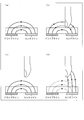
- FIG. 18 is a schematic diagram for explaining a change in capacitance between the drive line and the sense line due to touch input.
- 18A shows a case where there is no touch input
- FIG. 18B shows a case where there is a touch input by a detection target (for example, a finger or a pen tip of a touch pen) on the surface of the touch panel.
- FIG. 18C and FIG. 18D show a case where a detection target object related to touch input exists at a position away from the surface of the touch panel.
- the capacitance between the sense line and the drive line becomes small, and it becomes difficult to detect touch input.
- the electric force lines between the sense line and the drive line are terminated by the detection target. Changes.
- the detection object moves away from the surface of the touch panel as shown in FIG. 18 (c)
- the change in the capacitance becomes small because the electric force line between the sense line and the drive line is hardly changed.
- FIG. 18D there is a change in capacitance between the detection target and the sense line even when the detection target is slightly separated.
- the present inventor realizes detection of a touch input (detection object) existing at a position slightly away from the surface of the touch panel by utilizing the change in capacitance between the detection object and the sense line. I thought it was possible.
- Each of the embodiments embodying the present invention described below is devised based on the above-described new ideas that have not existed before.
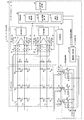
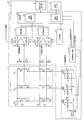
- FIG. 1 is a circuit diagram showing the configuration of the touch panel device 1a. As shown in the figure, the touch panel device 1a includes a touch panel 2 and a touch panel controller 3a.
- the touch panel 2 has M (M is an integer of 2 or more) drive lines DL 1 to DL M and N (N is an integer of 2 or more) sense lines SL 1 to SL N. Drive the line DL 1 ⁇ DL M and the sense lines SL 1 ⁇ SL N and cross position, the capacitance value C 1, 1 ⁇ C M each of the capacitance, the capacitance C 1, 1 ⁇ a N Each of CM and N is arranged in a matrix.
- Capacitances C Y, 1 to C Y, N correspond to capacitances (capacitance arrays) arranged in Y rows of a plurality of capacitances arranged in a matrix. It shall be.
- the output signal of the differential amplifier 6 is converted into a digital signal by the AD conversion unit 7, and then subjected to inner product calculation processing in the TP control unit 9a, and M electrostatic capacitances C 1, arranged in the row X of the sense line SLx . Capacitance values of X 1 to C M and X are estimated.
- the S1 control unit 8 displays “S1” and “ ⁇ S1” in the vicinity of each of the control signal S1 and the control signal ⁇ S1 (hereinafter, these control signals are collectively referred to as the S1 control signal SS). Controls the opening and closing of each switch. In the following, when the switch described as “S1” is open in the vicinity thereof, the switch described as “ ⁇ S1” is closed in the vicinity thereof, and conversely as “S1”. When the described switch is closed, the switch described as “ ⁇ S1” is open. That is, the control signal S1 and the control signal -S1 are in an inverted relationship with each other.
- the TP control unit 9a of the present embodiment includes an inner product calculation unit 91, a detection signal analysis unit (distance determination unit) 92, and a drive control unit (correlation control unit) 93.
- the inner product calculation unit 91 is based on (derived from) a linear sum that is output from at least one sense line SL X in the touch panel 2 and accumulated in each of a plurality of capacitances arranged in the corresponding row X. Capacitance values of a plurality of capacitances arranged in the corresponding row X of the sense line SL X are estimated by an inner product operation of the signal and a code sequence described later.
- the detection signal analysis unit 92 uses a capacitance value of each of the plurality of capacitances estimated by the inner product calculation unit 91, and a detection distance that is a distance between the surface of the touch panel 2 and the detection target is predetermined. It is determined whether or not it is larger than the threshold value.
- the “predetermined threshold value” includes “when the touch input is in contact with the touch panel surface, or when the touch input is not touched but the distance is sufficiently small” and “when the touch input is away from the touch panel surface”. This is a threshold value set for discrimination.
- the drive control unit 93 determines whether the correlation of the code sequences output from the drive signal generation units 4a to 4d is high or low depending on the determination result of whether or not the detection distance determined by the detection signal analysis unit 92 is larger than the threshold value. Control to switch between. More specifically, when the detection distance is equal to or smaller than the threshold, the drive control unit 93 causes the drive signal generation units 4a to 4d to output low correlation code sequences having low correlation as the code sequences. On the other hand, when the detection distance is larger than the threshold, the drive signal generation units 4a to 4d are made to output a high correlation code sequence having a high correlation with the low correlation code sequence as the code sequence.
- the drive signal generators 4a to 4d respectively send a plurality of drive signals for driving the M drive lines DL 1 to DL M in parallel to the capacitive drive unit 5 using a code sequence (or the same signal) described later. Output.
- the capacitance driving unit 5 converts the charges accumulated in each of the M electrostatic capacitances C 1, X 1 to C M, X arranged in the corresponding row X from at least one sense line SL X in the touch panel 2.
- the linear sum signal is output by driving the M drive lines DL 1 to DL M in parallel.
- Vd + Vcm and ⁇ Vd + Vcm are applied to the terminal TM + and the terminal TM ⁇ of the capacitance driving unit 5, respectively. Further, when the switch SW + of the capacity driving unit 5 is closed and the switch SW ⁇ is opened, Vd + Vcm is applied to each of the drive lines DL 1 to DL M. On the other hand, when the switch SW + of the capacity driving unit 5 is opened and the switch SW ⁇ is closed, ⁇ Vd + Vcm is applied to each of the drive lines DL 1 to DL M.
- one of the plurality of capacitances C M and N is driven by the capacitance driving unit 5 connected to the drive lines DL 1 to DL M.
- the capacity driver 5 is provided with code sequences D 1 to D M from the drive signal generators 4a to 4d.
- the capacity driving unit 5 applies the voltage Vd + Vcm to the corresponding drive line when the code of the code sequence is “1”, and applies the voltage ⁇ Vd + Vcm to the corresponding drive line when the code is “ ⁇ 1”.
- Vcm is a voltage serving as a reference for the drive voltage.
- each of the drive signal generators 4a to 4d When detecting the touch state when the detection target object is in contact with the surface of the touch panel 2 or not touching but the distance is sufficiently small (when the detection distance is equal to or less than the threshold value), Different code sequences are given. As this code sequence, it is desirable to use a code sequence having a low correlation with each other such as an M sequence, Hadamard sequence, or Walsh sequence (hereinafter, referred to as “low correlation code sequence” as appropriate).
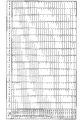
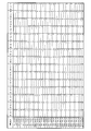
- FIGS. 14 and 15 show examples of Walsh sequences (Walsh codes). In these figures, for the sake of convenience, the first half and the second half of an example of the Walsh sequence are separated into two drawings of FIGS. That is, FIG.
- FIG. 14 shows code sequences from drive lines DL 1 to DL 16
- FIG. 15 shows code sequences from drive lines DL 17 to DL 32
- FIG. 16 shows an example of a Hadamard sequence (Hadamard code).
- FIG. 17 shows an example of a ternary M series.
- the code sequence applicable to the present invention is not limited to a binary code sequence. That is, it is also possible to use a multi-level code sequence of three or more values.
- the drive control unit 93 of the TP control unit 9a generates a low correlation code sequence as a drive signal generation unit when the distance (detection distance) between the surface of the touch panel 2 and the detection target is equal to or less than a predetermined threshold. Control to output to 4a to 4d is performed.
- the code sequence given to the capacity driving unit 5 is a code sequence having a high correlation with each other as compared with the low correlation code sequence. (Hereinafter referred to as “high correlation code sequence” as appropriate).
- the drive control unit 93 of the TP control unit 9a performs control to output the high correlation code sequence to the drive signal generation units 4a to 4d when the detection distance is larger than the threshold value.
- a highly correlated code sequence for example, by giving the same code sequence (or the same signal) to all the drive lines DL 1 to DL M , a highly correlated code sequence can be given. it can.
- an M-sequence using a linear feedback shift register is used as a code sequence (hereinafter referred to as an M-sequence code)
- the mode for embodying the present invention is not limited to such a mode.
- another code sequence orthogonal to each other may be used as the code sequence.
- the drive signal generators 4a to 4d include at least a linear feedback shift register (41) that outputs an M-sequence code and a plurality of shift registers 42 (corresponding to each of the plurality of drive lines DL 1 to DL M ). 1 to M).
- the drive signal generators 4a to 4d bit-shift the M sequence code output from the linear feedback shift register 41 by each of the plurality of shift registers 42 (1 to M), thereby generating M types of low correlation code signals. Output.
- the drive signal generators 4a to 4d provide the same signals as the plurality of drive signals to the drive lines DL 1 to DL M , respectively, thereby increasing the correlation of the code sequences and increasing the correlation. Outputs a code sequence. Thereby, the level of the correlation of a code sequence can be switched with a simple configuration.
- the drive signal generator 4a includes a first switch group 43 that operates according to the touch state control signal TS.
- the first switch group 43 outputs the outputs of the shift registers 42 (1 to M) according to the state control signal TS. Switching between the case where each signal is output and the state where all the output signals become the output signals of the shift register 1 are switched.
- an example in which the code sequence output from the shift register 1 is commonly given to all the drive lines DL 1 to DL M is shown as an example of the highly correlated code sequence.
- a code sequence output from any one shift register selected from the shift registers 42 (1 to M) may be given in common to all the drive lines DL1 to DLM. That is, in the drive signal generation unit 4a, when the detection distance is equal to or smaller than a predetermined threshold (when the touch input is in contact with the surface of the touch panel or not in contact but the distance is sufficiently small), the first switch group 43 is The output signals of the shift registers 42 (1 to M) are output according to the control signals. On the other hand, when the detection distance is larger than the threshold value (when the touch input is away from the touch panel surface), all output signals are the same as the output signals of the shift register 1.
- the drive signal generation unit 4a includes a second switch group 44 controlled by the same signal as the S1 control signal SS installed in the differential amplifier 6 shown in FIG.
- the switch SW + controlled by the control signal S1 is turned on (switch SW ⁇ is turned off)
- the second switch group 44 gives the output of the first switch group 43 to the drive lines DL 1 to DL M as they are.
- the switch SW + controlled by the control signal S1 is turned off (switch SW ⁇ is turned on)
- a signal obtained by inverting the output signal of the first switch group 43 is given to the drive lines DL 1 to DL M.
- a fixed signal (the same signal) and You may control so that it may become.
- GND ground potential
- the signal input to the shift register 1 may be controlled to be a fixed signal.
- FIG. 4 shows an example in which GND is used as the fixed signal. More specifically, when the detection distance is equal to or smaller than the threshold value, the switch SW1 is closed and the switch SW2 is opened. As a result, the M-sequence code from the linear feedback shift register 41 is supplied to each shift register 42 (1 to M), and the low correlation code sequence is applied to each drive line DL 1 to DL M. On the other hand, when the detection distance is larger than the threshold value, the switch SW1 is opened and the switch SW2 is closed. As a result, the signal input to the shift register 1 becomes a fixed signal (GND). As a result, the same fixed signal is supplied to each shift register 42 (1 to M), and a high correlation code sequence is applied to each drive line DL 1 to DL M.
- the linear feedback shift register is used as the code generation unit that outputs the sequence code.
- the code sequence may be generated by other methods.
- the drive signal generation unit may control the code generation unit that generates the code sequence by the touch state control signal TS. For example, when the touch input is away from the surface of the touch panel, all “1” or “ ⁇ A code sequence (or signal) such as “1” may be output.
- a fully differential amplifier is used as the differential amplifier 6, and adjacent sense lines are connected to the input / output side of the differential amplifier 6.
- the differential amplifier 6 does not have to be a fully differential amplifier, and adjacent sense lines do not necessarily have to be connected via the differential amplifier 6.
- Code sequence storage unit M 2 to 5 described above, as means for generating a code sequence, a linear feedback shift register 41 and a shift register 42 (corresponding to each of the plurality of drive lines DL 1 to DL M ) are provided. 1 to M) are shown, but the mode for embodying the present invention is not limited to this.
- data related to the code sequence is stored in advance in the code sequence storage unit M, and the drive control unit 93 of the TP control unit 9a sequentially reads out the code sequence recorded in the code sequence storage unit M, so that the drive signal You may supply to the capacity
- the code sequence storage unit M is not particularly required to be provided. That is, since the code sequence storage unit M is not provided, the memory capacity can be saved and the circuit configuration can be simplified.
- each voltage of the sense line is Vcm.
- Vd + Vcm is given to the drive lines DL 1 to DL M when the code sequence given thereto is “1”
- ⁇ Vd + Vcm is given when the code sequence is “ ⁇ 1”. Therefore, the charges Q1a and Q2a stored in the capacitors connected to the upper and lower two sense lines are Given in.
- C p1 and C p2 are capacitances between the sense lines and GND (ground potential).
- the estimated capacitance value is added to each of the M drive lines DL 1 to DL M. It becomes.
- each of a plurality of drive signals given to each of the drive lines DL 1 to DL M is correlated with each other. Switch to a higher signal. Briefly, the same signal is applied to all of the drive lines DL 1 to DL M.
- the output signal of the differential amplifier 6 is Given in.
- the estimated value in this case is It becomes.
- the influence of noise is about 1 / ⁇ M compared to the result of the above equation (2), which is more accurate.
- the capacity value can be estimated.
- the touch panel device 1a it is possible to more accurately detect the touch input by the detection object located slightly away from the surface of the touch panel 2.
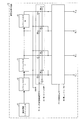
- FIG. 6 is a circuit diagram showing a configuration of a touch panel device (integrated circuit) 1b according to the second embodiment.
- the touch panel device 1a shown in the first embodiment when the sense line direction is the X axis and the drive line direction is the Y axis, the coordinate in the Y axis direction can be detected, but the coordinate in the X axis direction cannot be detected. There is a problem.
- FIG. 7 is a diagram for explaining a touch input coordinate detection function by the touch panel device according to the first embodiment and the second embodiment.
- FIG. 7 shows the state of the touch panel device 1a when the detection object related to the touch input (touch operation) is in contact with the surface of the touch panel 2 or is not in contact but the distance is sufficiently small. Yes.
- the sense lines SL 1 to SL N are physically separated, it is possible to separate the coordinates in the Y direction.
- each of the plurality of drive signals applied to each of the drive lines DL 1 to DL M is input to the same sense line through a plurality of capacitances, but there is a correlation between the plurality of drive signals (code sequences). Since it is low, the coordinates in the X direction can be separated.
- (b) of FIG. 7 shows the state of the touch panel device when the detection object related to the touch input exists at a position away from the surface of the touch panel.
- the sense lines SL 1 to SL N are physically separated, the coordinates in the Y direction can be separated as in the case of FIG. 7A.
- the same signal is given to each of the drive lines DL 1 to DL M , there arises a secondary problem that the coordinates in the Y direction cannot be separated.
- the present inventor combines the aspect of FIG. 7 (b) and the aspect of (c) of FIG. 7 when the detection target related to touch input exists at a position away from the surface of the touch panel. I thought that the above-mentioned secondary problems could be solved.
- the touch panel device 1b of the present embodiment includes switches that are controlled by an S1 control signal SS included in the switch group SB and the switch group SA (a switch controlled by the control signal S1 and a switch controlled by the control signal -S1). By switching between opening and closing, the function of the drive lines DL 1 to DL M and the function of the sense lines SL 1 to SL N can be switched.
- the S1 controller 8 controls the opening and closing of each switch included in the switch group SA to the switch group SC.
- the capacitance driving unit 5 is based on the electric charges accumulated in each of the plurality of capacitances C Y, 1 to C Y, N arranged in the corresponding column Y from at least one drive line DL Y in the touch panel 2.
- a (derived) linear sum signal (another linear sum signal) is output by driving a plurality of drive lines DL 1 to DL M in parallel.
- the touch panel device 1b it is possible to detect coordinates related to a two-dimensional touch input with reference to two directions of the sense line direction and the drive line direction (X direction and Y direction).
- the present inventor further supplies each voltage of the sense lines SL 1 to SL N when the switch controlled by the control signal S1 connected in parallel between the input terminal and the output terminal of the differential amplifier 6 is turned on to the drive line. It has been newly found that the influence of noise may be further reduced by changing according to a plurality of drive signals (code sequences) applied to DL 1 to DL M.
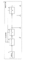
- the touch panel device 1c shown in FIG. 8 shows an example of a form using the above points.
- the S1 control unit (switching control unit) 8 enables the above switching by controlling the opening and closing of each switch included in the switch group SA to SC (switching means).
- the switch controlled by the control signal S1 included in the switch group SA is ON, the switch controlled by the control signal -S1 included in the switch group SB is OFF, and the switch group SC
- the switch controlled by the control signal S1 included in the switch group SA is OFF, the switch controlled by the control signal -S1 included in the switch group SB is ON, and controlled by the control signal S1 included in the switch group SC.
- the switch is turned off, the charge is distributed to the capacitance C int of the differential amplifier 6, the plurality of capacitances C 1, X to C M, X (capacitance array) arranged in the row X, and the ground capacitances Cp1, Cp2. Is done.
- the output (Vout t described later) of the differential amplifier 6 becomes a signal sent to the next stage.
- a switch that disconnects each of the sense lines SL 1 to SL N and the differential amplifier 6 when a switch controlled by the control signal S1 included in the switch group SA is turned ON is provided.
- a voltage that changes in accordance with the code sequence D1 applied to the drive lines DL 1 to DL M is applied to the line SL X.
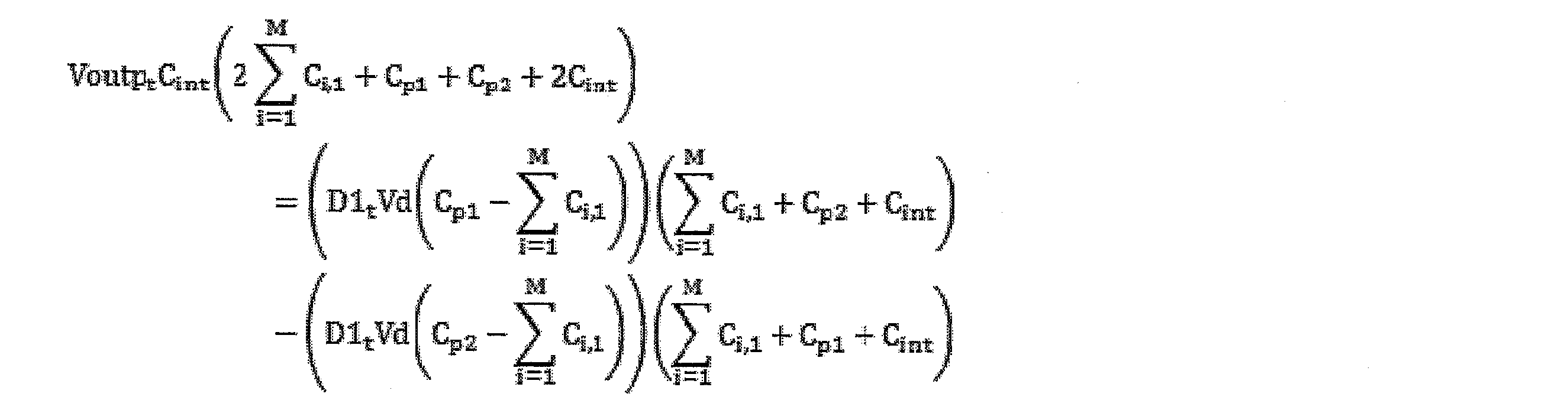
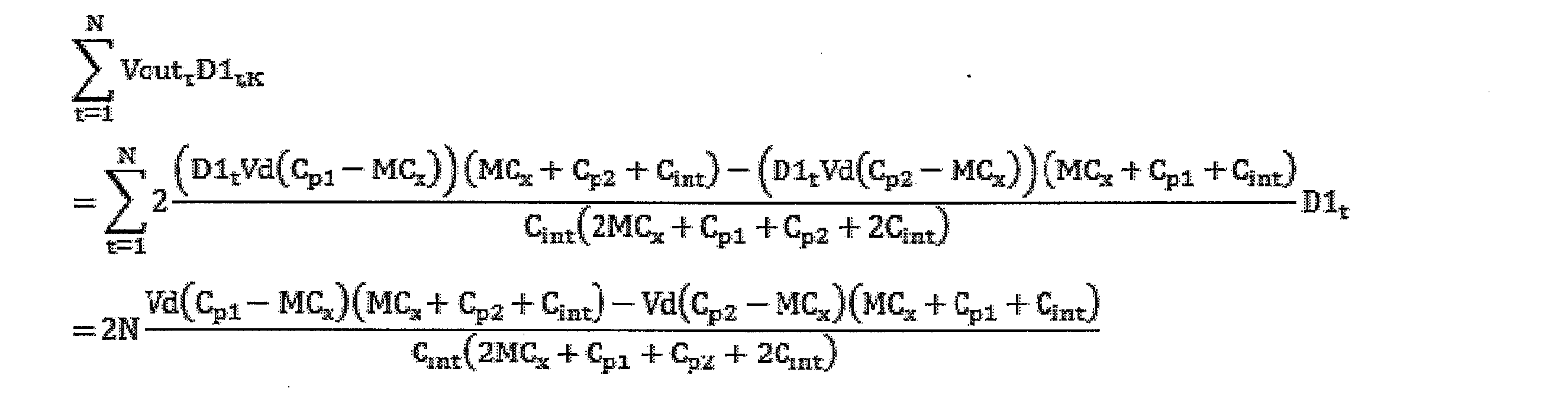
- the above-mentioned Q1a t, Q2a t is, It becomes.
- the estimated capacity value is It becomes.
- the configuration of the present embodiment can increase the coefficient for the estimated value of the capacitance value. The influence of noise can be further reduced.
- FIG. 9 is a block diagram showing a main configuration of the mobile phone 10 according to the present embodiment.
- the mobile phone 10 includes touch panel devices 1a to 1d, a display panel 11, a display control circuit 12, a CPU 13, a ROM 14, a RAM 15, a camera 16, a microphone 17, a speaker 18, and an operation.
- a key 19 is provided.
- the components of the mobile phone 10 are connected to each other by a data bus.
- the touch panel device 1 includes a touch panel 2 and touch panel controllers 3a to 3c.
- the touch panel devices 1a to 1d touch panel 2 and touch panel controllers 3a to 3c included in the mobile phone 10 according to the present embodiment are the same as any of the touch panel devices 1a to 1d according to the first to third embodiments and the fifth embodiment described later. Since it is the same, description is abbreviate
- the CPU 13 comprehensively controls the operation of the mobile phone 10.
- the CPU 13 controls the operation of the mobile phone 10 by executing a program stored in the ROM 14.
- a form in which the above-described TP control unit 9a and a TP control unit 9b to be described later are provided independently of the CPU 13 is described.
- the form for embodying the present invention is not limited thereto.
- the CPU 13 may have the functions of the TP control units 9a and 9b.
- the configuration of the touch panel controllers 3a to 3c can be simplified (refer to the form of FIG. 12 described later).
- the ROM (Read Only Memory) 14 is a readable and non-writable memory that stores fixed data such as a program executed by the CPU 13 such as an EPROM (Erasable Programmable Read-Only Memory).
- a RAM (Random Access Memory) 15 is a readable and writable memory, such as a flash memory, in which variable data such as data referred to by the CPU 13 for calculation and data generated by the CPU 13 is stored. .
- the operation key 19 receives an instruction input from the user to the mobile phone 10. Data input via the operation key 19 is stored in the RAM 15 in a volatile manner.
- the camera 16 shoots a subject based on a shooting instruction input by the user via the operation key 19.
- Image data of a subject photographed by the camera 16 is stored in the RAM 15 or an external memory (for example, a memory card).
- the microphone 17 receives the user's voice input.
- the input voice data (analog data) indicating the user's voice is converted into digital data by the mobile phone 10 and sent to another mobile phone (communication partner).
- the speaker 18 outputs sound represented by music data stored in the RAM 15 or the like, for example.
- the display control circuit 12 drives the display panel 11 to display an image represented by the image data stored in the ROM 14 or the RAM 15 based on a user instruction input via the operation key 19.
- the display panel 11 may be provided so as to overlap the touch panel 2, or may include the touch panel 2, and the configuration thereof is not particularly limited.
- the mobile phone 10 may further include an interface (IF) (not shown) for wired connection with other electronic devices.
- IF interface
- the mobile phone 10 since the mobile phone 10 according to the present embodiment includes any one of the touch panel devices 1a to 1d, the capacitance can be estimated more accurately, and thus the touch panel controllers 3a to 3c can be operated satisfactorily. It becomes possible. Therefore, since the mobile phone 10 can recognize the touch operation by the user more accurately, the mobile phone 10 can more accurately execute the process desired by the user.
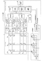
- the touch panel device 1d according to the present embodiment is provided with a distance sensor 20 (or a distance measuring sensor) instead of the detection signal analysis unit 92 according to the first embodiment.
- the TP control unit 9b of the touch panel device 1d includes only an inner product calculation unit 91 and a drive control unit (correlation control unit, distance determination unit) 93.
- the drive control unit 93 of the present embodiment determines whether or not the detection distance detected by the distance sensor 20 is greater than the predetermined threshold. Further, the drive control unit 93 performs control to switch the correlation of the code sequences output from the drive signal generation units 4a to 4d according to the determination result of whether or not the detection distance is larger than the threshold value. Therefore, if the correspondence relationship between the detection signal of the distance sensor 20 and the detection distance is examined in advance, it can be determined whether or not the detection distance is greater than the threshold value.
- an image sensor (an example of a distance measuring sensor) is provided in the vicinity of the display panel, and a touch state in the vicinity of the display panel is recognized by image analysis of an image captured by the image sensor.
- the embodiment embodying the present invention is not limited to this.
- the touch panel device incorporates a plurality of image sensors arranged in a plurality of matrices
- the image sensor is an example of a distance measuring sensor.
- the touch panel device 1e of the present embodiment excludes the TP control unit 9a and the code sequence storage unit M from the internal configuration of the touch panel controller 3a of the first embodiment, and instead, the role of the TP control unit 9a is changed to that of the touch panel device 1e.
- a form is shown in which the external CPU 13 is in charge and the role of the code sequence storage unit M is in the external ROM 14.
- the output data from the AD conversion unit 7 is directly input to the CPU 13, and the CPU 13 performs various information processing (similar to the processes of the inner product calculation unit 91, the detection signal analysis unit 92, and the drive control unit 93 described above). Process) to control the S1 control unit 8 and the drive signal generation units 4a to 4d in the touch panel controller 3e.
- the configuration of the touch panel controller itself can be extremely simplified because it is not necessary to provide the TP control unit and the code sequence storage unit inside the touch panel controller.
- the form in which the TP control unit 9a and the code sequence storage unit M are excluded from the internal configuration of the touch panel controller 3a in the first embodiment is shown, but the form in which the present invention is embodied is limited to this.
- the TP control unit 9a and the code sequence storage unit M are excluded from the touch panel controllers 3b to 3d of Embodiments 2 to 3 and 5, and the role of the TP control unit 9a is assigned to the external CPU 13 so that the code sequence storage unit M
- the form in which the role is assigned to the external ROM 14 is also included in the scope of the present invention.
- the touch panel controllers (3a to 3c) have a plurality of drive lines (DL 1 to DL) in which columns of a plurality of capacitances (C 11 to C MN ) arranged in a matrix are arranged. M ), and at least one sense line of the touch panel having a plurality of sense lines (SL 1 to SL N ) in which the plurality of rows of the plurality of capacitances are arranged, a plurality of static lines arranged in the corresponding row.
- the drive signal generation unit that outputs each of the drive signals to the capacitive drive unit, and a detection distance that is a distance between the surface of the touch panel and its detection target. Te, comprising correlation control unit that performs control to switch the high and low correlation of the code sequence (drive controller 93), the.
- the correlation control unit switches the level of the correlation of the code sequence according to the detection distance.
- the detection distance is a distance between the surface of the touch panel and its detection target.
- the present inventor detects a touch input by a detection object located at a position (slightly) away from the surface of the touch panel, if the correlation of the code sequence is increased, the correlation of the code sequence is not changed.
- the inventors have newly found that the influence of noise on a touch input detection signal (hereinafter referred to as a touch signal) can be reduced. Therefore, according to the said structure, the detection of the touch input by the detection target object in the position slightly away from the surface of the touch panel can be performed more correctly.
- the touch panel controller according to Aspect 2 of the present invention is the touch panel controller according to Aspect 1, wherein, when the detection distance is equal to or smaller than a predetermined threshold, the correlation control unit uses a low correlation code sequence having a low correlation as the code sequence as the drive signal. Control that causes the generation unit to output a high-correlation code sequence having a high correlation with the low-correlation code sequence as the code sequence when the detection distance is greater than the threshold value. May be performed.
- the correlation control unit when the detection distance is greater than the predetermined threshold, the correlation control unit outputs, as a code sequence, a high correlation code sequence having a high correlation with the low correlation code sequence to the drive signal generation unit.
- the “predetermined threshold value” includes “when the touch input is in contact with the touch panel surface, or when the touch input is not touched but the distance is sufficiently small” and “when the touch input is away from the touch panel surface”. This is a threshold value set for discrimination. Therefore, compared with the case where the correlation of the code sequence is not changed, it is possible to reduce the influence of noise when detecting the touch input by the detection target located slightly away from the surface of the touch panel.
- the touch panel controller according to Aspect 3 of the present invention is the touch panel controller according to Aspect 1 or 2, wherein the capacitance driving unit drives the plurality of sense lines in parallel, so that a column corresponding to at least one drive line in the touch panel is provided. Output another linear sum signal based on the charges accumulated in the plurality of capacitances arranged in the capacitor, and the drive signal generation unit causes the capacitance drive unit to drive the plurality of sense lines in parallel. Another linear sum signal may be output.
- the touch panel controller according to aspect 4 of the present invention is the touch panel controller according to aspects 1 to 3, in which the linear sum signal is output from the one sense line and the linear sum signal is not output from the one sense line.
- the voltage corresponding to a plurality of drive signals for driving the plurality of drive lines in parallel is applied to the output side of the one sense line, and the output A switching control unit (S1 control unit 8) that controls not to apply a voltage corresponding to the plurality of driving signals to the output side of the one sense line when switching to the mode may be provided.
- the influence of noise when detecting a touch input by a detection target located slightly away from the surface of the touch panel is further reduced as compared with the case where the above modes are not switched. be able to.
- the touch panel controller according to aspect 5 of the present invention is the touch panel controller according to aspect 2, in which the drive signal generation unit is provided corresponding to each of the linear feedback shift register (41) that outputs an M-sequence code and the plurality of drive lines.
- the correlation of the code sequences may be increased by generating the low correlation code sequence and applying the same signals as the plurality of drive signals to each of the plurality of drive lines.
- the correlation between code sequences can be switched with a simple configuration.
- the touch panel controller according to Aspect 6 of the present invention is the touch panel controller according to Aspects 1 to 5, in which a plurality of electrostatic capacitances arranged in a corresponding row of the one sense line are obtained by inner product calculation of the linear sum signal and the code sequence. You may provide the inner product calculating part (91) which estimates each capacitance value of a capacity
- the influence of noise when detecting a touch input by a detection target located slightly away from the surface of the touch panel is reduced, and arranged in a corresponding row of the one sense line. Capacitance values of a plurality of capacitances can be estimated.
- a touch panel controller includes a distance determination unit (detection signal analysis unit 93, drive control unit 93) that determines whether or not the detection distance is larger than the threshold value in aspect 6 above. Control for switching the correlation level of the code sequence output from the drive signal generation unit may be performed based on the determination result of the correlation control unit.
- the touch signal detected by the touch panel has a small signal range and a high signal level when the detection distance is small (when the distance between the surface of the touch panel and the detection target is short).
- the signal range tends to be large and the signal level tends to be small. Therefore, for example, if the correspondence between the detection distance and the touch signal is examined in advance using the above tendency, it is possible to determine whether or not the detection distance is larger than the threshold value.
- An integrated circuit, a touch panel device, and an electronic device including any one of the touch panel controllers according to the first to seventh aspects are also included in the scope of the present invention.
- the touch panel controller uses M code lines respectively formed between M drive lines (M is an integer of 2 or more) and one sense line as a code sequence.
- a touch panel controller including a drive unit (capacitance drive unit) that is driven in parallel with a signal based on the signal and outputs a linear sum signal based on the charges accumulated in the M capacitances from the sense line, A case where an inner product operation unit for estimating the M capacitance values is calculated by an inner product operation of one linear sum signal and the code sequence, and a first code sequence having a low correlation is used as the code sequence; You may switch the case where another code sequence with a mutual correlation high compared with a 1st code sequence is used.
- touch panel controller may be configured such that the sense line and the drive line can be interchanged with the touch panel controller described above.
- the touch panel controller may be any of the touch panel controllers described above, and may control a voltage of a terminal where the capacitance is not driven in accordance with a signal for driving the capacitance. .
- the integrated circuit according to one embodiment of the present invention may integrate any of the touch panel controllers described above.
- the touch panel device may include any one of the touch panel controllers described above and a touch panel controlled by the touch panel controller.
- an electronic device may include any one of the touch panel controllers described above and a touch panel controlled by the touch panel controller.
- the present invention can be used for a touch panel controller that estimates or detects a capacitance configured in a matrix by driving a plurality of drive lines in parallel, and an electronic device using the touch panel controller.
- the present invention can also be applied to a fingerprint detection system.
Landscapes
- Engineering & Computer Science (AREA)
- General Engineering & Computer Science (AREA)
- Theoretical Computer Science (AREA)
- Human Computer Interaction (AREA)
- Physics & Mathematics (AREA)
- General Physics & Mathematics (AREA)
- Computer Networks & Wireless Communication (AREA)
- Position Input By Displaying (AREA)
- Switches That Are Operated By Magnetic Or Electric Fields (AREA)
Abstract
Description





まず、図18に基づき、タッチ入力によるドライブラインおよびセンスライン間の静電容量の変化について説明する。図18は、タッチ入力によるドライブラインおよびセンスライン間の静電容量の変化を説明するための模式図である。図18の(a)は、タッチ入力が存在しない場合を示し、図18の(b)は、タッチパネルの表面に検出対象物(例えば、指やタッチペンのペン先など)によるタッチ入力がある場合を示し、図18の(c)および図18の(d)は、タッチパネルの表面から離れた位置にタッチ入力に係る検出対象物が存在している場合を示す。
以下、図1~図5を参照して、本発明の実施形態1に係るタッチパネル装置(集積回路)1aについて説明する。
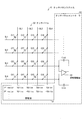
図1にタッチパネル装置1aの構成を示す回路図を示す。同図に示すように、タッチパネル装置1aは、タッチパネル2およびタッチパネルコントローラ3aを備えている。
タッチパネル2は、M本(Mは2以上の整数)のドライブラインDL1~DLMと、N本(Nは2以上の整数)のセンスラインSL1~SLNとを有している。ドライブラインDL1~DLMとセンスラインSL1~SLNとが交差する位置には、静電容量の容量値がそれぞれC1,1~CM,Nである静電容量C1,1~CM,Nのそれぞれがマトリクス状に配置されている。なお、以下では、静電容量C1,X~CM,X(x=1~N)は、マトリクス状に配置された複数の静電容量のX行に配置された静電容量(容量アレイ)に対応するものとする。また、静電容量CY,1~CY,N(Y=1~M)は、マトリクス状に配置された複数の静電容量のY列に配置された静電容量(容量アレイ)に対応するものとする。
図1に示すように、タッチパネルコントローラ3aは、駆動信号生成部4a~4d、容量駆動部5、差動増幅器6、AD変換部7、S1制御部8、およびTP(タッチパネル)制御部9aを備えている。なお、タッチパネルコントローラ3aは、図1に示す符号系列記憶部Mを必ずしも備えていなくても良いが、以下の説明にて登場するため、図1では説明の便宜上、タッチパネルコントローラ3aの構成に含めている。また、各センスラインSLx(X=1~N)の出力端子側には、そのラインに沿う方向(以下、「センスライン方向」という)の左側から右側に向けて、対地容量Cpx、差動増幅器6、およびAD変換器7がこの順で接続されている。また、各差動増幅器6の入力端子-出力端子間には、静電容量Cintおよび制御信号S1にて開閉を制御されるスイッチが並列接続されている。
差動増幅器6の出力信号はAD変換部7によってデジタル信号に変換された後にTP制御部9aにて内積演算処理を行いセンスラインSLxの行Xに配置されたM個の静電容量C1,X~CM,Xのそれぞれの容量値が推定される。
S1制御部8は、制御信号S1および制御信号-S1(以下、これらの制御信号を纏めてS1制御信号SSと称する)のそれぞれで、その近傍に「S1」および「-S1」と表示されている各スイッチの開閉を制御する。なお、以下、その近傍にて「S1」と記載されているスイッチが開いている場合、その近傍にて「-S1」と記載されているスイッチは閉じているものとし、逆に「S1」と記載されているスイッチが閉じている場合、「-S1」と記載されたスイッチは開いているものとする。すなわち、制御信号S1と、制御信号-S1とは、互いに反転の関係にある。
本実施形態のTP制御部9aは、内積演算部91、検出信号解析部(距離判定部)92、駆動制御部(相関制御部)93を備える。
検出信号解析部92は、内積演算部91によって推定された上記複数の静電容量のそれぞれの容量値を用いて、タッチパネル2の表面と検出対象物との間の距離である検出距離が所定の閾値よりも大きいか否かを判定する。ここで、「所定の閾値」は、「タッチ入力がタッチパネル表面に接触している、または接触していないが距離が十分小さい場合」と、「タッチ入力がタッチパネル表面から離れている場合」とを判別するために設定される閾値である。また、駆動制御部93は、検出信号解析部92によって判定される上記検出距離が上記閾値よりも大きいか否かの判定結果によって、駆動信号生成部4a~4dが出力する符号系列の相関の高低を切り替える制御を行う。より具体的には、駆動制御部93は、上記検出距離が上記閾値以下の場合に、上記符号系列として互いに相関の低い低相関符号系列を駆動信号生成部4a~4dに出力させる。一方、上記検出距離が上記閾値よりも大きい場合に、上記符号系列として上記低相関符号系列と比較して互いの相関が高い高相関符号系列を駆動信号生成部4a~4dに出力させる。
駆動信号生成部4a~4dは、後述する符号系列(または互いに同一の信号)を用いてM本のドライブラインDL1~DLMを並列駆動させる複数の駆動信号のそれぞれを容量駆動部5に対して出力する。容量駆動部5は、タッチパネル2における少なくとも一本のセンスラインSLXから、対応する行Xに配置されたM個の静電容量C1,X~CM,Xのそれぞれに蓄積された電荷に基づく線形和信号を、M本のドライブラインDL1~DLMを並列駆動させることで出力させる。容量駆動部5の端子TM+および端子TM-のそれぞれには、Vd+Vcmおよび-Vd+Vcmが印加されている。また、容量駆動部5のスイッチSW+が閉じ、スイッチSW-が開いている場合には、ドライブラインDL1~DLMのそれぞれには、Vd+Vcmが印加される。一方、容量駆動部5のスイッチSW+が開き、スイッチSW-が閉じている場合には、ドライブラインDL1~DLMのそれぞれには、-Vd+Vcmが印加される。
上述した図2~5に示した各形態では、符号系列を生成する手段として、線形帰還シフトレジスタ41と、複数のドライブラインDL1~DLMのそれぞれに対応して配置されるシフトレジスタ42(1~M)とを用いる例を示したが、本発明を具現化する形態は、これに限定されない。例えば、符号系列記憶部Mに、予め符号系列に関するデータを格納しておき、TP制御部9aの駆動制御部93が、符号系列記憶部Mに記録されている符号系列を順次読出して、駆動信号生成部を介して容量駆動部5に供給しても良い。なお、駆動信号生成部として、上記の駆動信号生成部4a~4dを用いる場合には、特に符号系列記憶部Mを設ける必要はない。すなわち、符号系列記憶部Mを設けない分、メモリ容量の節約ができ、かつ回路構成を簡単にできる。
次に、図10を用いて、タッチパネル装置1aの作用効果について詳細に説明する。

















図6は、実施形態2に係るタッチパネル装置(集積回路)1bの構成を示す回路図である。上記の実施形態1に示したタッチパネル装置1aでは、センスライン方向をX軸、ドライブライン方向をY軸とした場合、Y軸方向の座標の検出はできるがX軸方向の座標の検出ができないという問題点がある。そこで、まず、図7に基づき、上記の問題点について詳細に説明する。図7は、上記実施形態1および上記実施形態2に係るタッチパネル装置によるタッチ入力の座標の検出機能を説明するための図である。
本発明者は、さらに、差動増幅器6の入力端子-出力端子間に並列接続された制御信号S1で制御されるスイッチがONとなる場合のセンスラインSL1~SLNの各電圧をドライブラインDL1~DLMに与える複数の駆動信号(符号系列)に応じて変更することで、さらにノイズの影響を軽減できる場合がある点を新たに見出した。図8に示すタッチパネル装置1cは、以上の点を利用した形態の一例を示す。
(1)ある一本のセンスラインから線形和信号を出力しない場合に、複数のドライブラインDL1~DLMを並列駆動させる複数の駆動信号に応じた電圧を上記一本のセンスラインの出力側に印加するモード(非出力モード)と、
(2)上記一本のセンスラインから線形和信号を出力する場合に、上記複数の駆動信号に応じた電圧を上記一本のセンスラインの出力側に印加しないモード(出力モード)と、を切り替える。
次に、図10を用いて、タッチパネル装置1cの作用効果について詳細に説明する。








次に、実施形態1~3および後述する実施形態5に係るタッチパネル装置1a~1dのいずれかを備える電子機器の一例として、携帯電話機(電子機器)10について、図9を参照して説明する。図9は、本実施形態に係る携帯電話機10の要部構成を示すブロック図である。
本実施形態に係る携帯電話機10は、図9に示すように、タッチパネル装置1a~1d、表示パネル11、表示制御回路12、CPU13、ROM14、RAM15、カメラ16、マイクロフォン17、スピーカ18、および、操作キー19を備えている。また、携帯電話機10の各構成要素は、相互にデータバスによって接続されている。
次に、図11に基づき、本発明の実施形態5に係るタッチパネル装置(集積回路)1dの構成について説明する。
次に、図12に基づき、本発明の実施形態6に係るタッチパネル装置(集積回路)1eの構成について説明する。
本発明の態様1に係るタッチパネルコントローラ(3a~3c)は、マトリクス状に配置された複数の静電容量(C11~CMN)の各列が配置された複数のドライブライン(DL1~DLM)、および上記複数の静電容量の各行が配置された複数のセンスライン(SL1~SLN)を備えたタッチパネルの少なくとも一本のセンスラインから、対応する行に配置された複数の静電容量に蓄積される電荷に基づく線形和信号を、上記複数のドライブラインを並列駆動させることで出力させる容量駆動部(5)と、符号系列を用いて上記複数のドライブラインを並列駆動させる複数の駆動信号のそれぞれを上記容量駆動部に対して出力する駆動信号生成部と、上記タッチパネルの表面とその検出対象物との間の距離である検出距離に応じて、上記符号系列の相関の高低を切り替える制御を行う相関制御部(駆動制御部93)と、を備える。
本発明は以下のように表現することもできる。
本発明は上述した各実施形態に限定されるものではなく、請求項に示した範囲で種々の変更が可能であり、異なる実施形態にそれぞれ開示された技術的手段を適宜組み合わせて得られる実施形態についても本発明の技術的範囲に含まれる。さらに、各実施形態にそれぞれ開示された技術的手段を組み合わせることにより、新しい技術的特徴を形成することができる。
2 タッチパネル
3a~3e タッチパネルコントローラ
4a~4d 駆動信号生成部
5 容量駆動部
8 S1制御部(切替制御部)
10 携帯電話機(電子機器)
20 距離センサ
41 線形帰還シフトレジスタ
42 シフトレジスタ(1~M)
91 内積演算部
92 検出信号解析部(距離判定部)
93 駆動制御部(相関制御部,距離判定部)
Cint 静電容量
CM,N 静電容量
DLM ドライブライン
SLN センスライン
Claims (10)
- マトリクス状に配置された複数の静電容量の各列が配置された複数のドライブライン、および上記複数の静電容量の各行が配置された複数のセンスラインを備えたタッチパネルの少なくとも一本のセンスラインから、対応する行に配置された複数の静電容量に蓄積される電荷に基づく線形和信号を、上記複数のドライブラインを並列駆動させることで出力させる容量駆動部と、
符号系列を用いて上記複数のドライブラインを並列駆動させる複数の駆動信号のそれぞれを上記容量駆動部に対して出力する駆動信号生成部と、
上記タッチパネルの表面とその検出対象物との間の距離である検出距離に応じて、上記符号系列の相関の高低を切り替える制御を行う相関制御部と、を備えることを特徴とするタッチパネルコントローラ。 - 上記相関制御部は、
上記検出距離が所定の閾値よりも小さい場合に、上記符号系列として互いに相関の低い低相関符号系列を上記駆動信号生成部に出力させ、
上記検出距離が上記閾値以上の場合に、上記符号系列として上記低相関符号系列と比較して互いの相関が高い高相関符号系列を上記駆動信号生成部に出力させる制御を行うことを特徴とする請求項1に記載のタッチパネルコントローラ。 - 上記容量駆動部は、
上記複数のセンスラインを並列駆動させることで、上記タッチパネルにおける少なくとも一本のドライブラインから、対応する列に配置された複数の静電容量に蓄積される電荷に基づく別の線形和信号を出力し、
上記駆動信号生成部は、上記容量駆動部に、上記複数のセンスラインを並列駆動させることで上記別の線形和信号を出力させることを特徴とする請求項1または2に記載のタッチパネルコントローラ。 - 上記一本のセンスラインから上記線形和信号を出力する出力モードと、上記一本のセンスラインから上記線形和信号を出力しない非出力モードとを切り替え、
上記非出力モードに切り替えた場合に、上記複数のドライブラインを並列駆動させる複数の駆動信号に応じた電圧を上記一本のセンスラインの出力側に印加し、
上記出力モードに切り替えた場合に、上記複数の駆動信号に応じた電圧を上記一本のセンスラインの出力側に印加しないように制御する切替制御部を備えることを特徴とする請求項1から3までのいずれか1項に記載のタッチパネルコントローラ。 - 上記駆動信号生成部は、
M系列符号を出力する線形帰還シフトレジスタと、
上記複数のドライブラインのそれぞれに対応して設けられた複数のシフトレジスタと、を備え、
上記線形帰還シフトレジスタから出力される上記M系列符号を、上記複数のシフトレジスタのそれぞれでビットシフトさせることで、複数種類の上記低相関符号系列を生成し、
上記複数のドライブラインのそれぞれに、上記複数の駆動信号として、互いに同一の信号を与えることで、上記符号系列の相関を高くすることを特徴とする請求項2に記載のタッチパネルコントローラ。 - 上記線形和信号と上記符号系列との内積演算により、上記一本のセンスラインの対応する行に配置された複数の静電容量のそれぞれの容量値を推定する内積演算部を備えていることを特徴とする請求項1から5までのいずれか1項に記載のタッチパネルコントローラ。
- 上記検出距離が上記閾値よりも大きいか否かを判定する距離判定部を備え、上記相関制御部は、上記距離判定部の判定結果によって、上記駆動信号生成部が出力する上記符号系列の相関の高低を切り替える制御を行うことを特徴とする請求項2に記載のタッチパネルコントローラ。
- 請求項1から7までのいずれか1項に記載のタッチパネルコントローラを備えることを特徴とする集積回路。
- 請求項1から7までのいずれか1項に記載のタッチパネルコントローラを備えることを特徴とするタッチパネル装置。
- 請求項1から7までのいずれか1項に記載のタッチパネルコントローラを備えることを特徴とする電子機器。
Priority Applications (3)
| Application Number | Priority Date | Filing Date | Title |
|---|---|---|---|
| CN201480035013.0A CN105308547A (zh) | 2013-06-20 | 2014-04-09 | 触摸面板控制器、集成电路、触摸面板装置和电子设备 |
| US14/889,765 US9658728B2 (en) | 2013-06-20 | 2014-04-09 | Touch panel controller, integrated circuit, touch panel device, and electronic device |
| JP2015522614A JP5973072B2 (ja) | 2013-06-20 | 2014-04-09 | タッチパネルコントローラ、集積回路、タッチパネル装置、および電子機器 |
Applications Claiming Priority (2)
| Application Number | Priority Date | Filing Date | Title |
|---|---|---|---|
| JP2013129904 | 2013-06-20 | ||
| JP2013-129904 | 2013-06-20 |
Publications (1)
| Publication Number | Publication Date |
|---|---|
| WO2014203598A1 true WO2014203598A1 (ja) | 2014-12-24 |
Family
ID=52104342
Family Applications (1)
| Application Number | Title | Priority Date | Filing Date |
|---|---|---|---|
| PCT/JP2014/060304 Ceased WO2014203598A1 (ja) | 2013-06-20 | 2014-04-09 | タッチパネルコントローラ、集積回路、タッチパネル装置、および電子機器 |
Country Status (4)
| Country | Link |
|---|---|
| US (1) | US9658728B2 (ja) |
| JP (1) | JP5973072B2 (ja) |
| CN (1) | CN105308547A (ja) |
| WO (1) | WO2014203598A1 (ja) |
Families Citing this family (6)
| Publication number | Priority date | Publication date | Assignee | Title |
|---|---|---|---|---|
| JP5973072B2 (ja) * | 2013-06-20 | 2016-08-23 | シャープ株式会社 | タッチパネルコントローラ、集積回路、タッチパネル装置、および電子機器 |
| US10082916B2 (en) * | 2015-07-08 | 2018-09-25 | Samsung Electronics Co., Ltd. | Circuit for cancelling offset capacitance of capacitive touch screen panel and device including the same |
| KR102511952B1 (ko) * | 2016-01-18 | 2023-03-23 | 삼성디스플레이 주식회사 | 터치 스크린 패널 및 그의 구동 방법 |
| CN107526993A (zh) * | 2016-06-20 | 2017-12-29 | 康达生命科学有限公司 | 电容式指纹传感器 |
| TWI613636B (zh) * | 2016-12-28 | 2018-02-01 | 財團法人工業技術研究院 | 驅動裝置以及驅動方法 |
| TWI712020B (zh) * | 2019-10-04 | 2020-12-01 | 凌巨科技股份有限公司 | 顯示裝置 |
Citations (3)
| Publication number | Priority date | Publication date | Assignee | Title |
|---|---|---|---|---|
| JP2008117371A (ja) * | 2006-10-13 | 2008-05-22 | Sony Corp | 近接検知型情報表示装置およびこれを使用した情報表示方法 |
| JP2012247870A (ja) * | 2011-05-25 | 2012-12-13 | Sharp Corp | 静電容量推定方法、集積回路、及び電子機器 |
| JP2013092872A (ja) * | 2011-10-25 | 2013-05-16 | Sharp Corp | タッチパネルシステムおよび電子機器 |
Family Cites Families (39)
| Publication number | Priority date | Publication date | Assignee | Title |
|---|---|---|---|---|
| US7868874B2 (en) * | 2005-11-15 | 2011-01-11 | Synaptics Incorporated | Methods and systems for detecting a position-based attribute of an object using digital codes |
| US8605054B2 (en) * | 2010-09-02 | 2013-12-10 | Texas Instruments Incorporated | Touch-sensitive interface and method using orthogonal signaling |
| WO2012039837A1 (en) * | 2010-09-22 | 2012-03-29 | Cypress Semiconductor Corporation | Capacitive stylus for a touch screen |
| JP4927216B1 (ja) * | 2010-11-12 | 2012-05-09 | シャープ株式会社 | 線形素子列値推定方法、静電容量検出方法、集積回路、タッチセンサシステム、及び電子機器 |
| JP4955116B1 (ja) * | 2010-12-28 | 2012-06-20 | シャープ株式会社 | タッチパネルシステムおよび電子機器 |
| JP5231605B2 (ja) * | 2011-06-10 | 2013-07-10 | シャープ株式会社 | タッチパネルコントローラ、及びこれを用いた電子機器 |
| WO2012176857A1 (en) * | 2011-06-22 | 2012-12-27 | Sharp Kabushiki Kaisha | Touch panel system and electronic device |
| JP5539269B2 (ja) * | 2011-06-27 | 2014-07-02 | シャープ株式会社 | 静電容量値分布検出方法、静電容量値分布検出回路、タッチセンサシステム、及び情報入出力機器 |
| TWI518565B (zh) * | 2011-06-22 | 2016-01-21 | 夏普股份有限公司 | 觸控面板系統及電子機器 |
| JP5384598B2 (ja) * | 2011-09-09 | 2014-01-08 | シャープ株式会社 | 静電容量型タッチセンサパネル、及びこれを用いた静電容量型タッチセンサシステム、情報入出力装置 |
| JP5350437B2 (ja) * | 2011-06-27 | 2013-11-27 | シャープ株式会社 | タッチセンサシステム |
| TWI524224B (zh) * | 2011-06-22 | 2016-03-01 | 夏普股份有限公司 | 觸控面板系統及電子機器 |
| TWI502418B (zh) * | 2011-06-22 | 2015-10-01 | Sharp Kk | 觸摸面板系統及電子裝置 |
| WO2013001920A1 (en) * | 2011-06-29 | 2013-01-03 | Sharp Kabushiki Kaisha | Touch sensor system and electronic device |
| WO2013018625A1 (ja) * | 2011-07-29 | 2013-02-07 | シャープ株式会社 | 表示装置 |
| US9310911B2 (en) * | 2011-07-29 | 2016-04-12 | Sharp Kabushiki Kaisha | Display device |
| JP5296185B2 (ja) * | 2011-12-21 | 2013-09-25 | シャープ株式会社 | タッチセンサシステム |
| JP5490828B2 (ja) * | 2012-01-10 | 2014-05-14 | シャープ株式会社 | 線形系係数推定方法及びそれを用いた集積回路、タッチパネルシステム、及び電子機器 |
| WO2013129742A1 (en) * | 2012-02-29 | 2013-09-06 | Lg Innotek Co., Ltd. | Position sensing method of touch panel and integrated circuit |
| JP5341224B2 (ja) * | 2012-04-04 | 2013-11-13 | シャープ株式会社 | タッチパネルコントローラ、集積回路、タッチパネルシステム、及び電子機器 |
| JP5886139B2 (ja) * | 2012-05-30 | 2016-03-16 | シャープ株式会社 | タッチセンサシステム |
| JP5394540B2 (ja) * | 2012-06-25 | 2014-01-22 | シャープ株式会社 | タッチパネルコントローラ、集積回路、タッチパネル装置、及び電子機器。 |
| JP5740534B2 (ja) * | 2012-09-11 | 2015-06-24 | シャープ株式会社 | 信号処理システム、タッチパネルコントローラ、並びに、これを用いたタッチパネルシステム及び電子機器 |
| CN104813262B (zh) * | 2012-11-30 | 2016-05-18 | 夏普株式会社 | 触摸面板控制器和使用其的电子设备 |
| WO2014129375A1 (ja) * | 2013-02-25 | 2014-08-28 | シャープ株式会社 | 電子機器および情報処理システム |
| US9678613B2 (en) * | 2013-02-25 | 2017-06-13 | Sharp Kabushiki Kaisha | Input device and display |
| JP6105054B2 (ja) * | 2013-04-05 | 2017-03-29 | シャープ株式会社 | タッチパネル位置検出方法、タッチパネルコントローラ、タッチパネルシステム、及び電子機器 |
| US9001066B2 (en) * | 2013-05-06 | 2015-04-07 | Rajkumari Mohindra | PAPR optimized OFDM touch engine with tone spaced windowed demodulation |
| WO2014181680A1 (ja) * | 2013-05-10 | 2014-11-13 | シャープ株式会社 | タッチパネルシステム、スタイラスペン、及び電子機器 |
| US9501091B2 (en) * | 2013-05-17 | 2016-11-22 | Sharp Kabushiki Kaisha | Touch panel system and electronic device |
| US9495056B2 (en) * | 2013-05-21 | 2016-11-15 | Sharp Kabushiki Kaisha | Touch panel system and electronic device |
| WO2014196350A1 (ja) * | 2013-06-07 | 2014-12-11 | シャープ株式会社 | タッチパネルシステム及び電子機器 |
| JP5973072B2 (ja) * | 2013-06-20 | 2016-08-23 | シャープ株式会社 | タッチパネルコントローラ、集積回路、タッチパネル装置、および電子機器 |
| WO2014208189A1 (ja) * | 2013-06-24 | 2014-12-31 | シャープ株式会社 | タッチパネルコントローラ、集積回路、及び電子機器 |
| JP5969127B2 (ja) * | 2013-06-28 | 2016-08-17 | シャープ株式会社 | タッチパネルコントローラ及び電子機器 |
| WO2015002203A1 (ja) * | 2013-07-05 | 2015-01-08 | シャープ株式会社 | タッチパネルシステム |
| US10042483B2 (en) * | 2014-04-18 | 2018-08-07 | Atmel Corporation | Touch system with code hopping algorithms and code division multiplexing |
| KR20160018188A (ko) * | 2014-08-08 | 2016-02-17 | 삼성전기주식회사 | 터치스크린 장치, 터치 감지 방법 및 구동 신호 및 구동 행렬의 생성 방법 |
| KR102367957B1 (ko) * | 2014-12-29 | 2022-02-25 | 삼성디스플레이 주식회사 | 접촉 감지 장치 및 이의 구동방법 |
-
2014
- 2014-04-09 JP JP2015522614A patent/JP5973072B2/ja not_active Expired - Fee Related
- 2014-04-09 CN CN201480035013.0A patent/CN105308547A/zh active Pending
- 2014-04-09 WO PCT/JP2014/060304 patent/WO2014203598A1/ja not_active Ceased
- 2014-04-09 US US14/889,765 patent/US9658728B2/en active Active
Patent Citations (3)
| Publication number | Priority date | Publication date | Assignee | Title |
|---|---|---|---|---|
| JP2008117371A (ja) * | 2006-10-13 | 2008-05-22 | Sony Corp | 近接検知型情報表示装置およびこれを使用した情報表示方法 |
| JP2012247870A (ja) * | 2011-05-25 | 2012-12-13 | Sharp Corp | 静電容量推定方法、集積回路、及び電子機器 |
| JP2013092872A (ja) * | 2011-10-25 | 2013-05-16 | Sharp Corp | タッチパネルシステムおよび電子機器 |
Also Published As
| Publication number | Publication date |
|---|---|
| CN105308547A (zh) | 2016-02-03 |
| US20160132149A1 (en) | 2016-05-12 |
| JP5973072B2 (ja) | 2016-08-23 |
| JPWO2014203598A1 (ja) | 2017-02-23 |
| US9658728B2 (en) | 2017-05-23 |
Similar Documents
| Publication | Publication Date | Title |
|---|---|---|
| JP5973072B2 (ja) | タッチパネルコントローラ、集積回路、タッチパネル装置、および電子機器 | |
| CN103649888B (zh) | 线性器件值估计方法、电容检测方法、集成电路、触摸传感器系统以及电子设备 | |
| KR102267365B1 (ko) | 다단 증분 스위칭 체계 | |
| US8519975B2 (en) | Detector and detection method for a capacitive touchpad to identify a real touch point | |
| JPWO2014174960A1 (ja) | スタイラスペン、タッチパネルシステム、および電子機器 | |
| JP5490828B2 (ja) | 線形系係数推定方法及びそれを用いた集積回路、タッチパネルシステム、及び電子機器 | |
| JP6105054B2 (ja) | タッチパネル位置検出方法、タッチパネルコントローラ、タッチパネルシステム、及び電子機器 | |
| US20150253926A1 (en) | Semiconductor device and electronic apparatus | |
| WO2013151060A1 (ja) | タッチパネルコントローラ、集積回路、タッチパネルシステム、及び電子機器 | |
| JP5989906B2 (ja) | タッチパネルコントローラ、集積回路、及び電子機器 | |
| US20150338955A1 (en) | Touch panel controller and electronic device using same | |
| JP5394540B2 (ja) | タッチパネルコントローラ、集積回路、タッチパネル装置、及び電子機器。 | |
| JP5969127B2 (ja) | タッチパネルコントローラ及び電子機器 | |
| CN102193694A (zh) | 补偿电容偏差的电子装置 | |
| JP2013149223A (ja) | 線形系係数推定方法及びそれを用いた集積回路、タッチパネル装置、及び電子機器 | |
| JP2015118553A (ja) | タッチパネルコントローラ、タッチパネル装置、及び電子機器 | |
| US9874986B2 (en) | Compensation for variations in a capacitive sense matrix | |
| KR20180024701A (ko) | 터치 검출 방법 및 이를 이용하는 터치 검출 장치 | |
| JP2015007912A (ja) | タッチパネルコントローラ、及び電子機器 | |
| JP5449461B2 (ja) | タッチパネルコントローラ、及びこれを用いた集積回路、タッチパネル装置、電子機器 | |
| US9195355B2 (en) | Method for increasing accuracy of touch coordinate calculation in a capacitive multi-touch system | |
| US20130127746A1 (en) | Method for controlling touch panel | |
| JP2015153109A (ja) | タッチパネルコントローラ、タッチパネル装置、及び、電子機器 | |
| WO2014208174A1 (ja) | タッチパネルコントローラ、タッチパネルシステム、および電子機器 | |
| US10055045B2 (en) | Current feedback digital charge accumulator |
Legal Events
| Date | Code | Title | Description |
|---|---|---|---|
| WWE | Wipo information: entry into national phase |
Ref document number: 201480035013.0 Country of ref document: CN |
|
| 121 | Ep: the epo has been informed by wipo that ep was designated in this application |
Ref document number: 14813831 Country of ref document: EP Kind code of ref document: A1 |
|
| ENP | Entry into the national phase |
Ref document number: 2015522614 Country of ref document: JP Kind code of ref document: A |
|
| WWE | Wipo information: entry into national phase |
Ref document number: 14889765 Country of ref document: US |
|
| NENP | Non-entry into the national phase |
Ref country code: DE |
|
| 122 | Ep: pct application non-entry in european phase |
Ref document number: 14813831 Country of ref document: EP Kind code of ref document: A1 |