WO2014203447A1 - 積層インダクタ - Google Patents
積層インダクタ Download PDFInfo
- Publication number
- WO2014203447A1 WO2014203447A1 PCT/JP2014/002577 JP2014002577W WO2014203447A1 WO 2014203447 A1 WO2014203447 A1 WO 2014203447A1 JP 2014002577 W JP2014002577 W JP 2014002577W WO 2014203447 A1 WO2014203447 A1 WO 2014203447A1
- Authority
- WO
- WIPO (PCT)
- Prior art keywords
- coil
- permanent magnet
- multilayer inductor
- layer
- magnetic
- Prior art date
- Legal status (The legal status is an assumption and is not a legal conclusion. Google has not performed a legal analysis and makes no representation as to the accuracy of the status listed.)
- Ceased
Links
Images






Classifications
-
- H—ELECTRICITY
- H01—ELECTRIC ELEMENTS
- H01F—MAGNETS; INDUCTANCES; TRANSFORMERS; SELECTION OF MATERIALS FOR THEIR MAGNETIC PROPERTIES
- H01F27/00—Details of transformers or inductances, in general
- H01F27/24—Magnetic cores
- H01F27/255—Magnetic cores made from particles
-
- H—ELECTRICITY
- H01—ELECTRIC ELEMENTS
- H01F—MAGNETS; INDUCTANCES; TRANSFORMERS; SELECTION OF MATERIALS FOR THEIR MAGNETIC PROPERTIES
- H01F17/00—Fixed inductances of the signal type
- H01F17/0006—Printed inductances
- H01F17/0013—Printed inductances with stacked layers
-
- H—ELECTRICITY
- H01—ELECTRIC ELEMENTS
- H01F—MAGNETS; INDUCTANCES; TRANSFORMERS; SELECTION OF MATERIALS FOR THEIR MAGNETIC PROPERTIES
- H01F17/00—Fixed inductances of the signal type
- H01F17/0006—Printed inductances
- H01F17/0033—Printed inductances with the coil helically wound around a magnetic core
-
- H—ELECTRICITY
- H01—ELECTRIC ELEMENTS
- H01F—MAGNETS; INDUCTANCES; TRANSFORMERS; SELECTION OF MATERIALS FOR THEIR MAGNETIC PROPERTIES
- H01F21/00—Variable inductances or transformers of the signal type
-
- H—ELECTRICITY
- H01—ELECTRIC ELEMENTS
- H01F—MAGNETS; INDUCTANCES; TRANSFORMERS; SELECTION OF MATERIALS FOR THEIR MAGNETIC PROPERTIES
- H01F27/00—Details of transformers or inductances, in general
- H01F27/24—Magnetic cores
- H01F27/245—Magnetic cores made from sheets, e.g. grain-oriented
-
- H—ELECTRICITY
- H01—ELECTRIC ELEMENTS
- H01F—MAGNETS; INDUCTANCES; TRANSFORMERS; SELECTION OF MATERIALS FOR THEIR MAGNETIC PROPERTIES
- H01F27/00—Details of transformers or inductances, in general
- H01F27/28—Coils; Windings; Conductive connections
- H01F27/2804—Printed windings
-
- H—ELECTRICITY
- H01—ELECTRIC ELEMENTS
- H01F—MAGNETS; INDUCTANCES; TRANSFORMERS; SELECTION OF MATERIALS FOR THEIR MAGNETIC PROPERTIES
- H01F17/00—Fixed inductances of the signal type
- H01F17/0006—Printed inductances
- H01F2017/0066—Printed inductances with a magnetic layer
-
- H—ELECTRICITY
- H01—ELECTRIC ELEMENTS
- H01F—MAGNETS; INDUCTANCES; TRANSFORMERS; SELECTION OF MATERIALS FOR THEIR MAGNETIC PROPERTIES
- H01F27/00—Details of transformers or inductances, in general
- H01F27/28—Coils; Windings; Conductive connections
- H01F27/2804—Printed windings
- H01F2027/2809—Printed windings on stacked layers
Definitions
- the present invention relates to a multilayer inductor suitable for use as an inductor for a DC-DC converter that particularly requires a high bias.
- an electrically insulating magnetic layer and a conductor pattern are alternately laminated, and the conductor pattern is sequentially connected in the laminating direction, so that the spiral is formed in a magnetic material while being superimposed in the laminating direction.
- a coil that circulates around the coil is formed, and both ends of the coil are respectively drawn out to the outer surface of the multilayer chip through lead conductors.
- ferrite is used as the magnetic material, and the magnetic layer and the conductor pattern are formed and stacked using, for example, a screen printing technique.
- the value of a current flowing through an inductor is increasing in accordance with an increase in switching frequency of a power source used and an improvement in processing performance.
- the ferrite generally has a low loss at a high frequency (several MHz to several tens of MHz)
- a multilayer chip inductor using a ferrite material is optimal for a mobile power source that operates at a high switching frequency.
- the chip shape is excellent in mountability and mass productivity, multilayer chip inductors have been widely used in the mobile market.
- the ferrite since the ferrite generally has a low magnetic flux saturation density and tends to have a poor direct current superposition characteristic, it is becoming difficult to follow the current increase in the mobile market.
- the magnetic material used in the multilayer inductor is saturated by the magnetic flux excited by the current flowing through the coil during power supply operation. Therefore, if the saturation of the magnetic material can be suppressed, it is possible to improve the DC superposition characteristics.
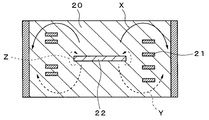
- Patent Documents 1 and 2 below as shown in FIG. 15, a permanent magnet 22 is arranged inside a coil 21 embedded in a magnetic body 20, and a magnetic flux X excited from the coil 21 is used as a permanent magnet.
- An inductance element has been proposed in which the saturation of the magnetic material is suppressed and the direct current superimposition characteristics are improved by canceling with the reverse bias magnetic flux Y generated by the magnet 22.
- JP 2002-170715 A Japanese Patent Laid-Open No. 3-101106
- the present invention has been made in view of the above circumstances, and the DC superposition characteristics can be greatly improved by a permanent magnet that generates a bias magnetic flux. As a result, a low-loss material can be used as a magnetic material. It is an object of the present invention to provide a multilayer inductor capable of improving the converter conversion efficiency.
- the invention according to claim 1 is characterized in that a plurality of electrically insulating magnetic layers and conductive patterns are stacked, and each of the conductive patterns is sequentially connected in the stacking direction to thereby form the magnetic layer.
- the coil is disposed between the outer peripheral edge of the multilayer inductor and the outer peripheral edge of the coil.
- An annular permanent magnet layer magnetized so as to emit a magnetic flux in a direction opposite to the direction of the magnetic flux excited by the inner circumference of the coil in the axial direction view without overlapping the conductive pattern, and It arrange
- a plurality of electrically insulating magnetic layers and conductive patterns are stacked, and each of the conductive patterns is sequentially connected in the stacking direction so as to spiral around the magnetic layer.
- the magnetic flux is magnetized so as to emit a magnetic flux in a direction opposite to the direction of the magnetic flux excited by the coil over the entire inner surface of the coil.
- the annular permanent magnet layer is arranged so that its outer peripheral portion does not overlap with the conductive pattern and closes between the conductive pattern when viewed in the axial direction of the coil. is there.
- a gap is formed between the permanent magnet layer and the conductive pattern in the axial direction view. Is closed by an annular electrically insulating nonmagnetic pattern interposed between the permanent magnet layer and the conductive pattern.
- the invention according to claim 4 is the invention according to any one of claims 1 to 3, wherein the magnetic layer and the permanent magnet layer, or the magnetic layer and the permanent magnet layer, and the nonmagnetic pattern are: It is made of a material that can be collectively baked at a temperature of 940 ° C. or lower.
- the invention described in claim 5 uses a Ni—Zn ferrite material as the magnetic layer, a Zn ferrite material as the nonmagnetic pattern, and Ba as the permanent magnet layer.
- a low-temperature sintered magnet material obtained by adding Bi 2 O 3 and SiO 2 to ferrite powder or Sr ferrite powder is used.
- the permanent magnet layer is disposed on the entire surface outside the coil or inside the coil in the axial direction, it is like the permanent magnet shown in FIG.
- the reverse leakage magnetic flux Z that does not act as the bias magnetic flux Y does not occur.
- the DC superposition characteristics can be greatly improved by the permanent magnet layer.
- a magnetic material (magnetic layer) that is relatively easily saturated but has a low loss can be used, it is possible to improve converter conversion efficiency.
- the laminate can be heated at a temperature of 940 ° C. or lower. It can be easily manufactured by magnetizing the permanent magnet layer after integration by low-temperature sintering.
- Ni—Zn ferrite material is used as the magnetic layer
- Zn ferrite material is used as the nonmagnetic pattern
- Ba ferrite powder is used as the permanent magnet layer.
- FIG. 1 is an overall perspective view showing a first embodiment of the multilayer inductor of the present invention.
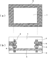
- FIG. 2 is an exploded perspective view showing a multilayer body for manufacturing the multilayer inductor of FIG. 3A and 3B show the multilayer inductor of FIG. 1, in which FIG. 3A is a plan sectional view and FIG. 3B is a longitudinal sectional view.
- FIG. 4 is a longitudinal sectional view of a main part showing a first modification of the first embodiment.
- FIG. 5 is a longitudinal sectional view showing a second modification. 6A and 6B show a third modified example, in which FIG. 6A is a plan sectional view and FIG. 6B is a longitudinal sectional view.
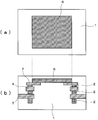
- FIG. 7A and 7B show a second embodiment of the multilayer inductor of the present invention, in which FIG. 7A is a plan sectional view and FIG. 7B is a longitudinal sectional view.
- FIG. 8 shows a first modification of the second embodiment, in which (a) is a plan sectional view and (b) is a longitudinal sectional view.
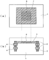
- FIG. 9 shows a second modification of the second embodiment, in which (a) is a plan sectional view and (b) is a longitudinal sectional view.
- FIG. 10 shows a third modification of the second embodiment, where (a) is a plan sectional view and (b) is a longitudinal sectional view.
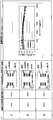
- FIG. 11 is a diagram illustrating the results of an example in which the DC superimposition characteristics of the multilayer inductor shown in the first embodiment and the multilayer inductor of the comparative example are compared.
- FIG. 12 is a diagram illustrating a result of an example in which direct current superposition characteristics of the multilayer inductor illustrated in the second embodiment and the multilayer inductor of the comparative example are compared.
- FIG. 13 is a diagram showing results of an example in which the DC superposition characteristics of the multilayer inductor shown in the first embodiment and a multilayer inductor of a comparative example in which a permanent magnet and an internal conductor are overlapped are compared.
- FIG. 12 is a diagram illustrating a result of an example in which direct current superposition characteristics of the multilayer inductor illustrated in the second embodiment and the multilayer inductor of the comparative example are compared.
- FIG. 13 is a diagram showing results of an example in which the DC superposition characteristics of the multilayer inductor shown in the first embodiment and
- FIG. 14 is a diagram illustrating the results of an example in which the DC superposition characteristics of the multilayer inductor shown in the second embodiment and the multilayer inductor of a comparative example in which a permanent magnet and an internal conductor are overlapped are compared.
- FIG. 15 is a longitudinal sectional view showing a conventional laminated inductor with magnets.
- FIG. 1 to 3 show a first embodiment of a multilayer inductor according to the present invention
- FIGS. 4 to 6 show first to third modifications thereof, respectively.
- this multilayer inductor has a plurality of electrically insulating magnetic layers 1 and conductive patterns 2 stacked, and the conductive patterns 2 of each layer are sequentially connected in the stacking direction, whereby a magnetic layer A coil 2 that spirally circulates in the magnetic body constituted by 1 and is formed in a rectangular parallelepiped shape in which both end portions of the coil 2 are drawn out to the outer peripheral portion and connected to the external electrode 3. It is surface-mounted by being connected to a land portion of a circuit board (not shown).
- an electrically insulating nonmagnetic pattern 4 having a shape corresponding to the shape of the conductive pattern 2 is disposed, and further, a nonmagnetic pattern is disposed at an intermediate position in the stacking direction.
- an electrically insulating nonmagnetic layer 5 serving as a magnetic gap is disposed over the entire surface.
- the outer peripheral edge portion of the multilayer inductor that is, the outer peripheral edge portion of the magnetic layer 1 and the coil 2 when viewed in the axial direction of the coil 2.
- a permanent magnet layer 6 that is magnetized so as to emit a magnetic flux in a direction opposite to the direction of the magnetic flux excited by the coil 2 is disposed over the entire surface between the outer peripheral edge portion and the outer peripheral edge portion.
- the annular permanent magnet layers 6 are respectively disposed adjacent to the upper and lower sides of the conductive pattern 2 located at both ends in the stacking direction. Further, the permanent magnet layer 6 is formed so that its inner dimension is the same as the outer dimension of the conductive pattern 2 so as not to overlap with the coil 2 when viewed in the axial direction.
- a magnetic layer is formed by printing a Ni—Zn based ferrite material paste as an electrical insulating material by a screen printing method or the like. 1 is formed, and a permanent magnet layer 6 is formed on the magnetic layer 1 by printing a low-temperature sintered magnet material paste obtained by adding Bi 2 O 3 or SiO 2 to Ba ferrite powder or Sr ferrite powder.
- the magnetic layer 1 is printed on the portion excluding the permanent magnet layer 6.
- FIG. 2 shows a case where four laminated inductors are simultaneously manufactured on one plane.
- the conductive pattern 2 is printed on the layer on which the permanent magnet layer 6 is formed, and the magnetic layer 1 is similarly printed on a portion excluding the conductive pattern 2.
- the non-magnetic pattern 4 is formed by printing an electrically insulating Zn ferrite material in a shape corresponding to the shape 2, and the magnetic layer 2 is formed in a portion other than the nonmagnetic pattern 4.
- the conductive pattern 2 and the nonmagnetic pattern 4 are alternately stacked in the magnetic layer 1, and the permanent magnet layers 6 are disposed at both ends in the stacking direction.
- the same electrically insulating Zn ferrite material pace as the nonmagnetic pattern 4 is printed over the entire surface to form the nonmagnetic layer 5.
- the upper and lower conductor patterns 2 are electrically connected using via holes or the like.
- the obtained laminate is integrated by firing at a temperature of 940 ° C. or less, specifically about 900 ° C., and then the permanent magnet layer 6 is in a direction opposite to the direction of the magnetic flux excited by the coil 2.
- the multilayer inductor shown in FIG. 1 can be manufactured by magnetizing the magnetic flux so as to be generated.
- each laminated body is sintered after being cut into four laminated bodies constituting each laminated inductor.
- FIG. 4 shows a first modification of the present embodiment.
- This laminated inductor is different from those shown in FIGS. 1 to 3 in that the permanent magnet layer 6 and the conductive pattern 2 in the lamination direction are In other words, a nonmagnetic pattern 7 made of a Zn ferrite material similar to the nonmagnetic pattern 4 formed between the conductive patterns 2 is formed.
- the nonmagnetic pattern 7 is formed when the inner dimension of the permanent magnet layer 6 is the same as the outer dimension of the conductive pattern 2 or between the permanent magnet layer 6 and the conductive pattern 2 in the axial direction view. When the gap is formed in the gap, the dimension is formed so as to close the gap.
- FIG. 5 shows a second modification of the present embodiment.
- This multilayer inductor is a nonmagnetic pattern that is disposed between the conductive patterns 2 and used as an insulating layer in the first embodiment. 4, a magnetic layer 8 having a permeability of 1 ⁇ 4 or less of the magnetic permeability of the magnetic material is disposed over the entire surface between the conductive patterns 2.
- FIG. 6 shows a third modification of the present embodiment.
- the permanent magnet layer 6 is disposed over the entire surface between the outer peripheral edge of the multilayer inductor (that is, the outer peripheral edge of the magnetic layer 1) and the outer peripheral edge of the coil 2.
- the permanent magnet layer 6 is disposed in a layer in which the nonmagnetic pattern 4 is formed and a layer in which the conductive pattern 2 is formed adjacently below the layer.
- the permanent magnet layer 6 is formed so that the inner peripheral edge thereof is in contact with the outer peripheral edge of the nonmagnetic pattern 4 and in the layer in which the conductive pattern 2 is formed. Is formed so that the inner peripheral edge thereof is in contact with the outer peripheral edge of the conductive pattern 2.
- FIG. 7 shows a second embodiment of the multilayer inductor according to the present invention
- FIGS. 8 to 10 show first to third modifications thereof.
- the same components as those shown in FIGS. 1 to 6 are denoted by the same reference numerals, and the description thereof will be simplified.
- the permanent magnet layer 6 magnetized so as to emit a magnetic flux in a direction opposite to the direction of the magnetic flux excited by the coil 2 over the entire inner surface of the coil 2 when viewed in the axial direction of the coil 2. Has been placed.
- An annular nonmagnetic pattern 7 made of a Zn ferrite material is formed so as to extend into the coil 2, and a rectangular permanent magnet layer 6 is disposed on the upper layer of the nonmagnetic pattern 7.
- the permanent magnet layer 6 is formed so that its outer dimension is the same as the inner dimension of the conductive pattern 2 so as not to overlap with the coil 2 in the axial direction view.
- FIG. 8 shows a first modification of the multilayer inductor having the above configuration.
- this multilayer inductor in addition to the permanent magnet 6, the lower side of the lowermost conductive pattern 2 in the drawing in the stacking direction is shown.
- a similar annular nonmagnetic pattern 7 is formed so as to extend into the coil 2, and a rectangular permanent magnet layer 6 is disposed below the nonmagnetic pattern 7.
- the permanent magnet layer 6 is also formed so that its outer dimension is the same as the inner dimension of the conductive pattern 2 so as not to overlap with the coil 2 when viewed in the axial direction.
- FIG. 9 shows a second modification.
- a rectangular permanent magnet layer 6 is disposed inside the uppermost conductive pattern 2 in the diagram in the stacking direction.
- the permanent magnet layer 6 is formed in the same layer as the conductive pattern 2, and its outer dimension is the conductive pattern 2 so as not to overlap with the coil 2 in the axial direction view and not to form a gap. It is formed to be the same as the internal dimensions of
- the outer dimension of the permanent magnet layer 6 shown in FIG. 9 is formed in a square shape smaller than the inner dimension of the conductive pattern 2.
- an annular nonmagnetic pattern 7 is formed between the conductive pattern 2 and the permanent magnet layer 6 so as to close the coil 2 when viewed in the axial direction.
- the permanent magnet layer 6 is closed outside the coil 2 or inside the coil 2 when viewed in the axial direction. Therefore, unlike the permanent magnet shown in FIG. 15, the reverse leakage magnetic flux Z that does not act as the bias magnetic flux Y is not generated. As a result, the DC superposition characteristics can be greatly improved by the permanent magnet layer 6. In other words, since the magnetic body (magnetic layer) 1 can be made of a material that is relatively easily saturated but has low loss, it is possible to improve the converter conversion efficiency.
- a Ni—Zn ferrite material is used as the magnetic layer 1
- a Zn ferrite material is used as the nonmagnetic patterns 4 and 7
- Bi 2 O 3 and SiO are added to the Ba ferrite powder or Sr ferrite powder as the permanent magnet layer 6. Since the low-temperature sintered magnet material to which 2 is added is used, it can be easily manufactured by magnetizing the permanent magnet layer 6 after firing at a temperature of about 900 ° C. at the time of manufacture.
- the DC superposition characteristics of the multilayer inductor of the present invention and the multilayer inductor of the comparative example were obtained and compared by simulation.
- the chip size is 2.5 ⁇ 2.0 ⁇ 1.0 mm
- the number of turns of the internal conductor is 5 turns
- the thickness of the internal conductor is 120 ⁇ m
- the space between the internal conductors The insulating layer thickness was 15 ⁇ m.
- a gap of 50 ⁇ m is formed between the multilayer inductors (1) and (2) having the configurations shown in the first embodiment and the first modification, and the permanent magnet layer and the internal conductor.
- This is a comparison of DC superposition characteristics with the multilayer inductor (3) of the comparative example.
- the multilayer inductor (1) arranged so that the permanent magnet layer and the internal conductor are in contact with each other in the axial direction is more direct current superimposed characteristics than the multilayer inductor (3) of the comparative example. Excellent.
- the DC superimposition characteristics equivalent to those of the multilayer inductor (1) are provided. Is obtained.
- FIG. 12 shows the multilayer inductors (4) and (5) having the configurations shown in the second and third modifications of the second embodiment, the inner conductor, and the permanent magnet disposed therein.
- the direct current superposition characteristics are compared with those of the multilayer inductor (6) of the comparative example in which a gap of 50 ⁇ m is formed.
- the multilayer inductors (4) and (5) according to the present invention are superior in characteristics to the multilayer inductor (6) of the comparative example.
- FIG. 13 compares the DC superimposition characteristics of the multilayer inductor (1) with the multilayer inductor (7) of the comparative example in which the permanent magnet layer and the internal conductor are overlapped by 150 ⁇ m in the axial direction of the coil. It is. From the figure, it can be seen that the direct current superimposition characteristics of the multilayer inductor (7) of the comparative example in which the permanent magnet layer and the internal conductor are overlapped with the multilayer inductor (1) according to the present invention are significantly deteriorated.
- FIG. 14 shows a DC superposition of the multilayer inductor (4) and the multilayer inductor (8) of the comparative example in which the permanent magnet layer disposed in the inner conductor and the inner conductor are overlapped by 150 ⁇ m in the axial direction of the coil. It is a comparison of characteristics.
- FIG. 13 shows that the multilayer inductor (8) of the comparative example in which the permanent magnet layer and the internal conductor overlap with the multilayer inductor (4) according to the present invention has a particularly large decrease in the initial value. Similar to the results shown, it can be seen that the structure in which the permanent magnet layer is overlaid on the inner conductor in the axial direction is not preferable.
- a permanent magnet that generates a bias magnetic flux can provide a multilayer inductor that can greatly improve the DC superposition characteristics, and that can use a low-loss material as a magnetic material to improve converter conversion efficiency. .
- Magnetic layer 2 Conductive pattern (coil) 3 External electrode 4, 5, 7, 8 Nonmagnetic pattern 6 Permanent magnet layer
Landscapes
- Engineering & Computer Science (AREA)
- Power Engineering (AREA)
- Microelectronics & Electronic Packaging (AREA)
- Coils Or Transformers For Communication (AREA)
- Manufacturing Cores, Coils, And Magnets (AREA)
Abstract
Description
しかしながら、一般的に上記フェライトは、磁束飽和密度が低く、直流重畳特性が悪い傾向があるために、昨今のモバイル市場における電流増加に追従することが困難になりつつある。
図1~図3は、本発明に係る積層インダクタの第1の実施形態を示すものであり、図4~図6は、各々その第1~第3の変形例を示すものである。
図1~図3に示すように、この積層インダクタは、複数の電気絶縁性の磁性層1および導電パターン2が積層され、各層の導電パターン2が積層方向に順次接続されることにより、磁性層1によって構成される磁性体内において螺旋状に周回するコイル2が形成されるとともに、コイル2の両端部が外周部に引き出されて外部電極3に接続された直方体状のもので、外部電極3が図示されない回路基板のランド部に接続されることにより、面実装されるものである。
なお、図2は、一平面に4個の積層インダクタを同時に製造する場合を示すものである。
この積層インダクタにおいては、積層インダクタの外周縁部(すなわち磁性層1の外周縁部)とコイル2の外周縁部との間の全面に、2層にわたって永久磁石層6が配置されている。ここで、永久磁石層6は、非磁性パターン4が形成されている層と、その下方に隣接して導電パターン2が形成されている層とに配置されている。
図7は、本発明に係る積層インダクタの第2の実施形態を示すものであり、図8~図10は、その第1~第3の変形例を示すものである。なお、以下、図1~図6に示したものと同一構成部分については、同一符号を付してその説明を簡略化する。
これらの積層インダクタにおいては、コイル2の軸線方向視において、コイル2の内部の全面にわたって、コイル2によって励磁される磁束の方向と逆方向の磁束を発するように着磁された永久磁石層6が配置されている。
なお、本発明の積層インダクタおよび比較例の積層インダクタ共に、チップサイズは2.5×2.0×1.0mm、内部導体の巻数は5ターン、内部導体の膜厚は120μm、内部導体間の絶縁層厚さは15μmとした。
2 導電パターン(コイル)
3 外部電極
4、5、7、8 非磁性パターン
6 永久磁石層
Claims (5)
- 複数の電気絶縁性の磁性層および導電パターンが積層され、各々の上記導電パターンが上記積層方向に順次接続されることにより上記磁性層内に螺旋状に周回するコイルが形成されるとともに、上記コイルの両端部が外周部に引き出される積層インダクタにおいて、
上記積層インダクタの外周縁部と上記コイルの外周縁部との間に、上記コイルによって励磁される磁束の方向と逆方向の磁束を発するように着磁された環状の永久磁石層を、上記コイルの軸線方向視において、その内周部が上記導電パターンと重複することなく、かつ上記導電パターンとの間を塞ぐように配置したことを特徴とする積層インダクタ。 - 複数の電気絶縁性の磁性層および導電パターンが積層され、各々の上記導電パターンが上記積層方向に順次接続されることにより上記磁性層内に螺旋状に周回するコイルが形成されるとともに、上記コイルの両端部が外周部に引き出される積層インダクタにおいて、
上記コイルの内部の全面にわたって、上記コイルによって励磁される磁束の方向と逆方向の磁束を発するように着磁された環状の永久磁石層を、上記コイルの軸線方向視において、その外周部が上記導電パターンと重複することなく、かつ上記導電パターンとの間を塞ぐように配置したことを特徴とする積層インダクタ。 - 上記軸線方向視において、上記永久磁石層と上記導電パターンとの間に間隙が形成されているとともに、当該間隙が上記永久磁石層と上記導電パターンとの間に介装された環状の電気絶縁性の非磁性パターンとによって塞がれていることを特徴とする請求項1または2に記載の積層インダクタ。
- 上記磁性層および上記永久磁石層、または上記磁性層および上記永久磁石層並びに上記非磁性パターンは、940℃以下の温度で一括焼成可能な材料からなることを特徴とする請求項1ないし3のいずれかに記載の積層インダクタ。
- 上記磁性層としてNi-Znフェライト系材料を用い、上記非磁性パターンとしてZnフェライト系材料を用い、上記永久磁石層としてBaフェライト粉体またはSrフェライト粉体にBi2O3およびSiO2を添加した低温焼結磁石材料を用いたことを特徴とする請求項4に記載の積層インダクタ。
Priority Applications (3)
| Application Number | Priority Date | Filing Date | Title |
|---|---|---|---|
| CN201480034887.4A CN105308694B (zh) | 2013-06-19 | 2014-05-16 | 层叠电感器 |
| KR1020157031588A KR102030086B1 (ko) | 2013-06-19 | 2014-05-16 | 적층 인덕터 |
| US14/898,587 US9653203B2 (en) | 2013-06-19 | 2014-05-16 | Multilayer inductor |
Applications Claiming Priority (2)
| Application Number | Priority Date | Filing Date | Title |
|---|---|---|---|
| JP2013-128372 | 2013-06-19 | ||
| JP2013128372A JP6295403B2 (ja) | 2013-06-19 | 2013-06-19 | 積層インダクタ |
Publications (1)
| Publication Number | Publication Date |
|---|---|
| WO2014203447A1 true WO2014203447A1 (ja) | 2014-12-24 |
Family
ID=52104201
Family Applications (1)
| Application Number | Title | Priority Date | Filing Date |
|---|---|---|---|
| PCT/JP2014/002577 Ceased WO2014203447A1 (ja) | 2013-06-19 | 2014-05-16 | 積層インダクタ |
Country Status (5)
| Country | Link |
|---|---|
| US (1) | US9653203B2 (ja) |
| JP (1) | JP6295403B2 (ja) |
| KR (1) | KR102030086B1 (ja) |
| CN (1) | CN105308694B (ja) |
| WO (1) | WO2014203447A1 (ja) |
Cited By (1)
| Publication number | Priority date | Publication date | Assignee | Title |
|---|---|---|---|---|
| CN105428034A (zh) * | 2015-12-09 | 2016-03-23 | 浙江师范大学 | 一种底层埋入式微米级三维薄膜电感器及其制造方法 |
Families Citing this family (2)
| Publication number | Priority date | Publication date | Assignee | Title |
|---|---|---|---|---|
| JP6313094B2 (ja) * | 2014-04-01 | 2018-04-18 | Fdk株式会社 | 積層インダクタ |
| JP6574574B6 (ja) * | 2015-01-21 | 2020-01-15 | Njコンポーネント株式会社 | 積層インダクタ |
Citations (4)
| Publication number | Priority date | Publication date | Assignee | Title |
|---|---|---|---|---|
| JPH0281410A (ja) * | 1988-09-17 | 1990-03-22 | Toko Inc | 電流制御型積層インダクタ |
| JP2002175927A (ja) * | 2000-12-08 | 2002-06-21 | Tokin Corp | 積層インダクタンス素子及びその製造方法 |
| JP2002175917A (ja) * | 2000-12-08 | 2002-06-21 | Tokin Corp | 積層インダクタおよびその製造方法 |
| JP2006196591A (ja) * | 2005-01-12 | 2006-07-27 | Fdk Corp | 積層インダクタ |
Family Cites Families (5)
| Publication number | Priority date | Publication date | Assignee | Title |
|---|---|---|---|---|
| JPH03101106A (ja) | 1989-09-13 | 1991-04-25 | Tdk Corp | インダクタンス素子 |
| JP2002170715A (ja) | 2000-12-01 | 2002-06-14 | Tokin Corp | インダクタンス素子及びその製造方法 |
| CA2753895C (en) * | 2006-10-30 | 2013-12-10 | Gambro Lundia Ab | Air separator for extracorporeal fluid treatment sets |
| CN101814485B (zh) * | 2009-02-23 | 2012-08-22 | 万国半导体股份有限公司 | 具堆栈式电感和ic芯片的小型功率半导体封装及方法 |
| JP5581975B2 (ja) * | 2010-07-07 | 2014-09-03 | ソニー株式会社 | 通信制御装置、通信制御方法、通信システム及び通信装置 |
-
2013
- 2013-06-19 JP JP2013128372A patent/JP6295403B2/ja active Active
-
2014
- 2014-05-16 US US14/898,587 patent/US9653203B2/en active Active
- 2014-05-16 WO PCT/JP2014/002577 patent/WO2014203447A1/ja not_active Ceased
- 2014-05-16 CN CN201480034887.4A patent/CN105308694B/zh active Active
- 2014-05-16 KR KR1020157031588A patent/KR102030086B1/ko active Active
Patent Citations (4)
| Publication number | Priority date | Publication date | Assignee | Title |
|---|---|---|---|---|
| JPH0281410A (ja) * | 1988-09-17 | 1990-03-22 | Toko Inc | 電流制御型積層インダクタ |
| JP2002175927A (ja) * | 2000-12-08 | 2002-06-21 | Tokin Corp | 積層インダクタンス素子及びその製造方法 |
| JP2002175917A (ja) * | 2000-12-08 | 2002-06-21 | Tokin Corp | 積層インダクタおよびその製造方法 |
| JP2006196591A (ja) * | 2005-01-12 | 2006-07-27 | Fdk Corp | 積層インダクタ |
Cited By (2)
| Publication number | Priority date | Publication date | Assignee | Title |
|---|---|---|---|---|
| CN105428034A (zh) * | 2015-12-09 | 2016-03-23 | 浙江师范大学 | 一种底层埋入式微米级三维薄膜电感器及其制造方法 |
| CN105428034B (zh) * | 2015-12-09 | 2018-03-30 | 浙江师范大学 | 一种底层埋入式微米级三维薄膜电感器及其制造方法 |
Also Published As
| Publication number | Publication date |
|---|---|
| CN105308694A (zh) | 2016-02-03 |
| JP2015005548A (ja) | 2015-01-08 |
| KR102030086B1 (ko) | 2019-10-08 |
| US9653203B2 (en) | 2017-05-16 |
| JP6295403B2 (ja) | 2018-03-20 |
| KR20160021087A (ko) | 2016-02-24 |
| CN105308694B (zh) | 2018-03-30 |
| US20160141089A1 (en) | 2016-05-19 |
Similar Documents
| Publication | Publication Date | Title |
|---|---|---|
| JP3621300B2 (ja) | 電源回路用積層インダクタ | |
| KR101862401B1 (ko) | 적층형 인덕터 및 그 제조방법 | |
| KR101853135B1 (ko) | 적층형 파워인덕터 및 이의 제조 방법 | |
| JPWO2017014065A1 (ja) | 積層インダクタ及び積層インダクタ製造方法 | |
| JP2001044037A (ja) | 積層インダクタ | |
| WO2005010901A2 (ja) | 磁心型積層インダクタ | |
| JP2013140958A (ja) | 積層型インダクタ | |
| WO2008007705A1 (fr) | Inducteur multicouche | |
| JP4873522B2 (ja) | 積層インダクタ | |
| JP2014187276A (ja) | 積層インダクタ | |
| JP6295403B2 (ja) | 積層インダクタ | |
| KR101214731B1 (ko) | 적층형 인덕터 및 이의 제조 방법 | |
| KR101853129B1 (ko) | 적층형 파워인덕터 | |
| KR100843422B1 (ko) | 적층형 인덕터 | |
| JP2013065853A (ja) | 積層型インダクタ及びその製造方法 | |
| JP4716308B2 (ja) | 積層インダクタ | |
| KR100770249B1 (ko) | 적층코일 | |
| JP6313094B2 (ja) | 積層インダクタ | |
| JP2007324554A (ja) | 積層インダクタ | |
| JP2007317892A (ja) | 積層インダクタ | |
| JP4827087B2 (ja) | 積層インダクタ | |
| KR20150006678A (ko) | 적층형 인덕터 및 이의 제조방법 | |
| KR20120045949A (ko) | 적층형 인덕터 및 그 제조방법 | |
| KR101228667B1 (ko) | 적층 세라믹 전자 부품 | |
| KR20130031083A (ko) | 적층형 인덕터 |
Legal Events
| Date | Code | Title | Description |
|---|---|---|---|
| WWE | Wipo information: entry into national phase |
Ref document number: 201480034887.4 Country of ref document: CN |
|
| 121 | Ep: the epo has been informed by wipo that ep was designated in this application |
Ref document number: 14814174 Country of ref document: EP Kind code of ref document: A1 |
|
| ENP | Entry into the national phase |
Ref document number: 20157031588 Country of ref document: KR Kind code of ref document: A |
|
| WWE | Wipo information: entry into national phase |
Ref document number: 14898587 Country of ref document: US |
|
| NENP | Non-entry into the national phase |
Ref country code: DE |
|
| 122 | Ep: pct application non-entry in european phase |
Ref document number: 14814174 Country of ref document: EP Kind code of ref document: A1 |