WO2014199677A1 - 表示装置 - Google Patents
表示装置 Download PDFInfo
- Publication number
- WO2014199677A1 WO2014199677A1 PCT/JP2014/055372 JP2014055372W WO2014199677A1 WO 2014199677 A1 WO2014199677 A1 WO 2014199677A1 JP 2014055372 W JP2014055372 W JP 2014055372W WO 2014199677 A1 WO2014199677 A1 WO 2014199677A1
- Authority
- WO
- WIPO (PCT)
- Prior art keywords
- pixel
- electrode portion
- tft
- resistive
- wiring
- Prior art date
- Legal status (The legal status is an assumption and is not a legal conclusion. Google has not performed a legal analysis and makes no representation as to the accuracy of the status listed.)
- Ceased
Links
Images












Classifications
-
- G—PHYSICS
- G02—OPTICS
- G02F—OPTICAL DEVICES OR ARRANGEMENTS FOR THE CONTROL OF LIGHT BY MODIFICATION OF THE OPTICAL PROPERTIES OF THE MEDIA OF THE ELEMENTS INVOLVED THEREIN; NON-LINEAR OPTICS; FREQUENCY-CHANGING OF LIGHT; OPTICAL LOGIC ELEMENTS; OPTICAL ANALOGUE/DIGITAL CONVERTERS
- G02F1/00—Devices or arrangements for the control of the intensity, colour, phase, polarisation or direction of light arriving from an independent light source, e.g. switching, gating or modulating; Non-linear optics
- G02F1/01—Devices or arrangements for the control of the intensity, colour, phase, polarisation or direction of light arriving from an independent light source, e.g. switching, gating or modulating; Non-linear optics for the control of the intensity, phase, polarisation or colour
- G02F1/13—Devices or arrangements for the control of the intensity, colour, phase, polarisation or direction of light arriving from an independent light source, e.g. switching, gating or modulating; Non-linear optics for the control of the intensity, phase, polarisation or colour based on liquid crystals, e.g. single liquid crystal display cells
- G02F1/133—Constructional arrangements; Operation of liquid crystal cells; Circuit arrangements
- G02F1/1333—Constructional arrangements; Manufacturing methods
- G02F1/1335—Structural association of cells with optical devices, e.g. polarisers or reflectors
- G02F1/133509—Filters, e.g. light shielding masks
- G02F1/133514—Colour filters
-
- G—PHYSICS
- G02—OPTICS
- G02F—OPTICAL DEVICES OR ARRANGEMENTS FOR THE CONTROL OF LIGHT BY MODIFICATION OF THE OPTICAL PROPERTIES OF THE MEDIA OF THE ELEMENTS INVOLVED THEREIN; NON-LINEAR OPTICS; FREQUENCY-CHANGING OF LIGHT; OPTICAL LOGIC ELEMENTS; OPTICAL ANALOGUE/DIGITAL CONVERTERS
- G02F1/00—Devices or arrangements for the control of the intensity, colour, phase, polarisation or direction of light arriving from an independent light source, e.g. switching, gating or modulating; Non-linear optics
- G02F1/01—Devices or arrangements for the control of the intensity, colour, phase, polarisation or direction of light arriving from an independent light source, e.g. switching, gating or modulating; Non-linear optics for the control of the intensity, phase, polarisation or colour
- G02F1/13—Devices or arrangements for the control of the intensity, colour, phase, polarisation or direction of light arriving from an independent light source, e.g. switching, gating or modulating; Non-linear optics for the control of the intensity, phase, polarisation or colour based on liquid crystals, e.g. single liquid crystal display cells
- G02F1/133—Constructional arrangements; Operation of liquid crystal cells; Circuit arrangements
- G02F1/136—Liquid crystal cells structurally associated with a semi-conducting layer or substrate, e.g. cells forming part of an integrated circuit
- G02F1/1362—Active matrix addressed cells
- G02F1/136213—Storage capacitors associated with the pixel electrode
-
- G—PHYSICS
- G02—OPTICS
- G02F—OPTICAL DEVICES OR ARRANGEMENTS FOR THE CONTROL OF LIGHT BY MODIFICATION OF THE OPTICAL PROPERTIES OF THE MEDIA OF THE ELEMENTS INVOLVED THEREIN; NON-LINEAR OPTICS; FREQUENCY-CHANGING OF LIGHT; OPTICAL LOGIC ELEMENTS; OPTICAL ANALOGUE/DIGITAL CONVERTERS
- G02F1/00—Devices or arrangements for the control of the intensity, colour, phase, polarisation or direction of light arriving from an independent light source, e.g. switching, gating or modulating; Non-linear optics
- G02F1/01—Devices or arrangements for the control of the intensity, colour, phase, polarisation or direction of light arriving from an independent light source, e.g. switching, gating or modulating; Non-linear optics for the control of the intensity, phase, polarisation or colour
- G02F1/13—Devices or arrangements for the control of the intensity, colour, phase, polarisation or direction of light arriving from an independent light source, e.g. switching, gating or modulating; Non-linear optics for the control of the intensity, phase, polarisation or colour based on liquid crystals, e.g. single liquid crystal display cells
- G02F1/133—Constructional arrangements; Operation of liquid crystal cells; Circuit arrangements
- G02F1/136—Liquid crystal cells structurally associated with a semi-conducting layer or substrate, e.g. cells forming part of an integrated circuit
- G02F1/1362—Active matrix addressed cells
- G02F1/136286—Wiring, e.g. gate line, drain line
-
- G—PHYSICS
- G02—OPTICS
- G02F—OPTICAL DEVICES OR ARRANGEMENTS FOR THE CONTROL OF LIGHT BY MODIFICATION OF THE OPTICAL PROPERTIES OF THE MEDIA OF THE ELEMENTS INVOLVED THEREIN; NON-LINEAR OPTICS; FREQUENCY-CHANGING OF LIGHT; OPTICAL LOGIC ELEMENTS; OPTICAL ANALOGUE/DIGITAL CONVERTERS
- G02F1/00—Devices or arrangements for the control of the intensity, colour, phase, polarisation or direction of light arriving from an independent light source, e.g. switching, gating or modulating; Non-linear optics
- G02F1/01—Devices or arrangements for the control of the intensity, colour, phase, polarisation or direction of light arriving from an independent light source, e.g. switching, gating or modulating; Non-linear optics for the control of the intensity, phase, polarisation or colour
- G02F1/13—Devices or arrangements for the control of the intensity, colour, phase, polarisation or direction of light arriving from an independent light source, e.g. switching, gating or modulating; Non-linear optics for the control of the intensity, phase, polarisation or colour based on liquid crystals, e.g. single liquid crystal display cells
- G02F1/133—Constructional arrangements; Operation of liquid crystal cells; Circuit arrangements
- G02F1/136—Liquid crystal cells structurally associated with a semi-conducting layer or substrate, e.g. cells forming part of an integrated circuit
- G02F1/1362—Active matrix addressed cells
- G02F1/1368—Active matrix addressed cells in which the switching element is a three-electrode device
-
- G—PHYSICS
- G09—EDUCATION; CRYPTOGRAPHY; DISPLAY; ADVERTISING; SEALS
- G09G—ARRANGEMENTS OR CIRCUITS FOR CONTROL OF INDICATING DEVICES USING STATIC MEANS TO PRESENT VARIABLE INFORMATION
- G09G3/00—Control arrangements or circuits, of interest only in connection with visual indicators other than cathode-ray tubes
- G09G3/20—Control arrangements or circuits, of interest only in connection with visual indicators other than cathode-ray tubes for presentation of an assembly of a number of characters, e.g. a page, by composing the assembly by combination of individual elements arranged in a matrix no fixed position being assigned to or needed to be assigned to the individual characters or partial characters
- G09G3/34—Control arrangements or circuits, of interest only in connection with visual indicators other than cathode-ray tubes for presentation of an assembly of a number of characters, e.g. a page, by composing the assembly by combination of individual elements arranged in a matrix no fixed position being assigned to or needed to be assigned to the individual characters or partial characters by control of light from an independent source
- G09G3/36—Control arrangements or circuits, of interest only in connection with visual indicators other than cathode-ray tubes for presentation of an assembly of a number of characters, e.g. a page, by composing the assembly by combination of individual elements arranged in a matrix no fixed position being assigned to or needed to be assigned to the individual characters or partial characters by control of light from an independent source using liquid crystals
- G09G3/3611—Control of matrices with row and column drivers
- G09G3/3648—Control of matrices with row and column drivers using an active matrix
- G09G3/3655—Details of drivers for counter electrodes, e.g. common electrodes for pixel capacitors or supplementary storage capacitors
-
- G—PHYSICS
- G09—EDUCATION; CRYPTOGRAPHY; DISPLAY; ADVERTISING; SEALS
- G09G—ARRANGEMENTS OR CIRCUITS FOR CONTROL OF INDICATING DEVICES USING STATIC MEANS TO PRESENT VARIABLE INFORMATION
- G09G3/00—Control arrangements or circuits, of interest only in connection with visual indicators other than cathode-ray tubes
- G09G3/20—Control arrangements or circuits, of interest only in connection with visual indicators other than cathode-ray tubes for presentation of an assembly of a number of characters, e.g. a page, by composing the assembly by combination of individual elements arranged in a matrix no fixed position being assigned to or needed to be assigned to the individual characters or partial characters
- G09G3/34—Control arrangements or circuits, of interest only in connection with visual indicators other than cathode-ray tubes for presentation of an assembly of a number of characters, e.g. a page, by composing the assembly by combination of individual elements arranged in a matrix no fixed position being assigned to or needed to be assigned to the individual characters or partial characters by control of light from an independent source
- G09G3/36—Control arrangements or circuits, of interest only in connection with visual indicators other than cathode-ray tubes for presentation of an assembly of a number of characters, e.g. a page, by composing the assembly by combination of individual elements arranged in a matrix no fixed position being assigned to or needed to be assigned to the individual characters or partial characters by control of light from an independent source using liquid crystals
- G09G3/3611—Control of matrices with row and column drivers
- G09G3/3648—Control of matrices with row and column drivers using an active matrix
- G09G3/3659—Control of matrices with row and column drivers using an active matrix the addressing of the pixel involving the control of two or more scan electrodes or two or more data electrodes, e.g. pixel voltage dependant on signal of two data electrodes
-
- H—ELECTRICITY
- H10—SEMICONDUCTOR DEVICES; ELECTRIC SOLID-STATE DEVICES NOT OTHERWISE PROVIDED FOR
- H10D—INORGANIC ELECTRIC SEMICONDUCTOR DEVICES
- H10D86/00—Integrated devices formed in or on insulating or conducting substrates, e.g. formed in silicon-on-insulator [SOI] substrates or on stainless steel or glass substrates
- H10D86/40—Integrated devices formed in or on insulating or conducting substrates, e.g. formed in silicon-on-insulator [SOI] substrates or on stainless steel or glass substrates characterised by multiple TFTs
- H10D86/421—Integrated devices formed in or on insulating or conducting substrates, e.g. formed in silicon-on-insulator [SOI] substrates or on stainless steel or glass substrates characterised by multiple TFTs having a particular composition, shape or crystalline structure of the active layer
- H10D86/423—Integrated devices formed in or on insulating or conducting substrates, e.g. formed in silicon-on-insulator [SOI] substrates or on stainless steel or glass substrates characterised by multiple TFTs having a particular composition, shape or crystalline structure of the active layer comprising semiconductor materials not belonging to the Group IV, e.g. InGaZnO
-
- H—ELECTRICITY
- H10—SEMICONDUCTOR DEVICES; ELECTRIC SOLID-STATE DEVICES NOT OTHERWISE PROVIDED FOR
- H10D—INORGANIC ELECTRIC SEMICONDUCTOR DEVICES
- H10D86/00—Integrated devices formed in or on insulating or conducting substrates, e.g. formed in silicon-on-insulator [SOI] substrates or on stainless steel or glass substrates
- H10D86/40—Integrated devices formed in or on insulating or conducting substrates, e.g. formed in silicon-on-insulator [SOI] substrates or on stainless steel or glass substrates characterised by multiple TFTs
- H10D86/441—Interconnections, e.g. scanning lines
-
- H—ELECTRICITY
- H10—SEMICONDUCTOR DEVICES; ELECTRIC SOLID-STATE DEVICES NOT OTHERWISE PROVIDED FOR
- H10D—INORGANIC ELECTRIC SEMICONDUCTOR DEVICES
- H10D86/00—Integrated devices formed in or on insulating or conducting substrates, e.g. formed in silicon-on-insulator [SOI] substrates or on stainless steel or glass substrates
- H10D86/40—Integrated devices formed in or on insulating or conducting substrates, e.g. formed in silicon-on-insulator [SOI] substrates or on stainless steel or glass substrates characterised by multiple TFTs
- H10D86/481—Integrated devices formed in or on insulating or conducting substrates, e.g. formed in silicon-on-insulator [SOI] substrates or on stainless steel or glass substrates characterised by multiple TFTs integrated with passive devices, e.g. auxiliary capacitors
-
- H—ELECTRICITY
- H10—SEMICONDUCTOR DEVICES; ELECTRIC SOLID-STATE DEVICES NOT OTHERWISE PROVIDED FOR
- H10D—INORGANIC ELECTRIC SEMICONDUCTOR DEVICES
- H10D86/00—Integrated devices formed in or on insulating or conducting substrates, e.g. formed in silicon-on-insulator [SOI] substrates or on stainless steel or glass substrates
- H10D86/40—Integrated devices formed in or on insulating or conducting substrates, e.g. formed in silicon-on-insulator [SOI] substrates or on stainless steel or glass substrates characterised by multiple TFTs
- H10D86/60—Integrated devices formed in or on insulating or conducting substrates, e.g. formed in silicon-on-insulator [SOI] substrates or on stainless steel or glass substrates characterised by multiple TFTs wherein the TFTs are in active matrices
-
- G—PHYSICS
- G09—EDUCATION; CRYPTOGRAPHY; DISPLAY; ADVERTISING; SEALS
- G09G—ARRANGEMENTS OR CIRCUITS FOR CONTROL OF INDICATING DEVICES USING STATIC MEANS TO PRESENT VARIABLE INFORMATION
- G09G2300/00—Aspects of the constitution of display devices
- G09G2300/04—Structural and physical details of display devices
- G09G2300/0421—Structural details of the set of electrodes
- G09G2300/0426—Layout of electrodes and connections
-
- G—PHYSICS
- G09—EDUCATION; CRYPTOGRAPHY; DISPLAY; ADVERTISING; SEALS
- G09G—ARRANGEMENTS OR CIRCUITS FOR CONTROL OF INDICATING DEVICES USING STATIC MEANS TO PRESENT VARIABLE INFORMATION
- G09G2300/00—Aspects of the constitution of display devices
- G09G2300/08—Active matrix structure, i.e. with use of active elements, inclusive of non-linear two terminal elements, in the pixels together with light emitting or modulating elements
- G09G2300/0809—Several active elements per pixel in active matrix panels
- G09G2300/0842—Several active elements per pixel in active matrix panels forming a memory circuit, e.g. a dynamic memory with one capacitor
- G09G2300/0852—Several active elements per pixel in active matrix panels forming a memory circuit, e.g. a dynamic memory with one capacitor being a dynamic memory with more than one capacitor
-
- G—PHYSICS
- G09—EDUCATION; CRYPTOGRAPHY; DISPLAY; ADVERTISING; SEALS
- G09G—ARRANGEMENTS OR CIRCUITS FOR CONTROL OF INDICATING DEVICES USING STATIC MEANS TO PRESENT VARIABLE INFORMATION
- G09G2320/00—Control of display operating conditions
- G09G2320/02—Improving the quality of display appearance
- G09G2320/0247—Flicker reduction other than flicker reduction circuits used for single beam cathode-ray tubes
-
- G—PHYSICS
- G09—EDUCATION; CRYPTOGRAPHY; DISPLAY; ADVERTISING; SEALS
- G09G—ARRANGEMENTS OR CIRCUITS FOR CONTROL OF INDICATING DEVICES USING STATIC MEANS TO PRESENT VARIABLE INFORMATION
- G09G2380/00—Specific applications
- G09G2380/10—Automotive applications
Definitions
- the present invention relates to a display device.
- a liquid crystal panel used in a liquid crystal display device has a structure in which a liquid crystal layer is sandwiched between a pair of glass substrates.
- One of the glass substrates is an array substrate having TFTs and pixel electrodes as switching elements. Composed.
- This array substrate has a configuration in which gate wirings and source wirings are provided in a grid pattern on the substrate, and TFTs and pixel electrodes are provided at intersections of the gate wirings and the source wirings.
- the off-characteristics of the TFT have been increasing in recent years. Therefore, it is difficult for the charge stored in the pixel electrode to be reduced by natural discharge when charged by the TFT.
- Patent Document 1 A technique described in Patent Document 1 below is known as a technique for preventing such display image from being burned in and flickering.
- Patent Document 1 when the display on the liquid crystal panel is turned off, the TFT is driven to apply a voltage for releasing the charge stored in the pixel electrode. However, this makes it necessary to perform special control such as driving the TFT when the display is turned off.
- the present invention has been completed based on the above-described circumstances, and an object thereof is to suppress a decrease in display quality without performing special control.
- the display device of the present invention includes a pixel portion, a switching element connected to the pixel portion and capable of charging the pixel portion, a reference potential portion to be a reference potential, the pixel portion, and the reference potential portion And a resistive element that constitutes a resistance component against charges moving between the pixel portion and the reference potential portion.
- the above-described pixel portion is connected to the reference potential portion with a resistive element interposed therebetween, for example, when the potential of the pixel portion is higher than the reference potential of the reference potential portion.
- the resistive element constitutes a resistance component against the charge moving between the pixel portion and the reference potential portion, it can gain time until the potential of the pixel portion reaches the reference potential.
- the resistive element includes at least a gate electrode part, a source electrode part, a drain electrode part, and a channel part that connects the source electrode part and the drain electrode part, and A gate electrode portion is connected to either the pixel portion or the reference potential portion, and one of the source electrode portion and the drain electrode portion is the pixel portion, and the other is the reference potential portion.
- the gate electrode portion is set to the same potential as either the pixel portion or the reference potential portion
- one of the source electrode portion and the drain electrode portion is set to the same potential as the pixel portion
- the other is set to the same potential as the reference potential portion.
- the transistor substantially functions as a diode, and charges are transferred between the source electrode portion and the drain electrode portion through the channel portion.
- the transistor is forward-biased or reverse-biased according to the potential charged in the pixel portion by the switching element. In the case of forward-bias, the amount of charge movement is as long as the threshold voltage of the transistor is not exceeded. On the other hand, in the case of reverse bias, only a charge about the leakage current of the transistor flows, and the amount of charge movement is extremely small.
- the transistor since the transistor constitutes a resistance component with respect to the charge moving between the pixel portion and the reference potential portion, it is possible to sufficiently obtain the time until the potential of the pixel portion becomes the reference potential. it can. As a result, when an image is displayed on the display device, a situation in which the display quality related to the display image is impaired is less likely to occur.
- the switching element includes a pixel gate electrode portion, a pixel source electrode portion, a pixel drain electrode portion connected to the pixel portion, the pixel source electrode portion, and the pixel drain electrode portion.
- a pixel channel portion connecting at least a pixel channel portion, and the transistor constituting the resistive element includes the pixel transistor of which the channel portion constitutes the switching element. It is made of the same material as the pixel channel portion. In this case, by sharing the material for the pixel channel portion of the pixel transistor constituting the switching element and the channel portion of the transistor constituting the resistive element, it is possible to reduce the manufacturing cost. Useful.
- the ratio of the length dimension, which is the distance between the source electrode part and the drain electrode part in the channel part, divided by the width dimension is the switching element.
- the pixel transistor of the pixel transistor to be formed is formed to be larger than a ratio obtained by dividing a length dimension, which is a distance between the pixel source electrode section and the pixel drain electrode section, by a width dimension in the pixel channel section. ing. According to this configuration, the resistance value related to the charge that moves between the source electrode portion and the drain electrode portion via the channel portion in the transistor that constitutes the resistive element is reduced in the pixel transistor that constitutes the switching element.
- the resistance value is larger than the resistance value related to the charge moving between the pixel source electrode portion and the pixel drain electrode portion via the channel portion.
- the gate electrode portion and the source electrode portion are connected to the pixel portion, and the drain electrode portion is connected to the reference potential portion.
- the transistors constituting the resistive element are forward-biased, so that the potential of the gate electrode portion is the same.
- the charge moves from the source electrode portion (pixel portion) to the drain electrode portion (reference potential portion).
- the transistor constituting the resistive element is reverse-biased, so that the drain electrode portion (reference potential portion) is changed to the gate electrode portion.
- the charge moves to the source electrode portion (pixel portion) having the same potential as that of the first electrode portion.
- the transistor since the transistor constitutes a resistance component with respect to the charge moving between the pixel portion and the reference potential portion, it is possible to sufficiently obtain the time until the potential of the pixel portion becomes the reference potential. it can. As a result, when an image is displayed on the display device, a situation in which the display quality related to the display image is impaired is less likely to occur.
- the drain electrode portion is connected to the pixel portion, and the gate electrode portion and the source electrode portion are connected to the reference potential portion.
- the transistor constituting the resistive element is reverse-biased, so that the drain electrode portion (pixel portion) The charge moves to the source electrode portion (reference potential portion) that has the same potential as the gate electrode portion.
- the transistor constituting the resistive element is forward-biased, so that the source electrode portion having the same potential as the gate electrode portion The charge moves from the (reference potential portion) to the drain electrode portion (pixel portion).
- the transistor since the transistor constitutes a resistance component with respect to the charge moving between the pixel portion and the reference potential portion, it is possible to sufficiently obtain the time until the potential of the pixel portion becomes the reference potential. it can. As a result, when an image is displayed on the display device, a situation in which the display quality related to the display image is impaired is less likely to occur.
- the transistor constituting the resistive element includes a first gate electrode portion, a first source electrode portion, a first drain electrode portion, the first source electrode portion, and the first drain electrode portion.
- the first transistor when the potential of the pixel portion is higher than the reference potential of the reference potential portion, the first transistor is forward biased, but the second transistor is reverse biased, and the charge of the pixel portion is Is moved from the first source electrode portion having the same potential as the first gate electrode portion to the first drain electrode portion, and then the second source having the same potential as the second gate electrode portion from the second drain electrode portion.
- the reference potential portion is reached by moving to the electrode portion.
- the second transistor when the potential of the pixel portion is lower than the reference potential of the reference potential portion, the second transistor is forward biased, but the first transistor is reverse biased, and the charge of the reference potential portion is The first source electrode portion having the same potential as that of the first gate electrode portion after being moved from the second source electrode portion having the same potential as that of the second gate electrode portion to the second drain electrode portion.
- the pixel portion is reached by moving to.
- the first transistor or the second transistor is reverse-biased, only a charge about the leakage current of each transistor flows, and the amount of charge movement is extremely small.
- the time until the potential of the pixel portion reaches the reference potential by each transistor is equal between the case where the potential charged in the pixel portion by the switching element is higher than the reference potential and the case where the potential is reached. It is possible to maintain a constant retention period.
- the resistive element is formed by connecting a plurality of the transistors in series. In this way, since the charge is transferred between the pixel portion and the reference potential portion via the plurality of transistors, it is difficult for the charge to flow and the potential of the pixel portion instantaneously reaches the reference potential. Can be avoided. Thereby, it becomes more suitable for maintaining the potential of the pixel portion charged by the switching element for a certain period.
- the resistive element includes a wiring portion routed between the pixel portion and the reference potential portion.
- the resistive element since the resistive element includes a wiring portion routed between the pixel portion and the reference potential portion, the potential charged in the pixel portion by the switching element is higher or lower than the reference potential. In some cases, the time until the potential of the pixel portion reaches the reference potential by the wiring portion becomes equal. Accordingly, the holding period related to the potential of the pixel portion can be kept constant.
- a common electrode unit that forms a capacitance with the pixel unit is provided, and the reference potential unit includes the common electrode unit.
- the reference potential portion where the charge is transferred to and from the pixel portion by the resistive element is used as a common electrode portion that forms a capacitance with the pixel portion.
- the potential difference between the pixel portion and the common electrode portion can be made close to zero. Thereby, image sticking, flicker, etc. can be made harder to occur in the display image.
- An auxiliary capacitance wiring portion that forms a capacitance with the pixel portion is provided, and the reference potential portion includes the auxiliary capacitance wiring portion.
- the resistive element is The potential difference between the pixel portion and the auxiliary capacitance wiring portion can be brought close to 0 along with the movement of the electric charge through. Thereby, image sticking, flicker, etc. can be made harder to occur in the display image.
- the switching element includes a pixel gate electrode portion, a pixel source electrode portion, a pixel drain electrode portion connected to the pixel portion, the pixel source electrode portion, and the pixel drain electrode portion.
- the pixel channel portion is formed of an oxide semiconductor.
- the pixel channel portion is formed of an oxide semiconductor.
- the charge stored in the pixel portion tends to remain for a longer period, but the charge is transferred between the pixel portion and the reference potential portion via the resistive element.
- the potential of the pixel portion can be brought close to the reference potential, and therefore, a burn-in, flicker, and the like are less likely to occur in the display image without performing special control.
- the oxide semiconductor contains indium (In), gallium (Ga), zinc (Zn), and oxygen (O).
- the oxide semiconductor forming the pixel channel portion of the pixel transistor contains indium (In), gallium (Ga), zinc (Zn), and oxygen (O).
- the oxide semiconductor has crystallinity.
- the oxide semiconductor that forms the pixel channel portion of the pixel transistor contains indium (In), gallium (Ga), zinc (Zn), and oxygen (O) and has crystallinity. Therefore, the off-leakage current of the pixel transistor is further reduced and the voltage holding ratio of the pixel portion is higher, but the charge is transferred between the pixel portion and the reference potential portion via the resistive element, Since the potential of the pixel portion is brought close to the reference potential, burn-in, flicker, and the like are further less likely to occur in the display image without performing special control.
- a display device can be applied as a liquid crystal display device to various applications, for example, displays such as in-vehicle information terminals and portable information terminals.
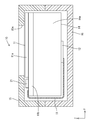
- FIG. 1 is a schematic plan view showing a connection configuration of a liquid crystal panel, a flexible substrate, and a control circuit board on which a driver according to Embodiment 1 of the present invention is mounted.
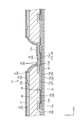
- Schematic sectional view showing the sectional structure of the liquid crystal panel A plan view schematically showing a wiring configuration of an array substrate constituting a liquid crystal panel
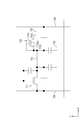
- Circuit diagram showing circuit configuration of pixel in display section of array substrate
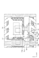
- FIG. 6 is an enlarged plan view in the vicinity of the pixel TFT and the resistive TFT.
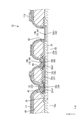
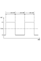
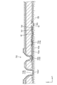
- Sectional view taken along line ix-ix in FIG. The figure showing the change for every frame regarding the voltage value of the data signal supplied to the pixel source electrode part of the pixel TFT
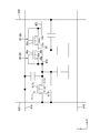
- the circuit diagram which shows the circuit structure of the pixel in the display part of the array substrate which concerns on Embodiment 2 of this invention.
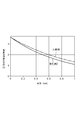
- a graph showing the change over time of the voltage related to the pixel electrode charged by the pixel TFT The circuit diagram which shows the circuit structure of the pixel in the display part of the array substrate which concerns on Embodiment 3 of this invention.
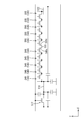
- the circuit diagram which shows the circuit structure of the pixel in the display part of the array substrate which concerns on Embodiment 4 of this invention.
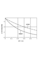
- a graph showing the change over time of the voltage related to the pixel electrode charged by the pixel TFT The circuit diagram which shows the circuit structure of the pixel in the display part of the array substrate which concerns on Embodiment 5 of this invention.
- the circuit diagram which shows the circuit structure of the pixel in the display part of the array substrate which concerns on Embodiment 6 of this invention.
- a graph showing the change over time of the voltage related to the pixel electrode charged by the pixel TFT The circuit diagram which shows the circuit structure of the pixel in the display part of the array substrate which concerns on Embodiment 7 of this invention.
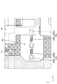
- An enlarged plan view of the vicinity of the pixel TFT and the resistive wiring part in the display part of the array substrate Xxv-xxv sectional view of FIG. A graph showing the change over time of the voltage related to the pixel electrode charged by the pixel TFT
- the circuit diagram which shows the circuit structure of the pixel in the display part of the array substrate which concerns on Embodiment 8 of this invention.
- FIG. 9 An enlarged plan view of the vicinity of the pixel TFT and the resistive TFT in the display section of the array substrate Xxix-xxix line cross-sectional view of FIG.
- the circuit diagram which shows the circuit structure of the pixel in the display part of the array substrate which concerns on Embodiment 9 of this invention.
- the top view which expanded the TFT for pixels and resistive wiring part vicinity in the display part of the array substrate which concerns on Embodiment 10 of this invention.
- the circuit diagram which shows the circuit structure of the pixel in the display part of the array substrate which concerns on Embodiment 11 of this invention.
- circuit diagram which shows the circuit structure of the pixel in the display part of the array substrate which concerns on Embodiment 12 of this invention.
- circuit diagram which shows the circuit structure of the pixel in the display part of the array substrate which concerns on Embodiment 13 of this invention.
- FIGS. 1 A first embodiment of the present invention will be described with reference to FIGS.
- the liquid crystal display device 10 is illustrated.
- a part of each drawing shows an X axis, a Y axis, and a Z axis, and each axis direction is drawn to be a direction shown in each drawing.
- FIG. 2 and the like are used as a reference, and the upper side of the figure is the front side and the lower side of the figure is the back side.
- the liquid crystal display device 10 drives a liquid crystal panel (display device) 11 having a display unit AA capable of displaying an image and a non-display unit NAA outside the display unit AA, and the liquid crystal panel 11.
- a backlight device (illumination device) 14 which is an external light source for supplying light to the liquid crystal panel 11.
- the liquid crystal display device 10 also includes a pair of front and back exterior members 15 and 16 for housing and holding the liquid crystal panel 11 and the backlight device 14 assembled to each other.
- the liquid crystal display device 10 includes a notebook computer (including a tablet notebook computer), a mobile phone (including a smartphone), a portable information terminal (including an electronic book, a PDA, etc.), a digital photo frame, It is used for various electronic devices (not shown) such as portable game machines and electronic ink paper. For this reason, the screen size of the liquid crystal panel 11 constituting the liquid crystal display device 10 is set to about several inches to several tens of inches, and is generally classified into a small size and a small size.
- the backlight device 14 includes a chassis 14a having a substantially box shape that opens toward the front side (the liquid crystal panel 11 side), and a light source (not shown) disposed in the chassis 14a (for example, a cold cathode tube, LED, organic EL, etc.) and an optical member (not shown) arranged to cover the opening of the chassis 14a.
- the optical member has a function of converting light emitted from the light source into a planar shape.
- the liquid crystal panel 11 has a vertically long rectangular shape (rectangular shape) as a whole, and is displayed at a position offset toward one end side (the upper side shown in FIG. 1) in the long side direction.
- a portion (active area) AA is arranged, and a driver 21 and a flexible substrate 13 are respectively attached at positions offset toward the other end side (the lower side shown in FIG. 1) in the long side direction.
- an area outside the display area AA is a non-display area (non-active area) NAA in which no image is displayed.
- the non-display area NAA is a substantially frame-shaped area (CF described later) surrounding the display area AA.
- the area secured on the other end side in the long side direction includes the mounting area (mounting area) for the driver 21 and the flexible substrate 13.
- the short side direction in the liquid crystal panel 11 coincides with the X-axis direction of each drawing, and the long side direction coincides with the Y-axis direction of each drawing.
- a one-dot chain line having a frame shape slightly smaller than the CF substrate 11a represents the outer shape of the display portion AA, and a region outside the solid line is a non-display portion NAA.
- the control circuit board 12 is attached to the back surface of the chassis 14a (the outer surface opposite to the liquid crystal panel 11 side) of the backlight device 14 with screws or the like.
- the control circuit board 12 is mounted with electronic components for supplying various input signals to the driver 21 on a board made of paper phenol or glass epoxy resin, and wiring (conductive path) of a predetermined pattern (not shown) is provided. Routed formation.
- One end (one end side) of the flexible substrate 13 is electrically and mechanically connected to the control circuit board 12 via an ACF (Anisotropic Conductive Film) (not shown).
- the flexible substrate (FPC substrate) 13 includes a base material made of a synthetic resin material (for example, polyimide resin) having insulating properties and flexibility, and a large number of wirings are provided on the base material. It has a pattern (not shown), and one end in the length direction is connected to the control circuit board 12 arranged on the back side of the chassis 14a as described above, while the other end Since the portion (the other end side) is connected to the array substrate 11 b in the liquid crystal panel 11, the liquid crystal display device 10 is bent in a folded shape so that the cross-sectional shape is substantially U-shaped.
- a synthetic resin material for example, polyimide resin
- the wiring pattern is exposed to the outside to form terminal portions (not shown), and these terminal portions are respectively connected to the control circuit board 12 and the liquid crystal panel 11. Are electrically connected to each other. Thereby, an input signal supplied from the control circuit board 12 side can be transmitted to the liquid crystal panel 11 side.
- the driver 21 is composed of an LSI chip having a drive circuit therein, and operates based on a signal supplied from a control circuit board 12 that is a signal supply source. An input signal supplied from the control circuit board 12 is processed to generate an output signal, and the output signal is output to the display unit AA of the liquid crystal panel 11.
- the driver 21 has a horizontally long rectangular shape when viewed in a plan view (having a long shape along the short side of the liquid crystal panel 11), and with respect to the non-display portion NAA of the liquid crystal panel 11 (an array substrate 11b described later). It is mounted directly, that is, COG (Chip On Glass).
- the long side direction of the driver 21 coincides with the X-axis direction (the short side direction of the liquid crystal panel 11), and the short side direction coincides with the Y-axis direction (the long side direction of the liquid crystal panel 11).
- the liquid crystal panel 11 includes a pair of substrates 11 a and 11 b and a liquid crystal layer including liquid crystal molecules that are interposed between the substrates 11 a and 11 b and that are substances whose optical characteristics change with application of an electric field ( Liquid crystal) 11c, and both substrates 11a and 11b are bonded together with a sealant (not shown) while maintaining a gap corresponding to the thickness of the liquid crystal layer 11c.
- the liquid crystal panel 11 according to the present embodiment is an FFS (Fringe Field Switching) mode in which the operation mode is further improved from an IPS (In-Plane Field Switching) mode.
- the pixel electrode unit (pixel unit) 18 and the common electrode unit (counter electrode unit, common electrode unit) 22 are formed together, and the pixel electrode unit 18 and the common electrode unit 22 are arranged in different layers. is there.
- the front side (front side) is a CF substrate (counter substrate) 11a
- the back side (back side) is an array substrate (display element) 11b.
- Each of the CF substrate 11a and the array substrate 11b includes a glass substrate GS that is substantially transparent (having high translucency), and is formed by laminating various films on the glass substrate GS.
- the CF substrate 11a has a short side dimension substantially equal to that of the array substrate 11b as shown in FIGS.
- the long side dimension is smaller than that of the array substrate 11b. It is bonded to 11b with one end (upper side shown in FIG. 1) in the long side direction aligned. Therefore, the other end (the lower side shown in FIG. 1) of the array substrate 11b in the long side direction is in a state in which the CF substrate 11a does not overlap over a predetermined range and both the front and back plate surfaces are exposed to the outside. Here, a mounting area for the driver 21 and the flexible board 13 is secured. Alignment films 11d and 11e for aligning liquid crystal molecules contained in the liquid crystal layer 11c are formed on the inner surfaces of both the substrates 11a and 11b, respectively.
- the alignment films 11d and 11e are made of, for example, polyimide, and are formed in a solid shape over almost the entire area along the plate surfaces of both the substrates 11a and 11b.
- the alignment films 11d and 11e are photo-alignment films capable of aligning liquid crystal molecules along the irradiation direction of light in a specific wavelength region (for example, ultraviolet rays).
- polarizing plates 11f and 11g are attached to the outer surface sides of both the substrates 11a and 11b, respectively.
- the array substrate 11b includes a first metal film (first conductive film, gate metal film) 34, a gate insulating film (insulating film, first film) in order from the lower layer (glass substrate GS) side.
- the first metal film 34, the semiconductor film 36, and the second metal film 38 are shown in a shaded manner.
- the first metal film 34 is formed of a laminated film of titanium (Ti) and copper (Cu).
- the gate insulating film 35 is laminated at least on the upper layer side of the first metal film 34, and is made of, for example, silicon oxide (SiO2).
- the semiconductor film 36 is made of a thin film using an oxide semiconductor as a material. Specific oxide semiconductors include, for example, indium (In), gallium (Ga), zinc (Zn), oxygen (O In—Ga—Zn—O-based semiconductors (indium gallium zinc oxide) are used.
- the oxide semiconductor (In—Ga—Zn—O-based semiconductor) forming the semiconductor film 36 may be amorphous, but preferably has crystallinity including a crystalline portion.
- crystalline oxide semiconductor for example, a crystalline In—Ga—Zn—O-based semiconductor in which the c-axis is aligned substantially perpendicular to the layer surface is preferable.
- the crystal structure of such an oxide semiconductor is disclosed in, for example, Japanese Patent Application Laid-Open No. 2012-134475.
- Japanese Patent Application Laid-Open No. 2012-134475 the entire disclosure of Japanese Patent Application Laid-Open No. 2012-134475 is incorporated herein by reference.
- the protective film 37 is made of silicon oxide (SiO 2).
- the second metal film 38 is formed of a laminated film of titanium (Ti) and copper (Cu).
- the first interlayer insulating film 39 is made of silicon oxide (SiO 2).
- the organic insulating film 40 is made of an acrylic resin material (for example, polymethyl methacrylate resin (PMMA)), which is an organic material, and functions as a planarizing film.
- Both the first transparent electrode film 23 and the second transparent electrode film 24 are made of a transparent electrode material such as ITO (Indium Tin Oxide) or ZnO (Zinc Oxide).
- the second interlayer insulating film 41 is made of silicon nitride (SiNx).
- the first transparent electrode film 23 and the second transparent electrode film 24 are formed only on the display portion AA of the array substrate 11b and not on the non-display portion NAA.
- a solid pattern (partially over the entire surface of the array substrate 11b). Have an opening).
- the first metal film 34, the semiconductor film 36, and the second metal film 38 are formed with a predetermined pattern on both the display area AA and the non-display area NAA of the array substrate 11b.
- the display unit AA of the array substrate 11b is provided with a large number of pixel TFTs (pixel transistors) 17 and pixel electrode units 18 which are switching elements arranged in a matrix.
- the gate wiring (scanning signal line, row control line) 19 and the source wiring (data signal line, column control line) 20 having a lattice shape surround the pixel TFT 17 and the pixel electrode portion 18. It is arranged.
- the pixel TFTs 17 and the pixel electrode portions 18 are arranged in parallel in a matrix at the intersection of the gate wiring 19 and the source wiring 20 that form a lattice.
- the gate wiring 19 is made of the first metal film 34
- the source wiring 20 is made of the second metal film 38
- the gate insulating film 35 and the protective film 37 are interposed between the intersecting portions.
- the gate wiring 19 and the source wiring 20 are respectively connected to the pixel gate electrode portion 17a and the pixel source electrode portion 17b of the pixel TFT 17, and the pixel electrode portion 18 is a pixel of the pixel TFT 17. It is connected to the drain electrode portion 17c for use (FIG. 8).
- the gate wiring 19 is arranged so as to overlap with one end (lower side shown in FIG. 6) of the pixel electrode portion 18 in a plan view (viewed from the normal direction to the plate surface of the array substrate 11b). . Therefore, a capacitance Cgd is formed between the gate wiring 19 and the pixel electrode portion 18 (see FIG. 5). Further, a capacitance Csd1 is formed between the source wiring 20 and the pixel electrode portion 18 connected to the pixel TFT 17 to which the source wiring 20 is connected (see FIG. 5). In addition, between the source electrode 20 connected to the pixel TFT 17 connected to the pixel electrode unit 18 and the source electrode 20 adjacent to the pixel electrode unit 18 between the pixel electrode unit 18 and the pixel electrode unit 18. Has a capacitance Csd2 (see FIG. 5).
- the array substrate 11b has an auxiliary capacitance wiring portion (storage capacitance wiring portion, Cs) that is parallel to the gate wiring 19 and overlaps a part of the pixel electrode portion 18 in a plan view.
- Wiring section) 25 is provided.
- the auxiliary capacitance wiring portion 25 is made of the same first metal film 34 as the gate wiring 19 and is arranged so as to overlap with the other end (upper side shown in FIG. 6) of the pixel electrode portion 18 in a plan view, that is, the Y axis.
- the gate electrode 19 is disposed on the opposite side with the central portion of the pixel electrode portion 18 interposed therebetween.
- the auxiliary capacitance wiring part 25 is connected between the pixel electrode part 18 on which it is superimposed and the gate wiring 19 connected to the pixel electrode part 18 adjacent to the upper side shown in FIG. , Adjacent to each other with a predetermined interval in the Y-axis direction.
- the auxiliary capacitance wiring section 25 is arranged alternately with the gate wiring 19 in the Y-axis direction.
- a predetermined reference potential is applied to the auxiliary capacitance wiring portion 25.
- a capacitance Ccs is formed between the auxiliary capacitance wiring portion 25 and the pixel electrode portion 18 (see FIG. 5). In FIG. 5, illustration of the auxiliary capacitance wiring portion 25 is omitted.
- the pixel TFT 17 is arranged on the gate wiring 19, that is, the whole of the pixel TFT 17 overlaps with the gate wiring 19 in a plan view, and a part of the gate wiring 19 is used for the pixel.
- the pixel gate electrode portion 17a of the TFT 17 is configured, and the portion of the source wiring 20 that overlaps the gate wiring 19 when viewed in plan forms the pixel source electrode portion 17b of the pixel TFT 17.
- the pixel TFT 17 has a pixel drain electrode portion 17c that is in an island shape by being arranged opposite to the pixel source electrode portion 17b with a predetermined interval in the X-axis direction.
- the pixel drain electrode portion 17c is formed of the same second metal film 38 as the pixel source electrode portion 17b (source wiring 20), and is planar with one end of the pixel electrode portion 18 (a non-formation portion of a slit 18a described later). It is set as the arrangement
- the pixel drain electrode portion 17c is connected to a drain wiring 29 made of the same second metal film 38.
- the drain wiring 29 extends from the connected pixel drain electrode portion 17c along the Y-axis direction. 7 extends toward the lower side, that is, toward the auxiliary capacitance wiring portion 25 side, and extends to the auxiliary capacitance wiring portion 25 and the adjacent pixel electrode portion 18 (specifically, the pixel drain electrode portion 17c).
- a capacitance forming portion 29a for forming a capacitance Ccs is formed by overlapping the pixel electrode portion 18 connected to the pixel electrode portion 18 on the lower side shown in FIG. ing.
- the portion of the gate wiring 19 that is not overlapped with the source wiring 20 in plan view is formed so that the line width is wider than the portion that overlaps with the source wiring 20 in plan view.
- the portion of the source wiring 20 that overlaps the gate wiring 19 and the auxiliary capacitance wiring portion 25 in plan view is compared with the portion that does not overlap the gate wiring 19 and the auxiliary capacitance wiring portion 25 in plan view. The line width is increased.
- the pixel TFT 17 includes a pixel gate electrode portion 17a made of the first metal film 34 and a pixel channel portion 17d made of the semiconductor film 36 and overlapping the pixel gate electrode portion 17a in plan view. And a protective portion 17e formed by penetrating two opening portions 17e1 and 17e2 at positions overlapping with the pixel channel portion 17d in plan view, and a second metal film 38.
- the pixel source electrode portion 17b connected to the pixel channel portion 17d through one of the openings 17e1 and 17e2 and the other of the two openings 17e1 and 17e2 formed of the second metal film 38.
- a pixel drain electrode portion 17c connected to the pixel channel portion 17d through the opening 17e2.
- the pixel gate electrode portion 17a includes a portion of the gate wiring 19 that overlaps at least the pixel source electrode portion 17b, the pixel drain electrode portion 17c, and the pixel channel portion 17d in plan view.
- the pixel channel portion 17d extends along the X-axis direction and bridges the pixel source electrode portion 17b and the pixel drain electrode portion 17c so that electrons can move between the electrode portions 17b and 17c.
- the semiconductor film 36 forming the pixel channel portion 17d is, for example, an In—Ga—Zn—O-based (mainly composed of indium (In), gallium (Ga), zinc (Zn), oxygen (O)).
- An oxide semiconductor thin film made of an oxide) semiconductor indium gallium zinc oxide), etc.
- the oxide semiconductor thin film has an electron mobility of, for example, about 20 to 50 times higher than that of an amorphous silicon thin film. Therefore, the pixel TFT 17 can be easily miniaturized to maximize the amount of light transmitted through the pixel electrode portion 18, which is suitable for achieving high definition and low power consumption.
- the off characteristics of the pixel TFT 17 are higher than when the amorphous silicon is used as the material for the pixel channel portion. Since it is extremely low, about 1 / min, the voltage holding ratio of the pixel electrode portion 18 becomes high, which is useful for reducing power consumption.
- the pixel gate electrode portion 17a is disposed in the lowermost layer, and the pixel channel portion 17d is stacked on the upper layer side with the gate insulating film 35 interposed therebetween. It is a staggered type and has a laminated structure similar to a pixel TFT having a general amorphous silicon thin film.
- the pixel electrode portion 18 is made of the second transparent electrode film 24, and has a vertically long substantially rectangular shape when viewed as a whole in a region surrounded by the gate wiring 19 and the source wiring 20. (Substantially rectangular shape).
- One end portion of the pixel electrode portion 18 overlaps with the gate wiring 19 in a plan view, whereas the portion other than the overlapping portion is not overlapped with the gate wiring 19 in a plan view.
- the non-overlapping portion is formed in a substantially comb-like shape by providing a plurality of long slits 18a (two in FIG. 7).
- the slit 18a extends to a part of the pixel electrode portion 18 that is overlapped with the gate wiring 19 in a plan view.
- the lower end position of the pixel electrode portion 18 shown in FIG. 7 is between the lower end position of the gate wiring 19 and the lower end position of the pixel drain electrode portion 17c.
- the arrangement is closer to the lower end position.
- the pixel electrode portion 18 is formed on the second interlayer insulating film 41, and the second interlayer insulating film 41 is interposed between the pixel electrode portion 18 and the common electrode portion 22 described below.
- the first interlayer insulating film 39, the organic insulating film 40, and the second interlayer insulating film 41 disposed on the lower layer side of the pixel electrode unit 18, the pixel drain electrode unit 17c and the pixel electrode unit 18 are overlapped in a plan view.
- a pixel contact hole (contact hole) 26 is formed so as to penetrate vertically, and the pixel electrode portion 18 is connected to the pixel drain electrode portion 17 c through the pixel contact hole 26.
- a current flows between the pixel source electrode portion 17b and the pixel drain electrode portion 17c via the pixel channel portion 17d, and the pixel electrode portion. Charges are stored in 18 and charged to a predetermined potential.
- the pixel contact hole 26 is formed so as to penetrate through the first interlayer insulating film 39 and the organic insulating film 40, and through the second interlayer insulating film 41.
- the upper contact hole 31 overlaps when viewed in plan view, and will be described in detail later. However, the planar shapes of the contact holes 30 and 31 are different from each other.
- a portion of the pixel electrode portion 18 disposed in the lower layer side contact hole 30 and the upper layer side contact hole 31 is a pixel electrode side connection portion connected to the pixel drain electrode portion 17c.
- the portion of the pixel drain electrode portion 17 c that faces the front side through the lower layer side contact hole 30 and the upper layer side contact hole 31 is connected to the pixel electrode side connection portion of the pixel electrode portion 18. It is said.
- the common electrode portion 22 is formed of a first transparent electrode film 23, and has a so-called solid pattern covering almost the entire surface of the display portion AA of the array substrate 11b.
- the common electrode portion 22 is disposed so as to be sandwiched between the organic insulating film 40 and the second interlayer insulating film 41.
- the common electrode portion 22 is opposed to the pixel electrode portion 18 via the second interlayer insulating film 41, and a capacitance Clc is formed therebetween. Since the reference potential (common potential) Vcom is applied to the common electrode portion 22 from a common wiring (not shown), the potential applied to the pixel electrode portion 18 by the pixel TFT 17 as described above is controlled. A predetermined potential difference can be generated between 18 and 22.
- the liquid crystal layer 11c When a potential difference is generated between the electrode portions 18 and 22, the liquid crystal layer 11c has a normal direction with respect to the plate surface of the array substrate 11b in addition to the component along the plate surface of the array substrate 11b by the slit 18a of the pixel electrode portion 18. Since a fringe electric field (diagonal electric field) containing the above component is applied, among the liquid crystal molecules contained in the liquid crystal layer 11c, those present on the pixel electrode portion 18 in addition to those present in the slit 18a Can be switched appropriately. Accordingly, the aperture ratio of the liquid crystal panel 11 is increased, and a sufficient amount of transmitted light can be obtained, and high viewing angle performance can be obtained.
- an opening 22a is formed in a portion overlapping with a part of the pixel TFT 17 in plan view (see FIG. 8).
- the reference potential of the auxiliary capacitance wiring portion 25 is set to the same potential as the reference potential Vcom of the common electrode portion 22.
- An alignment film 11d is provided on the surfaces of the color filter 11h and the light shielding layer 11i.
- one display which is a display unit, is formed by a set of three colored portions of R (red), G (green), and B (blue) and three pixel electrode portions 18 facing the colored portions. Pixels are configured.
- the display pixel includes a red pixel having an R colored portion, a green pixel having a G colored portion, and a blue pixel having a B colored portion.
- the pixels of each color constitute a pixel group by being repeatedly arranged along the row direction (X-axis direction) on the plate surface of the liquid crystal panel 11, and this pixel group constitutes the column direction (Y-axis direction). Many are arranged side by side.
- a column control circuit portion 27 is provided at a position adjacent to the short side portion of the display portion AA, as shown in FIG.
- a row control circuit section 28 is provided at a position adjacent to the long side section.
- the column control circuit unit 27 and the row control circuit unit 28 can perform control for supplying an output signal from the driver 21 to the pixel TFT 17.
- the column control circuit unit 27 and the row control circuit unit 28 are monolithically formed on the array substrate 11 b based on the semiconductor film 36 made of the same oxide semiconductor as the pixel TFT 17, and thereby output signals to the pixel TFT 17.
- the column control circuit unit 27 and the row control circuit unit 28 are simultaneously patterned on the array substrate 11b by a known photolithography method when patterning the pixel TFTs 17 and the like in the manufacturing process of the array substrate 11b.
- the column control circuit unit 27 is located between the display unit AA and the driver 21 in the position adjacent to the lower short side portion shown in FIG. It is arranged in an intermediate position, and is formed in a horizontally long rectangular range extending along the X-axis direction (the arrangement direction of the source wirings 20).
- the column control circuit unit 27 is connected to the source line 20 arranged in the display unit AA, and also switches a data signal included in the output signal from the driver 21 to each source line 20 (RGB switch circuit). have.
- the column control circuit unit 27 distributes the data signal from the driver 21 to the R, G, and B source wirings 20 and supplies the data signals to the R, G, and B source by the switch circuit. ing.
- the column control circuit unit 27 can include an attached circuit such as a level shifter circuit or an ESD protection circuit.
- the row control circuit unit 28 is arranged at a position adjacent to the long side portion on the left side shown in FIG. 4 in the display unit AA. It is formed in a vertically long range extending along (direction).
- the row control circuit unit 28 is connected to the gate wiring 19 arranged in the display unit AA, and supplies a scanning signal included in the output signal from the driver 21 to each gate wiring 19 at a predetermined timing to each gate.
- a scanning circuit that sequentially scans the wiring 19 is provided. Specifically, a large number of gate wirings 19 are arranged in parallel along the Y-axis direction in the display unit AA of the array substrate 11b, whereas the row control circuit unit 28 is connected from the driver 21 by the scanning circuit.
- the scanning circuit included in the row control circuit unit 28 includes a buffer circuit for amplifying the scanning signal.
- the row control circuit unit 28 can include an attached circuit such as a level shifter circuit or an ESD protection circuit.
- the column control circuit unit 27 and the row control circuit unit 28 are connected to the driver 21 by connection wiring formed on the array substrate 11b.
- the pixel TFT 17 when manufacturing the array substrate 11b constituting the liquid crystal panel 11 having the above-described configuration, charges are accumulated in the pixel electrode portion 18 in the manufacturing process, or in the inspection process performed between the manufacturing processes, the pixel TFT 17. In some cases, the charge is accumulated in the pixel electrode portion 18 as the test is activated. Even in such a case, since the pixel TFT 17 uses an oxide semiconductor as the semiconductor film 36 forming the pixel channel portion 17d, the pixel TFT 17 has high off characteristics. For this reason, as described above, charges accumulated in the pixel electrode portion 18 in the manufacturing process and the inspection process tend to remain for a long period of time.
- a resistive TFT (transistor) 32 is formed as a resistive element.
- the resistive TFT 32 has at least a gate electrode portion 32a, a source electrode portion 32b, a drain electrode portion 32c, and a channel portion 32d that connects the source electrode portion 32b and the drain electrode portion 32c.
- the gate electrode portion 32 a and the source electrode portion 32 b are connected to the pixel electrode portion 18, and the drain electrode portion 32 c is connected to the common electrode portion 22.
- the drain electrode portion 32c is set to the same potential as the common electrode portion 22, whereas the gate electrode portion 32a and the source electrode portion 32b are both set to the same potential as the pixel electrode portion 18. It can be said that it functions substantially as a diode and is a “diode-type transistor”. As shown in FIG. 6, the resistive TFT 32 has a position adjacent to the pixel TFT 17 in a plan view, specifically, a gate wiring 19 connected to the pixel TFT 17 and a source wiring 20 connected to the pixel TFT 17.
- the gate electrode portion 32a overlaps the entire area of the source electrode portion 32b, the drain electrode portion 32c, and the channel portion 32d in a plan view, and the drain electrode portion 32c side with respect to the source electrode portion 32b is It is formed in a form having a gate extension part 32a1 extending to the opposite side.
- the pixel electrode portion 18 includes a pixel extension portion 18b that overlaps a part of the resistive TFT 32, specifically, the drain electrode portion 32c and the gate extension portion 32a1 of the gate electrode portion 32a in a plan view. Is formed.
- the resistive TFT 32 includes a gate electrode part 32a made of the first metal film 34 and a channel part 32d made of the semiconductor film 36 and overlapping the gate electrode part 32a in plan view. And a protective part 32e formed by penetrating two openings 32e1 and 32e2 at a position that is formed of the protective film 37 and overlaps the channel part 32d in plan view, and two openings formed of the second metal film 38.
- the source electrode part 32b connected to the channel part 32d through one opening part 32e1 of 32e1 and 32e2, and the channel part through the other opening part 32e2 of the two opening parts 32e1 and 32e2 made of the second metal film 38.
- a drain electrode portion 32c connected to 32d.
- the gate electrode portion 32 a is arranged in a form separated (independent) from the gate wiring 19 and the auxiliary capacitance wiring portion 25.
- the channel part 32d extends along the X-axis direction and bridges the source electrode part 32b and the drain electrode part 32c, thereby allowing electrons to move between the electrode parts 32b and 32c.
- the semiconductor film 36 constituting the channel portion 32d is made of the same oxide semiconductor (In—Ga—Zn—O-based semiconductor) as the pixel channel portion 17d constituting the pixel TFT 17.
- a distance along the X-axis direction between the source electrode portion 32b and the drain electrode portion 32c is a channel length (length dimension), and the direction from the source electrode portion 32b toward the drain electrode portion 32c (X-axis direction)
- the dimension along the Y-axis direction orthogonal to the channel width is defined as the channel width (width dimension)
- the ratio (L / W) obtained by dividing the channel length by the channel width is the pixel channel constituting the pixel TFT 17. It is formed to be larger than the ratio obtained by dividing the same channel length in the portion 17d by the channel width.
- the resistance value relating to the charges moving between the source electrode portion 32b and the drain electrode portion 32c through the channel portion 32d is changed between the pixel source electrode portion 17b and the pixel use through the pixel channel portion 17d constituting the pixel TFT 17.
- the resistance value is relatively larger than the resistance value related to the charge moving between the drain electrode portion 17c. Note that the channel length and the channel width of the channel portion 32d are smaller than the channel length and the channel width in the pixel channel portion 17d, respectively.
- a gate contact hole 42 is formed so as to penetrate vertically in a position overlapping in plan view. Through this gate contact hole 42, the pixel extension 18 b is a gate electrode portion. 32a.
- the pixel extending portion 18b and the drain electrode portion 32c are viewed in plan.
- a drain contact hole 43 is formed so as to penetrate vertically, and the pixel extension portion 18 b is connected to the drain electrode portion 32 c through the drain contact hole 43.
- An opening is formed in the common electrode portion 22 so as to surround the gate contact hole 42 and the drain contact hole 43.
- the position overlapping with the common electrode part 22 and the source electrode part 32b in a plan view is used for the source.
- a contact hole 44 is formed so as to penetrate vertically, and the common electrode portion 22 is connected to the source electrode portion 32 b through the source contact hole 44.
- the gate electrode portion of the resistive TFT 32 that has the same potential as the pixel electrode portion 18.
- a potential difference is generated between the drain electrode portion 32c having the same potential as the common electrode portion 22 and the source electrode portion 32b. Therefore, the resistive TFT 32 substantially functions as a diode, and a current flows (a charge is moved) between the source electrode portion 32b and the drain electrode portion 32c via the channel portion 32d.
- electric charges move between the pixel electrode unit 18 and the common electrode unit 22, and eventually the pixel electrode unit 18 and the common electrode unit 22 have the same potential. This makes it difficult for image sticking or flicker to occur in the display image without performing special control.
- the driving method of the pixel TFT 17 will be described in detail.
- the pixel TFT 17 is turned on by a scanning signal supplied to the pixel gate electrode portion 17a through the gate wiring 19 at a predetermined timing, the source wiring 20 is connected.
- the data signal supplied to the pixel source electrode portion 17b is transmitted to the pixel drain electrode portion 17c via the pixel channel portion 17d.
- the reference potential Vcom supplied to the common electrode unit 22 is always a constant value.
- the pixel TFT 17 is driven by so-called “frame inversion driving” in which the polarity is inverted every frame display period, and is relative to the reference potential Vcom of the common electrode portion 22.
- the high potential + V and the potential ⁇ V relatively lower than the reference potential Vcom of the common electrode portion 22 are alternately supplied to the pixel electrode portion 18 via the pixel TFT 17 every frame display period. It has become.
- the frame rate is set to 60 fps, for example.
- the resistive TFT 32 is reverse-biased. It is assumed that only a charge of about the leakage current flows between the electrode part 32b and the drain electrode part 32c. In any case, since the amount of movement per unit time in the charge moving between the pixel electrode portion 18 and the common electrode portion 22 via the resistive TFT 32 is very small, it resists the charge.
- the characteristic TFT 32 constitutes a large resistance component.
- a sufficient time can be taken until the potential of the pixel electrode portion 18 reaches the reference potential Vcom of the common electrode portion 22, and the potential of the pixel electrode portion 18 instantaneously reaches the reference potential Vcom of the common electrode portion 22.
- This makes it suitable for maintaining the potential of the pixel electrode portion 18 charged by the pixel TFT 17 when displaying an image on the liquid crystal panel 11 for a certain period (for example, one frame display period) during normal use. A situation in which the display quality of the image is impaired is less likely to occur.
- the pixel TFT 18 is not limited to the case where the pixel electrode 18 is charged.
- the liquid crystal panel (display device) 11 of this embodiment includes a pixel electrode unit (pixel unit) 18 and a pixel TFT that is connected to the pixel electrode unit 18 and can charge the pixel electrode unit 18.
- (Switching element) 17 a common electrode portion (reference potential portion) 22 that is set as a reference potential, and a pixel electrode portion 18 and a common electrode portion 22 that are connected to each other between the pixel electrode portion 18 and the common electrode portion 22.
- a resistive TFT 32 which is a resistive element that constitutes a resistance component against charges moving between the common electrode portions 22.
- the potential of the pixel electrode unit 18 is, for example, that of the common electrode unit 22.
- the potential is higher than the reference potential, the charge moves from the pixel electrode unit 18 to the common electrode unit 22 through the resistive TFT 32 that is a resistive element, and conversely, the potential of the pixel electrode unit 18 is the common electrode.
- the potential is lower than the reference potential of the portion 22, the charge is transferred from the common electrode portion 22 to the pixel electrode portion 18 via the resistive TFT 32, which is a resistive element.
- the resistive TFT 32 which is a resistive element, constitutes a resistance component for charges moving between the pixel electrode portion 18 and the common electrode portion 22, so that the potential of the pixel electrode portion 18 reaches the reference potential.
- the time until the potential of the pixel electrode section 18 instantaneously reaches the reference potential can be avoided.
- the resistive element includes at least a gate electrode portion 32a, a source electrode portion 32b, a drain electrode portion 32c, and a channel portion 32d that connects the source electrode portion 32b and the drain electrode portion 32c.
- the gate electrode portion 32a is connected to either the pixel electrode portion 18 or the common electrode portion 22, and one of the source electrode portion 32b and the drain electrode portion 32c is connected to the pixel electrode portion 18 and the other is connected to the other.
- Resistive TFTs (transistors) 32 connected to the common electrode portion 22 are included. In this way, the gate electrode portion 32a is set to the same potential as either the pixel electrode portion 18 or the common electrode portion 22, and one of the source electrode portion 32b and the drain electrode portion 32c is the pixel electrode.
- the resistive TFT 32 substantially functions as a diode, and charges are transferred between the source electrode part 32b and the drain electrode part 32c via the channel part 32d.
- the resistive TFT 32 is forward-biased or reverse-biased according to the potential charged in the pixel electrode unit 18 by the pixel TFT 17.
- the threshold voltage of the resistive TFT 32 is exceeded.
- reverse bias only the charge about the leakage current of the resistive TFT 32 flows, and the amount of charge transfer is extremely small.
- the resistive TFT 32 constitutes a resistance component with respect to the charge moving between the pixel electrode portion 18 and the common electrode portion 22, the potential until the potential of the pixel electrode portion 18 becomes the reference potential. You can earn enough time. As a result, when an image is displayed on the liquid crystal panel 11, a situation in which the display quality related to the display image is impaired is less likely to occur.
- the switching elements include a pixel gate electrode portion 17a, a pixel source electrode portion 17b, a pixel drain electrode portion 17c connected to the pixel electrode portion 18, a pixel source electrode portion 17b, and a pixel drain electrode portion.
- the pixel TFT 17 includes at least a pixel channel portion 17d that connects to the pixel channel portion 17d.
- the resistive TFT 32 that constitutes the resistive element includes the pixel TFT 17 that the channel portion 32d constitutes the switching element. It is made of the same material as the pixel channel portion 17d. In this case, the material is shared between the pixel channel portion 17d of the pixel TFT 17 constituting the switching element and the channel portion 32d of the resistive TFT 32 constituting the resistive element, thereby reducing the manufacturing cost. It will be useful to plan.
- the length dimension (channel length), which is the distance between the source electrode section 32b and the drain electrode section 32c in the channel section 32d, is divided by the width dimension (channel width).
- the ratio is larger than the ratio obtained by dividing the length dimension, which is the distance between the pixel source electrode part 17b and the pixel drain electrode part 17c in the pixel channel part 17d of the pixel TFT 17 constituting the switching element, by the width dimension. It is formed to be large.
- the resistance value related to the charge moving between the source electrode part 32b and the drain electrode part 32c via the channel part 32d is the pixel constituting the switching element.
- the resistance value is larger than the resistance value related to the charge moving between the pixel source electrode portion 17 b and the pixel drain electrode portion 17 c via the pixel channel portion 17 d.
- the time until the potential of the pixel electrode portion 18 is set to the reference potential can be sufficiently obtained by the resistive TFT 32 constituting the resistive element, so that when the image is displayed on the liquid crystal panel 11, the display image is displayed. Such a display quality is more unlikely to occur.
- the gate electrode portion 32 a and the source electrode portion 32 b are connected to the pixel electrode portion 18, and the drain electrode portion 32 c is connected to the common electrode portion 22.
- the resistive TFT 32 constituting the resistive element is forward biased. Charges move from the source electrode part 32b (pixel electrode part 18) having the same potential as 32a to the drain electrode part 32c (common electrode part 22).
- the resistive TFT 32 constituting the resistive element is reverse-biased, so that the drain electrode portion 32c (common electrode) The charge moves from the portion 22) to the source electrode portion 32b (pixel electrode portion 18) having the same potential as the gate electrode portion 32a.
- the resistive TFT 32 constitutes a resistance component with respect to the charge moving between the pixel electrode portion 18 and the common electrode portion 22, the potential until the potential of the pixel electrode portion 18 becomes the reference potential. You can earn enough time. As a result, when an image is displayed on the liquid crystal panel 11, a situation in which the display quality related to the display image is impaired is less likely to occur.
- a common electrode portion 22 that forms a capacitance with the pixel electrode portion 18 is provided, and the reference potential portion is composed of the common electrode portion 22.
- the reference potential portion where the charge is transferred to and from the pixel electrode portion 18 by the resistive TFT 32 that is a resistive element is used as the common electrode portion that forms a capacitance between the pixel electrode portion 18 and the reference potential portion. Therefore, the potential difference between the pixel electrode portion 18 and the common electrode portion 22 can be brought close to 0 with the movement of charges through the resistive TFT 32 that is a resistive element. Thereby, image sticking, flicker, etc. can be made harder to occur in the display image.
- the switching elements include a pixel gate electrode portion 17a, a pixel source electrode portion 17b, a pixel drain electrode portion 17c connected to the pixel electrode portion 18, a pixel source electrode portion 17b, and a pixel drain electrode portion.
- the pixel TFT portion 17 includes a pixel channel portion 17d that connects to the pixel channel portion 17d.
- the pixel channel portion 17d is made of an oxide semiconductor. In this case, an oxide semiconductor is used as the material of the pixel channel portion 17d of the pixel TFT 17 constituting the switching element, compared with a case where amorphous silicon or the like is used as the material of the pixel channel portion 17d.
- the voltage holding ratio of the pixel electrode portion 18 is high.
- the charge stored in the pixel electrode unit 18 tends to remain for a longer period of time, but is common to the pixel electrode unit 18 via the resistive TFT 32 that is a resistive element. Since the electric charge is transferred to and from the electrode unit 22, the potential of the pixel electrode unit 18 can be brought close to the reference potential, so that the display image is not burned or flickered without performing special control. Less likely to occur.
- the oxide semiconductor contains indium (In), gallium (Ga), zinc (Zn), and oxygen (O).
- the oxide semiconductor forming the pixel channel portion 17d of the pixel TFT 17 contains indium (In), gallium (Ga), zinc (Zn), and oxygen (O). Therefore, the pixel TFT 17 Although the off-leakage current of the pixel electrode portion 18 becomes smaller and the voltage holding ratio of the pixel electrode portion 18 becomes higher, charges are transferred between the pixel electrode portion 18 and the common electrode portion 22 via the resistive TFT 32 that is a resistive element. As a result, the potential of the pixel electrode portion 18 can be brought close to the reference potential, so that the display image is less likely to be burned or flickered without performing special control.
- the oxide semiconductor has crystallinity.
- the oxide semiconductor forming the pixel channel portion 17d of the pixel TFT 17 contains indium (In), gallium (Ga), zinc (Zn), and oxygen (O) and has crystallinity. Therefore, although the off-leakage current of the pixel TFT 17 is further reduced and the voltage holding ratio of the pixel electrode unit 18 is further increased, the pixel electrode unit 18 and the common electrode unit 22 are connected via the resistive TFT 32 which is a resistive element. Since the potential of the pixel electrode unit 18 is brought close to the reference potential by moving the electric charge between the two, the burn-in and flicker are less likely to occur in the display image without performing special control. Become.
- Such a display device can be applied to the liquid crystal display device 10 for various uses, for example, a display such as an in-vehicle information terminal or a portable information terminal.
- the resistive TFT 132 is interposed between the pixel electrode unit 118 and the common electrode unit 122, and is arranged in a form in which five are connected in series.
- the one directly connected to the pixel electrode unit 118 is the first resistive TFT 132A
- the second closest to the pixel electrode unit 118 is the second resistive TFT.
- a 5-resistive TFT 132E is assumed.
- the gate electrode portion 132a and the source electrode portion 132b are both connected to the pixel electrode portion 118, whereas the drain electrode portion 132c forms the second resistive TFT 132B and the source electrode portion 132a. 132b is connected.
- the drain electrode portion 132c that forms the second resistive TFT 132B has the gate electrode portion 132a and the source electrode portion 132b that form the third resistive TFT 132C, and the drain electrode portion 132c that forms the third resistive TFT 132C has the fourth resistive TFT 132D.
- the drain electrode portion 132c forming the fourth resistive TFT 132D is connected to the gate electrode portion 132a and the source electrode portion 132b forming the fifth resistive TFT 132E, respectively.
- the drain electrode portion 132c forming the fifth resistive TFT 132E is connected to the common electrode portion 122.
- the source electrode forming the first resistive TFT 132A The charge is transferred from the portion 132b to the drain electrode portion 132c forming the first resistive TFT 132A.
- the gate electrode portion 132a and the source electrode portion 132b forming the second resistive TFT 132B are replaced by the first resistive TFT 132A. Therefore, the charge is moved from the source electrode part 132b forming the second resistive TFT 132B to the drain electrode part 132c forming the second resistive TFT 132B.
- the charge transferred to the drain electrode portion 132c forming the second resistive TFT 132B reaches the common electrode portion 122 via the third resistive TFT 132C, the fourth resistive TFT 132D, and the fifth resistive TFT 132E.
- the charge of the common electrode unit 122 is the fifth resistance.
- the first TFT 132E, the fourth resistive TFT 132D, the third resistive TFT 132C, the second resistive TFT 132B, and the first resistive TFT 132A move in this order to reach the pixel electrode portion 118.
- the electric charge is moved between the pixel electrode portion 118 and the common electrode portion 122 via the five resistive TFTs 132, so that the pixel electrode portion 118 and the common electrode portion 122 have the same potential after a predetermined period. .
- the vertical axis represents the potential of the pixel electrode unit (unit: “V”), and the horizontal axis represents the time elapsed after the pixel electrode unit was charged to a predetermined potential (unit: “sec”).
- the solid line shown in the figure represents the experimental result of Example 1, and the alternate long and short dash line represents the experimental result of the comparative example.
- Comparative Experiment 1 for example, the potential of the pixel electrode portion is measured until about 1 sec elapses after the pixel electrode portion is charged to about 3.6 V in Comparative Example and Example 1.
- the experimental results of comparative experiment 1 will be described. From the graph shown in FIG. 12, in the comparative example and the first example, when comparing the potential of the pixel electrode unit when the same time has elapsed since the pixel electrode unit was charged, the first example is more than the comparative example. It is relatively low. In the comparative example and the example 1, when the time elapsed until the potentials of the pixel electrode portions become the same is compared, the example 1 is relatively shorter than the comparative example. That is, it can be seen that the reduction rate related to the potential of the pixel electrode portion is relatively higher in Example 1 than in the comparative example.
- the pixel electrode It is considered that the amount of movement per unit time in the charge moving between the portion 118 and the common electrode portion 122 is relatively small. Therefore, it can be said that the five resistive TFTs 132 connected in series according to Example 1 function as a larger resistance component than the one resistive TFT 32 according to Embodiment 1 described above. This makes it more suitable for maintaining the potential of the pixel electrode portion 118 charged by the pixel TFT 117 when the image is displayed on the liquid crystal panel during a normal use for a certain period, thereby impairing the display quality of the display image. The situation is less likely to occur.
- the resistive element is formed by connecting a plurality of resistive TFTs 132 in series.
- the charge is transferred between the pixel electrode unit 118 and the common electrode unit 122 via the plurality of resistive TFTs 132, so that the charge is more difficult to flow and the potential of the pixel electrode unit 118 is instantaneously changed.
- the situation of reaching the reference potential can be avoided.
- it is more suitable for maintaining the potential of the pixel electrode portion 118 charged by the pixel TFT 117 for a certain period.
- the resistive TFT (resistive element, transistor) 33 is connected to the pixel electrode portion 218 and the common electrode portion 222 in an intervening manner as shown in FIG.
- the resistive TFT 33 has at least a gate electrode portion 33a, a source electrode portion 33b, a drain electrode portion 33c, and a channel portion 33d that connects the source electrode portion 33b and the drain electrode portion 33c.
- the source electrode portion 33 b is connected to the pixel electrode portion 218, and the gate electrode portion 33 a and the drain electrode portion 33 c are connected to the common electrode portion 222.
- the gate electrode portion 33a and the drain electrode portion 33c are both set to the same potential as the common electrode portion 222, while the source electrode portion 33b is set to the same potential as the pixel electrode portion 218. It can be said that it functions substantially as a diode and is a “diode-type transistor”.
- the resistive TFT 33 has a position adjacent to the pixel TFT 217 in a plan view, specifically, a gate wiring 219 connected to the pixel TFT 217 and a source wiring 220 connected to the pixel TFT 217.
- an auxiliary capacitance wiring portion 225 disposed on the opposite side of the pixel electrode portion 218 connected to the pixel TFT 217 with respect to the pixel TFT 217, and a drain wiring 229 connected to the pixel TFT 217.
- the gate electrode portion 33a overlaps the entire area of the source electrode portion 33b, the drain electrode portion 33c, and the channel portion 33d in a plan view, and the source electrode portion 33b side with respect to the drain electrode portion 33c
- a gate extending portion 33a1 extending to the opposite side is formed.
- the pixel electrode portion 218 is formed with a pixel extension portion 218b that overlaps a part of the resistive TFT 33, specifically, the source electrode portion 33b in a plan view.
- the resistive TFT 33 includes a gate electrode portion 33a made of the first metal film 234 and a channel portion 33d made of the semiconductor film 236 and overlapping the gate electrode portion 33a in plan view.
- a protective portion 33e formed of a protective film 237 and formed by penetrating two openings 33e1 and 33e2 at a position overlapping the channel portion 33d in plan view, and two openings formed of a second metal film 238.
- the source electrode part 33b connected to the channel part 33d through one opening part 33e1 of 33e1 and 33e2, and the channel part through the other opening part 33e2 made of the second metal film 238 and the two opening parts 33e1 and 33e2.
- the gate electrode portion 33 a is arranged in a form separated (independent) from the gate wiring 219 and the auxiliary capacitance wiring portion 225.
- the channel portion 33d extends along the X-axis direction and bridges the source electrode portion 33b and the drain electrode portion 33c to allow movement of electrons between the electrode portions 33b and 33c.
- the semiconductor film 236 forming the channel portion 33d is made of the same oxide semiconductor (In—Ga—Zn—O based semiconductor) as the pixel channel portion 217d (see FIG. 13) constituting the pixel TFT 217. It is said.
- the channel portion 33d has a channel length (length dimension) as a distance along the X-axis direction between the source electrode portion 33b and the drain electrode portion 33c, and a direction (X-axis direction) from the source electrode portion 33b to the drain electrode portion 33c. ) And the dimension along the Y-axis direction orthogonal to the channel width (width dimension), the ratio (L / W) obtained by dividing the channel length by the channel width is the pixel channel that constitutes the pixel TFT 217.
- the channel 217d is formed so as to be larger than the ratio obtained by dividing the same channel length by the channel width.
- the resistance value relating to the charge moving between the source electrode portion 33b and the drain electrode portion 33c through the channel portion 33d is equal to that of the pixel source electrode portion 217b and the pixel pixel through the pixel channel portion 217d constituting the pixel TFT 217.
- the resistance value is relatively larger than the resistance value related to the charge moving between the drain electrode portion 217c (see FIG. 13).
- the channel portion 33d has a channel length and a channel width that are smaller than the channel length and the channel width in the pixel channel portion 217d, respectively.
- the positions overlapping with the common electrode portion 222 and the gate extension portion 33a1 in a plan view are shown in FIG.
- the gate contact hole 45 is formed so as to penetrate vertically, and the common electrode portion 222 is connected to the gate electrode portion 33 a through the gate contact hole 45.
- the position overlapping with the common electrode part 222 and the drain electrode part 33c in a plan view is used for the drain.
- a contact hole 46 is formed so as to penetrate vertically, and the common electrode portion 222 is connected to the drain electrode portion 33 c through the drain contact hole 46. Furthermore, of the first interlayer insulating film 239, the organic insulating film 240, and the second interlayer insulating film 241 disposed on the lower side of the pixel extending portion 218b in the pixel electrode portion 218, the pixel extending portion 218b and the source electrode portion A source contact hole 47 is formed so as to penetrate vertically in a position overlapping with 33 b in plan view, and the pixel extension portion 218 b is connected to the source electrode portion 33 b through the source contact hole 47. Yes. Further, an opening is formed in the common electrode portion 222 so as to surround the source contact hole 47.
- the resistive TFT 33 substantially functions as a diode, and a current flows (charge is moved) between the source electrode portion 33b and the drain electrode portion 33c via the channel portion 33d.
- charges move between the pixel electrode portion 218 and the common electrode portion 222, and the pixel electrode portion 218 and the common electrode portion 222 eventually have the same potential. This makes it difficult for image sticking or flicker to occur in the display image without performing special control.
- the driving method of the pixel TFT 217 will be described in detail.
- the pixel TFT 217 is turned on by a scanning signal supplied to the pixel gate electrode portion 217a via the gate wiring 219 at a predetermined timing, the source wiring 220 is connected.
- the data signal supplied to the pixel source electrode portion 217b is transmitted to the pixel drain electrode portion 217c via the pixel channel portion 217d.
- the reference potential Vcom supplied to the common electrode unit 222 is always a constant value.
- the pixel TFT 217 is driven by a so-called “frame inversion driving” in which the polarity is inverted every frame display period, and is shared with a potential + V that is relatively higher than the reference potential Vcom of the common electrode portion 222.
- a potential ⁇ V that is relatively lower than the reference potential Vcom of the electrode portion 222 is alternately supplied to the pixel electrode portion 218 via the pixel TFT 217 every frame display period (see FIG. 10). reference).
- the frame rate is set to 60 fps, for example.
- the resistive TFT 33 is forward biased, Since the reference potential Vcom of the electrode unit 222 is set so as not to exceed the threshold voltage of the resistive TFT 33, the amount of movement of charges moving between the source electrode unit 33b and the drain electrode unit 33c is very small. In any case, since the amount of movement per unit time in the charge moving between the pixel electrode portion 218 and the common electrode portion 222 via the resistive TFT 33 is very small, it is resistant to the charge.
- the characteristic TFT 33 constitutes a large resistance component.
- a sufficient time can be taken for the potential of the pixel electrode portion 218 to reach the reference potential Vcom of the common electrode portion 222, and the potential of the pixel electrode portion 218 instantaneously reaches the reference potential Vcom of the common electrode portion 222.
- This makes it suitable for maintaining the potential of the pixel electrode portion 218 charged by the pixel TFT 217 for a certain period (for example, one frame display period) when displaying an image on a liquid crystal panel during normal use. It is difficult to cause a situation in which the display quality related to is impaired.
- the pixel electrode unit 218 is not limited to being charged by the pixel TFT 217.
- charges are accumulated in the pixel electrode unit 218 for some reason (for example, static electricity) in the manufacturing process of the liquid crystal panel. Even in the case where a potential difference occurs between the pixel portion 222 and the common electrode portion 222 through the resistive TFT 33 as described above, a predetermined period can be obtained by moving the charge between the pixel electrode portion 218 and the common electrode portion 222. As a result, the pixel electrode portion 218 and the common electrode portion 222 reach the same potential.
- the resistive TFT 33 constituting the resistive element includes the drain electrode portion 33 c as the pixel electrode portion 218, and the gate electrode portion 33 a and the source electrode portion 33 b as the common electrode portion 222. It is connected.
- the resistive TFT 33 that constitutes the resistive element is reverse-biased, so that the drain electrode portion Charges move from 33c (pixel electrode portion 218) to source electrode portion 33b (common electrode portion 222) having the same potential as the gate electrode portion 33a.
- the resistive TFT 33 constituting the resistive element is forward-biased, and therefore has the same potential as the gate electrode portion 33a.
- the charge moves from the source electrode part 33b (common electrode part 222) to the drain electrode part 33c (pixel electrode part 218).
- the resistive TFT 33 constitutes a resistance component with respect to the charge moving between the pixel electrode portion 218 and the common electrode portion 222, the potential until the potential of the pixel electrode portion 218 becomes the reference potential. You can earn enough time. As a result, when an image is displayed on the liquid crystal panel, a situation in which the display quality related to the display image is impaired is less likely to occur.
- a fourth embodiment of the present invention will be described with reference to FIG. 16 or FIG.
- a plurality of resistive TFTs 333 described in the third embodiment are arranged in series.
- action, and effect as above-mentioned Embodiment 3 is abbreviate
- the resistive TFT 333 is interposed between the pixel electrode portion 318 and the common electrode portion 322, and is arranged in a form in which five are connected in series.
- the one connected directly to the pixel electrode portion 318 is the first resistive TFT 333A
- the second closest to the pixel electrode portion 318 is the second resistive TFT.
- a 5-resistive TFT 333E is assumed.
- the source electrode portion 333b is connected to the pixel electrode portion 318, whereas the gate electrode portion 333a and the drain electrode portion 333c are both connected to the source electrode portion 333b forming the second resistive TFT 333B. Has been.
- the gate electrode portion 333a and the drain electrode portion 333c forming the second resistive TFT 333B are the source electrode portion 333b forming the third resistive TFT 333C, and the gate electrode portion 333a and the drain electrode portion 333c forming the third resistive TFT 333C are the first
- the gate electrode portion 333a and the drain electrode portion 333c forming the fourth resistive TFT 333D are connected to the source electrode portion 333b forming the fourth resistive TFT 333D, respectively.
- the gate electrode portion 333a and the drain electrode portion 333c constituting the fifth resistive TFT 333E are both connected to the common electrode portion 322.
- the source electrode forming the first resistive TFT 333A the charge is transferred from the portion 333b to the drain electrode portion 333c forming the first resistive TFT 333A.
- the source electrode portion 333b forming the second resistive TFT 333B is the gate electrode portion forming the first resistive TFT 333A.
- the charge is transferred from the source electrode portion 333b forming the second resistive TFT 333B to the drain electrode portion 333c forming the second resistive TFT 333B.
- the charge transferred to the drain electrode portion 333c forming the second resistive TFT 333B reaches the common electrode portion 322 via the third resistive TFT 333C, the fourth resistive TFT 333D, and the fifth resistive TFT 333E. .
- the charge of the common electrode portion 322 is reversed from the fifth resistance.
- the first resistive TFT 333E, the fourth resistive TFT 333D, the third resistive TFT 333C, the second resistive TFT 333B, and the first resistive TFT 333A move in this order to reach the pixel electrode portion 318.
- electric charges are moved between the pixel electrode portion 318 and the common electrode portion 322 via the five resistive TFTs 333, so that the pixel electrode portion 318 and the common electrode portion 322 have the same potential after a predetermined period. .
- the vertical axis represents the potential of the pixel electrode portion (unit: “V”), and the horizontal axis represents the time elapsed after the pixel electrode portion is charged to a predetermined potential (unit: “sec”).
- the solid line shown in the figure represents the experimental result of Example 2, and the alternate long and short dash line represents the experimental result of the comparative example.
- Comparative Experiment 2 for example, the potential of the pixel electrode portion is measured until about 1 sec elapses after the pixel electrode portion is charged to about 3.6 V in Comparative Example and Example 2.
- the pixel electrode It is considered that the amount of movement per unit time in the charge moving between the portion 318 and the common electrode portion 322 is relatively small. Therefore, it can be said that the five resistive TFTs 333 connected in series according to Example 2 function as a larger resistance component than the one resistive TFT 33 according to Embodiment 3 described above. This makes it more suitable for maintaining the potential of the pixel electrode portion 318 charged by the pixel TFT 317 for a certain period when displaying an image on the liquid crystal panel during normal use, thereby impairing the display quality of the display image. The situation is less likely to occur.
- a fifth embodiment of the present invention will be described with reference to FIGS.
- the fifth embodiment shows a configuration in which two resistive TFTs 48 and 49 are connected in series.
- movement, and effect as above-mentioned Embodiment 1, 3 is abbreviate
- the resistive TFT (resistive element) 48 includes a first resistive TFT (first transistor) 49 directly connected to the pixel electrode portion 418 and a common electrode portion 422. And a second resistive TFT (second transistor) 50 directly connected to the first resistive TFT 49 and the second resistive TFT 50 are connected in series.
- the first resistive TFT 49 includes a first gate electrode portion 49a, a first source electrode portion 49b, a first drain electrode portion 49c, and a first source electrode portion 49b and a first drain electrode portion 49c that are connected to each other.
- the first gate electrode portion 49a and the first source electrode portion 49b among them are connected to the pixel electrode portion 418.
- the second resistive TFT 50 includes a second gate electrode portion 50a, a second source electrode portion 50b, a second drain electrode portion 50c, a second source electrode portion 50b, and a second drain electrode portion 50c.
- a second channel portion 50d to be connected, and the second gate electrode portion 50a and the second source electrode portion 50b among them are connected to the common electrode portion 422.
- the first drain electrode portion 49c forming the first resistive TFT 49 and the second drain electrode portion 50c forming the second resistive TFT 50 are directly connected.
- the first gate electrode portion 49a and the first source electrode portion 49b that form the first resistive TFT 49 have the same potential as the pixel electrode portion 418, and the second gate electrode portion 50a and the second source electrode that form the second resistive TFT 50.
- the part 50 b is set to the same potential as the common electrode part 422
- the first drain electrode part 49 c forming the first resistive TFT 49 is set to the same potential as the second drain electrode part 50 c forming the second resistive TFT 50.
- both the first resistive TFT 49 and the second resistive TFT 50 substantially function as diodes, and can be said to be “diode transistors”.
- the first resistive TFT 49 and the second resistive TFT 50 are positioned adjacent to the pixel TFT 417 in a plan view, specifically, a gate wiring 419 connected to the pixel TFT 417, and a pixel
- the first resistive TFT 49 and the second resistive TFT 50 are arranged along the X-axis direction in a plan view, and the first drain electrode portion 49c and the second source electrode portion 50b are arranged adjacent to each other.
- the first gate electrode portion 49a overlaps the entire area of the first source electrode portion 49b, the first drain electrode portion 49c, and the first channel portion 49d in a plan view, and the first source electrode
- the portion 49b is formed to have a first gate extension portion 49a1 extending to the opposite side of the first drain electrode portion 49c side.
- a part of the first resistive TFT 49, specifically, the first source electrode portion 49b and the first gate extension portion 49a1 in the first gate electrode portion 49a are viewed in a plan view. Overlapping pixel extension portions 418b are formed.
- the second gate electrode portion 50a overlaps the entire area of the second source electrode portion 50b, the second drain electrode portion 50c, and the second channel portion 50d in a plan view and is second.
- the source electrode part 50b is formed to have a second gate extension part 50a1 extending to the side opposite to the second drain electrode part 50c side.
- the first resistive TFT 49 is seen in plan view with the first gate electrode portion 49a made of the first metal film 434 and the first gate electrode portion 49a made of the semiconductor film 436.
- the first gate electrode portion 49 a is arranged in a manner to be separated (independent) from the gate wiring 419 and the auxiliary capacitance wiring portion 425.
- the first channel portion 49d extends along the X-axis direction and bridges the first source electrode portion 49b and the first drain electrode portion 49c to enable movement of electrons between the electrode portions 49b and 49c. Yes.
- the semiconductor film 436 forming the first channel portion 49d is made of the same oxide semiconductor (In—Ga—Zn—O-based semiconductor) as the pixel channel portion 417d constituting the pixel TFT 417.
- a distance along the X-axis direction between the first source electrode portion 49b and the first drain electrode portion 49c is a channel length (length dimension), and the first source electrode portion 49b to the first drain
- the dimension along the Y-axis direction orthogonal to the direction toward the electrode portion 49c (X-axis direction) is the channel width (width dimension)
- the ratio (L / W) obtained by dividing the channel length by the channel width is
- the pixel channel portion 417d constituting the pixel TFT 417 is formed so as to be larger than the ratio obtained by dividing the similar channel length by the channel width.
- the resistance value related to the charge moving between the first source electrode portion 49b and the first drain electrode portion 49c through the first channel portion 49d is the pixel source through the pixel channel portion 417d constituting the pixel TFT 417.
- the resistance value is relatively larger than the resistance value related to the charge moving between the electrode portion 417b and the pixel drain electrode portion 417c.
- the first channel portion 49d has a channel length and a channel width that are smaller than the channel length and the channel width in the pixel channel portion 417d, respectively.
- first interlayer insulating film 439 the organic insulating film 440, and the second interlayer insulating film 441 disposed on the lower layer side of the pixel extending portion 418b in the pixel electrode portion 418, the pixel extending portion 418b and the first gate extending portion.
- a first gate contact hole 51 is formed so as to penetrate up and down at a position overlapping with 49a1 in plan view, and the pixel extends through the first gate contact hole 51.
- the part 418b is connected to the first gate electrode part 49a.
- the pixel extension portion 418b and the first source electrode portion 49b are planar.
- the first source contact hole 52 is formed so as to penetrate vertically in a position overlapping with the first source contact hole 52, and the pixel extension 518 b is connected to the first source electrode portion 49 b through the first source contact hole 52. It is connected. Further, an opening is formed in the common electrode portion 422 so as to surround the first gate contact hole 51 and the first source contact hole 52.
- the second resistive TFT 50 is in a plane with the second gate electrode portion 50a made of the first metal film 434 and the second gate electrode portion 50a made of the semiconductor film 436.
- a second protection part formed of a second channel part 50d and a protective film 437 that overlap with each other when viewed in plan and with two second openings 50e1 and 50e2 penetrating therethrough.
- a second source electrode portion 50b that is formed of a second metal film 438 and is connected to the second channel portion 50d through one second opening 50e1 of the two second openings 50e1 and 50e2.
- the second gate electrode portion 50 a is arranged in a form separated (independent) from the gate wiring 419 and the auxiliary capacitance wiring portion 425.
- the second channel part 50d extends along the X-axis direction and bridges the second source electrode part 50b and the second drain electrode part 50c, thereby enabling movement of electrons between the electrode parts 50b and 50c. Yes.
- the semiconductor film 436 forming the second channel portion 50d is made of the same oxide semiconductor (In—Ga—Zn—O-based semiconductor) as the pixel channel portion 417d constituting the pixel TFT 417.
- the second channel portion 50d has a channel length (length dimension) that is a distance along the X-axis direction between the second source electrode portion 50b and the second drain electrode portion 50c, and the second drain portion from the second source electrode portion 50b to the second drain.
- the ratio (L / W) obtained by dividing the channel length by the channel width is defined as the channel width (width dimension)
- the pixel channel portion 417d constituting the pixel TFT 417 is formed so as to be larger than the ratio obtained by dividing the similar channel length by the channel width. Accordingly, the resistance value related to the charge moving between the second source electrode portion 50b and the second drain electrode portion 50c through the second channel portion 50d is the pixel source through the pixel channel portion 417d constituting the pixel TFT 417.
- the resistance value is relatively larger than the resistance value related to the charge moving between the electrode portion 417b and the pixel drain electrode portion 417c.
- the channel length and channel width of the second channel portion 50d are smaller than the channel length and channel width of the pixel channel portion 417d, respectively.
- the second channel portion 50d and the first channel portion 49d have the same material, channel length, and channel width, the resistance values with respect to the charges moving through the channel portions 49d, 50d are substantially equal to each other. It is said that.
- the common electrode part 422 and the second gate extension part 50a1 overlap each other in a plan view as shown in FIG.
- the second gate contact hole 53 is formed so as to penetrate vertically, and the common electrode portion 422 is connected to the second gate electrode portion 50a through the second gate contact hole 53.
- the positions overlapping the common electrode part 422 and the second source electrode part 50b in a plan view are as follows.
- the second source contact hole 54 is formed so as to penetrate vertically, and the common electrode portion 442 is connected to the second source electrode portion 50 b through the second source contact hole 54.
- An inter-TFT connection wiring portion 55 is formed so as to connect the second drain electrode portion 50c and the first drain electrode portion 49c.
- the inter-TFT connection wiring portion 55 is made of the same second metal film 438 as the first drain electrode portion 49c and the second drain electrode portion 50c.
- the inter-TFT connection wiring portion 55 extends substantially straight along the X-axis direction so as to connect the first drain electrode portion 49c and the second drain electrode portion 50c, so that the first resistive TFT 49 and the second resistance TFT They are arranged so as to bridge between the TFTs 50.
- the first resistive TFT 49 having the same potential as that of the pixel electrode portion 418 is provided.
- a potential difference is generated between the first gate electrode portion 49a and the first source electrode portion 49b and the second gate electrode portion 50a and the second source electrode portion 50b of the second resistive TFT 50 having the same potential as the common electrode portion 22. . Therefore, the first resistive TFT 49 and the second resistive TFT 50 substantially function as a diode, and current flows between the first source electrode portion 49b and the first drain electrode portion 49c via the first channel portion 49d.
- a current is caused to flow between the second source electrode portion 50b and the second drain electrode portion 50c via the second channel portion 50d, thereby causing the pixel electrode to flow.
- the charge moves between the portion 418 and the common electrode portion 422, and the pixel electrode portion 418 and the common electrode portion 422 eventually have the same potential. This makes it difficult for image sticking or flicker to occur in the display image without performing special control.
- the driving method of the pixel TFT 417 will be described in detail.
- the pixel TFT 417 is turned on by a scanning signal supplied to the pixel gate electrode portion 417a through the gate wiring 419 at a predetermined timing, the source wiring 420 is connected.
- the data signal supplied to the pixel source electrode portion 417b is transmitted to the pixel drain electrode portion 417c via the pixel channel portion 417d.
- the reference potential Vcom supplied to the common electrode portion 422 is always a constant value.
- the pixel TFT 417 is driven by so-called “frame inversion driving” in which the polarity is inverted every frame display period, and is common to the potential + V that is relatively higher than the reference potential Vcom of the common electrode portion 422.
- a potential ⁇ V that is relatively lower than the reference potential Vcom of the electrode portion 422 is alternately supplied to the pixel electrode portion 418 via the pixel TFT 417 every frame display period (see FIG. 10). reference).
- the frame rate is set to 60 fps, for example.
- the pixel electrode portion 418 is forward biased to the first resistive TFT 49. Is set so as not to exceed the threshold voltage of the first resistive TFT 49, the amount of movement of charges moving between the first source electrode portion 49b and the first drain electrode portion 49c is very small. Yes.
- the second resistive TFT 50 is reverse-biased, so that the second source electrode portion 50b and the second source electrode portion 50b It is assumed that only a charge about the leakage current flows between the drain electrode portion 50c.
- the first resistive TFT 49 is reverse-biased. It is assumed that only a charge of about the leakage current flows between the first source electrode portion 49b and the first drain electrode portion 49c.
- the potential + V of the pixel electrode portion 418 is relatively higher than the reference potential Vcom of the common electrode portion 422, the potential ⁇ V of the pixel electrode portion 418 is relatively higher than the reference potential Vcom of the common electrode portion 422.
- the first resistive TFT 49 and the second resistive TFT 50 are forward biased and the other is reverse biased.
- the other that is reverse-biased constitutes a larger resistance component with respect to the charge than the one that is forward-biased.
- the presence of the resistive TFTs 49 and 50 that are always reverse-biased when performing frame inversion driving makes it possible to earn more time until the potential of the pixel electrode portion 418 reaches the reference potential Vcom of the common electrode portion 422.
- the situation in which the potential of the pixel electrode portion 418 instantaneously reaches the reference potential Vcom of the common electrode portion 422 can be more preferably avoided. This makes it suitable for maintaining the potential of the pixel electrode portion 418 charged by the pixel TFT 417 when displaying an image on a liquid crystal panel during a normal use for a certain period (for example, one frame display period). It is difficult to cause a situation in which the display quality related to is impaired.
- the resistive TFTs 49 and 50 that are always forward-biased and the resistive TFTs 49 and 50 that are reverse-biased at the time of performing the frame inversion driving are present, so that there is a gap between the pixel electrode portion 418 and the common electrode portion 422.
- the resistance value for the moving charge is kept almost constant. Accordingly, the time until the potential of the pixel electrode portion 418 reaches the reference potential Vcom of the common electrode portion 422 becomes constant, and thus the holding period related to the potential of the pixel electrode portion 418 can be kept constant.
- the pixel electrode portion 418 is not limited to being charged by the pixel TFT 417.
- charges are accumulated in the pixel electrode portion 418 due to some circumstances (for example, static electricity) in the manufacturing process of the liquid crystal panel. Even when a potential difference occurs between the pixel electrode portion 422 and the common electrode portion 422 through the first resistive TFT 49 and the second resistive TFT 50 in the same manner as described above, even when a potential difference occurs between the pixel electrode portion 422 and the common electrode portion 422. Thus, the pixel electrode portion 418 and the common electrode portion 422 reach the same potential after a predetermined period.
- the resistive TFT 48 constituting the resistive element includes the first gate electrode part 49a, the first source electrode part 49b, the first drain electrode part 49c, and the first A first channel portion 49d that connects the source electrode portion 49b and the first drain electrode portion 49c, and the first gate electrode portion 49a and the first source electrode portion 49b are connected to the pixel electrode portion 418, respectively.
- the first resistive TFT 49, the second gate electrode portion 50a, the second source electrode portion 50b, the second drain electrode portion 50c, the second source electrode portion 50b, and the second drain electrode portion 50c are connected.
- At least a second channel portion 50d wherein the second gate electrode portion 50a and the second source electrode portion 50b are connected to the common electrode portion 422, respectively, and the second drain electrode A second resistive TFT50 the electrode portion 50c is connected to the first drain electrode portion 49c, are included.
- the first resistive TFT 49 is forward biased, but the second resistive TFT 50 is reversed.
- a bias is applied, and the charge of the pixel electrode portion 418 moves from the first source electrode portion 49b, which has the same potential as the first gate electrode portion 49a, to the first drain electrode portion 49c, and then from the second drain electrode portion 50c to The common electrode portion 422 is reached by moving to the second source electrode portion 50b having the same potential as the two-gate electrode portion 50a.
- the second resistive TFT 50 is forward biased, but the first resistive TFT 49 is reverse biased.
- the charge of the common electrode part 422 moves from the second source electrode part 50b, which has the same potential as the second gate electrode part 50a, to the second drain electrode part 50c, and then from the first drain electrode part 49c to the first gate electrode.
- the pixel electrode portion 418 is reached by moving to the first source electrode portion 49b having the same potential as the portion 49a.
- the first resistive TFT 49 or the second resistive TFT 50 is reverse-biased, only a charge about the leakage current of the resistive TFTs 49 and 50 flows, and the amount of charge movement is extremely small. Become.
- the time until the potential of the pixel electrode portion 418 reaches the reference potential is different depending on whether the potential charged in the pixel electrode portion 418 by the pixel TFT 417 is higher or lower than the reference potential. Accordingly, the holding period related to the potential of the pixel electrode portion 418 can be kept constant.
- a sixth embodiment of the present invention will be described with reference to FIG. 21 or FIG.
- a plurality of the first resistive TFT 549 and the second resistive TFT 550 described in the fifth embodiment are connected in series.
- movement, and effect as above-mentioned Embodiment 2, 4, 5 is abbreviate
- the resistive TFT 548 is interposed between the pixel electrode portion 518 and the common electrode portion 522, and is connected to the five first resistive TFTs 549 connected in series with each other. And five second resistive TFTs 550 connected in series.
- the connection mode related to the five first resistive TFTs 549 is substantially the same as the connection mode related to the five resistive TFTs 132 described in the second embodiment (see FIG. 11). Since the connection mode according to the characteristic TFT 550 is substantially the same as the connection mode according to the five resistive TFTs 333 described in the fourth embodiment (see FIG. 16), the overlapping description is omitted.
- the second drain electrode portion 550c constituting the second resistive TFT 550 disposed at the end position opposite to the common electrode portion 522 side is connected by the inter-TFT connection wiring portion 555.
- the five first resistive TFTs 549 when the pixel electrode unit 518 is charged by the pixel TFT 517 and the pixel electrode unit 518 is set to a higher potential than the common electrode unit 522, the five first resistive TFTs 549 However, the five second resistive TFTs 550 are all reversely biased, and the electric charges existing in the pixel electrode portion 518 pass through the five first resistive TFTs 549 and then the five second resistive TFTs 550. By moving to the common electrode portion 522 via the TFT 550, the potential of the pixel electrode portion 518 reaches the reference potential of the common electrode portion 522 after a predetermined period.
- the five first resistive TFTs 549 are all opposite to the above.
- the five second resistive TFTs 550 are all forward-biased, and the charges existing in the common electrode portion 522 pass through the five second resistive TFTs 550 and then the five first resistive TFTs 549.
- the potential of the pixel electrode unit 518 reaches the reference potential of the common electrode unit 522 through a predetermined period.
- the vertical axis represents the potential of the pixel electrode unit (unit: “V”)
- the horizontal axis represents the time (unit: “sec”) that has elapsed since the pixel electrode unit was charged to a predetermined potential.
- the solid line shown in the figure represents the experimental result of Example 3, and the alternate long and short dash line represents the experimental result of the comparative example.
- Comparative Experiment 3 for example, the potential of the pixel electrode unit is measured until about 1 sec elapses after the pixel electrode unit is charged to about 3.6 V in Comparative Example and Example 3.
- first resistive TFTs 549 and two second resistive TFTs 550 connected in series with each other are interposed between the pixel electrode portion 518 and the common electrode portion 522.
- the electric charge directly moves between the pixel electrode portion 518 and the common electrode portion 522, so that the potential of the pixel electrode portion 518 is shorter. It is considered that the reference potential of the common electrode portion 522 is approached with time.
- each of the five first resistive TFTs 549 and the second resistive TFTs 550 connected in series according to Example 3 is more than the first resistive TFT 49 and the second resistive TFT 50 according to Embodiment 5 described above.
- Embodiment 7 A seventh embodiment of the present invention will be described with reference to FIGS. In this Embodiment 7, what provided the resistive wiring part 56 as a resistive element is shown. In addition, the overlapping description about the same structure, an effect
- the resistive element has a resistive wiring portion (wiring portion) that is routed between the pixel electrode portion 618 and the common electrode portion 622 and connected to the both 618 and 622. ) 56.
- the resistive wiring portion 56 includes a first wiring portion 56a connected to the pixel electrode portion 618 and a second wiring portion 56b connected to the common electrode portion 622. The end portions of the first wiring portion 56a and the second wiring portion 56b are connected to each other.
- the resistive wiring portion 56 is located adjacent to the pixel TFT 617 in plan view, specifically, a gate wiring 619 connected to the pixel TFT 617, a source wiring 620 connected to the pixel TFT 617, and a pixel TFT 617.
- the auxiliary capacitance wiring portion 625 disposed on the opposite side of the pixel electrode portion 618 connected to the pixel TFT 617 and the drain wiring 629 connected to the pixel TFT 617 are disposed at a position surrounded by the auxiliary capacitance wiring portion 625.
- the pixel electrode portion 618 is formed with a pixel extension portion 618b that overlaps a part of the resistive wiring portion 56, specifically, an end portion of the first wiring portion 56a in a plan view.
- the first wiring portion 56 a includes a first lower layer side wiring portion 56 a 1 made of the first metal film 634 and a first upper layer side wiring portion 56 a 2 made of the second metal film 638. .
- the first lower layer side wiring part 56a1 extends linearly along the X-axis direction and overlaps with one end (the side opposite to the second wiring part 56b side) in a plan view.
- the first upper layer side wiring portion 56a2 is formed in an island shape.
- a contact hole 57 is formed so as to penetrate vertically.
- the first interlayer insulating film 639 and the organic insulating film 640 disposed on the upper layer side of the first upper layer side wiring part 56a2 are connected to the first electrode layer 622 and the first upper layer side wiring part 56a2.
- the upper layer side contact hole 58 is formed so as to penetrate vertically.
- the second wiring portion 56 b includes a second lower layer side wiring portion 56 b 1 made of the first metal film 634 and a second upper layer side wiring portion 56 b 2 made of the second metal film 638.
- the second upper layer side wiring portion 56b2 extends linearly along the X-axis direction and overlaps with one end (the side opposite to the first wiring portion 56a side) in a plan view.
- the second lower layer side wiring portion 56b1 is formed in an island shape.
- a contact hole 59 is formed so as to penetrate vertically.
- the first interlayer insulating film 639, the organic insulating film 640, and the second interlayer insulating film 641 disposed on the upper layer side of the second upper layer side wiring section 56b2 are connected to the pixel extension section 618b of the pixel electrode section 618 and the second interlayer insulating film 641.
- a second upper layer side contact hole 60 for connecting the upper layer side wiring part 56b2 is formed so as to penetrate vertically.
- the end portions on the one wiring portion 56a side are arranged so as to overlap each other when seen in a plane, and the first interlayer insulating film 639 and the organic insulating film 640 interposed between the overlapping portions have a first A wiring connection contact hole 61 for connecting the lower layer side wiring part 56a1 and the second upper layer side wiring part 56b2 is formed so as to penetrate vertically.
- the pixel electrode portion 618 and the common electrode portion 622 are electrically connected via the resistive wiring portion 56. Therefore, for example, when the pixel electrode portion 618 is charged by the pixel TFT 617, the charge moves between the pixel electrode portion 618 and the common electrode portion 622 through the resistive wiring portion 56 as shown in FIG. It has come to be. At this time, the resistive wiring part 56 through which the electric charge passes has a first wiring part 56a and a second wiring part 56b extending along the X-axis direction, respectively, and the first wiring part 56a and the second wiring part.
- the resistive wiring portion 56b is connected via the wiring connection contact hole 61, so that the resistive wiring portion 56 has a resistance component against charges moving between the pixel electrode portion 618 and the common electrode portion 622. Will be composed.
- the amount of movement per unit time in the charge moving between the pixel electrode portion 618 and the common electrode portion 622 is reduced, and the potential of the pixel electrode portion 618 instantaneously reaches the reference potential of the common electrode portion 622.
- the situation can be avoided more suitably. Therefore, in normal use, it is suitable for maintaining the potential of the pixel electrode portion 618 charged by the pixel TFT 617 when displaying an image on the liquid crystal panel for a certain period (for example, one frame display period). Such a display quality is unlikely to deteriorate.
- the specific resistance value related to the resistive wiring portion 56 can be appropriately set in the range of several tens of ⁇ to several hundreds of T ⁇ , and is set to, for example, about 1 T ⁇ in this embodiment.
- Comparative Experiment 4 a configuration in which the pixel electrode portion and the common electrode portion are not connected (there is no resistive element) is used as a comparative example, and a resistance is provided between the pixel electrode portion 618 and the common electrode portion 622 as in the present embodiment.
- the configuration (see FIG. 23) with the conductive wiring part 56 interposed is taken as Example 4, and the time change in the potential of the pixel electrode part was measured in Comparative Example and Example 4, and the result is shown in FIG. In FIG.
- the vertical axis represents the potential of the pixel electrode unit (unit: “V”), and the horizontal axis represents the time elapsed after the pixel electrode unit was charged to a predetermined potential (unit: “sec”).
- the solid line shown in the figure represents the experimental result of Example 4, and the alternate long and short dash line represents the experimental result of the comparative example.
- Comparative Experiment 4 for example, the potential of the pixel electrode unit is measured until about 1 sec elapses after the pixel electrode unit is charged to about 3.6 V in Comparative Example and Example 4.
- the pixel electrode portion and the common electrode portion are not connected.
- the charge directly moves between the pixel electrode portion 618 and the common electrode portion 622, it is considered that the potential of the pixel electrode portion 618 approaches the reference potential of the common electrode portion 622 in a shorter time. It is done.
- the resistive element includes the resistive wiring portion (wiring portion) 56 routed between the pixel electrode portion 618 and the common electrode portion 622.
- the resistive wiring portion 56 routed between the pixel electrode portion 618 and the common electrode portion 622 is included in the resistive element, the potential charged in the pixel electrode portion 618 by the pixel TFT 617.
- the time until the potential of the pixel electrode portion 618 reaches the reference potential by the wiring portion is the same depending on whether or not is higher than the reference potential. Accordingly, the holding period related to the potential of the pixel electrode portion 618 can be kept constant.
- FIGS. An eighth embodiment of the present invention will be described with reference to FIGS.
- the resistive TFT 732 is connected to the pixel electrode portion 718 and the auxiliary capacitance wiring portion 725 so as to be interposed therebetween.
- the resistive TFT 732 includes at least a gate electrode portion 732a, a source electrode portion 732b, a drain electrode portion 732c, and a channel portion 732d that connects the source electrode portion 732b and the drain electrode portion 732c.
- the gate electrode portion 732a and the source electrode portion 732b are connected to the pixel electrode portion 718, and the drain electrode portion 732c is connected to the storage capacitor wiring portion 725, respectively.
- the resistive TFT 732 is arranged between the pixel TFT 717 and the auxiliary capacitance wiring portion 725 in the Y-axis direction in a plan view, and a part of the resistive TFT 732 is disposed on the pixel TFT 717.
- the auxiliary capacitor wiring portion 725 arranged on the opposite side to the pixel electrode portion 718 connected to the pixel TFT 717 is arranged so as to overlap.
- the resistive TFT 732 is disposed between the source wiring 720 connected to the pixel TFT 717 in the X-axis direction in a plan view and the drain wiring 729 connected to the pixel TFT 717.
- the gate electrode portion 732a that forms the resistive TFT 732 extends in the Y-axis direction and overlaps the entire area of the source electrode portion 732b, the drain electrode portion 732c, and the channel portion 732d in a plan view, and the source electrode portion
- the gate extension portion 732a1 that extends to the opposite side to the drain electrode portion 732c side with respect to 732b is formed.
- the pixel electrode portion 718 includes a pixel extension portion 718b that overlaps a part of the resistive TFT 732, specifically, the drain electrode portion 732c and the gate extension portion 732a1 of the gate electrode portion 732a in a plan view. Is formed.
- the channel portion 732d extends along the Y-axis direction and bridges the source electrode portion 732b and the drain electrode portion 732c, thereby allowing electrons to move between the electrode portions 732b and 732c.
- the source electrode portion 732b is arranged at a substantially central position in the gate electrode portion 732a and is formed in an island shape, whereas the drain electrode portion 732c is opposite to the gate extension portion 732a1 side in the gate electrode portion 732a. It is arranged at the end of the side.
- the detailed configuration of the resistive TFT 732 (for example, a connection structure between the channel portion 732d and the source electrode portion 732b and the drain electrode portion 732c, and a connection structure between the gate extension portion 732a1 and the pixel extension portion 718b)
- the connection structure between the source electrode portion 732b and the pixel extension portion 718b is the same as that of the resistive TFT 32 described in the first embodiment.
- the drain electrode part 732c is connected with the auxiliary capacitance connection wiring part 62 made of the same second metal film 738.
- the auxiliary capacitance connection wiring portion 62 extends along the Y-axis direction, and one end is connected to the drain electrode portion 732 c while the other end is adjacent to the resistive TFT 732.
- the capacitor wiring portion 725 is arranged so as to overlap with the plane as viewed in a plane, and the other end portion serves as an auxiliary capacitance connecting portion 62 a for the auxiliary capacitance wiring portion 725.
- a wiring connection contact hole 63 is formed so as to penetrate vertically. As a result, the drain electrode portion 732 c is set to the same potential as the reference potential of the auxiliary capacitance wiring portion 725.
- the gate electrode portion of the resistive TFT 732 having the same potential as the pixel electrode portion 718 as shown in FIG.
- a potential difference is generated between the drain electrode portion 732c having the same potential as that of the auxiliary capacitance wiring portion 725 and the source electrode portion 732b. Therefore, the resistive TFT 732 substantially functions as a diode, and a current flows (charge is moved) between the source electrode portion 732b and the drain electrode portion 732c through the channel portion 732d.
- the auxiliary capacitance wiring portion 725 that forms a capacitance with the pixel electrode portion 718 is provided, and the reference potential portion includes the auxiliary capacitance wiring portion 725.
- FIGS. A ninth embodiment of the present invention will be described with reference to FIGS.
- the resistive TFT 833 is connected to the pixel electrode portion 718 and the auxiliary capacitance wiring portion 825 so as to be interposed therebetween, as shown in FIG.
- the resistive TFT 833 includes at least a gate electrode portion 833a, a source electrode portion 833b, a drain electrode portion 833c, and a channel portion 833d that connects the source electrode portion 833b and the drain electrode portion 833c.
- the source electrode portion 833b is connected to the pixel electrode portion 818, and the gate electrode portion 833a and the drain electrode portion 833c are connected to the storage capacitor wiring portion 825, respectively.
- the auxiliary capacitance wiring portion 825 is formed with an auxiliary capacitance extension portion 825a extending toward the adjacent pixel TFT 817 along the Y-axis direction.
- the resistive TFT 833 is formed so as to overlap with the auxiliary capacity extending portion 825a in a plan view.
- the gate electrode portion 833a that forms the resistive TFT 833 includes an auxiliary capacitance extension portion 825a.
- a part of the resistive TFT 833, specifically, a pixel extension portion 818b that overlaps the source electrode portion 833b in a plan view is formed.
- the channel portion 833d extends along the Y-axis direction and bridges the source electrode portion 833b and the drain electrode portion 833c, thereby allowing electrons to move between the electrode portions 833b and 833c.
- the source electrode portion 833b is disposed at the end of the gate electrode portion 833a opposite to the auxiliary capacitance wiring portion 825 side and is formed in an island shape, whereas the drain electrode portion 833c is formed in the gate electrode portion 833a. Are arranged at the end on the auxiliary capacitance wiring portion 825 side.
- a detailed configuration of the resistive TFT 833 (for example, a connection structure between the channel portion 833d and the source electrode portion 833b and the drain electrode portion 833c, a connection structure between the source electrode portion 833b and the pixel extension portion 818b, etc.) ) Is the same as the resistive TFT 33 described in the third embodiment.
- the storage electrode connecting wiring portion 862 made of the same second metal film 838 is connected to the drain electrode portion 833c.
- the auxiliary capacitance connection wiring portion 862 extends along the Y-axis direction, and the entire region thereof is arranged so as to overlap with the auxiliary capacitance extension portion 825a and the auxiliary capacitance wiring portion 825 in a plan view.
- the auxiliary capacitance connection wiring portion 862 has one end connected to the drain electrode portion 833c, whereas the other end is connected to the auxiliary capacitance wiring portion 825, and the other end is connected to the auxiliary capacitance wiring portion 825c.
- the auxiliary capacity connecting portion 862a is connected to the portion 825.
- a wiring connection contact hole 863 is formed so as to penetrate vertically. As a result, the drain electrode portion 833c is set to the same potential as the reference potential of the auxiliary capacitance wiring portion 825.
- the source electrode portion of the resistive TFT 833 that has the same potential as the pixel electrode portion 818.
- a potential difference is generated between 833b and the gate electrode portion 833a and the drain electrode portion 833c which are set to the same potential as the storage capacitor wiring portion 825.
- the resistive TFT 833 substantially functions as a diode, and a current flows (a charge is moved) between the source electrode portion 833b and the drain electrode portion 833c through the channel portion 833d.
- Embodiment 10 A tenth embodiment of the present invention will be described with reference to FIG. In this Embodiment 10, what changed the wiring form of the resistive wiring part 956 described in above-mentioned Embodiment 7 is shown. In addition, the overlapping description about the same structure, an effect
- the resistive wiring portion 956 is formed such that the first wiring portion 956a and the second wiring portion 956b have a meandering shape when viewed in plan.
- the first lower layer side wiring portion 956a1 forming the first wiring portion 956a has a portion arranged between the connection portion with the first upper layer side wiring portion 956a2 and the connection portion with the second wiring portion 956b.
- the meandering shape as viewed from above is such that both the extended distance and the wiring resistance value are larger than those of the first wiring portion 56a described in the seventh embodiment.
- the second upper layer side wiring portion 956b2 forming the second wiring portion 956b has a flat portion disposed between the connection portion with the second lower layer side wiring portion 956b1 and the connection portion with the first wiring portion 956a. It has a meandering shape as viewed, so that both the extended surface distance and the wiring resistance value are larger than those of the second wiring portion 56b described in the seventh embodiment. As described above, the wiring resistance value of the resistive wiring portion 956 is set to be larger than the wiring resistance value of the resistive wiring portion 56 described in the seventh embodiment.
- the resistive element interposed between the pixel electrode portion 1018 and the common electrode portion 1022 includes a resistive TFT 1032 and a resistive wiring portion 1056 connected in series. ing.
- the resistive TFT 1032 the gate electrode portion 1032 a and the source electrode portion 1032 b are connected to the pixel electrode portion 1018, while the drain electrode portion 1032 c is connected to one end side of the resistive wiring portion 1056.
- the resistive wiring portion 1056 has one end side connected to the drain electrode portion 1032 c, while the other end side is connected to the common electrode portion 1022.
- the resistance value with respect to the electric charge which moves between the pixel electrode part 1018 and the common electrode part 1022 shall be higher than what was described in Embodiment 1 mentioned above, and what was described in Embodiment 7 mentioned above, This makes it more suitable for maintaining the potential of the pixel electrode portion 1018 charged by the pixel TFT 1017 for a certain period when displaying an image on the liquid crystal panel during normal use, thereby impairing the display quality of the display image. Things are less likely to occur.
- ⁇ Twelfth embodiment> A twelfth embodiment of the present invention will be described with reference to FIG.
- a configuration in which a resistive TFT 1133 similar to that described in the third embodiment and a resistive wiring portion 1156 similar to that described in the seventh embodiment are connected in series is shown.
- action, and effect as above-mentioned Embodiment 3, 7 is abbreviate
- the resistive element interposed between the pixel electrode portion 1118 and the common electrode portion 1122 includes a resistive TFT 1133 and a resistive wiring portion 1156 connected in series. ing.
- the source electrode portion 1133 b is connected to the pixel electrode portion 1118, while the gate electrode portion 1133 a and the drain electrode portion 1133 c are connected to one end side of the resistive wiring portion 1156.
- One end side of the resistive wiring portion 1156 is connected to the gate electrode portion 1133a and the drain electrode portion 1133c, while the other end side is connected to the common electrode portion 1122.
- the resistance value with respect to the electric charge which moves between the pixel electrode part 1118 and the common electrode part 1122 shall be higher than what was described in Embodiment 3 mentioned above, and what was described in Embodiment 7 mentioned above, This makes it more suitable for maintaining the potential of the pixel electrode portion 1118 charged by the pixel TFT 1117 when displaying an image on the liquid crystal panel during a normal period of time, thereby impairing the display quality of the display image. Things are less likely to occur.
- FIG. 13 A thirteenth embodiment of the present invention will be described with reference to FIG.
- the resistive element interposed between the pixel electrode portion 1218 and the common electrode portion 1222 includes a resistive TFT 1248 and a resistive wiring portion 1256 that are connected in series.
- the resistive TFT 1248 includes a first resistive TFT 1249 in which the first gate electrode portion 1249a and the first source electrode portion 1249b are connected to the pixel electrode portion 1218, and a first drain TFT portion 1250c that forms the first resistive TFT 1249.
- the second resistive TFT 1250 is connected to the drain electrode portion 1249 c and the second gate electrode portion 1250 a and the second source electrode portion 1250 b are connected to one end side of the resistive wiring portion 1156.
- One end side of the resistive wiring portion 1256 is connected to the second gate electrode portion 1250 a and the second source electrode portion 1250 b forming the second resistive TFT 1250, while the other end side is connected to the common electrode portion 1222.
- the first and second resistive TFTs 1249 and 1250 forming the resistive TFT 1248 can The charge moves between the pixel electrode portion 1218 and the common electrode portion 1222 through the wiring portion 1256, and the potential of the pixel electrode portion 1218 eventually reaches the same potential as the common electrode portion 1222,
- the first resistive TFT 1249 and the second resistive TFT 1250 that form the resistive TFT 1248 with respect to the electric charge and the resistive wiring portion 1256 constitute a resistance component, so that the potential of the pixel electrode portion 1218 instantaneously becomes the common electrode portion.
- the resistance value with respect to the electric charge which moves between the pixel electrode part 1218 and the common electrode part 1222 shall be higher than what was described in above-mentioned Embodiment 5, and what was described in above-mentioned Embodiment 7, This makes it more suitable for maintaining the potential of the pixel electrode portion 1218 charged by the pixel TFT 1217 for a certain period when displaying an image on the liquid crystal panel during normal use, thereby impairing the display quality of the display image. Things are less likely to occur.
- a pixel TFT having a resistive element, a gate wiring connected to the pixel TFT, a source wiring adjacent to the pixel wiring with respect to the source wiring connected to the pixel TFT, and a pixel TFT It is also possible to dispose a resistive element at a position surrounded by a storage capacitor wiring portion arranged on the opposite side to the pixel electrode portion side connected to and a drain wiring connected to the pixel TFT. In addition, it is possible to dispose a resistive element at a position sandwiched between the pixel electrode portion and the source wiring in the X-axis direction.
- the channel length and channel width in the channel portion forming the resistive TFT are more than the channel length and channel width in the pixel channel portion forming the pixel TFT.
- the channel length and the channel width in the channel portion forming the resistive TFT are either or both of the channel length and the channel width in the pixel channel portion forming the pixel TFT. It is also possible to adopt a configuration that is larger than either one or both.
- either the channel length or the channel width in the channel portion forming the resistive TFT is set to the same size as either the channel length or the channel width in the pixel channel portion forming the pixel TFT. It is also possible.
- the ratio obtained by dividing the channel length in the channel portion forming the resistive TFT by the channel width is larger than the ratio obtained by dividing the channel length in the pixel channel portion forming the pixel TFT by the channel width. Is preferable.
- the channel portion forming the resistive TFT is exemplified by the same material as the pixel channel portion forming the pixel TFT. It is also possible to make the material of the channel portion forming the TFT different from the material of the pixel channel portion forming the pixel TFT. In that case, if a semiconductor material having low electron mobility is used for the channel portion forming the resistive TFT, the ratio of the channel length in the channel portion forming the resistive TFT divided by the channel width is set to the pixel forming the pixel TFT. It is possible to make it equal to or smaller than the ratio obtained by dividing the channel length in the channel section for use by the channel width.
- the resistive wiring portion is composed of two wires, that is, the first wiring portion and the second wiring portion, is illustrated.
- the resistive wiring portion has three or more wirings. It is also possible to have a configuration consisting of parts. Moreover, the concrete wiring path
- a resistive wiring portion is interposed between the first drain electrode portion forming the first resistive TFT and the second source electrode portion forming the second resistive TFT. It is also possible to arrange with.
- resistive TFT or a resistive wiring portion is used as the resistive element
- other elements can also be used.
- a resistive diode provided with two electrode portions and a semiconductor film interposed between the two electrode portions can be used as the resistive element. Even in that case, it is preferable to use the same material as the pixel channel portion forming the pixel TFT as the semiconductor film of the resistive diode.
- the reference potential applied to the common electrode portion and the reference potential applied to the auxiliary capacitance wiring portion are shown to be the same potential, but the reference potential applied to the common electrode portion is applied to the common electrode portion.
- the present invention can also be applied to a case where the reference potential to be applied is different from the reference potential applied to the auxiliary capacitance wiring portion.
- the frame rate applied when driving the liquid crystal panel can be changed as appropriate, for example, 120 fps or 240 fps.
- the FFS type liquid crystal panel is exemplified, but the present invention can be applied to, for example, an IPS type liquid crystal panel. Furthermore, the present invention can also be applied to a VA liquid crystal panel or an MVA liquid crystal panel in which the common electrode portion is formed on the CF substrate side.
- an In—Ga—Zn—O-based semiconductor is exemplified as an oxide semiconductor used for a pixel channel portion forming a pixel TFT and a channel portion forming a resistive TFT. It is also possible to use a physical semiconductor.
- Zn—O based semiconductor ZnO
- In—Zn—O based semiconductor IZO (registered trademark)
- Zn—Ti—O based semiconductor ZTO
- Cd—Ge—O based semiconductor Cd—Pb—O based
- CdO cadmium oxide
- Mg—Zn—O based semiconductor Mg—Zn—O based semiconductor
- In—Sn—Zn—O based semiconductor eg In 2 O 3 —SnO 2 —ZnO
- In—Ga—Sn—O based semiconductor etc.
- the case where the first metal film and the second metal film are formed of a laminated film of titanium (Ti) and copper (Cu) is shown.
- titanium molybdenum (Mo ), Molybdenum nitride (MoN), titanium nitride (TiN), tungsten (W), niobium (Nb), molybdenum-titanium alloy (MoTi), molybdenum-tungsten alloy (MoW), or the like can also be used.
- Mo molybdenum
- MoN Molybdenum nitride
- TiN titanium nitride
- tungsten W
- Nb molybdenum-titanium alloy
- MoTi molybdenum-titanium alloy
- MoW molybdenum-tungsten alloy
- the TFT (pixel TFT) is used as a switching element of the liquid crystal display device.
- the present invention is also applicable to a liquid crystal display device using a switching element other than TFT (for example, a thin film diode (TFD)).
- TFT thin film diode
- the present invention can also be applied to a liquid crystal display device that performs monochrome display.
- the driver is mounted directly on the array substrate by COG, but the driver is mounted on a flexible substrate connected to the array substrate via the ACF. It is included in the present invention.
- liquid crystal panel having a vertically long rectangular shape is illustrated, but the present invention can also be applied to a liquid crystal panel having a horizontally long rectangular shape or a liquid crystal panel having a square shape.
- the present invention includes a configuration in which a functional panel such as a touch panel or a parallax barrier panel (switch liquid crystal panel) is attached to the liquid crystal panel described in each embodiment described above.
- a liquid crystal panel in which a touch panel pattern is directly formed is also included in the present invention.
- the edge light type is exemplified as the backlight device included in the liquid crystal display device, but the present invention includes a backlight device of a direct type.
- a transmissive liquid crystal display device including a backlight device that is an external light source is exemplified.
- the present invention is applied to a reflective liquid crystal display device that performs display using external light.
- the backlight device can be omitted.
- a TFT is used as a switching element of a liquid crystal display device.
- the present invention can also be applied to a liquid crystal display device using a switching element other than TFT (for example, a thin film diode (TFD)).
- TFT thin film diode
- the present invention can be applied to a liquid crystal display device for monochrome display in addition to a liquid crystal display device for color display.
- the liquid crystal panel has a configuration in which the liquid crystal layer is sandwiched between a pair of substrates.
- the present invention is also applicable to.
- the liquid crystal panel is exemplified as the display panel, but the present invention is also applicable to a display panel such as a PDP (plasma display panel) or an organic EL panel.
- a display panel such as a PDP (plasma display panel) or an organic EL panel.
- liquid crystal panels used for various electronic devices such as electronic ink paper are exemplified, but the present invention is also applicable to liquid crystal panels classified into medium-sized or large-sized (super-large) screens having a screen size of, for example, 20 inches to 90 inches. Applicable. In that case, the liquid crystal panel can be used for an electronic device such as a television receiver, an electronic signboard (digital signage), or an electronic blackboard.
- pixel channel part 18, 118, 218, 318, 418, 518, 618, 718, 818, 918, 1018, 1118, 1218 ... pixel electrode part (pixel part), 22, 122, 222,322,422,522,622,1022,1122,122 ... Common electrode part (reference potential part), 32, 132, 732, 1032 ... Resistive TFT (resistive element, transistor), 32a, 132a, 732a, 1032a ... Gate electrode part, 32b, 132b, 732b, 1032b ... Source Electrode part, 32c, 132c, 732c, 1032c ... Drain electrode part, 32d, 732d ... Channel part, 33, 333, 833, 1133 ...
- Resistive TFT resistive element, transistor
- Resistive TFT resistive element, transistor
- Resistive TFT resistive element, transistor
- 49, 549, 1249 ... first resistance FT first transistor
- first channel portion, 50, 550, 1250 second resistive TFT (second transistor), 50a, 1250a ... second gate electrode portion, 50b, 1250b ... second source electrode portion, 50c, 550c, 1250c ... second drain electrode portion, 50d ... second channel , 56, 956, 1056, 1156, 1256 ... resistive wiring part (wiring part), 725, 825 ... auxiliary capacitance wiring part (reference potential part)
Landscapes
- Physics & Mathematics (AREA)
- Engineering & Computer Science (AREA)
- Nonlinear Science (AREA)
- General Physics & Mathematics (AREA)
- Chemical & Material Sciences (AREA)
- Crystallography & Structural Chemistry (AREA)
- Mathematical Physics (AREA)
- Optics & Photonics (AREA)
- Microelectronics & Electronic Packaging (AREA)
- Power Engineering (AREA)
- Computer Hardware Design (AREA)
- Theoretical Computer Science (AREA)
- Liquid Crystal (AREA)
- Devices For Indicating Variable Information By Combining Individual Elements (AREA)
- Control Of Indicators Other Than Cathode Ray Tubes (AREA)
Abstract
液晶パネル(表示装置)(11)は、画素電極部(画素部)(18)と、画素電極部(18)に接続されて画素電極部(18)を充電することが可能な画素用TFT(スイッチング素子)(17)と、基準電位とされる共通電極部(基準電位部)(22)と、画素電極部(18)と共通電極部(22)とに対して間に介在する形で接続され、画素電極部(18)と共通電極部(22)との間を移動する電荷に対する抵抗成分を構成する抵抗性素子である抵抗性TFT(32)と、を備える。
Description
本発明は、表示装置に関する。
液晶表示装置に用いられる液晶パネルは、一対のガラス基板間に液晶層が挟持された構成とされているが、そのうち一方のガラス基板は、スイッチング素子であるTFT及び画素電極を備えたアレイ基板として構成される。このアレイ基板は、ゲート配線とソース配線とが同基板上に格子状に設けられ、ゲート配線とソース配線との交差部にTFT及び画素電極が設けられた構成を有している。このような構成の液晶パネルにおいて、近年ではTFTのオフ特性が高まっているため、TFTにより充電されることで画素電極に蓄えられた電荷が自然放電により減少し難くなっている。画素電極に蓄えられた電荷が長期間残存していると、表示画像に焼き付きやフリッカなどが生じるおそれがある。このような表示画像に焼き付きやフリッカが生じるのを防ぐ技術として下記特許文献1に記載されたものが知られている。
(発明が解決しようとする課題)
上記した特許文献1では、液晶パネルにおける表示がオフされるときに、TFTを駆動して画素電極に蓄えられた電荷を解放するための電圧を印加するようにしている。しかしながら、このようにすると表示がオフされたときにTFTを駆動する、といった特殊な制御を行う必要が生じてしまう。
上記した特許文献1では、液晶パネルにおける表示がオフされるときに、TFTを駆動して画素電極に蓄えられた電荷を解放するための電圧を印加するようにしている。しかしながら、このようにすると表示がオフされたときにTFTを駆動する、といった特殊な制御を行う必要が生じてしまう。
本発明は上記のような事情に基づいて完成されたものであって、特殊な制御を行うことなく表示品位の低下を抑制することを目的とする。
(課題を解決するための手段)
本発明の表示装置は、画素部と、前記画素部に接続されて前記画素部を充電することが可能なスイッチング素子と、基準電位とされる基準電位部と、前記画素部と前記基準電位部とに対して間に介在する形で接続され、前記画素部と前記基準電位部との間を移動する電荷に対する抵抗成分を構成する抵抗性素子と、を備える。
本発明の表示装置は、画素部と、前記画素部に接続されて前記画素部を充電することが可能なスイッチング素子と、基準電位とされる基準電位部と、前記画素部と前記基準電位部とに対して間に介在する形で接続され、前記画素部と前記基準電位部との間を移動する電荷に対する抵抗成分を構成する抵抗性素子と、を備える。
このようにすれば、スイッチング素子により画素部が充電されると、画素部には電荷が蓄えられる。ここで、スイッチング素子のオフ特性が高い場合には、画素部に蓄えられた電荷の残存期間が長くなる傾向とされ、そうなると当該表示装置の表示画像に焼き付きやフリッカなどが生じるおそれがある。これに対して、例えばスイッチング素子を駆動して画素部に電荷を解放するような電圧を印加する、といった手法を採ることが考えられるものの、それでは特殊な制御を追加する必要が生じてしまう。
その点、上記した画素部は、間に抵抗性素子を介在させる形で基準電位部に接続されているので、例えば画素部の電位が基準電位部の基準電位よりも高電位だった場合には、画素部から抵抗性素子を介して基準電位部へと電荷が移動し、逆に画素部の電位が基準電位部の基準電位よりも低電位だった場合には、基準電位部から抵抗性素子を介して画素部へと電荷が移動することで、いずれにしても画素部の電位が基準電位に近づけられ、もって上記のような特殊な制御を行わなくても、表示画像に焼き付きやフリッカなどを生じ難くさせることができる。しかも、抵抗性素子は、画素部と基準電位部との間を移動する電荷に対する抵抗成分を構成しているので、画素部の電位が基準電位に到達するまでの時間を稼ぐことができ、画素部の電位が瞬時に基準電位に到達する事態を避けることができる。これにより、当該表示装置に画像を表示するに際してスイッチング素子により充電された画素部の電位を一定期間維持する上で好適となり、もって表示画像に係る表示品位が損なわれる事態が生じ難いものとされる。
本発明の実施態様として、次の構成が好ましい。
(1)前記抵抗性素子には、ゲート電極部と、ソース電極部と、ドレイン電極部と、前記ソース電極部と前記ドレイン電極部とを接続するチャネル部と、を少なくとも有していて、前記ゲート電極部が前記画素部と前記基準電位部とのいずれかに接続されるとともに、前記ソース電極部と前記ドレイン電極部とのうちのいずれか一方が前記画素部に、他方が前記基準電位部にそれぞれ接続されるトランジスタが含まれる。このようにすれば、ゲート電極部が画素部と基準電位部とのいずれかと同電位とされるとともに、ソース電極部とドレイン電極部とのうちのいずれか一方が画素部と同電位とされ、他方が基準電位部と同電位とされる。従って、スイッチング素子により画素部が充電された状態では、ソース電極部とドレイン電極部との間には電位差が生じるのに対し、ゲート電極部はソース電極部とドレイン電極部とのいずれかと同電位とされるので、トランジスタが実質的にダイオードとして機能し、チャネル部を介してソース電極部とドレイン電極部との間で電荷が移動される。ここで、スイッチング素子によって画素部に充電される電位に応じて、トランジスタは順バイアスまたは逆バイアスとなるのであるが、順バイアスの場合には、トランジスタの閾値電圧を超えない限りは電荷の移動量がごく少なくなるのに対し、逆バイアスの場合には、トランジスタの漏れ電流程度の電荷しか流されず、電荷の移動量が極めて少なくなる。いずれにしても画素部と基準電位部との間を移動する電荷に対してトランジスタが抵抗成分を構成することになるので、画素部の電位が基準電位になるまでの時間を十分に稼ぐことができる。これにより、当該表示装置に画像を表示するに際して表示画像に係る表示品位が損なわれる事態がより生じ難いものとされる。
(1)前記抵抗性素子には、ゲート電極部と、ソース電極部と、ドレイン電極部と、前記ソース電極部と前記ドレイン電極部とを接続するチャネル部と、を少なくとも有していて、前記ゲート電極部が前記画素部と前記基準電位部とのいずれかに接続されるとともに、前記ソース電極部と前記ドレイン電極部とのうちのいずれか一方が前記画素部に、他方が前記基準電位部にそれぞれ接続されるトランジスタが含まれる。このようにすれば、ゲート電極部が画素部と基準電位部とのいずれかと同電位とされるとともに、ソース電極部とドレイン電極部とのうちのいずれか一方が画素部と同電位とされ、他方が基準電位部と同電位とされる。従って、スイッチング素子により画素部が充電された状態では、ソース電極部とドレイン電極部との間には電位差が生じるのに対し、ゲート電極部はソース電極部とドレイン電極部とのいずれかと同電位とされるので、トランジスタが実質的にダイオードとして機能し、チャネル部を介してソース電極部とドレイン電極部との間で電荷が移動される。ここで、スイッチング素子によって画素部に充電される電位に応じて、トランジスタは順バイアスまたは逆バイアスとなるのであるが、順バイアスの場合には、トランジスタの閾値電圧を超えない限りは電荷の移動量がごく少なくなるのに対し、逆バイアスの場合には、トランジスタの漏れ電流程度の電荷しか流されず、電荷の移動量が極めて少なくなる。いずれにしても画素部と基準電位部との間を移動する電荷に対してトランジスタが抵抗成分を構成することになるので、画素部の電位が基準電位になるまでの時間を十分に稼ぐことができる。これにより、当該表示装置に画像を表示するに際して表示画像に係る表示品位が損なわれる事態がより生じ難いものとされる。
(2)前記スイッチング素子は、画素用ゲート電極部と、画素用ソース電極部と、前記画素部に接続される画素用ドレイン電極部と、前記画素用ソース電極部と前記画素用ドレイン電極部とを接続する画素用チャネル部と、を少なくとも有する画素用トランジスタからなるものとされており、前記抵抗性素子を構成する前記トランジスタは、前記チャネル部が前記スイッチング素子を構成する前記画素用トランジスタの前記画素用チャネル部と同一材料からなる。このようにすれば、スイッチング素子を構成する画素用トランジスタの画素用チャネル部と、抵抗性素子を構成するトランジスタのチャネル部とで材料を共通化することで、製造コストの低減などを図る上で有用となる。
(3)前記抵抗性素子を構成する前記トランジスタは、前記チャネル部における前記ソース電極部と前記ドレイン電極部との間の距離である長さ寸法を幅寸法で除した比率が、前記スイッチング素子を構成する前記画素用トランジスタの前記画素用チャネル部における前記画素用ソース電極部と前記画素用ドレイン電極部との間の距離である長さ寸法を幅寸法で除した比率よりも大きくなるよう形成されている。このようにすれば、抵抗性素子を構成するトランジスタにおいてチャネル部を介してソース電極部とドレイン電極部との間を移動する電荷に係る抵抗値が、スイッチング素子を構成する画素用トランジスタにおいて画素用チャネル部を介して画素用ソース電極部と画素用ドレイン電極部との間を移動する電荷に係る抵抗値よりも大きなものとなる。これにより、抵抗性素子を構成するトランジスタによって画素部の電位が基準電位とされるまでの時間を十分に稼ぐことができ、もって当該表示装置に画像を表示するに際して表示画像に係る表示品位が損なわれる事態が一層生じ難いものとされる。
(4)前記抵抗性素子を構成する前記トランジスタは、前記ゲート電極部及び前記ソース電極部が前記画素部に、前記ドレイン電極部が前記基準電位部にそれぞれ接続されている。このようにすれば、例えば画素部の電位が基準電位部の基準電位よりも高電位だった場合には、抵抗性素子を構成するトランジスタは順バイアスとなるので、ゲート電極部と同電位とされたソース電極部(画素部)からドレイン電極部(基準電位部)へと電荷が移動する。逆に、画素部の電位が基準電位部の基準電位よりも低電位だった場合には、抵抗性素子を構成するトランジスタは逆バイアスとなるので、ドレイン電極部(基準電位部)からゲート電極部と同電位とされたソース電極部(画素部)へと電荷が移動する。いずれにしても画素部と基準電位部との間を移動する電荷に対してトランジスタが抵抗成分を構成することになるので、画素部の電位が基準電位になるまでの時間を十分に稼ぐことができる。これにより、当該表示装置に画像を表示するに際して表示画像に係る表示品位が損なわれる事態がより生じ難いものとされる。
(5)前記抵抗性素子を構成する前記トランジスタは、前記ドレイン電極部が前記画素部に、前記ゲート電極部及び前記ソース電極部が前記基準電位部にそれぞれ接続されている。このようにすれば、例えば画素部の電位が基準電位部の基準電位よりも高電位だった場合には、抵抗性素子を構成するトランジスタは逆バイアスとなるので、ドレイン電極部(画素部)からゲート電極部と同電位とされたソース電極部(基準電位部)へと電荷が移動する。逆に、画素部の電位が基準電位部の基準電位よりも低電位だった場合には、抵抗性素子を構成するトランジスタは順バイアスとなるので、ゲート電極部と同電位とされたソース電極部(基準電位部)からドレイン電極部(画素部)へと電荷が移動する。いずれにしても画素部と基準電位部との間を移動する電荷に対してトランジスタが抵抗成分を構成することになるので、画素部の電位が基準電位になるまでの時間を十分に稼ぐことができる。これにより、当該表示装置に画像を表示するに際して表示画像に係る表示品位が損なわれる事態がより生じ難いものとされる。
(6)前記抵抗性素子を構成する前記トランジスタには、第1ゲート電極部と、第1ソース電極部と、第1ドレイン電極部と、前記第1ソース電極部と前記第1ドレイン電極部とを接続する第1チャネル部と、を少なくとも有していて、前記第1ゲート電極部及び前記第1ソース電極部が前記画素部にそれぞれ接続される第1トランジスタと、第2ゲート電極部と、第2ソース電極部と、第2ドレイン電極部と、前記第2ソース電極部と前記第2ドレイン電極部とを接続する第2チャネル部と、を少なくとも有していて、前記第2ゲート電極部及び前記第2ソース電極部が前記基準電位部にそれぞれ接続され且つ前記前記第2ドレイン電極部が前記第1ドレイン電極部に接続される第2トランジスタと、が含まれている。このようにすれば、例えば画素部の電位が基準電位部の基準電位よりも高電位だった場合には、第1トランジスタは順バイアスとなるものの、第2トランジスタは逆バイアスとなり、画素部の電荷は、第1ゲート電極部と同電位とされた第1ソース電極部から第1ドレイン電極部へと移動した後、第2ドレイン電極部から第2ゲート電極部と同電位とされた第2ソース電極部へと移動することで、基準電位部に達する。逆に、例えば画素部の電位が基準電位部の基準電位よりも低電位だった場合には、第2トランジスタは順バイアスとなるものの、第1トランジスタは逆バイアスとなり、基準電位部の電荷は、第2ゲート電極部と同電位とされた第2ソース電極部から第2ドレイン電極部へと移動した後、第1ドレイン電極部から第1ゲート電極部と同電位とされた第1ソース電極部へと移動することで、画素部に達する。いずれにしても第1トランジスタと第2トランジスタとのいずれかは逆バイアスとなるので、各トランジスタの漏れ電流程度の電荷しか流されず、電荷の移動量が極めて少なくなる。従って、画素部の電位が基準電位になるまでの時間をより多く稼ぐことができ、もって当該表示装置に画像を表示するに際して表示画像に係る表示品位が損なわれる事態が一層生じ難いものとされる。しかも、スイッチング素子によって画素部に充電される電位が基準電位よりも高い場合と低い場合とで、画素部の電位が各トランジスタによって基準電位に達するまでの時間が同等になり、もって画素部の電位に係る保持期間を一定に維持することができる。
(7)前記抵抗性素子は、前記トランジスタを複数直列に接続してなる。このようにすれば、複数のトランジスタを介して画素部と基準電位部との間で電荷が移動されるので、電荷がより流れ難くなって画素部の電位が瞬時に基準電位に到達する事態を避けることができる。これにより、スイッチング素子により充電された画素部の電位を一定期間維持する上で一層好適となる。
(8)前記抵抗性素子には、前記画素部と前記基準電位部との間を引き回される配線部が含まれる。このように、画素部と基準電位部との間に引き回される配線部が抵抗性素子に含まれているので、スイッチング素子によって画素部に充電される電位が基準電位よりも高い場合と低い場合とで、画素部の電位が配線部によって基準電位に達するまでの時間が同等になる。これにより、画素部の電位に係る保持期間を一定に維持することができる。
(9)前記画素部との間で静電容量を形成する共通電極部が備えられており、前記基準電位部は、前記共通電極部からなる。このようにすれば、抵抗性素子によって画素部との間で電荷が移動される基準電位部を、画素部との間で静電容量を形成する共通電極部としているから、抵抗性素子を介した電荷の移動に伴い、画素部と共通電極部との間の電位差を0に近づけることができる。これにより、表示画像に焼き付きやフリッカなどを一層生じ難くさせることができる。
(10)前記画素部との間で静電容量を形成する補助容量配線部が備えられており、前記基準電位部は、前記補助容量配線部からなる。このようにすれば、抵抗性素子によって画素部との間で電荷が移動される基準電位部を、画素部との間で静電容量を形成する補助容量配線部としているから、抵抗性素子を介した電荷の移動に伴い、画素部と補助容量配線部との間の電位差を0に近づけることができる。これにより、表示画像に焼き付きやフリッカなどを一層生じ難くさせることができる。
(11)前記スイッチング素子は、画素用ゲート電極部と、画素用ソース電極部と、前記画素部に接続される画素用ドレイン電極部と、前記画素用ソース電極部と前記画素用ドレイン電極部とを接続する画素用チャネル部と、を有する画素用トランジスタからなるものとされており、前記画素用チャネル部は、酸化物半導体からなる。このようにすれば、スイッチング素子を構成する画素用トランジスタの画素用チャネル部の材料として酸化物半導体を用いることで、仮に画素用チャネル部の材料としてアモルファスシリコンなどを用いた場合に比べると、画素用トランジスタのオフリーク電流が少なくなるので、画素部の電圧保持率が高いものとなる。画素部の電圧保持率が高くなると、画素部に蓄えられた電荷がより長期間にわたって残存しがちとなるものの、抵抗性素子を介して画素部と基準電位部との間で電荷が移動されることで、画素部の電位が基準電位に近づけられるようになっているので、特殊な制御を行うことなく、表示画像に焼き付きやフリッカなどがより生じ難くなる。
(12)前記酸化物半導体は、インジウム(In)、ガリウム(Ga)、亜鉛(Zn)、酸素(O)を含んでいる。このようにすれば、画素用トランジスタの画素用チャネル部をなす酸化物半導体が、インジウム(In)、ガリウム(Ga)、亜鉛(Zn)、酸素(O)を含んでいるので、画素用トランジスタのオフリーク電流がより少なくなって画素部の電圧保持率がより高くなるものの、抵抗性素子を介して画素部と基準電位部との間で電荷が移動されることで、画素部の電位が基準電位に近づけられるようになっているので、特殊な制御を行うことなく、表示画像に焼き付きやフリッカなどがさらに生じ難くなる。
(13)前記酸化物半導体は、結晶性を有している。このようにすれば、画素用トランジスタの画素用チャネル部をなす酸化物半導体が、インジウム(In)、ガリウム(Ga)、亜鉛(Zn)、酸素(O)を含有し且つ結晶性を有しているので、画素用トランジスタのオフリーク電流が一層少なくなって画素部の電圧保持率がより高くなるものの、抵抗性素子を介して画素部と基準電位部との間で電荷が移動されることで、画素部の電位が基準電位に近づけられるようになっているので、特殊な制御を行うことなく、表示画像に焼き付きやフリッカなどがより一層生じ難くなる。
(14)前記画素部、前記スイッチング素子、前記基準電位部、及び前記抵抗性素子が配されたアレイ基板と、前記アレイ基板と対向状をなすとともにカラーフィルタが配されたCF基板と、前記アレイ基板と前記CF基板との間に挟持される液晶層と、を備える。このような表示装置は液晶表示装置として、種々の用途、例えば車載型情報端末や携帯型情報端末などのディスプレイ等に適用可能である。
(発明の効果)
本発明によれば、特殊な制御を行うことなく表示品位の低下を抑制することができる。
本発明によれば、特殊な制御を行うことなく表示品位の低下を抑制することができる。
<実施形態1>
本発明の実施形態1を図1から図10によって説明する。本実施形態では、液晶表示装置10について例示する。なお、各図面の一部にはX軸、Y軸及びZ軸を示しており、各軸方向が各図面で示した方向となるように描かれている。また、上下方向については、図2などを基準とし、且つ同図上側を表側とするとともに同図下側を裏側とする。
本発明の実施形態1を図1から図10によって説明する。本実施形態では、液晶表示装置10について例示する。なお、各図面の一部にはX軸、Y軸及びZ軸を示しており、各軸方向が各図面で示した方向となるように描かれている。また、上下方向については、図2などを基準とし、且つ同図上側を表側とするとともに同図下側を裏側とする。
液晶表示装置10は、図1及び図2に示すように、画像を表示可能な表示部AA及び表示部AA外の非表示部NAAを有する液晶パネル(表示装置)11と、液晶パネル11を駆動するドライバ(パネル駆動部)21と、ドライバ21に対して各種入力信号を外部から供給する制御回路基板(外部の信号供給源)12と、液晶パネル11と外部の制御回路基板12とを電気的に接続するフレキシブル基板(外部接続部品)13と、液晶パネル11に光を供給する外部光源であるバックライト装置(照明装置)14とを備える。また、液晶表示装置10は、相互に組み付けた液晶パネル11及びバックライト装置14を収容・保持するための表裏一対の外装部材15,16をも備えており、このうち表側の外装部材15には、液晶パネル11の表示部AAに表示された画像を外部から視認させるための開口部15aが形成されている。本実施形態に係る液晶表示装置10は、ノートパソコン(タブレット型ノートパソコンなどを含む)、携帯電話(スマートフォンなどを含む)、携帯型情報端末(電子ブックやPDAなどを含む)、デジタルフォトフレーム、携帯型ゲーム機、電子インクペーパなどの各種電子機器(図示せず)に用いられるものである。このため、液晶表示装置10を構成する液晶パネル11の画面サイズは、数インチ~10数インチ程度とされ、一般的には小型または中小型に分類される大きさとされている。
先にバックライト装置14について簡単に説明する。バックライト装置14は、図2に示すように、表側(液晶パネル11側)に向けて開口した略箱形をなすシャーシ14aと、シャーシ14a内に配された図示しない光源(例えば冷陰極管、LED、有機ELなど)と、シャーシ14aの開口部を覆う形で配される図示しない光学部材とを備える。光学部材は、光源から発せられる光を面状に変換するなどの機能を有するものである。
続いて、液晶パネル11について説明する。液晶パネル11は、図1に示すように、全体として縦長な方形状(矩形状)をなしており、その長辺方向における一方の端部側(図1に示す上側)に片寄った位置に表示部(アクティブエリア)AAが配されるとともに、長辺方向における他方の端部側(図1に示す下側)に片寄った位置にドライバ21及びフレキシブル基板13がそれぞれ取り付けられている。この液晶パネル11において表示部AA外の領域が、画像が表示されない非表示部(ノンアクティブエリア)NAAとされ、この非表示部NAAは、表示部AAを取り囲む略枠状の領域(後述するCF基板11aにおける額縁部分)と、長辺方向の他方の端部側に確保された領域(後述するアレイ基板11bのうちCF基板11aとは重畳せずに露出する部分)とからなり、このうちの長辺方向の他方の端部側に確保された領域にドライバ21及びフレキシブル基板13の実装領域(取付領域)が含まれている。液晶パネル11における短辺方向が各図面のX軸方向と一致し、長辺方向が各図面のY軸方向と一致している。なお、図1では、CF基板11aよりも一回り小さな枠状の一点鎖線が表示部AAの外形を表しており、当該実線よりも外側の領域が非表示部NAAとなっている。
続いて、液晶パネル11に接続される部材について説明する。制御回路基板12は、図1及び図2に示すように、バックライト装置14におけるシャーシ14aの裏面(液晶パネル11側とは反対側の外面)にネジなどにより取り付けられている。この制御回路基板12は、紙フェノールないしはガラスエポキシ樹脂製の基板上に、ドライバ21に各種入力信号を供給するための電子部品が実装されるとともに、図示しない所定のパターンの配線(導電路)が配索形成されている。この制御回路基板12には、フレキシブル基板13の一方の端部(一端側)が図示しないACF(Anisotropic Conductive Film)を介して電気的に且つ機械的に接続されている。
フレキシブル基板(FPC基板)13は、図2に示すように、絶縁性及び可撓性を有する合成樹脂材料(例えばポリイミド系樹脂等)からなる基材を備え、その基材上に多数本の配線パターン(図示せず)を有しており、長さ方向についての一方の端部が既述した通りシャーシ14aの裏面側に配された制御回路基板12に接続されるのに対し、他方の端部(他端側)が液晶パネル11におけるアレイ基板11bに接続されているため、液晶表示装置10内では断面形状が略U型となるよう折り返し状に屈曲されている。フレキシブル基板13における長さ方向についての両端部においては、配線パターンが外部に露出して端子部(図示せず)を構成しており、これらの端子部がそれぞれ制御回路基板12及び液晶パネル11に対して電気的に接続されている。これにより、制御回路基板12側から供給される入力信号を液晶パネル11側に伝送することが可能とされている。
ドライバ21は、図1に示すように、内部に駆動回路を有するLSIチップからなるものとされ、信号供給源である制御回路基板12から供給される信号に基づいて作動することで、信号供給源である制御回路基板12から供給される入力信号を処理して出力信号を生成し、その出力信号を液晶パネル11の表示部AAへ向けて出力するものとされる。このドライバ21は、平面に視て横長の方形状をなす(液晶パネル11の短辺に沿って長手状をなす)とともに、液晶パネル11(後述するアレイ基板11b)の非表示部NAAに対して直接実装され、つまりCOG(Chip On Glass)実装されている。なお、ドライバ21の長辺方向がX軸方向(液晶パネル11の短辺方向)と一致し、同短辺方向がY軸方向(液晶パネル11の長辺方向)と一致している。
改めて、液晶パネル11について説明する。液晶パネル11は、図3に示すように、一対の基板11a,11bと、両基板11a,11b間に介在し、電界印加に伴って光学特性が変化する物質である液晶分子を含む液晶層(液晶)11cとを備え、両基板11a,11bが液晶層11cの厚さ分のギャップを維持した状態で図示しないシール剤によって貼り合わせられている。本実施形態に係る液晶パネル11は、動作モードがIPS(In-Plane Switching)モードをさらに改良したFFS(Fringe Field Switching)モードであり、一対の基板11a,11bのうちのアレイ基板11b側に後述する画素電極部(画素部)18及び共通電極部(対向電極部、コモン電極部)22を共に形成し、且つこれら画素電極部18と共通電極部22とを異なる層に配してなるものである。一対の基板11a,11bのうち表側(正面側)がCF基板(対向基板)11aとされ、裏側(背面側)がアレイ基板(表示素子)11bとされる。これらCF基板11a及びアレイ基板11bは、ほぼ透明な(高い透光性を有する)ガラス基板GSを備えており、当該ガラス基板GS上に各種の膜を積層形成してなるものとされる。このうち、CF基板11aは、図1及び図2に示すように、短辺寸法がアレイ基板11bと概ね同等であるものの、長辺寸法がアレイ基板11bよりも小さなものとされるとともに、アレイ基板11bに対して長辺方向についての一方(図1に示す上側)の端部を揃えた状態で貼り合わせられている。従って、アレイ基板11bのうち長辺方向についての他方(図1に示す下側)の端部は、所定範囲にわたってCF基板11aが重なり合うことがなく、表裏両板面が外部に露出した状態とされており、ここにドライバ21及びフレキシブル基板13の実装領域が確保されている。両基板11a,11bの内面側には、液晶層11cに含まれる液晶分子を配向させるための配向膜11d,11eがそれぞれ形成されている。配向膜11d,11eは、例えばポリイミドからなるものとされており、両基板11a,11bにおける板面に沿ってそのほぼ全域にわたってベタ状に形成されている。この配向膜11d,11eは、特定の波長領域の光(例えば紫外線など)が照射されることで、その光の照射方向に沿って液晶分子を配向させることが可能な光配向膜とされる。また、両基板11a,11bの外面側には、それぞれ偏光板11f,11gが貼り付けられている。
まず、アレイ基板11bの内面側(液晶層11c側、CF基板11aとの対向面側)に既知のフォトリソグラフィ法によって積層形成された各種の膜について説明する。アレイ基板11bには、図6から図8に示すように、下層(ガラス基板GS)側から順に第1金属膜(第1導電膜、ゲート金属膜)34、ゲート絶縁膜(絶縁膜、第1絶縁膜)35、半導体膜36、保護膜(絶縁膜、エッチングストッパ膜)37、第2金属膜(第1導電膜、ソース金属膜)38、第1層間絶縁膜(絶縁膜、第2絶縁膜)39、有機絶縁膜(絶縁膜)40、第1透明電極膜23、第2層間絶縁膜(第3絶縁膜)41、第2透明電極膜(第2導電膜)24が積層形成されている。なお、図6及び図7では、第1金属膜34、半導体膜36、及び第2金属膜38については、それぞれ網掛け状にして図示している。
第1金属膜34は、チタン(Ti)及び銅(Cu)の積層膜により形成されている。ゲート絶縁膜35は、少なくとも第1金属膜34の上層側に積層されるものであり、例えば酸化珪素(SiO2)からなるものとされる。半導体膜36は、材料として酸化物半導体を用いた薄膜からなるものとされており、具体的な酸化物半導体として、例えば、インジウム(In)、ガリウム(Ga)、亜鉛(Zn)、酸素(O)を主成分としたIn-Ga-Zn-O系半導体(酸化インジウムガリウム亜鉛)が用いられている。ここで、In-Ga-Zn-O系半導体は、In(インジウム)、Ga(ガリウム)、Zn(亜鉛)の三元系酸化物であって、In、Ga及びZnの割合(組成比)は特に限定されず、例えばIn:Ga:Zn=2:2:1、In:Ga:Zn=1:1:1、In:Ga:Zn=1:1:2等を含む。本実施形態では、In、GaおよびZnを1:1:1の割合で含むIn-Ga-Zn-O系半導体を用いる。半導体膜36をなす酸化物半導体(In-Ga-Zn-O系半導体)は、アモルファスでもよいが、好ましくは結晶質部分を含む結晶性を有するものとされる。結晶性を有する酸化物半導体としては、例えば、c軸が層面に概ね垂直に配向した結晶質In-Ga-Zn-O系半導体が好ましい。このような酸化物半導体(In-Ga-Zn-O系半導体)の結晶構造は、例えば、特開2012-134475号公報に開示されている。参考のために、特開2012-134475号公報の開示内容の全てを本明細書に援用する。
保護膜37は、酸化シリコン(SiO2)からなるものとされている。第2金属膜38は、チタン(Ti)及び銅(Cu)の積層膜により形成されている。第1層間絶縁膜39は、酸化シリコン(SiO2)からなるものとされている。有機絶縁膜40は、有機材料であるアクリル系樹脂材料(例えばポリメタクリル酸メチル樹脂(PMMA))からなり、平坦化膜として機能するものである。第1透明電極膜23及び第2透明電極膜24は、共にITO(Indium Tin Oxide)或いはZnO(Zinc Oxide)といった透明電極材料からなる。第2層間絶縁膜41は、窒化シリコン(SiNx)からなものとされる。上記した各膜のうち、第1透明電極膜23及び第2透明電極膜24は、アレイ基板11bの表示部AAにのみ形成され、非表示部NAAには形成されていないのに対し、ゲート絶縁膜35、保護膜37、第1層間絶縁膜39、有機絶縁膜40及び第2層間絶縁膜41といった絶縁材料からなる各絶縁膜については、アレイ基板11bのほぼ全面にわたるベタ状のパターン(一部に開口を有する)として形成されている。また、第1金属膜34、半導体膜36及び第2金属膜38は、アレイ基板11bの表示部AA及び非表示部NAAの双方に所定のパターンでもって形成されている。
続いて、アレイ基板11bにおける表示部AA内に存在する構成について順次に詳しく説明する。アレイ基板11bの表示部AAには、図5及び図6に示すように、スイッチング素子である画素用TFT(画素用トランジスタ)17、及び画素電極部18が多数個ずつマトリクス状に並んで設けられるとともに、これら画素用TFT17及び画素電極部18の周りには、格子状をなすゲート配線(走査信号線、行制御線)19及びソース配線(データ信号線、列制御線)20が取り囲むようにして配設されている。言い換えると、格子状をなすゲート配線19及びソース配線20の交差部に、画素用TFT17及び画素電極部18が行列状に並列配置されている。ゲート配線19は、第1金属膜34からなるのに対し、ソース配線20は、第2金属膜38からなり、相互の交差部位間にはゲート絶縁膜35及び保護膜37が介在する形で配されている。詳しくは次述するが、ゲート配線19とソース配線20とが、それぞれ画素用TFT17の画素用ゲート電極部17aと画素用ソース電極部17bとに接続され、画素電極部18が画素用TFT17の画素用ドレイン電極部17cに接続されている(図8)。ゲート配線19は、画素電極部18における一方(図6に示す下側)の端部に対して平面に視て(アレイ基板11bの板面に対する法線方向から視て)重畳する配置とされる。このため、ゲート配線19と画素電極部18との間には、静電容量Cgdが形成されている(図5を参照)。また、ソース配線20と、ソース配線20が接続された画素用TFT17に対して接続された画素電極部18との間には、静電容量Csd1が形成されている(図5を参照)。それ以外にも、画素電極部18に接続された画素用TFT17に対して接続されたソース配線20に対して上記画素電極部18を挟んで隣り合うソース配線20と、画素電極部18との間には、静電容量Csd2が形成されている(図5を参照)。
さらには、アレイ基板11bには、図6に示すように、ゲート配線19に並行するとともに画素電極部18の一部に対して平面に視て重畳する補助容量配線部(蓄積容量配線部、Cs配線部)25が設けられている。補助容量配線部25は、ゲート配線19と同じ第1金属膜34からなり、画素電極部18における他方(図6に示す上側)の端部に対して平面に視て重畳する配置、つまりY軸方向についてゲート配線19との間に画素電極部18の中央側部分を挟んで反対側に配されている。言い換えると、補助容量配線部25は、自身が重畳した画素電極部18に対して図6に示す上側に隣り合う画素電極部18に画素用TFT17を介して接続されたゲート配線19との間に、Y軸方向について所定の間隔を空けつつ隣り合う配置とされる。補助容量配線部25は、Y軸方向についてゲート配線19と交互に配されている。この補助容量配線部25には、所定の基準電位が印加されるようになっている。また、補助容量配線部25と画素電極部18との間には、静電容量Ccsが形成されている(図5を参照)。なお、図5では、補助容量配線部25の図示を省略している。
画素用TFT17は、図7に示すように、ゲート配線19上に載る形、つまりその全体がゲート配線19と平面に視て重畳する形で配されており、ゲート配線19の一部が画素用TFT17の画素用ゲート電極部17aを構成するとともに、ソース配線20のうちゲート配線19と平面に視て重畳する部分が画素用TFT17の画素用ソース電極部17bを構成している。画素用TFT17は、画素用ソース電極部17bとの間にX軸方向について所定の間隔を空けつつ対向状に配されることで島状をなす画素用ドレイン電極部17cを有している。画素用ドレイン電極部17cは、画素用ソース電極部17b(ソース配線20)と同じ第2金属膜38からなり、画素電極部18における一方の端部(後述するスリット18aの非形成部位)と平面に視て重畳する配置とされる。また、画素用ドレイン電極部17cには、同じ第2金属膜38からなるドレイン配線29が連ねられており、このドレイン配線29は、連ねられた画素用ドレイン電極部17cからY軸方向に沿って図7に示す下側、つまり補助容量配線部25側に向けて延出するとともにその延出端には、補助容量配線部25及び隣の画素電極部18(詳しくは当該画素用ドレイン電極部17cに接続された画素電極部18に対して図7に示す下側に隣り合う画素電極部18)に対して平面に視て重畳することで静電容量Ccsを形成する容量形成部29aが形成されている。なお、ゲート配線19のうちソース配線20とは平面に視て非重畳とされる部分は、ソース配線20と平面に視て重畳する部分に比べて線幅が広くなるよう形成されているのに対し、ソース配線20のうちゲート配線19及び補助容量配線部25と平面に視て重畳する部分は、ゲート配線19及び補助容量配線部25とは平面に視て非重畳とされる部分に比べて線幅が広くなるよう形成されている。
画素用TFT17は、図8に示すように、第1金属膜34からなる画素用ゲート電極部17aと、半導体膜36からなり画素用ゲート電極部17aと平面に視て重畳する画素用チャネル部17dと、保護膜37からなり画素用チャネル部17dと平面に視て重畳する位置に2つの開口部17e1,17e2が貫通して形成されてなる保護部17eと、第2金属膜38からなり2つの開口部17e1,17e2のうちの一方の開口部17e1を通して画素用チャネル部17dに接続される画素用ソース電極部17bと、第2金属膜38からなり2つの開口部17e1,17e2のうちの他方の開口部17e2を通して画素用チャネル部17dに接続される画素用ドレイン電極部17cとを有している。このうち、画素用ゲート電極部17aは、ゲート配線19のうち少なくとも画素用ソース電極部17b、画素用ドレイン電極部17c及び画素用チャネル部17dと平面に視て重畳する部分を含んでいる。画素用チャネル部17dは、X軸方向に沿って延在するとともに画素用ソース電極部17bと画素用ドレイン電極部17cとを架け渡して両電極部17b,17c間での電子の移動を可能としている。ここで、画素用チャネル部17dをなす半導体膜36は、例えば、インジウム(In)、ガリウム(Ga)、亜鉛(Zn)、酸素(O)を主成分としたIn-Ga-Zn-O系(酸化物)半導体(酸化インジウムガリウム亜鉛)などからなる酸化物半導体薄膜であり、この酸化物半導体薄膜は、電子移動度がアモルファスシリコン薄膜などに比べると、例えば20倍~50倍程度と高くなっているので、画素用TFT17を容易に小型化して画素電極部18の透過光量を極大化することができ、もって高精細化及び低消費電力化などを図る上で好適とされる。しかも、画素用チャネル部17dの材料を酸化物半導体とすることで、仮に画素用チャネル部の材料としてアモルファスシリコンを用いた場合に比べると、画素用TFT17のオフ特性が高く、オフリーク電流が例えば100分の1程度と極めて少なくなるので、画素電極部18の電圧保持率が高いものとなり、もって低消費電力化などを図る上で有用とされる。このような酸化物半導体薄膜を有する画素用TFT17は、画素用ゲート電極部17aが最下層に配され、その上層側にゲート絶縁膜35を介して画素用チャネル部17dが積層されてなる、逆スタガ型とされており、一般的なアモルファスシリコン薄膜を有する画素用TFTと同様の積層構造とされる。
画素電極部18は、図7及び図8に示すように、第2透明電極膜24からなり、ゲート配線19とソース配線20とに囲まれた領域において全体として平面に視て縦長の略方形状(略矩形状)をなしている。画素電極部18における一方の端部がゲート配線19と平面に視て重畳するのに対し、この重畳部分を除いた部分は、ゲート配線19とは平面に視て非重畳とされるとともに、この非重畳部分には、縦長のスリット18aが複数本(図7では2本)設けられることで略櫛歯状に形成されている。なお、このスリット18aは、画素電極部18のうちゲート配線19と平面に視て重畳される部分の一部にまで延びている。また、画素電極部18における図7に示す下端位置は、ゲート配線19の同下端位置と、画素用ドレイン電極部17cの同下端位置との間とされ、詳細には画素用ドレイン電極部17cの同下端位置寄りの配置とされる。画素電極部18は、第2層間絶縁膜41上に形成されており、次述する共通電極部22との間に第2層間絶縁膜41が介在している。画素電極部18の下層側に配された第1層間絶縁膜39、有機絶縁膜40及び第2層間絶縁膜41のうち、画素用ドレイン電極部17c及び画素電極部18と平面に視て重畳する位置には、画素用コンタクトホール(コンタクトホール)26が上下に貫通する形で形成されており、この画素用コンタクトホール26を通して画素電極部18が画素用ドレイン電極部17cに接続されている。これにより、画素用TFT17の画素用ゲート電極部17aを通電すると、画素用チャネル部17dを介して画素用ソース電極部17bと画素用ドレイン電極部17cとの間に電流が流されるとともに画素電極部18に電荷が蓄えられて所定の電位まで充電される。この画素用コンタクトホール26は、第1層間絶縁膜39及び有機絶縁膜40に貫通形成された下層側コンタクトホール30と、第2層間絶縁膜41に貫通形成されるとともに下層側コンタクトホール30と部分的に平面に視て重畳する上層側コンタクトホール31とからなり、詳しくは後に説明するが、両コンタクトホール30,31の平面形状が互いに異なるものとされる。画素電極部18のうち下層側コンタクトホール30及び上層側コンタクトホール31内に配される部分が、画素用ドレイン電極部17cに接続される画素電極側接続部とされる。これに対し、画素用ドレイン電極部17cのうち下層側コンタクトホール30及び上層側コンタクトホール31を通して表側に臨む部分が、画素電極部18の画素電極側接続部に接続されるドレイン電極側接続部17c1とされる。
共通電極部22は、図7及び図8に示すように、第1透明電極膜23からなり、アレイ基板11bの表示部AAにおけるほぼ全面にわたる、いわゆるベタ状のパターンとされる。共通電極部22は、有機絶縁膜40と第2層間絶縁膜41との間に挟まれる形で配されている。共通電極部22は、第2層間絶縁膜41を介して画素電極部18と対向状をなすとともに、その間に静電容量Clcを形成している。共通電極部22には、図示しない共通配線から基準電位(共通電位)Vcomが印加されるので、上記のように画素用TFT17により画素電極部18に印加する電位を制御することで、両電極部18,22間に所定の電位差を生じさせることができる。両電極部18,22間に電位差が生じると、液晶層11cには、画素電極部18のスリット18aによってアレイ基板11bの板面に沿う成分に加えて、アレイ基板11bの板面に対する法線方向の成分を含むフリンジ電界(斜め電界)が印加されるので、液晶層11cに含まれる液晶分子のうち、スリット18aに存在するものに加えて、画素電極部18上に存在するものもその配向状態を適切にスイッチングすることができる。もって、液晶パネル11の開口率が高くなって十分な透過光量が得られるとともに、高い視野角性能を得ることができる。なお、共通電極部22には、画素用TFT17の一部と平面に視て重畳する部分に開口部22aが形成されている(図8を参照)。また、本実施形態では、補助容量配線部25の基準電位が共通電極部22の基準電位Vcomと同電位とされる。
続いて、CF基板11aにおける表示部AA内に存在する構成について詳しく説明する。CF基板11aには、図3に示すように、R(赤色),G(緑色),B(青色)等の各着色部が、アレイ基板11b側の各画素電極部18と平面に視て重畳するよう多数個マトリクス状に並列して配置されたカラーフィルタ11hが設けられている。カラーフィルタ11hをなす各着色部間には、混色を防ぐための略格子状の遮光層(ブラックマトリクス)11iが形成されている。遮光層11iは、上記したゲート配線19及びソース配線20と平面に視て重畳する配置とされる。カラーフィルタ11h及び遮光層11iの表面には、配向膜11dが設けられている。なお、当該液晶パネル11においては、R(赤色),G(緑色),B(青色)の3色の着色部及びそれらと対向する3つの画素電極部18の組によって表示単位である1つの表示画素が構成されている。表示画素は、Rの着色部を有する赤色画素と、Gの着色部を有する緑色画素と、Bの着色部を有する青色画素とからなる。これら各色の画素は、液晶パネル11の板面において行方向(X軸方向)に沿って繰り返し並べて配されることで、画素群を構成しており、この画素群が列方向(Y軸方向)に沿って多数並んで配されている。
次に、アレイ基板11bにおける非表示部NAA内に存在する構成について説明する。アレイ基板11bの非表示部NAAのうち、表示部AAにおける短辺部に隣り合う位置には、図4に示すように、列制御回路部27が設けられているのに対し、表示部AAにおける長辺部に隣り合う位置には、行制御回路部28が設けられている。列制御回路部27及び行制御回路部28は、ドライバ21からの出力信号を画素用TFT17に供給するための制御を行うことが可能とされている。列制御回路部27及び行制御回路部28は、画素用TFT17と同じ酸化物半導体からなる半導体膜36をベースとしてアレイ基板11b上にモノリシックに形成されており、それにより画素用TFT17への出力信号の供給を制御するための制御回路を有している。列制御回路部27及び行制御回路部28は、アレイ基板11bの製造工程において画素用TFT17などをパターニングする際に既知のフォトリソグラフィ法により同時にアレイ基板11b上にパターニングされている。
このうち、列制御回路部27は、図4に示すように、表示部AAにおける図4に示す下側の短辺部に隣り合う位置、言い換えるとY軸方向について表示部AAとドライバ21との間となる位置に配されており、X軸方向(ソース配線20の並び方向)に沿って延在する横長な方形状の範囲に形成されている。この列制御回路部27は、表示部AAに配されたソース配線20に接続されるとともに、ドライバ21からの出力信号に含まれるデータ信号を、各ソース配線20に振り分けるスイッチ回路(RGBスイッチ回路)を有している。具体的には、ソース配線20は、アレイ基板11bの表示部AAにおいてX軸方向に沿って多数本が並列配置されるとともに、R(赤色),G(緑色),B(青色)の各色の画素をなす各画素用TFT17にそれぞれ接続されているのに対して、列制御回路部27は、スイッチ回路によってドライバ21からのデータ信号をR,G,Bの各ソース配線20に振り分けて供給している。また、列制御回路部27は、レベルシフタ回路やESD保護回路などの付属回路を備えることも可能である。
これに対し、行制御回路部28は、図4に示すように、表示部AAにおける図4に示す左側の長辺部に隣り合う位置に配されており、Y軸方向(ゲート配線19の並び方向)に沿って延在する縦長な範囲に形成されている。行制御回路部28は、表示部AAに配されたゲート配線19に接続されるとともに、ドライバ21からの出力信号に含まれる走査信号を、各ゲート配線19に所定のタイミングで供給して各ゲート配線19を順次に走査する走査回路を有している。具体的には、ゲート配線19は、アレイ基板11bの表示部AAにおいてY軸方向に沿って多数本が並列配置されているのに対して、行制御回路部28は、走査回路によってドライバ21からの制御信号(走査信号)を、表示部AAにおいて図4に示す上端位置のゲート配線19から下端位置のゲート配線19に至るまで順次に供給することで、ゲート配線19の走査を行っている。行制御回路部28が有する走査回路には、走査信号を増幅するためのバッファ回路が含まれている。また、行制御回路部28は、レベルシフタ回路やESD保護回路などの付属回路を備えることも可能である。なお、列制御回路部27及び行制御回路部28は、アレイ基板11b上に形成された接続配線によってドライバ21に接続されている。
ところで、上記のような構成の液晶パネル11を構成するアレイ基板11bの製造に際しては、製造工程において画素電極部18に電荷が蓄積されたり、或いは製造工程間などにおいて行われる検査工程において画素用TFT17を試験的に作動させるのに伴って画素電極部18に電荷が蓄積される場合がある。その場合であっても、画素用TFT17は、画素用チャネル部17dをなす半導体膜36として酸化物半導体が用いられているから、そのオフ特性が高いものとされている。このため、上記のように製造工程や検査工程で画素電極部18に蓄積された電荷が長期間残存し易い傾向にあり、そうなると表示画像に焼き付きやフリッカなどの表示不良が生じ易くなっていた。その対策として、例えば液晶パネル11における表示がオフされるときに、画素用TFT17を駆動して画素電極部18に蓄えられた電荷を解放するための電圧を印加することが考えられるのであるが、そうすると特殊な制御を追加する必要が生じる、という問題が生じていた。
そこで、本実施形態に係る液晶パネル11を構成するアレイ基板11bには、図5及び図6に示すように、画素電極部18と共通電極部22とに対して間に介在する形で接続される抵抗性素子として抵抗性TFT(トランジスタ)32が形成されている。抵抗性TFT32は、ゲート電極部32aと、ソース電極部32bと、ドレイン電極部32cと、ソース電極部32bとドレイン電極部32cとを接続するチャネル部32dと、を少なくとも有しており、このうちのゲート電極部32a及びソース電極部32bが画素電極部18に、ドレイン電極部32cが共通電極部22にそれぞれ接続されている。つまり、この抵抗性TFT32は、ドレイン電極部32cが共通電極部22と同電位とされるのに対してゲート電極部32a及びソース電極部32bが共に画素電極部18と同電位とされるので、実質的にダイオードとして機能するものとされ、「ダイオード型トランジスタ」であると言える。抵抗性TFT32は、図6に示すように、平面に視て画素用TFT17に隣接する位置、具体的には画素用TFT17に接続されたゲート配線19と、画素用TFT17に接続されたソース配線20と、画素用TFT17に対して画素用TFT17に接続された画素電極部18側とは反対側に配された補助容量配線部25と、画素用TFT17に接続されたドレイン配線29とにより取り囲まれた位置に配されている。抵抗性TFT32は、ゲート電極部32aがソース電極部32b、ドレイン電極部32c、及びチャネル部32dの全域に対して平面に視て重畳するとともにソース電極部32bに対してドレイン電極部32c側とは反対側に延出するゲート延出部32a1を有する形で形成されている。画素電極部18には、抵抗性TFT32の一部、具体的にはドレイン電極部32cと、ゲート電極部32aにおけるゲート延出部32a1とに対して平面に視て重畳する画素延出部18bが形成されている。
詳しくは、抵抗性TFT32は、図7及び図9に示すように、第1金属膜34からなるゲート電極部32aと、半導体膜36からなりゲート電極部32aと平面に視て重畳するチャネル部32dと、保護膜37からなりチャネル部32dと平面に視て重畳する位置に2つの開口部32e1,32e2が貫通して形成されてなる保護部32eと、第2金属膜38からなり2つの開口部32e1,32e2のうちの一方の開口部32e1を通してチャネル部32dに接続されるソース電極部32bと、第2金属膜38からなり2つの開口部32e1,32e2のうちの他方の開口部32e2を通してチャネル部32dに接続されるドレイン電極部32cとを有している。このうち、ゲート電極部32aは、ゲート配線19及び補助容量配線部25からは分離(独立)する形で配されている。チャネル部32dは、X軸方向に沿って延在するとともにソース電極部32bとドレイン電極部32cとを架け渡して両電極部32b,32c間での電子の移動を可能としている。ここで、チャネル部32dをなす半導体膜36は、画素用TFT17を構成する画素用チャネル部17dと同一の酸化物半導体(In-Ga-Zn-O系半導体)からなるものとされる。チャネル部32dは、ソース電極部32bとドレイン電極部32cとの間のX軸方向に沿う距離をチャネル長(長さ寸法)とし、ソース電極部32bからドレイン電極部32cに向かう方向(X軸方向)と直交するY軸方向に沿う寸法をチャネル幅(幅寸法)としたとき、そのチャネル長をチャネル幅で除して得られる比率(L/W)が、画素用TFT17を構成する画素用チャネル部17dにおける同様のチャネル長をチャネル幅で除して得られる比率よりも大きくなるよう形成なるよう形成されている。従って、このチャネル部32dを通してソース電極部32bとドレイン電極部32cとの間を移動する電荷に係る抵抗値は、画素用TFT17を構成する画素用チャネル部17dを通して画素用ソース電極部17bと画素用ドレイン電極部17cとの間を移動する電荷に係る抵抗値よりも相対的に大きなものとされている。なお、チャネル部32dは、そのチャネル長及びチャネル幅が、画素用チャネル部17dにおけるチャネル長及びチャネル幅よりもそれぞれ小さいものとされる。
画素電極部18における画素延出部18bの下層側に配された第1層間絶縁膜39、有機絶縁膜40及び第2層間絶縁膜41のうち、画素延出部18b及びゲート延出部32a1と平面に視て重畳する位置には、図9に示すように、ゲート用コンタクトホール42が上下に貫通する形で形成されており、このゲート用コンタクトホール42を通して画素延出部18bがゲート電極部32aに接続されている。同様に、画素延出部18bの下層側に配された第1層間絶縁膜39、有機絶縁膜40及び第2層間絶縁膜41のうち、画素延出部18b及びドレイン電極部32cと平面に視て重畳する位置には、ドレイン用コンタクトホール43が上下に貫通する形で形成されており、このドレイン用コンタクトホール43を通して画素延出部18bがドレイン電極部32cに接続されている。また、共通電極部22には、ゲート用コンタクトホール42及びドレイン用コンタクトホール43を取り囲む形で開口部が形成されている。さらには、共通電極部22の下層側に配された第1層間絶縁膜39及び有機絶縁膜40のうち、共通電極部22及びソース電極部32bと平面に視て重畳する位置には、ソース用コンタクトホール44が上下に貫通する形で形成されており、このソース用コンタクトホール44を通して共通電極部22がソース電極部32bに接続されている。
以上の構成によれば、例えば、画素用TFT17により画素電極部18が充電された場合には、図5に示すように、その画素電極部18と同電位とされた抵抗性TFT32のゲート電極部32a及びソース電極部32bと、共通電極部22と同電位とされたドレイン電極部32cとの間に電位差が生じる。従って、抵抗性TFT32は、実質的にダイオードとして機能し、チャネル部32dを介してソース電極部32bとドレイン電極部32cとの間に電流が流される(電荷が移動される)ようになっており、それにより画素電極部18と共通電極部22との間で電荷が移動し、やがては画素電極部18と共通電極部22とが同電位となる。これにより、特殊な制御を行うことなく、表示画像に焼き付きやフリッカなどが生じ難いものとなる。
ここで、画素用TFT17の駆動方法について詳しく説明すると、ゲート配線19を介して画素用ゲート電極部17aに所定のタイミングで供給される走査信号により画素用TFT17がONされると、ソース配線20を介して画素用ソース電極部17bに供給されるデータ信号が画素用チャネル部17dを介して画素用ドレイン電極部17cへと伝達される。これに対して、共通電極部22に供給される基準電位Vcomは、常時一定の値とされる。このとき、画素用TFT17は、図10に示すように、1フレーム表示期間毎に極性を反転させる、いわゆる「フレーム反転駆動」により駆動されており、共通電極部22の基準電位Vcomよりも相対的に高い電位+Vと、共通電極部22の基準電位Vcomよりも相対的に低い電位-Vと、が1フレーム表示期間毎に交互に画素用TFT17を介して画素電極部18に供給されるようになっている。なお、フレームレートは、例えば60fpsとされる。画素用TFT17により充電された画素電極部18の電位+Vが共通電極部22の基準電位Vcomよりも相対的に高い場合には、上記抵抗性TFT32には順バイアスとなるものの、画素電極部18の電位+Vが抵抗性TFT32の閾値電圧を超えない設定とされているので、ソース電極部32bとドレイン電極部32cとの間を移動する電荷の移動量がごく少なくなっている。逆に、画素用TFT17により充電された画素電極部18の電位-Vが共通電極部22の基準電位Vcomよりも相対的に低い場合には、上記抵抗性TFT32には逆バイアスとなるため、ソース電極部32bとドレイン電極部32cとの間を漏れ電流程度の電荷しか流れないものとされる。いずれにしても、抵抗性TFT32を介して画素電極部18と共通電極部22との間を移動する電荷における単位時間当たりの移動量は、ごく僅かなものとなるため、上記電荷に対して抵抗性TFT32が大きな抵抗成分を構成することになる。従って、画素電極部18の電位が共通電極部22の基準電位Vcomに到達するまでの時間を十分に稼ぐことができ、画素電極部18の電位が瞬時に共通電極部22の基準電位Vcomに到達する事態を避けることができる。これにより、通常の使用時において、液晶パネル11に画像を表示するに際して画素用TFT17により充電された画素電極部18の電位を一定期間(例えば1フレーム表示期間)維持する上で好適となり、もって表示画像に係る表示品位が損なわれる事態が生じ難くなる。なお、画素用TFT17により画素電極部18を充電する場合に限らず、例えば液晶パネル11の製造工程において何らかの事情(例えば静電気など)により画素電極部18に電荷が蓄積し、画素電極部18と共通電極部22との間に電位差が生じた場合であっても、上記と同様に抵抗性TFT32を介して画素電極部18と共通電極部22との間を電荷が移動することで、所定の期間を経て画素電極部18と共通電極部22とが同電位に達するようになっている。
以上説明したように本実施形態の液晶パネル(表示装置)11は、画素電極部(画素部)18と、画素電極部18に接続されて画素電極部18を充電することが可能な画素用TFT(スイッチング素子)17と、基準電位とされる共通電極部(基準電位部)22と、画素電極部18と共通電極部22とに対して間に介在する形で接続され、画素電極部18と共通電極部22との間を移動する電荷に対する抵抗成分を構成する抵抗性素子である抵抗性TFT32と、を備える。
このようにすれば、画素用TFT17により画素電極部18が充電されると、画素電極部18には電荷が蓄えられる。ここで、画素用TFT17のオフ特性が高い場合には、画素電極部18に蓄えられた電荷の残存期間が長くなる傾向とされ、そうなると当該液晶パネル11の表示画像に焼き付きやフリッカなどが生じるおそれがある。これに対して、例えば画素用TFT17を駆動して画素電極部18に電荷を解放するような電圧を印加する、といった手法を採ることが考えられるものの、それでは特殊な制御を追加する必要が生じてしまう。
その点、上記した画素電極部18は、間に抵抗性素子である抵抗性TFT32を介在させる形で共通電極部22に接続されているので、例えば画素電極部18の電位が共通電極部22の基準電位よりも高電位だった場合には、画素電極部18から抵抗性素子である抵抗性TFT32を介して共通電極部22へと電荷が移動し、逆に画素電極部18の電位が共通電極部22の基準電位よりも低電位だった場合には、共通電極部22から抵抗性素子である抵抗性TFT32を介して画素電極部18へと電荷が移動することで、いずれにしても画素電極部18の電位が基準電位に近づけられ、もって上記のような特殊な制御を行わなくても、表示画像に焼き付きやフリッカなどを生じ難くさせることができる。しかも、抵抗性素子である抵抗性TFT32は、画素電極部18と共通電極部22との間を移動する電荷に対する抵抗成分を構成しているので、画素電極部18の電位が基準電位に到達するまでの時間を稼ぐことができ、画素電極部18の電位が瞬時に基準電位に到達する事態を避けることができる。これにより、当該液晶パネル11に画像を表示するに際して画素用TFT17により充電された画素電極部18の電位を一定期間維持する上で好適となり、もって表示画像に係る表示品位が損なわれる事態が生じ難いものとされる。
また、抵抗性素子には、ゲート電極部32aと、ソース電極部32bと、ドレイン電極部32cと、ソース電極部32bとドレイン電極部32cとを接続するチャネル部32dと、を少なくとも有していて、ゲート電極部32aが画素電極部18と共通電極部22とのいずれかに接続されるとともに、ソース電極部32bとドレイン電極部32cとのうちのいずれか一方が画素電極部18に、他方が共通電極部22にそれぞれ接続される抵抗性TFT(トランジスタ)32が含まれる。このようにすれば、ゲート電極部32aが画素電極部18と共通電極部22とのいずれかと同電位とされるとともに、ソース電極部32bとドレイン電極部32cとのうちのいずれか一方が画素電極部18と同電位とされ、他方が共通電極部22と同電位とされる。従って、画素用TFT17により画素電極部18が充電された状態では、ソース電極部32bとドレイン電極部32cとの間には電位差が生じるのに対し、ゲート電極部32aはソース電極部32bとドレイン電極部32cとのいずれかと同電位とされるので、抵抗性TFT32が実質的にダイオードとして機能し、チャネル部32dを介してソース電極部32bとドレイン電極部32cとの間で電荷が移動される。ここで、画素用TFT17によって画素電極部18に充電される電位に応じて、抵抗性TFT32は順バイアスまたは逆バイアスとなるのであるが、順バイアスの場合には、抵抗性TFT32の閾値電圧を超えない限りは電荷の移動量がごく少なくなるのに対し、逆バイアスの場合には、抵抗性TFT32の漏れ電流程度の電荷しか流されず、電荷の移動量が極めて少なくなる。いずれにしても画素電極部18と共通電極部22との間を移動する電荷に対して抵抗性TFT32が抵抗成分を構成することになるので、画素電極部18の電位が基準電位になるまでの時間を十分に稼ぐことができる。これにより、当該液晶パネル11に画像を表示するに際して表示画像に係る表示品位が損なわれる事態がより生じ難いものとされる。
また、スイッチング素子は、画素用ゲート電極部17aと、画素用ソース電極部17bと、画素電極部18に接続される画素用ドレイン電極部17cと、画素用ソース電極部17bと画素用ドレイン電極部17cとを接続する画素用チャネル部17dと、を少なくとも有する画素用TFT17からなるものとされており、抵抗性素子を構成する抵抗性TFT32は、チャネル部32dがスイッチング素子を構成する画素用TFT17の画素用チャネル部17dと同一材料からなる。このようにすれば、スイッチング素子を構成する画素用TFT17の画素用チャネル部17dと、抵抗性素子を構成する抵抗性TFT32のチャネル部32dとで材料を共通化することで、製造コストの低減などを図る上で有用となる。
また、抵抗性素子を構成する抵抗性TFT32は、チャネル部32dにおけるソース電極部32bとドレイン電極部32cとの間の距離である長さ寸法(チャネル長)を幅寸法(チャネル幅)で除した比率が、スイッチング素子を構成する画素用TFT17の画素用チャネル部17dにおける画素用ソース電極部17bと画素用ドレイン電極部17cとの間の距離である長さ寸法を幅寸法で除した比率よりも大きくなるよう形成されている。このようにすれば、抵抗性素子を構成する抵抗性TFT32においてチャネル部32dを介してソース電極部32bとドレイン電極部32cとの間を移動する電荷に係る抵抗値が、スイッチング素子を構成する画素用TFT17において画素用チャネル部17dを介して画素用ソース電極部17bと画素用ドレイン電極部17cとの間を移動する電荷に係る抵抗値よりも大きなものとなる。これにより、抵抗性素子を構成する抵抗性TFT32によって画素電極部18の電位が基準電位とされるまでの時間を十分に稼ぐことができ、もって当該液晶パネル11に画像を表示するに際して表示画像に係る表示品位が損なわれる事態が一層生じ難いものとされる。
また、抵抗性素子を構成する抵抗性TFT32は、ゲート電極部32a及びソース電極部32bが画素電極部18に、ドレイン電極部32cが共通電極部22にそれぞれ接続されている。このようにすれば、例えば画素電極部18の電位が共通電極部22の基準電位よりも高電位だった場合には、抵抗性素子を構成する抵抗性TFT32は順バイアスとなるので、ゲート電極部32aと同電位とされたソース電極部32b(画素電極部18)からドレイン電極部32c(共通電極部22)へと電荷が移動する。逆に、画素電極部18の電位が共通電極部22の基準電位よりも低電位だった場合には、抵抗性素子を構成する抵抗性TFT32は逆バイアスとなるので、ドレイン電極部32c(共通電極部22)からゲート電極部32aと同電位とされたソース電極部32b(画素電極部18)へと電荷が移動する。いずれにしても画素電極部18と共通電極部22との間を移動する電荷に対して抵抗性TFT32が抵抗成分を構成することになるので、画素電極部18の電位が基準電位になるまでの時間を十分に稼ぐことができる。これにより、当該液晶パネル11に画像を表示するに際して表示画像に係る表示品位が損なわれる事態がより生じ難いものとされる。
また、画素電極部18との間で静電容量を形成する共通電極部22が備えられており、基準電位部は、共通電極部22からなる。このようにすれば、抵抗性素子である抵抗性TFT32によって画素電極部18との間で電荷が移動される基準電位部を、画素電極部18との間で静電容量を形成する共通電極部22としているから、抵抗性素子である抵抗性TFT32を介した電荷の移動に伴い、画素電極部18と共通電極部22との間の電位差を0に近づけることができる。これにより、表示画像に焼き付きやフリッカなどを一層生じ難くさせることができる。
また、スイッチング素子は、画素用ゲート電極部17aと、画素用ソース電極部17bと、画素電極部18に接続される画素用ドレイン電極部17cと、画素用ソース電極部17bと画素用ドレイン電極部17cとを接続する画素用チャネル部17dと、を有する画素用TFT17からなるものとされており、画素用チャネル部17dは、酸化物半導体からなる。このようにすれば、スイッチング素子を構成する画素用TFT17の画素用チャネル部17dの材料として酸化物半導体を用いることで、仮に画素用チャネル部17dの材料としてアモルファスシリコンなどを用いた場合に比べると、画素用TFT17のオフリーク電流が少なくなるので、画素電極部18の電圧保持率が高いものとなる。画素電極部18の電圧保持率が高くなると、画素電極部18に蓄えられた電荷がより長期間にわたって残存しがちとなるものの、抵抗性素子である抵抗性TFT32を介して画素電極部18と共通電極部22との間で電荷が移動されることで、画素電極部18の電位が基準電位に近づけられるようになっているので、特殊な制御を行うことなく、表示画像に焼き付きやフリッカなどがより生じ難くなる。
また、酸化物半導体は、インジウム(In)、ガリウム(Ga)、亜鉛(Zn)、酸素(O)を含んでいる。このようにすれば、画素用TFT17の画素用チャネル部17dをなす酸化物半導体が、インジウム(In)、ガリウム(Ga)、亜鉛(Zn)、酸素(O)を含んでいるので、画素用TFT17のオフリーク電流がより少なくなって画素電極部18の電圧保持率がより高くなるものの、抵抗性素子である抵抗性TFT32を介して画素電極部18と共通電極部22との間で電荷が移動されることで、画素電極部18の電位が基準電位に近づけられるようになっているので、特殊な制御を行うことなく、表示画像に焼き付きやフリッカなどがさらに生じ難くなる。
また、酸化物半導体は、結晶性を有している。このようにすれば、画素用TFT17の画素用チャネル部17dをなす酸化物半導体が、インジウム(In)、ガリウム(Ga)、亜鉛(Zn)、酸素(O)を含有し且つ結晶性を有しているので、画素用TFT17のオフリーク電流が一層少なくなって画素電極部18の電圧保持率がより高くなるものの、抵抗性素子である抵抗性TFT32を介して画素電極部18と共通電極部22との間で電荷が移動されることで、画素電極部18の電位が基準電位に近づけられるようになっているので、特殊な制御を行うことなく、表示画像に焼き付きやフリッカなどがより一層生じ難くなる。
また、画素電極部18、画素用TFT17、共通電極部22、及び抵抗性素子である抵抗性TFT32が配されたアレイ基板11bと、アレイ基板と対向状をなすとともにカラーフィルタ11hが配されたCF基板11aと、アレイ基板11bとCF基板11aとの間に挟持される液晶層11cと、を備える。このような表示装置は液晶表示装置10として、種々の用途、例えば車載型情報端末や携帯型情報端末などのディスプレイ等に適用可能である。
<実施形態2>
本発明の実施形態2を図11または図12によって説明する。この実施形態2では、上記した実施形態1に記載した抵抗性TFT132を複数直列接続した形で配したものを示す。なお、上記した実施形態1と同様の構造、作用及び効果について重複する説明は省略する。
本発明の実施形態2を図11または図12によって説明する。この実施形態2では、上記した実施形態1に記載した抵抗性TFT132を複数直列接続した形で配したものを示す。なお、上記した実施形態1と同様の構造、作用及び効果について重複する説明は省略する。
本実施形態に係る抵抗性TFT132は、図11に示すように、画素電極部118と共通電極部122との間に介在するとともに、5つが直列接続された形で配されている。以下では、これら5つの抵抗性TFT132を区別する場合には、画素電極部118に対して直接接続されたものを第1抵抗性TFT132A、画素電極部118に2番目に近いものを第2抵抗性TFT132B、画素電極部118に3番目に近いものを第3抵抗性TFT132C、画素電極部118に4番目に近いものを第4抵抗性TFT132D、共通電極部122に対して直接接続されたものを第5抵抗性TFT132Eとする。第1抵抗性TFT132Aは、ゲート電極部132a及びソース電極部132bが共に画素電極部118に接続されるのに対し、ドレイン電極部132cが第2抵抗性TFT132Bをなすゲート電極部132a及びソース電極部132bに対して接続されている。第2抵抗性TFT132Bをなすドレイン電極部132cは、第3抵抗性TFT132Cをなすゲート電極部132a及びソース電極部132bに、第3抵抗性TFT132Cをなすドレイン電極部132cは、第4抵抗性TFT132Dをなすゲート電極部132a及びソース電極部132bに、第4抵抗性TFT132Dをなすドレイン電極部132cは、第5抵抗性TFT132Eをなすゲート電極部132a及びソース電極部132bに、それぞれ接続されている。そして、第5抵抗性TFT132Eをなすドレイン電極部132cは、共通電極部122に接続されている。
上記のような構成によれば、例えば、画素用TFT117により画素電極部118が充電されて画素電極部118が共通電極部122よりも高電位にされると、第1抵抗性TFT132Aをなすソース電極部132bから第1抵抗性TFT132Aをなすドレイン電極部132cへと電荷が移動されるのであるが、このとき第2抵抗性TFT132Bをなすゲート電極部132a及びソース電極部132bが、第1抵抗性TFT132Aをなすドレイン電極部132cと同電位とされるので、第2抵抗性TFT132Bをなすソース電極部132bから第2抵抗性TFT132Bをなすドレイン電極部132cへと電荷が移動される。第2抵抗性TFT132Bをなすドレイン電極部132cに移動された電荷は、これと同様にして第3抵抗性TFT132C、第4抵抗性TFT132D、及び第5抵抗性TFT132Eを介して共通電極部122に達する。一方、画素用TFT117により画素電極部118が充電されて画素電極部118が共通電極部122よりも低電位にされた場合には、上記とは逆に共通電極部122の電荷が、第5抵抗性TFT132E、第4抵抗性TFT132D、第3抵抗性TFT132C、第2抵抗性TFT132B、第1抵抗性TFT132Aの順で移動して画素電極部118に到達する。これにより、画素電極部118と共通電極部122との間を電荷が5つの抵抗性TFT132を介して移動され、もって画素電極部118と共通電極部122とが所定の期間を経て同電位となる。
ここで、上記のように相互に直列接続した5つの抵抗性TFT132を、画素電極部118と共通電極部122との間に介在させる構成により奏される効果に関して知見を得るべく、以下の比較実験1を行った。比較実験1では、画素電極部と共通電極部とを接続しない(抵抗性素子が存在しない)構成を比較例とし、本実施形態のように5つの抵抗性TFT132を直列接続した構成(図11を参照)を実施例1とし、比較例及び実施例1において画素電極部の電位における時間変化を測定し、その結果を図12に示す。図12では、縦軸が画素電極部の電位(単位は「V」)であり、横軸が画素電極部が所定の電位にまで充電されてから経過した時間(単位は「sec」)であり、同図に示される実線が実施例1の実験結果を、一点鎖線が比較例の実験結果をそれぞれ表している。なお、比較実験1では、例えば比較例及び実施例1において画素電極部を約3.6Vまで充電してから時間が約1sec経過するまで、画素電極部の電位を測定している。
比較実験1の実験結果について説明する。図12に示されるグラフから、比較例及び実施例1において、画素電極部が充電されてから同じ時間が経過したときの画素電極部の電位を比較すると、実施例1の方が比較例よりも相対的に低くなっている。比較例及び実施例1において、画素電極部の電位が同じになるまでに経過した時間を比較すると、実施例1の方が比較例よりも相対的に短くなっている。つまり、実施例1の方が比較例よりも画素電極部の電位に係る減少率が相対的に高いことが分かる。これは、実施例1のように、相互に直列接続した5つの抵抗性TFT132を、画素電極部118と共通電極部122との間に介在させる構成を採れば、画素電極部と共通電極部とを接続しない構成の比較例に比べて、画素電極部118と共通電極部122との間を電荷が直接移動するので、画素電極部118の電位がより短い時間でもって共通電極部122の基準電位に近づくものと考えられる。なお、実施例1のように抵抗性TFT132を5つ直列接続した構成を、上記した実施形態1のように抵抗性TFT32を1つのみ配した構成(図5を参照)に比べると、画素電極部118と共通電極部122との間を移動する電荷における単位時間あたりの移動量が相対的に少なくなると考えられる。従って、実施例1に係る直列接続した5つの抵抗性TFT132は、上記した実施形態1に係る1つの抵抗性TFT32よりも大きな抵抗成分として機能する、と言える。これにより、通常の使用時において、液晶パネルに画像を表示するに際して画素用TFT117により充電された画素電極部118の電位を一定期間維持する上でより好適となり、もって表示画像に係る表示品位が損なわれる事態がより生じ難くなる。
以上説明したように本実施形態によれば、抵抗性素子は、抵抗性TFT132を複数直列に接続してなる。このようにすれば、複数の抵抗性TFT132を介して画素電極部118と共通電極部122との間で電荷が移動されるので、電荷がより流れ難くなって画素電極部118の電位が瞬時に基準電位に到達する事態を避けることができる。これにより、画素用TFT117により充電された画素電極部118の電位を一定期間維持する上で一層好適となる。
<実施形態3>
本発明の実施形態3を図13から図15によって説明する。この実施形態3では、接続態様を変更した抵抗性TFT33を用いた場合を示す。なお、上記した実施形態1と同様の構造、作用及び効果について重複する説明は省略する。
本発明の実施形態3を図13から図15によって説明する。この実施形態3では、接続態様を変更した抵抗性TFT33を用いた場合を示す。なお、上記した実施形態1と同様の構造、作用及び効果について重複する説明は省略する。
本実施形態に係る抵抗性TFT(抵抗性素子、トランジスタ)33は、図13に示すように、画素電極部218と共通電極部222とに対して間に介在する形で接続されている。この抵抗性TFT33は、ゲート電極部33aと、ソース電極部33bと、ドレイン電極部33cと、ソース電極部33bとドレイン電極部33cとを接続するチャネル部33dと、を少なくとも有しており、このうちのソース電極部33bが画素電極部218に、ゲート電極部33a及びドレイン電極部33cが共通電極部222にそれぞれ接続されている。つまり、この抵抗性TFT33は、ゲート電極部33a及びドレイン電極部33cが共に共通電極部222と同電位とされるのに対してソース電極部33bが画素電極部218と同電位とされるので、実質的にダイオードとして機能するものとされ、「ダイオード型トランジスタ」であると言える。抵抗性TFT33は、図14に示すように、平面に視て画素用TFT217に隣接する位置、具体的には画素用TFT217に接続されたゲート配線219と、画素用TFT217に接続されたソース配線220と、画素用TFT217に対して画素用TFT217に接続された画素電極部218側とは反対側に配された補助容量配線部225と、画素用TFT217に接続されたドレイン配線229とにより取り囲まれた位置に配されている。抵抗性TFT33は、ゲート電極部33aがソース電極部33b、ドレイン電極部33c、及びチャネル部33dの全域に対して平面に視て重畳するとともにドレイン電極部33cに対してソース電極部33b側とは反対側に延出するゲート延出部33a1を有する形で形成されている。画素電極部218には、抵抗性TFT33の一部、具体的にはソース電極部33bに対して平面に視て重畳する画素延出部218bが形成されている。
詳しくは、抵抗性TFT33は、図14及び図15に示すように、第1金属膜234からなるゲート電極部33aと、半導体膜236からなりゲート電極部33aと平面に視て重畳するチャネル部33dと、保護膜237からなりチャネル部33dと平面に視て重畳する位置に2つの開口部33e1,33e2が貫通して形成されてなる保護部33eと、第2金属膜238からなり2つの開口部33e1,33e2のうちの一方の開口部33e1を通してチャネル部33dに接続されるソース電極部33bと、第2金属膜238からなり2つの開口部33e1,33e2のうちの他方の開口部33e2を通してチャネル部33dに接続されるドレイン電極部33cとを有している。このうち、ゲート電極部33aは、ゲート配線219及び補助容量配線部225からは分離(独立)する形で配されている。チャネル部33dは、X軸方向に沿って延在するとともにソース電極部33bとドレイン電極部33cとを架け渡して両電極部33b,33c間での電子の移動を可能としている。ここで、チャネル部33dをなす半導体膜236は、画素用TFT217を構成する画素用チャネル部217d(図13を参照)と同一の酸化物半導体(In-Ga-Zn-O系半導体)からなるものとされる。チャネル部33dは、ソース電極部33bとドレイン電極部33cとの間のX軸方向に沿う距離をチャネル長(長さ寸法)とし、ソース電極部33bからドレイン電極部33cに向かう方向(X軸方向)と直交するY軸方向に沿う寸法をチャネル幅(幅寸法)としたとき、そのチャネル長をチャネル幅で除して得られる比率(L/W)が、画素用TFT217を構成する画素用チャネル部217dにおける同様のチャネル長をチャネル幅で除して得られる比率よりも大きくなるよう形成なるよう形成されている。従って、このチャネル部33dを通してソース電極部33bとドレイン電極部33cとの間を移動する電荷に係る抵抗値は、画素用TFT217を構成する画素用チャネル部217dを通して画素用ソース電極部217bと画素用ドレイン電極部217cとの間を移動する電荷に係る抵抗値よりも相対的に大きなものとされている(図13を参照)。なお、チャネル部33dは、そのチャネル長及びチャネル幅が、画素用チャネル部217dにおけるチャネル長及びチャネル幅よりもそれぞれ小さいものとされる。
共通電極部222の下層側に配された第1層間絶縁膜239及び有機絶縁膜240のうち、共通電極部222及びゲート延出部33a1と平面に視て重畳する位置には、図15に示すように、ゲート用コンタクトホール45が上下に貫通する形で形成されており、このゲート用コンタクトホール45を通して共通電極部222がゲート電極部33aに接続されている。同様に、共通電極部222の下層側に配された第1層間絶縁膜239及び有機絶縁膜240のうち、共通電極部222及びドレイン電極部33cと平面に視て重畳する位置には、ドレイン用コンタクトホール46が上下に貫通する形で形成されており、このドレイン用コンタクトホール46を通して共通電極部222がドレイン電極部33cに接続されている。さらには、画素電極部218における画素延出部218bの下層側に配された第1層間絶縁膜239、有機絶縁膜240及び第2層間絶縁膜241のうち、画素延出部218b及びソース電極部33bと平面に視て重畳する位置には、ソース用コンタクトホール47が上下に貫通する形で形成されており、このソース用コンタクトホール47を通して画素延出部218bがソース電極部33bに接続されている。また、共通電極部222には、ソース用コンタクトホール47を取り囲む形で開口部が形成されている。
以上の構成によれば、例えば、画素用TFT217により画素電極部218が充電された場合には、図13に示すように、その画素電極部218と同電位とされた抵抗性TFT33のソース電極部33bと、共通電極部222と同電位とされたゲート電極部33a及びドレイン電極部33cとの間に電位差が生じる。従って、抵抗性TFT33は、実質的にダイオードとして機能し、チャネル部33dを介してソース電極部33bとドレイン電極部33cとの間に電流が流される(電荷が移動される)ようになっており、それにより画素電極部218と共通電極部222との間で電荷が移動し、やがては画素電極部218と共通電極部222とが同電位となる。これにより、特殊な制御を行うことなく、表示画像に焼き付きやフリッカなどが生じ難いものとなる。
ここで、画素用TFT217の駆動方法について詳しく説明すると、ゲート配線219を介して画素用ゲート電極部217aに所定のタイミングで供給される走査信号により画素用TFT217がONされると、ソース配線220を介して画素用ソース電極部217bに供給されるデータ信号が画素用チャネル部217dを介して画素用ドレイン電極部217cへと伝達される。これに対して、共通電極部222に供給される基準電位Vcomは、常時一定の値とされる。このとき、画素用TFT217は、1フレーム表示期間毎に極性を反転させる、いわゆる「フレーム反転駆動」により駆動されており、共通電極部222の基準電位Vcomよりも相対的に高い電位+Vと、共通電極部222の基準電位Vcomよりも相対的に低い電位-Vと、が1フレーム表示期間毎に交互に画素用TFT217を介して画素電極部218に供給されるようになっている(図10を参照)。なお、フレームレートは、例えば60fpsとされる。画素用TFT217により充電された画素電極部218の電位+Vが共通電極部222の基準電位Vcomよりも相対的に高い場合には、上記抵抗性TFT33には逆バイアスとなるため、ソース電極部33bとドレイン電極部33cとの間を漏れ電流程度の電荷しか流れないものとされる。逆に、画素用TFT217により充電された画素電極部218の電位-Vが共通電極部222の基準電位Vcomよりも相対的に低い場合には、上記抵抗性TFT33には順バイアスとなるものの、共通電極部222の基準電位Vcomが抵抗性TFT33の閾値電圧を超えない設定とされているので、ソース電極部33bとドレイン電極部33cとの間を移動する電荷の移動量がごく少なくなっている。いずれにしても、抵抗性TFT33を介して画素電極部218と共通電極部222との間を移動する電荷における単位時間当たりの移動量は、ごく僅かなものとなるため、上記電荷に対して抵抗性TFT33が大きな抵抗成分を構成することになる。従って、画素電極部218の電位が共通電極部222の基準電位Vcomに到達するまでの時間を十分に稼ぐことができ、画素電極部218の電位が瞬時に共通電極部222の基準電位Vcomに到達する事態を避けることができる。これにより、通常の使用時において、液晶パネルに画像を表示するに際して画素用TFT217により充電された画素電極部218の電位を一定期間(例えば1フレーム表示期間)維持する上で好適となり、もって表示画像に係る表示品位が損なわれる事態が生じ難くなる。なお、画素用TFT217により画素電極部218を充電する場合に限らず、例えば液晶パネルの製造工程において何らかの事情(例えば静電気など)により画素電極部218に電荷が蓄積し、画素電極部218と共通電極部222との間に電位差が生じた場合であっても、上記と同様に抵抗性TFT33を介して画素電極部218と共通電極部222との間を電荷が移動することで、所定の期間を経て画素電極部218と共通電極部222とが同電位に達するようになっている。
以上説明したように本実施形態によれば、抵抗性素子を構成する抵抗性TFT33は、ドレイン電極部33cが画素電極部218に、ゲート電極部33a及びソース電極部33bが共通電極部222にそれぞれ接続されている。このようにすれば、例えば画素電極部218の電位が共通電極部222の基準電位よりも高電位だった場合には、抵抗性素子を構成する抵抗性TFT33は逆バイアスとなるので、ドレイン電極部33c(画素電極部218)からゲート電極部33aと同電位とされたソース電極部33b(共通電極部222)へと電荷が移動する。逆に、画素電極部218の電位が共通電極部222の基準電位よりも低電位だった場合には、抵抗性素子を構成する抵抗性TFT33は順バイアスとなるので、ゲート電極部33aと同電位とされたソース電極部33b(共通電極部222)からドレイン電極部33c(画素電極部218)へと電荷が移動する。いずれにしても画素電極部218と共通電極部222との間を移動する電荷に対して抵抗性TFT33が抵抗成分を構成することになるので、画素電極部218の電位が基準電位になるまでの時間を十分に稼ぐことができる。これにより、当該液晶パネルに画像を表示するに際して表示画像に係る表示品位が損なわれる事態がより生じ難いものとされる。
<実施形態4>
本発明の実施形態4を図16または図17によって説明する。この実施形態4では、上記した実施形態3に記載した抵抗性TFT333を複数直列接続した形で配したものを示す。なお、上記した実施形態3と同様の構造、作用及び効果について重複する説明は省略する。
本発明の実施形態4を図16または図17によって説明する。この実施形態4では、上記した実施形態3に記載した抵抗性TFT333を複数直列接続した形で配したものを示す。なお、上記した実施形態3と同様の構造、作用及び効果について重複する説明は省略する。
本実施形態に係る抵抗性TFT333は、図16に示すように、画素電極部318と共通電極部322との間に介在するとともに、5つが直列接続された形で配されている。以下では、これら5つの抵抗性TFT333を区別する場合には、画素電極部318に対して直接接続されたものを第1抵抗性TFT333A、画素電極部318に2番目に近いものを第2抵抗性TFT333B、画素電極部318に3番目に近いものを第3抵抗性TFT333C、画素電極部318に4番目に近いものを第4抵抗性TFT333D、共通電極部322に対して直接接続されたものを第5抵抗性TFT333Eとする。第1抵抗性TFT333Aは、ソース電極部333bが画素電極部318に接続されるのに対し、ゲート電極部333a及びドレイン電極部333cが共に第2抵抗性TFT333Bをなすソース電極部333bに対して接続されている。第2抵抗性TFT333Bをなすゲート電極部333a及びドレイン電極部333cは、第3抵抗性TFT333Cをなすソース電極部333bに、第3抵抗性TFT333Cをなすゲート電極部333a及びドレイン電極部333cは、第4抵抗性TFT333Dをなすソース電極部333bに、第4抵抗性TFT333Dをなすゲート電極部333a及びドレイン電極部333cは、第5抵抗性TFT333Eをなすソース電極部333bに、それぞれ接続されている。そして、第5抵抗性TFT333Eをなすゲート電極部333a及びドレイン電極部333cは、共に共通電極部322に接続されている。
上記のような構成によれば、例えば、画素用TFT317により画素電極部318が充電されて画素電極部318が共通電極部322よりも高電位にされると、第1抵抗性TFT333Aをなすソース電極部333bから第1抵抗性TFT333Aをなすドレイン電極部333cへと電荷が移動されるのであるが、このとき第2抵抗性TFT333Bをなすソース電極部333bが、第1抵抗性TFT333Aをなすゲート電極部333a及びドレイン電極部333cと同電位とされるので、第2抵抗性TFT333Bをなすソース電極部333bから第2抵抗性TFT333Bをなすドレイン電極部333cへと電荷が移動される。第2抵抗性TFT333Bをなすドレイン電極部333cに移動された電荷は、これと同様にして第3抵抗性TFT333C、第4抵抗性TFT333D、及び第5抵抗性TFT333Eを介して共通電極部322に達する。一方、画素用TFT317により画素電極部318が充電されて画素電極部318が共通電極部322よりも低電位にされた場合には、上記とは逆に共通電極部322の電荷が、第5抵抗性TFT333E、第4抵抗性TFT333D、第3抵抗性TFT333C、第2抵抗性TFT333B、第1抵抗性TFT333Aの順で移動して画素電極部318に到達する。これにより、画素電極部318と共通電極部322との間を電荷が5つの抵抗性TFT333を介して移動され、もって画素電極部318と共通電極部322とが所定の期間を経て同電位となる。
ここで、上記のように相互に直列接続した5つの抵抗性TFT333を、画素電極部318と共通電極部322との間に介在させる構成により奏される効果に関して知見を得るべく、以下の比較実験2を行った。比較実験2では、画素電極部と共通電極部とを接続しない(抵抗性素子が存在しない)構成を比較例とし、本実施形態のように5つの抵抗性TFT333を直列接続した構成(図16を参照)を実施例2とし、比較例及び実施例2において画素電極部の電位における時間変化を測定し、その結果を図17に示す。図17では、縦軸が画素電極部の電位(単位は「V」)であり、横軸が画素電極部が所定の電位にまで充電されてから経過した時間(単位は「sec」)であり、同図に示される実線が実施例2の実験結果を、一点鎖線が比較例の実験結果をそれぞれ表している。なお、比較実験2では、例えば比較例及び実施例2において画素電極部を約3.6Vまで充電してから時間が約1sec経過するまで、画素電極部の電位を測定している。
比較実験2の実験結果について説明する。図17に示されるグラフから、比較例及び実施例2において、画素電極部が充電されてから同じ時間が経過したときの画素電極部の電位を比較すると、実施例2の方が比較例よりも相対的に低くなっている。比較例及び実施例2において、画素電極部の電位が同じになるまでに経過した時間を比較すると、実施例2の方が比較例よりも相対的に短くなっている。つまり、実施例2の方が比較例よりも画素電極部の電位に係る減少率が相対的に高いことが分かる。これは、実施例2のように、相互に直列接続した5つの抵抗性TFT333を、画素電極部318と共通電極部322との間に介在させる構成を採れば、画素電極部と共通電極部とを接続しない構成の比較例に比べて、画素電極部318と共通電極部322との間を電荷が直接移動するので、画素電極部318の電位がより短い時間でもって共通電極部322の基準電位に近づくものと考えられる。なお、実施例2のように抵抗性TFT333を5つ直列接続した構成を、上記した実施形態3のように抵抗性TFT33を1つのみ配した構成(図13を参照)に比べると、画素電極部318と共通電極部322との間を移動する電荷における単位時間あたりの移動量が相対的に少なくなると考えられる。従って、実施例2に係る直列接続した5つの抵抗性TFT333は、上記した実施形態3に係る1つの抵抗性TFT33よりも大きな抵抗成分として機能する、と言える。これにより、通常の使用時において、液晶パネルに画像を表示するに際して画素用TFT317により充電された画素電極部318の電位を一定期間維持する上でより好適となり、もって表示画像に係る表示品位が損なわれる事態がより生じ難くなる。
<実施形態5>
本発明の実施形態5を図18から図20によって説明する。この実施形態5では、2つの抵抗性TFT48,49を直列に接続した構成としたものを示す。なお、上記した実施形態1,3と同様の構造、作用及び効果について重複する説明は省略する。
本発明の実施形態5を図18から図20によって説明する。この実施形態5では、2つの抵抗性TFT48,49を直列に接続した構成としたものを示す。なお、上記した実施形態1,3と同様の構造、作用及び効果について重複する説明は省略する。
本実施形態に係る抵抗性TFT(抵抗性素子)48には、図18に示すように、画素電極部418に直接接続された第1抵抗性TFT(第1トランジスタ)49と、共通電極部422に直接接続された第2抵抗性TFT(第2トランジスタ)50と、が含まれており、これら第1抵抗性TFT49と第2抵抗性TFT50とが直列に接続されている。第1抵抗性TFT49は、第1ゲート電極部49aと、第1ソース電極部49bと、第1ドレイン電極部49cと、第1ソース電極部49bと第1ドレイン電極部49cとを接続する第1チャネル部49dと、を少なくとも有しており、このうちの第1ゲート電極部49a及び第1ソース電極部49bが画素電極部418に接続されている。これに対し、第2抵抗性TFT50は、第2ゲート電極部50aと、第2ソース電極部50bと、第2ドレイン電極部50cと、第2ソース電極部50bと第2ドレイン電極部50cとを接続する第2チャネル部50dと、を少なくとも有しており、このうちの第2ゲート電極部50a及び第2ソース電極部50bが共通電極部422に接続されている。そして、第1抵抗性TFT49をなす第1ドレイン電極部49cと、第2抵抗性TFT50をなす第2ドレイン電極部50cとが直接接続されている。従って、第1抵抗性TFT49をなす第1ゲート電極部49a及び第1ソース電極部49bが画素電極部418と同電位に、第2抵抗性TFT50をなす第2ゲート電極部50a及び第2ソース電極部50bが共通電極部422と同電位に、第1抵抗性TFT49をなす第1ドレイン電極部49cが第2抵抗性TFT50をなす第2ドレイン電極部50cと同電位にされている。このように、第1抵抗性TFT49及び第2抵抗性TFT50は、共に実質的にダイオードとして機能するものとされ、「ダイオード型トランジスタ」であると言える。
第1抵抗性TFT49及び第2抵抗性TFT50は、図19に示すように、平面に視て画素用TFT417に隣接する位置、具体的には画素用TFT417に接続されたゲート配線419と、画素用TFT417に接続されたソース配線420と、画素用TFT417に対して画素用TFT417に接続された画素電極部418側とは反対側に配された補助容量配線部425と、画素用TFT417に接続されたドレイン配線429とにより取り囲まれた位置に配されている。第1抵抗性TFT49及び第2抵抗性TFT50は、平面に視てX軸方向に沿って並ぶとともに第1ドレイン電極部49cと第2ソース電極部50bとが隣り合う形で配されている。第1抵抗性TFT49は、第1ゲート電極部49aが第1ソース電極部49b、第1ドレイン電極部49c、及び第1チャネル部49dの全域に対して平面に視て重畳するとともに第1ソース電極部49bに対して第1ドレイン電極部49c側とは反対側に延出する第1ゲート延出部49a1を有する形で形成されている。画素電極部418には、第1抵抗性TFT49の一部、具体的には第1ソース電極部49bと、第1ゲート電極部49aにおける第1ゲート延出部49a1とに対して平面に視て重畳する画素延出部418bが形成されている。一方、第2抵抗性TFT50は、第2ゲート電極部50aが第2ソース電極部50b、第2ドレイン電極部50c、及び第2チャネル部50dの全域に対して平面に視て重畳するとともに第2ソース電極部50bに対して第2ドレイン電極部50c側とは反対側に延出する第2ゲート延出部50a1を有する形で形成されている。
詳しくは、第1抵抗性TFT49は、図19及び図20に示すように、第1金属膜434からなる第1ゲート電極部49aと、半導体膜436からなり第1ゲート電極部49aと平面に視て重畳する第1チャネル部49dと、保護膜437からなり第1チャネル部49dと平面に視て重畳する位置に2つの第1開口部49e1,49e2が貫通して形成されてなる第1保護部49eと、第2金属膜438からなり2つの第1開口部49e1,49e2のうちの一方の第1開口部49e1を通して第1チャネル部49dに接続される第1ソース電極部49bと、第2金属膜438からなり2つの第1開口部49e1,49e2のうちの他方の第1開口部49e2を通して第1チャネル部49dに接続される第1ドレイン電極部49cとを有している。このうち、第1ゲート電極部49aは、ゲート配線419及び補助容量配線部425からは分離(独立)する形で配されている。第1チャネル部49dは、X軸方向に沿って延在するとともに第1ソース電極部49bと第1ドレイン電極部49cとを架け渡して両電極部49b,49c間での電子の移動を可能としている。ここで、第1チャネル部49dをなす半導体膜436は、画素用TFT417を構成する画素用チャネル部417dと同一の酸化物半導体(In-Ga-Zn-O系半導体)からなるものとされる。第1チャネル部49dは、第1ソース電極部49bと第1ドレイン電極部49cとの間のX軸方向に沿う距離をチャネル長(長さ寸法)とし、第1ソース電極部49bから第1ドレイン電極部49cに向かう方向(X軸方向)と直交するY軸方向に沿う寸法をチャネル幅(幅寸法)としたとき、そのチャネル長をチャネル幅で除して得られる比率(L/W)が、画素用TFT417を構成する画素用チャネル部417dにおける同様のチャネル長をチャネル幅で除して得られる比率よりも大きくなるよう形成なるよう形成されている。従って、この第1チャネル部49dを通して第1ソース電極部49bと第1ドレイン電極部49cとの間を移動する電荷に係る抵抗値は、画素用TFT417を構成する画素用チャネル部417dを通して画素用ソース電極部417bと画素用ドレイン電極部417cとの間を移動する電荷に係る抵抗値よりも相対的に大きなものとされている。なお、第1チャネル部49dは、そのチャネル長及びチャネル幅が、画素用チャネル部417dにおけるチャネル長及びチャネル幅よりもそれぞれ小さいものとされる。
画素電極部418における画素延出部418bの下層側に配された第1層間絶縁膜439、有機絶縁膜440及び第2層間絶縁膜441のうち、画素延出部418b及び第1ゲート延出部49a1と平面に視て重畳する位置には、図20に示すように、第1ゲート用コンタクトホール51が上下に貫通する形で形成されており、この第1ゲート用コンタクトホール51を通して画素延出部418bが第1ゲート電極部49aに接続されている。同様に、画素延出部418bの下層側に配された第1層間絶縁膜439、有機絶縁膜440及び第2層間絶縁膜441のうち、画素延出部418b及び第1ソース電極部49bと平面に視て重畳する位置には、第1ソース用コンタクトホール52が上下に貫通する形で形成されており、この第1ソース用コンタクトホール52を通して画素延出部518bが第1ソース電極部49bに接続されている。また、共通電極部422には、第1ゲート用コンタクトホール51及び第1ソース用コンタクトホール52を取り囲む形で開口部が形成されている。
これに対し、第2抵抗性TFT50は、図19及び図20に示すように、第1金属膜434からなる第2ゲート電極部50aと、半導体膜436からなり第2ゲート電極部50aと平面に視て重畳する第2チャネル部50dと、保護膜437からなり第2チャネル部50dと平面に視て重畳する位置に2つの第2開口部50e1,50e2が貫通して形成されてなる第2保護部50eと、第2金属膜438からなり2つの第2開口部50e1,50e2のうちの一方の第2開口部50e1を通して第2チャネル部50dに接続される第2ソース電極部50bと、第2金属膜438からなり2つの第2開口部50e1,50e2のうちの他方の開口部50e2を通して第2チャネル部50dに接続される第2ドレイン電極部50cとを有している。このうち、第2ゲート電極部50aは、ゲート配線419及び補助容量配線部425からは分離(独立)する形で配されている。第2チャネル部50dは、X軸方向に沿って延在するとともに第2ソース電極部50bと第2ドレイン電極部50cとを架け渡して両電極部50b,50c間での電子の移動を可能としている。ここで、第2チャネル部50dをなす半導体膜436は、画素用TFT417を構成する画素用チャネル部417dと同一の酸化物半導体(In-Ga-Zn-O系半導体)からなるものとされる。第2チャネル部50dは、第2ソース電極部50bと第2ドレイン電極部50cとの間のX軸方向に沿う距離をチャネル長(長さ寸法)とし、第2ソース電極部50bから第2ドレイン電極部50cに向かう方向(X軸方向)と直交するY軸方向に沿う寸法をチャネル幅(幅寸法)としたとき、そのチャネル長をチャネル幅で除して得られる比率(L/W)が、画素用TFT417を構成する画素用チャネル部417dにおける同様のチャネル長をチャネル幅で除して得られる比率よりも大きくなるよう形成なるよう形成されている。従って、この第2チャネル部50dを通して第2ソース電極部50bと第2ドレイン電極部50cとの間を移動する電荷に係る抵抗値は、画素用TFT417を構成する画素用チャネル部417dを通して画素用ソース電極部417bと画素用ドレイン電極部417cとの間を移動する電荷に係る抵抗値よりも相対的に大きなものとされている。なお、第2チャネル部50dは、そのチャネル長及びチャネル幅が、画素用チャネル部417dにおけるチャネル長及びチャネル幅よりもそれぞれ小さいものとされる。また、第2チャネル部50d及び第1チャネル部49dは、材料、チャネル長、及びチャネル幅がそれぞれ同一とされているので、各チャネル部49d,50dを移動する電荷に対する抵抗値が互いにほぼ等しいものとされている。
共通電極部422の下層側に配された第1層間絶縁膜439及び有機絶縁膜440のうち、共通電極部422及び第2ゲート延出部50a1と平面に視て重畳する位置には、図20に示すように、第2ゲート用コンタクトホール53が上下に貫通する形で形成されており、この第2ゲート用コンタクトホール53を通して共通電極部422が第2ゲート電極部50aに接続されている。同様に、共通電極部422の下層側に配された第1層間絶縁膜439及び有機絶縁膜440のうち、共通電極部422及び第2ソース電極部50bと平面に視て重畳する位置には、第2ソース用コンタクトホール54が上下に貫通する形で形成されており、この第2ソース用コンタクトホール54を通して共通電極部442が第2ソース電極部50bに接続されている。そして、第2ドレイン電極部50cと第1ドレイン電極部49cとを繋ぐ形で、TFT間接続配線部55が形成されている。TFT間接続配線部55は、第1ドレイン電極部49c及び第2ドレイン電極部50cと同じ第2金属膜438からなるものとされる。TFT間接続配線部55は、第1ドレイン電極部49cと第2ドレイン電極部50cとを結ぶ形でX軸方向に沿ってほぼ真っ直ぐに延在することで、第1抵抗性TFT49と第2抵抗性TFT50との間を架け渡す形で配されている。
以上の構成によれば、例えば、画素用TFT417により画素電極部418が充電された場合には、図18に示すように、その画素電極部418と同電位とされた第1抵抗性TFT49の第1ゲート電極部49a及び第1ソース電極部49bと、共通電極部22と同電位とされた第2抵抗性TFT50の第2ゲート電極部50a及び第2ソース電極部50bとの間に電位差が生じる。従って、第1抵抗性TFT49及び第2抵抗性TFT50は、実質的にダイオードとして機能し、第1チャネル部49dを介して第1ソース電極部49bと第1ドレイン電極部49cとの間に電流が流される(電荷が移動される)とともに、第2チャネル部50dを介して第2ソース電極部50bと第2ドレイン電極部50cとの間に電流が流されるようになっており、それにより画素電極部418と共通電極部422との間で電荷が移動し、やがては画素電極部418と共通電極部422とが同電位となる。これにより、特殊な制御を行うことなく、表示画像に焼き付きやフリッカなどが生じ難いものとなる。
ここで、画素用TFT417の駆動方法について詳しく説明すると、ゲート配線419を介して画素用ゲート電極部417aに所定のタイミングで供給される走査信号により画素用TFT417がONされると、ソース配線420を介して画素用ソース電極部417bに供給されるデータ信号が画素用チャネル部417dを介して画素用ドレイン電極部417cへと伝達される。これに対して、共通電極部422に供給される基準電位Vcomは、常時一定の値とされる。このとき、画素用TFT417は、1フレーム表示期間毎に極性を反転させる、いわゆる「フレーム反転駆動」により駆動されており、共通電極部422の基準電位Vcomよりも相対的に高い電位+Vと、共通電極部422の基準電位Vcomよりも相対的に低い電位-Vと、が1フレーム表示期間毎に交互に画素用TFT417を介して画素電極部418に供給されるようになっている(図10を参照)。なお、フレームレートは、例えば60fpsとされる。画素用TFT417により充電された画素電極部418の電位+Vが共通電極部422の基準電位Vcomよりも相対的に高い場合には、第1抵抗性TFT49には順バイアスとなるものの、画素電極部418の電位+Vが第1抵抗性TFT49の閾値電圧を超えない設定とされているので、第1ソース電極部49bと第1ドレイン電極部49cとの間を移動する電荷の移動量がごく少なくなっている。一方、画素電極部418の電位+Vが共通電極部422の基準電位Vcomよりも相対的に高い場合には、第2抵抗性TFT50には逆バイアスとなるため、第2ソース電極部50bと第2ドレイン電極部50cとの間を漏れ電流程度の電荷しか流れないものとされる。逆に、画素用TFT417により充電された画素電極部418の電位-Vが共通電極部422の基準電位Vcomよりも相対的に低い場合には、第1抵抗性TFT49には逆バイアスとなるため、第1ソース電極部49bと第1ドレイン電極部49cとの間を漏れ電流程度の電荷しか流れないものとされる。一方、画素電極部418の電位-Vが共通電極部422の基準電位Vcomよりも相対的に低い場合には、上記第2抵抗性TFT50には順バイアスとなるものの、共通電極部422の基準電位Vcomが第2抵抗性TFT50の閾値電圧を超えない設定とされているので、第2ソース電極部50bと第2ドレイン電極部50cとの間を移動する電荷の移動量がごく少なくなっている。
以上のように、画素電極部418の電位+Vが共通電極部422の基準電位Vcomよりも相対的に高い場合と、画素電極部418の電位-Vが共通電極部422の基準電位Vcomよりも相対的に低い場合とのいずれにおいても、第1抵抗性TFT49と第2抵抗性TFT50とのいずれか一方が順バイアスとなり、他方が逆バイアスとなる。第1抵抗性TFT49と第2抵抗性TFT50とのうち、逆バイアスとされた他方は、順バイアスとされた一方に比べると、電荷に対してより大きな抵抗成分を構成する。従って、フレーム反転駆動を行うに際して常に逆バイアスとなる抵抗性TFT49,50が存在することで、画素電極部418の電位が共通電極部422の基準電位Vcomに到達するまでの時間をより多く稼ぐことができ、画素電極部418の電位が瞬時に共通電極部422の基準電位Vcomに到達する事態をより好適に回避することができる。これにより、通常の使用時において、液晶パネルに画像を表示するに際して画素用TFT417により充電された画素電極部418の電位を一定期間(例えば1フレーム表示期間)維持する上で好適となり、もって表示画像に係る表示品位が損なわれる事態が生じ難くなる。しかも、フレーム反転駆動を行うに際して常に順バイアスとなる抵抗性TFT49,50と、逆バイアスとなる抵抗性TFT49,50とがそれぞれ存在することで、画素電極部418と共通電極部422との間を移動する電荷に対する抵抗値がほぼ一定に保たれる。これにより、画素電極部418の電位が共通電極部422の基準電位Vcomに到達するまでの時間が一定となり、もって画素電極部418の電位に係る保持期間を一定に維持することができる。なお、画素用TFT417により画素電極部418を充電する場合に限らず、例えば液晶パネルの製造工程において何らかの事情(例えば静電気など)により画素電極部418に電荷が蓄積し、画素電極部418と共通電極部422との間に電位差が生じた場合であっても、上記と同様に第1抵抗性TFT49及び第2抵抗性TFT50を介して画素電極部418と共通電極部422との間を電荷が移動することで、所定の期間を経て画素電極部418と共通電極部422とが同電位に達するようになっている。
以上説明したように本実施形態によれば、抵抗性素子を構成する抵抗性TFT48には、第1ゲート電極部49aと、第1ソース電極部49bと、第1ドレイン電極部49cと、第1ソース電極部49bと第1ドレイン電極部49cとを接続する第1チャネル部49dと、を少なくとも有していて、第1ゲート電極部49a及び第1ソース電極部49bが画素電極部418にそれぞれ接続される第1抵抗性TFT49と、第2ゲート電極部50aと、第2ソース電極部50bと、第2ドレイン電極部50cと、第2ソース電極部50bと第2ドレイン電極部50cとを接続する第2チャネル部50dと、を少なくとも有していて、第2ゲート電極部50a及び第2ソース電極部50bが共通電極部422にそれぞれ接続され且つ第2ドレイン電極部50cが第1ドレイン電極部49cに接続される第2抵抗性TFT50と、が含まれている。このようにすれば、例えば画素電極部418の電位が共通電極部422の基準電位よりも高電位だった場合には、第1抵抗性TFT49は順バイアスとなるものの、第2抵抗性TFT50は逆バイアスとなり、画素電極部418の電荷は、第1ゲート電極部49aと同電位とされた第1ソース電極部49bから第1ドレイン電極部49cへと移動した後、第2ドレイン電極部50cから第2ゲート電極部50aと同電位とされた第2ソース電極部50bへと移動することで、共通電極部422に達する。逆に、例えば画素電極部418の電位が共通電極部422の基準電位よりも低電位だった場合には、第2抵抗性TFT50は順バイアスとなるものの、第1抵抗性TFT49は逆バイアスとなり、共通電極部422の電荷は、第2ゲート電極部50aと同電位とされた第2ソース電極部50bから第2ドレイン電極部50cへと移動した後、第1ドレイン電極部49cから第1ゲート電極部49aと同電位とされた第1ソース電極部49bへと移動することで、画素電極部418に達する。いずれにしても第1抵抗性TFT49と第2抵抗性TFT50とのいずれかは逆バイアスとなるので、各抵抗性TFT49,50の漏れ電流程度の電荷しか流されず、電荷の移動量が極めて少なくなる。従って、画素電極部418の電位が基準電位になるまでの時間をより多く稼ぐことができ、もって当該液晶パネルに画像を表示するに際して表示画像に係る表示品位が損なわれる事態が一層生じ難いものとされる。しかも、画素用TFT417によって画素電極部418に充電される電位が基準電位よりも高い場合と低い場合とで、画素電極部418の電位が各抵抗性TFT49,50によって基準電位に達するまでの時間が同等になり、もって画素電極部418の電位に係る保持期間を一定に維持することができる。
<実施形態6>
本発明の実施形態6を図21または図22によって説明する。この実施形態6では、上記した実施形態5に記載した第1抵抗性TFT549及び第2抵抗性TFT550を複数ずつ直列接続した形で配したものを示す。なお、上記した実施形態2,4,5と同様の構造、作用及び効果について重複する説明は省略する。
本発明の実施形態6を図21または図22によって説明する。この実施形態6では、上記した実施形態5に記載した第1抵抗性TFT549及び第2抵抗性TFT550を複数ずつ直列接続した形で配したものを示す。なお、上記した実施形態2,4,5と同様の構造、作用及び効果について重複する説明は省略する。
本実施形態に係る抵抗性TFT548は、図21に示すように、画素電極部518と共通電極部522との間に介在するとともに、相互に直列接続された5つの第1抵抗性TFT549と、相互に直列接続された5つの第2抵抗性TFT550と、を備えている。このうち、5つの第1抵抗性TFT549に係る接続態様は、上記した実施形態2に記載した5つの抵抗性TFT132に係る接続態様(図11を参照)とほぼ同様であり、5つの第2抵抗性TFT550に係る接続態様は、上記した実施形態4に記載した5つの抵抗性TFT333に係る接続態様(図16を参照)とほぼ同様であるため、重複する説明については割愛する。5つの第1抵抗性TFT549のうち、画素電極部518側とは反対側の端位置に配された第1抵抗性TFT549をなす第1ドレイン電極部549cと、5つの第2抵抗性TFT550のうち、共通電極部522側とは反対側の端位置に配された第2抵抗性TFT550をなす第2ドレイン電極部550cとが、TFT間接続配線部555により接続されている。
上記のような構成によれば、例えば、画素用TFT517により画素電極部518が充電されて画素電極部518が共通電極部522よりも高電位にされると、5つの第1抵抗性TFT549がいずれも順バイアスとなるのに対し、5つの第2抵抗性TFT550がいずれも逆バイアスとなり、画素電極部518に存在する電荷が、5つの第1抵抗性TFT549を経由した後に5つの第2抵抗性TFT550を経由して共通電極部522にまで移動されることで、画素電極部518の電位が所定の期間を経て共通電極部522の基準電位に達する。一方、画素用TFT517により画素電極部518が充電されて画素電極部518が共通電極部522よりも低電位にされた場合には、上記とは逆に、5つの第1抵抗性TFT549がいずれも逆バイアスとなるのに対し、5つの第2抵抗性TFT550がいずれも順バイアスとなり、共通電極部522に存在する電荷が、5つの第2抵抗性TFT550を経由した後に5つの第1抵抗性TFT549を経由して画素電極部518にまで移動されることで、画素電極部518の電位が所定の期間を経て共通電極部522の基準電位に達する。
ここで、上記のように相互に直列接続した5つずつの第1抵抗性TFT549及び第2抵抗性TFT550を、画素電極部518と共通電極部522との間に介在させる構成により奏される効果に関して知見を得るべく、以下の比較実験3を行った。比較実験3では、画素電極部と共通電極部とを接続しない(抵抗性素子が存在しない)構成を比較例とし、本実施形態のように5つずつの第1抵抗性TFT549及び第2抵抗性TFT550を直列接続した構成(図21を参照)を実施例3とし、比較例及び実施例3において画素電極部の電位における時間変化を測定し、その結果を図22に示す。図22では、縦軸が画素電極部の電位(単位は「V」)であり、横軸が画素電極部が所定の電位にまで充電されてから経過した時間(単位は「sec」)であり、同図に示される実線が実施例3の実験結果を、一点鎖線が比較例の実験結果をそれぞれ表している。なお、比較実験3では、例えば比較例及び実施例3において画素電極部を約3.6Vまで充電してから時間が約1sec経過するまで、画素電極部の電位を測定している。
比較実験3の実験結果について説明する。図22に示されるグラフから、比較例及び実施例3において、画素電極部が充電されてから同じ時間が経過したときの画素電極部の電位を比較すると、実施例3の方が比較例よりも相対的に低くなっている。比較例及び実施例3において、画素電極部の電位が同じになるまでに経過した時間を比較すると、実施例3の方が比較例よりも相対的に短くなっている。つまり、実施例3の方が比較例よりも画素電極部の電位に係る減少率が相対的に高いことが分かる。これは、実施例3のように、相互に直列接続した5つずつの第1抵抗性TFT549及び第2抵抗性TFT550を、画素電極部518と共通電極部522との間に介在させる構成を採れば、画素電極部と共通電極部とを接続しない構成の比較例に比べて、画素電極部518と共通電極部522との間を電荷が直接移動するので、画素電極部518の電位がより短い時間でもって共通電極部522の基準電位に近づくものと考えられる。なお、実施例3のように第1抵抗性TFT549及び第2抵抗性TFT550を5つずつ直列接続した構成を、上記した実施形態5のように第1抵抗性TFT49及び第2抵抗性TFT50を1つずつのみ配した構成(図18を参照)に比べると、画素電極部518と共通電極部522との間を移動する電荷における単位時間あたりの移動量が相対的に少なくなると考えられる。従って、実施例3に係る直列接続した5つずつの第1抵抗性TFT549及び第2抵抗性TFT550は、上記した実施形態5に係る1つずつの第1抵抗性TFT49及び第2抵抗性TFT50よりも大きな抵抗成分として機能する、と言える。これにより、通常の使用時において、液晶パネルに画像を表示するに際して画素用TFT517により充電された画素電極部518の電位を一定期間維持する上でより好適となり、もって表示画像に係る表示品位が損なわれる事態がより生じ難くなる。
<実施形態7>
本発明の実施形態7を図23から図26によって説明する。この実施形態7では、抵抗性素子として抵抗性配線部56を設けたものを示す。なお、上記した実施形態1と同様の構造、作用及び効果について重複する説明は省略する。
本発明の実施形態7を図23から図26によって説明する。この実施形態7では、抵抗性素子として抵抗性配線部56を設けたものを示す。なお、上記した実施形態1と同様の構造、作用及び効果について重複する説明は省略する。
本実施形態に係る抵抗性素子は、図23に示すように、画素電極部618と共通電極部622との間を引き回されるとともに両者618,622に接続される抵抗性配線部(配線部)56からなるものとされる。具体的には、抵抗性配線部56は、図24に示すように、画素電極部618に接続される第1配線部56aと、共通電極部622に接続される第2配線部56bとを有しており、これら第1配線部56aと第2配線部56bとにおける端部同士が接続されている。抵抗性配線部56は、平面に視て画素用TFT617に隣接する位置、具体的には画素用TFT617に接続されたゲート配線619と、画素用TFT617に接続されたソース配線620と、画素用TFT617に対して画素用TFT617に接続された画素電極部618側とは反対側に配された補助容量配線部625と、画素用TFT617に接続されたドレイン配線629とにより取り囲まれた位置に配されている。画素電極部618には、抵抗性配線部56の一部、具体的には第1配線部56aの端部に対して平面に視て重畳する画素延出部618bが形成されている。
第1配線部56aは、図24及び図25に示すように、第1金属膜634からなる第1下層側配線部56a1と、第2金属膜638からなる第1上層側配線部56a2とからなる。このうちの第1下層側配線部56a1は、X軸方向に沿って直線的に延在するとともにその一方(第2配線部56b側とは反対側)の端部に対して平面に視て重畳する形で島状をなす第1上層側配線部56a2が積層されている。第1下層側配線部56a1の上層側に配されるゲート絶縁膜635及び保護膜637には、第1下層側配線部56a1と第1上層側配線部56a2とを接続するための第1下層側コンタクトホール57が上下に貫通する形で形成されている。そして、第1上層側配線部56a2の上層側に配される第1層間絶縁膜639及び有機絶縁膜640には、共通電極部622と第1上層側配線部56a2とを接続するための第1上層側コンタクトホール58が上下に貫通する形で形成されている。これに対し、第2配線部56bは、第1金属膜634からなる第2下層側配線部56b1と、第2金属膜638からなる第2上層側配線部56b2とからなる。このうちの第2上層側配線部56b2は、X軸方向に沿って直線的に延在するとともにその一方(第1配線部56a側とは反対側)の端部に対して平面に視て重畳する形で島状をなす第2下層側配線部56b1が積層されている。第2下層側配線部56b1の上層側に配されるゲート絶縁膜635及び保護膜637には、第2下層側配線部56b1と第2上層側配線部56b2とを接続するための第2下層側コンタクトホール59が上下に貫通する形で形成されている。そして、第2上層側配線部56b2の上層側に配される第1層間絶縁膜639、有機絶縁膜640及び第2層間絶縁膜641には、画素電極部618の画素延出部618bと第2上層側配線部56b2とを接続するための第2上層側コンタクトホール60が上下に貫通する形で形成されている。さらには、第1配線部56aをなす第1下層側配線部56a1における他方(第2配線部56b側)の端部と、第2配線部56bをなす第2上層側配線部56b2における他方(第1配線部56a側)の端部とは、互いに平面に視て重畳する形で配されており、その重畳部位の間に介在する第1層間絶縁膜639及び有機絶縁膜640には、第1下層側配線部56a1と第2上層側配線部56b2とを接続するための配線接続用コンタクトホール61が上下に貫通する形で形成されている。
以上により、画素電極部618と共通電極部622とが抵抗性配線部56を介して電気的に接続されている。従って、例えば、画素用TFT617により画素電極部618が充電された場合には、図23に示すように、画素電極部618と共通電極部622との間を、電荷が抵抗性配線部56を通して移動されるようになっている。このとき、電荷が通る抵抗性配線部56は、それぞれX軸方向に沿って延在する第1配線部56aと第2配線部56bとを有するとともに、これら第1配線部56aと第2配線部56bとが配線接続用コンタクトホール61を介して接続された構成とされているから、画素電極部618と共通電極部622との間を移動する電荷に対して抵抗性配線部56が抵抗成分を構成することになる。これにより、画素電極部618と共通電極部622との間を移動する電荷における単位時間あたりの移動量が少なくなり、もって画素電極部618の電位が瞬時に共通電極部622の基準電位に到達する事態をより好適に回避することができる。従って、通常の使用時において、液晶パネルに画像を表示するに際して画素用TFT617により充電された画素電極部618の電位を一定期間(例えば1フレーム表示期間)維持する上で好適となり、もって表示画像に係る表示品位が損なわれる事態が生じ難くなる。なお、抵抗性配線部56に係る具体的な抵抗値としては、数十Ω~数百TΩの範囲で適宜に設定することができ、本実施形態では例えば1TΩ程度とされている。
ここで、上記のように抵抗性配線部56を、画素電極部618と共通電極部622との間に介在させる構成により奏される効果に関して知見を得るべく、以下の比較実験4を行った。比較実験4では、画素電極部と共通電極部とを接続しない(抵抗性素子が存在しない)構成を比較例とし、本実施形態のように画素電極部618と共通電極部622との間に抵抗性配線部56を介在させた構成(図23を参照)を実施例4とし、比較例及び実施例4において画素電極部の電位における時間変化を測定し、その結果を図26に示す。図26では、縦軸が画素電極部の電位(単位は「V」)であり、横軸が画素電極部が所定の電位にまで充電されてから経過した時間(単位は「sec」)であり、同図に示される実線が実施例4の実験結果を、一点鎖線が比較例の実験結果をそれぞれ表している。なお、比較実験4では、例えば比較例及び実施例4において画素電極部を約3.6Vまで充電してから時間が約1sec経過するまで、画素電極部の電位を測定している。
比較実験4の実験結果について説明する。図26に示されるグラフから、比較例及び実施例4において、画素電極部が充電されてから同じ時間が経過したときの画素電極部の電位を比較すると、実施例4の方が比較例よりも相対的に低くなっている。比較例及び実施例4において、画素電極部の電位が同じになるまでに経過した時間を比較すると、実施例4の方が比較例よりも相対的に短くなっている。つまり、実施例4の方が比較例よりも画素電極部の電位に係る減少率が相対的に高いことが分かる。これは、実施例4のように、抵抗性配線部56を、画素電極部618と共通電極部622との間に介在させる構成を採れば、画素電極部と共通電極部とを接続しない構成の比較例に比べて、画素電極部618と共通電極部622との間を電荷が直接移動するので、画素電極部618の電位がより短い時間でもって共通電極部622の基準電位に近づくものと考えられる。
以上説明したように本実施形態によれば、抵抗性素子には、画素電極部618と共通電極部622との間を引き回される抵抗性配線部(配線部)56が含まれる。このように、画素電極部618と共通電極部622との間に引き回される抵抗性配線部56が抵抗性素子に含まれているので、画素用TFT617によって画素電極部618に充電される電位が基準電位よりも高い場合と低い場合とで、画素電極部618の電位が配線部によって基準電位に達するまでの時間が同等になる。これにより、画素電極部618の電位に係る保持期間を一定に維持することができる。
<実施形態8>
本発明の実施形態8を図27から図29によって説明する。この実施形態8では、上記した実施形態1に記載したものと同様の抵抗性TFT732を、画素電極部718と補助容量配線部725との間に介在させた構成を示す。なお、上記した実施形態1と同様の構造、作用及び効果について重複する説明は省略する。
本発明の実施形態8を図27から図29によって説明する。この実施形態8では、上記した実施形態1に記載したものと同様の抵抗性TFT732を、画素電極部718と補助容量配線部725との間に介在させた構成を示す。なお、上記した実施形態1と同様の構造、作用及び効果について重複する説明は省略する。
本実施形態に係る抵抗性TFT732は、図27に示すように、画素電極部718と補助容量配線部725とに対して間に介在する形で接続されている。抵抗性TFT732は、ゲート電極部732aと、ソース電極部732bと、ドレイン電極部732cと、ソース電極部732bとドレイン電極部732cとを接続するチャネル部732dと、を少なくとも有しており、このうちのゲート電極部732a及びソース電極部732bが画素電極部718に、ドレイン電極部732cが補助容量配線部725にそれぞれ接続されている。
抵抗性TFT732は、図28及び図29に示すように、平面に視てY軸方向について画素用TFT717と補助容量配線部725との間に配されるとともに、その一部が、画素用TFT717に対して画素用TFT717に接続された画素電極部718側とは反対側に配された補助容量配線部725と重畳する形で配されている。また、抵抗性TFT732は、平面に視てX軸方向について画素用TFT717に接続されたソース配線720と、画素用TFT717に接続されたドレイン配線729との間に配されている。抵抗性TFT732をなすゲート電極部732aは、Y軸方向に沿って延在するとともにソース電極部732b、ドレイン電極部732c、及びチャネル部732dの全域に対して平面に視て重畳し且つソース電極部732bに対してドレイン電極部732c側とは反対側に延出するゲート延出部732a1を有する形で形成されている。画素電極部718には、抵抗性TFT732の一部、具体的にはドレイン電極部732cと、ゲート電極部732aにおけるゲート延出部732a1とに対して平面に視て重畳する画素延出部718bが形成されている。チャネル部732dは、Y軸方向に沿って延在するとともにソース電極部732bとドレイン電極部732cとを架け渡して両電極部732b,732c間での電子の移動を可能としている。ソース電極部732bは、ゲート電極部732aにおける略中央位置に配されるとともに島状に形成されているのに対し、ドレイン電極部732cは、ゲート電極部732aにおけるゲート延出部732a1側とは反対側の端部に配されている。上記した説明を除いては、抵抗性TFT732の詳しい構成(例えば、チャネル部732dとソース電極部732b及びドレイン電極部732cとの接続構造、ゲート延出部732a1と画素延出部718bとの接続構造、ソース電極部732bと画素延出部718bとの接続構造など)は、上記した実施形態1に記載した抵抗性TFT32と同様である。
そして、ドレイン電極部732cには、同じ第2金属膜738からなる補助容量接続配線部62が接続されている。補助容量接続配線部62は、Y軸方向に沿って延在するとともに、一方の端部がドレイン電極部732cに接続されるのに対して他方の端部が抵抗性TFT732に対して隣り合う補助容量配線部725と平面に視て重畳する形で配されており、この他方の端部が補助容量配線部725に対する補助容量接続部62aとされている。互いに重畳する補助容量接続部62aと補助容量配線部725との間に介在するゲート絶縁膜735及び保護膜737には、補助容量接続部62aと補助容量配線部725とを接続するための補助容量配線接続用コンタクトホール63が上下に貫通する形で形成されている。これにより、ドレイン電極部732cは、補助容量配線部725の基準電位と同電位とされる。
以上の構成によれば、例えば、画素用TFT717により画素電極部718が充電された場合には、図27に示すように、その画素電極部718と同電位とされた抵抗性TFT732のゲート電極部732a及びソース電極部732bと、補助容量配線部725と同電位とされたドレイン電極部732cとの間に電位差が生じる。従って、抵抗性TFT732は、実質的にダイオードとして機能し、チャネル部732dを介してソース電極部732bとドレイン電極部732cとの間に電流が流される(電荷が移動される)ようになっており、それにより画素電極部718と補助容量配線部725との間で電荷が移動し、やがては画素電極部718と補助容量配線部725とが同電位となる。これにより、特殊な制御を行うことなく、表示画像に焼き付きやフリッカなどが生じ難いものとなる。なお、画素用TFT717の詳しい駆動方法、及びそれに伴う作用及び効果に関しては、上記した実施形態1と同様であり、重複する説明は割愛する。
以上説明したように本実施形態によれば、画素電極部718との間で静電容量を形成する補助容量配線部725が備えられており、基準電位部は、補助容量配線部725からなる。このようにすれば、抵抗性素子である抵抗性TFT732によって画素電極部718との間で電荷が移動される基準電位部を、画素電極部718との間で静電容量を形成する補助容量配線部725としているから、抵抗性素子である抵抗性TFT732を介した電荷の移動に伴い、画素電極部718と補助容量配線部725との間の電位差を0に近づけることができる。これにより、表示画像に焼き付きやフリッカなどを一層生じ難くさせることができる。
<実施形態9>
本発明の実施形態9を図30から図32によって説明する。この実施形態9では、上記した実施形態3に記載したものと同様の抵抗性TFT833を、画素電極部818と補助容量配線部825との間に介在させた構成を示す。なお、上記した実施形態3,8と同様の構造、作用及び効果について重複する説明は省略する。
本発明の実施形態9を図30から図32によって説明する。この実施形態9では、上記した実施形態3に記載したものと同様の抵抗性TFT833を、画素電極部818と補助容量配線部825との間に介在させた構成を示す。なお、上記した実施形態3,8と同様の構造、作用及び効果について重複する説明は省略する。
本実施形態に係る抵抗性TFT833は、図30に示すように、画素電極部718と補助容量配線部825とに対して間に介在する形で接続されている。抵抗性TFT833は、ゲート電極部833aと、ソース電極部833bと、ドレイン電極部833cと、ソース電極部833bとドレイン電極部833cとを接続するチャネル部833dと、を少なくとも有しており、このうちのソース電極部833bが画素電極部818に、ゲート電極部833a及びドレイン電極部833cが補助容量配線部825にそれぞれ接続されている。
補助容量配線部825には、図31及び図32に示すように、Y軸方向に沿って隣り合う画素用TFT817に向けて延出する補助容量延出部825aが分岐する形で形成されている。抵抗性TFT833は、この補助容量延出部825aに対して平面に視て重畳する形で形成されている。そして、抵抗性TFT833をなすゲート電極部833aは、補助容量延出部825aにより構成されている。画素電極部818には、抵抗性TFT833の一部、具体的にはソース電極部833bに対して平面に視て重畳する画素延出部818bが形成されている。チャネル部833dは、Y軸方向に沿って延在するとともにソース電極部833bとドレイン電極部833cとを架け渡して両電極部833b,833c間での電子の移動を可能としている。ソース電極部833bは、ゲート電極部833aにおける補助容量配線部825側とは反対側の端部に配されるとともに島状に形成されているのに対し、ドレイン電極部833cは、ゲート電極部833aにおける補助容量配線部825側の端部に配されている。上記した説明を除いては、抵抗性TFT833の詳しい構成(例えば、チャネル部833dとソース電極部833b及びドレイン電極部833cとの接続構造、ソース電極部833bと画素延出部818bとの接続構造など)は、上記した実施形態3に記載した抵抗性TFT33と同様である。
そして、ドレイン電極部833cには、同じ第2金属膜838からなる補助容量接続配線部862が接続されている。補助容量接続配線部862は、Y軸方向に沿って延在するとともに、その全域が補助容量延出部825a及び補助容量配線部825と平面に視て重畳する形で配されている。補助容量接続配線部862は、一方の端部がドレイン電極部833cに接続されるのに対して他方の端部が補助容量配線部825に接続されており、この他方の端部が補助容量配線部825に対する補助容量接続部862aとされている。互いに重畳する補助容量接続部862aと補助容量配線部825との間に介在するゲート絶縁膜835及び保護膜837には、補助容量接続部862aと補助容量配線部825とを接続するための補助容量配線接続用コンタクトホール863が上下に貫通する形で形成されている。これにより、ドレイン電極部833cは、補助容量配線部825の基準電位と同電位とされる。
以上の構成によれば、例えば、画素用TFT817により画素電極部818が充電された場合には、図30に示すように、その画素電極部818と同電位とされた抵抗性TFT833のソース電極部833bと、補助容量配線部825と同電位とされたゲート電極部833a及びドレイン電極部833cとの間に電位差が生じる。従って、抵抗性TFT833は、実質的にダイオードとして機能し、チャネル部833dを介してソース電極部833bとドレイン電極部833cとの間に電流が流される(電荷が移動される)ようになっており、それにより画素電極部818と補助容量配線部825との間で電荷が移動し、やがては画素電極部818と補助容量配線部825とが同電位となる。これにより、特殊な制御を行うことなく、表示画像に焼き付きやフリッカなどが生じ難いものとなる。なお、画素用TFT817の詳しい駆動方法、及びそれに伴う作用及び効果に関しては、上記した実施形態3と同様であり、重複する説明は割愛する。
<実施形態10>
本発明の実施形態10を図33によって説明する。この実施形態10では、上記した実施形態7に記載した抵抗性配線部956の配索形態を変更したものを示す。なお、上記した実施形態7と同様の構造、作用及び効果について重複する説明は省略する。
本発明の実施形態10を図33によって説明する。この実施形態10では、上記した実施形態7に記載した抵抗性配線部956の配索形態を変更したものを示す。なお、上記した実施形態7と同様の構造、作用及び効果について重複する説明は省略する。
本実施形態に係る抵抗性配線部956は、図33に示すように、第1配線部956a及び第2配線部956bが共に平面に視て蛇行形状となるよう形成されている。詳しくは、第1配線部956aをなす第1下層側配線部956a1は、第1上層側配線部956a2との接続箇所と、第2配線部956bとの接続箇所との間に配される部分が、平面に視て蛇行した形状とされており、それにより上記した実施形態7に記載した第1配線部56aに比べて延面距離及び配線抵抗値が共に大きなものとなっている。第2配線部956bをなす第2上層側配線部956b2は、第2下層側配線部956b1との接続箇所と、第1配線部956aとの接続箇所との間に配される部分が、平面に視て蛇行した形状とされており、それにより上記した実施形態7に記載した第2配線部56bに比べて延面距離及び配線抵抗値が共に大きなものとなっている。以上により、抵抗性配線部956の配線抵抗値は、上記した実施形態7に記載した抵抗性配線部56の配線抵抗値に比べて大きなものとされており、それにより通常の使用時において、液晶パネルに画像を表示するに際して画素用TFT917により充電された画素電極部918の電位を一定期間(例えば1フレーム表示期間)維持する上でより好適となり、もって表示画像に係る表示品位が損なわれる事態がより生じ難くなる。
<実施形態11>
本発明の実施形態11を図34によって説明する。この実施形態11では、上記した実施形態1に記載したものと同様の抵抗性TFT1032と、上記した実施形態7に記載したものと同様の抵抗性配線部1056とを直列に接続した構成を示す。なお、上記した実施形態1,7と同様の構造、作用及び効果について重複する説明は省略する。
本発明の実施形態11を図34によって説明する。この実施形態11では、上記した実施形態1に記載したものと同様の抵抗性TFT1032と、上記した実施形態7に記載したものと同様の抵抗性配線部1056とを直列に接続した構成を示す。なお、上記した実施形態1,7と同様の構造、作用及び効果について重複する説明は省略する。
本実施形態では、図34に示すように、画素電極部1018と共通電極部1022との間に介在する抵抗性素子が、互いに直列接続される抵抗性TFT1032と抵抗性配線部1056とから構成されている。抵抗性TFT1032は、そのゲート電極部1032a及びソース電極部1032bが画素電極部1018に接続されるのに対し、ドレイン電極部1032cが抵抗性配線部1056の一端側に接続されている。抵抗性配線部1056は、一端側がドレイン電極部1032cに接続されるのに対し、他端側が共通電極部1022に接続されている。このような構成であっても、画素電極部1018と共通電極部1022との間に電位差が生じた場合には、抵抗性TFT1032及び抵抗性配線部1056を介して電荷が画素電極部1018と共通電極部1022との間を移動して、やがては画素電極部1018の電位が共通電極部1022と同電位に達するものとされるとともに、その電荷に対して抵抗性TFT1032及び抵抗性配線部1056が抵抗成分を構成することで、画素電極部1018の電位が瞬時に共通電極部1022と同電位に達することが回避される。そして、画素電極部1018と共通電極部1022との間を移動する電荷に対する抵抗値は、上記した実施形態1に記載したものや、上記した実施形態7に記載したものよりも高いものとされ、それにより通常の使用時において、液晶パネルに画像を表示するに際して画素用TFT1017により充電された画素電極部1018の電位を一定期間維持する上でより好適となり、もって表示画像に係る表示品位が損なわれる事態がより生じ難くなる。
<実施形態12>
本発明の実施形態12を図35によって説明する。この実施形態12では、上記した実施形態3に記載したものと同様の抵抗性TFT1133と、上記した実施形態7に記載したものと同様の抵抗性配線部1156とを直列に接続した構成を示す。なお、上記した実施形態3,7と同様の構造、作用及び効果について重複する説明は省略する。
本発明の実施形態12を図35によって説明する。この実施形態12では、上記した実施形態3に記載したものと同様の抵抗性TFT1133と、上記した実施形態7に記載したものと同様の抵抗性配線部1156とを直列に接続した構成を示す。なお、上記した実施形態3,7と同様の構造、作用及び効果について重複する説明は省略する。
本実施形態では、図35に示すように、画素電極部1118と共通電極部1122との間に介在する抵抗性素子が、互いに直列接続される抵抗性TFT1133と抵抗性配線部1156とから構成されている。抵抗性TFT1133は、そのソース電極部1133bが画素電極部1118に接続されるのに対し、ゲート電極部1133a及びドレイン電極部1133cが抵抗性配線部1156の一端側に接続されている。抵抗性配線部1156は、一端側がゲート電極部1133a及びドレイン電極部1133cに接続されるのに対し、他端側が共通電極部1122に接続されている。このような構成であっても、画素電極部1118と共通電極部1122との間に電位差が生じた場合には、抵抗性TFT1133及び抵抗性配線部1156を介して電荷が画素電極部1118と共通電極部1122との間を移動して、やがては画素電極部1118の電位が共通電極部1122と同電位に達するものとされるとともに、その電荷に対して抵抗性TFT1133及び抵抗性配線部1156が抵抗成分を構成することで、画素電極部1118の電位が瞬時に共通電極部1122と同電位に達することが回避される。そして、画素電極部1118と共通電極部1122との間を移動する電荷に対する抵抗値は、上記した実施形態3に記載したものや、上記した実施形態7に記載したものよりも高いものとされ、それにより通常の使用時において、液晶パネルに画像を表示するに際して画素用TFT1117により充電された画素電極部1118の電位を一定期間維持する上でより好適となり、もって表示画像に係る表示品位が損なわれる事態がより生じ難くなる。
<実施形態13>
本発明の実施形態13を図36によって説明する。この実施形態13では、上記した実施形態5に記載したものと同様の抵抗性TFT1248と、上記した実施形態7に記載したものと同様の抵抗性配線部1256とを直列に接続した構成を示す。なお、上記した実施形態5,7と同様の構造、作用及び効果について重複する説明は省略する。
本発明の実施形態13を図36によって説明する。この実施形態13では、上記した実施形態5に記載したものと同様の抵抗性TFT1248と、上記した実施形態7に記載したものと同様の抵抗性配線部1256とを直列に接続した構成を示す。なお、上記した実施形態5,7と同様の構造、作用及び効果について重複する説明は省略する。
本実施形態では、図36に示すように、画素電極部1218と共通電極部1222との間に介在する抵抗性素子が、互いに直列接続される抵抗性TFT1248と抵抗性配線部1256とから構成されている。抵抗性TFT1248は、第1ゲート電極部1249a及び第1ソース電極部1249bが画素電極部1218に接続された第1抵抗性TFT1249と、第2ドレイン電極部1250cが第1抵抗性TFT1249をなす第1ドレイン電極部1249cに接続され且つ第2ゲート電極部1250a及び第2ソース電極部1250bが抵抗性配線部1156の一端側に接続された第2抵抗性TFT1250とからなるものとされる。抵抗性配線部1256は、一端側が第2抵抗性TFT1250をなす第2ゲート電極部1250a及び第2ソース電極部1250bに接続されるのに対し、他端側が共通電極部1222に接続されている。このような構成であっても、画素電極部1218と共通電極部1222との間に電位差が生じた場合には、抵抗性TFT1248をなす第1抵抗性TFT1249及び第2抵抗性TFT1250と、抵抗性配線部1256とを介して電荷が画素電極部1218と共通電極部1222との間を移動して、やがては画素電極部1218の電位が共通電極部1222と同電位に達するものとされるとともに、その電荷に対して抵抗性TFT1248をなす第1抵抗性TFT1249及び第2抵抗性TFT1250と、抵抗性配線部1256とが抵抗成分を構成することで、画素電極部1218の電位が瞬時に共通電極部1222と同電位に達することが回避される。そして、画素電極部1218と共通電極部1222との間を移動する電荷に対する抵抗値は、上記した実施形態5に記載したものや、上記した実施形態7に記載したものよりも高いものとされ、それにより通常の使用時において、液晶パネルに画像を表示するに際して画素用TFT1217により充電された画素電極部1218の電位を一定期間維持する上でより好適となり、もって表示画像に係る表示品位が損なわれる事態がより生じ難くなる。
<他の実施形態>
本発明は上記記述及び図面によって説明した実施形態に限定されるものではなく、例えば次のような実施形態も本発明の技術的範囲に含まれる。
(1)上記した各実施形態以外にも、アレイ基板における抵抗性素子(抵抗性TFT及び抵抗性配線部)の平面配置は適宜に変更可能である。例えば、抵抗性素子を画素用TFTと、画素用TFTに接続されたゲート配線と、画素用TFTに接続されたソース配線に対してその画素用TFTを挟んで隣り合うソース配線と、画素用TFTに接続された画素電極部側とは反対側に配された補助容量配線部と、画素用TFTに接続されたドレイン配線とにより取り囲まれた位置に抵抗性素子を配置することも可能である。それ以外にも、X軸方向について画素電極部とソース配線との間に挟まれた位置に抵抗性素子を配置することも可能である。
本発明は上記記述及び図面によって説明した実施形態に限定されるものではなく、例えば次のような実施形態も本発明の技術的範囲に含まれる。
(1)上記した各実施形態以外にも、アレイ基板における抵抗性素子(抵抗性TFT及び抵抗性配線部)の平面配置は適宜に変更可能である。例えば、抵抗性素子を画素用TFTと、画素用TFTに接続されたゲート配線と、画素用TFTに接続されたソース配線に対してその画素用TFTを挟んで隣り合うソース配線と、画素用TFTに接続された画素電極部側とは反対側に配された補助容量配線部と、画素用TFTに接続されたドレイン配線とにより取り囲まれた位置に抵抗性素子を配置することも可能である。それ以外にも、X軸方向について画素電極部とソース配線との間に挟まれた位置に抵抗性素子を配置することも可能である。
(2)上記した各実施形態(実施形態7,10を除く)では、抵抗性TFTをなすチャネル部におけるチャネル長及びチャネル幅が、画素用TFTをなす画素用チャネル部におけるチャネル長及びチャネル幅よりもそれぞれ小さくなる構成のものを示したが、抵抗性TFTをなすチャネル部におけるチャネル長とチャネル幅とのいずれか一方または両方を、画素用TFTをなす画素用チャネル部におけるチャネル長とチャネル幅とのいずれか一方または両方よりも大きくなる構成とすることも可能である。それ以外にも、抵抗性TFTをなすチャネル部におけるチャネル長とチャネル幅とのいずれか一方を、画素用TFTをなす画素用チャネル部におけるチャネル長とチャネル幅とのいずれか一方と同じ大きさとすることも可能である。その場合であっても、抵抗性TFTをなすチャネル部におけるチャネル長をチャネル幅で除した比率が、画素用TFTをなす画素用チャネル部におけるチャネル長をチャネル幅で除した比率よりも大きくなる構成とするのが好ましい。
(3)上記した各実施形態(実施形態7,10を除く)では、抵抗性TFTをなすチャネル部が、画素用TFTをなす画素用チャネル部と同一材料からなる場合を例示したが、抵抗性TFTをなすチャネル部の材料を、画素用TFTをなす画素用チャネル部の材料とは異ならせることも可能である。その場合、抵抗性TFTをなすチャネル部に電子移動度の低い半導体材料を用いるようにすれば、抵抗性TFTをなすチャネル部におけるチャネル長をチャネル幅で除した比率を、画素用TFTをなす画素用チャネル部におけるチャネル長をチャネル幅で除した比率と同等にしたり、或いは小さくすることが可能である。
(4)上記した各実施形態では、共通電極部または補助容量配線部における基準電位が常時一定とされる構成のものを例示したが、共通電極部または補助容量配線部における基準電位が変動する構成においても本発明は適用可能である。
(5)上記した実施形態2,4,6では、5つの抵抗性TFTを直列に接続した構成を例示したが、直列に接続する抵抗性TFTの数は適宜に変更可能であり、例えば2つ~4つとしたり、6つ以上とすることが可能である。
(6)上記した実施形態7,10では、抵抗性配線部が第1配線部と第2配線部との2本から構成される場合を例示したが、抵抗性配線部が3本以上の配線部からなる構成とすることも可能である。また、抵抗性配線部の具体的な配索経路などは適宜に変更可能である。
(7)上記した実施形態11,12の変形例として、抵抗性TFTを複数直列に接続することも可能である。その場合、複数の抵抗性TFTの間に抵抗性配線部を介在させることも可能である。
(8)上記した実施形態11,12の変形例として、画素電極部と抵抗性TFTとの間に抵抗性配線部を介在させる形で配置することも可能である。
(9)上記した実施形態13の変形例として、画素電極部と第1抵抗性TFTとの間に抵抗性配線部を介在させる形で配置することも可能である。
(10)上記した実施形態13の変形例として、第1抵抗性TFTをなす第1ドレイン電極部と第2抵抗性TFTをなす第2ソース電極部との間に抵抗性配線部を介在させる形で配置することも可能である。
(11)上記した実施形態13の変形例として、第1抵抗性TFTと第2抵抗性TFTとのうちのいずれか一方または両方を複数形成することも可能である。
(12)上記した各実施形態では、抵抗性素子として抵抗性TFTや抵抗性配線部を用いた場合を例示したが、他の素子を用いることも可能である。例えば、電極部を2つ備え、それら2つの電極部間に半導体膜が介在する形で配される抵抗性ダイオードを抵抗性素子として用いることも可能である。その場合でも、抵抗性ダイオードの半導体膜として画素用TFTをなす画素用チャネル部と同じ材料を用いるのが好ましい。
(13)上記した各実施形態では、共通電極部に印加される基準電位と、補助容量配線部に印加される基準電位とが同電位とされる場合を示したが、共通電極部に印加される基準電位と、補助容量配線部に印加される基準電位とが異なる電位とされるものにも本発明は適用可能である。
(14)上記した各実施形態以外にも、液晶パネルを駆動するに際して適用するフレームレートは適宜に変更可能であり、例えば120fpsや240fpsなどとすることも可能である。
(15)上記した各実施形態では、FFS型の液晶パネルについて例示したが、それ以外にも例えばIPS型の液晶パネルにも本発明は適用可能である。さらには、共通電極部がCF基板側に形成されたVA型の液晶パネルやMVA型の液晶パネルにも本発明は適用可能である。
(16)上記した各実施形態では、画素用TFTをなす画素用チャネル部や抵抗性TFTをなすチャネル部に用いる酸化物半導体としてIn-Ga-Zn-O系半導体を例示したが、他の酸化物半導体を用いることも可能である。例えばZn-O系半導体(ZnO)、In-Zn-O系半導体(IZO(登録商標))、Zn-Ti-O系半導体(ZTO)、Cd-Ge-O系半導体、Cd-Pb-O系半導体、CdO(酸化カドニウム)、Mg-Zn-O系半導体、In―Sn―Zn―O系半導体(例えばIn2O3-SnO2-ZnO)、In-Ga-Sn-O系半導体などを含んでいてもよい。
(17)上記した各実施形態では、画素用TFTをなす画素用チャネル部や抵抗性TFTをなすチャネル部の材料として酸化物半導体を用いた場合を示したが、それ以外にもアモルファスシリコンや多結晶シリコンを用いることも可能である。多結晶シリコンを用いる場合には、CGシリコン(Continuous Grain Silicon)を用いるのが好ましい。
(18)上記した各実施形態では、第1金属膜及び第2金属膜がチタン(Ti)及び銅(Cu)の積層膜により形成される場合を示したが、例えばチタンに代えてモリブデン(Mo)、窒化モリブデン(MoN)、窒化チタン(TiN)、タングステン(W)、ニオブ(Nb)、モリブデン-チタン合金(MoTi)、モリブデン-タングステン合金(MoW)などを用いることも可能である。それ以外にも、チタン、銅、アルミニウムなどの単層の金属膜を用いることも可能である。
(19)上記した各実施形態では、液晶表示装置のスイッチング素子としてTFT(画素用TFT)を用いたが、TFT以外のスイッチング素子(例えば薄膜ダイオード(TFD))を用いた液晶表示装置にも適用可能であり、またカラー表示する液晶表示装置以外にも、白黒表示する液晶表示装置にも適用可能である。
(20)上記した各実施形態では、アレイ基板の非表示部に列制御回路部及び行制御回路部を設けるようにした場合を示したが、列制御回路部と行制御回路部とのいずれかまたは双方を省略し、その機能をドライバに担わせることも可能である。行制御回路部を省略した場合には、非表示部側コンタクトホールについても省略されることになる。
(21)上記した各実施形態では、ドライバをアレイ基板上に直接COG実装したものを示したが、アレイ基板に対してACFを介して接続したフレキシブル基板上にドライバを実装するようにしたものも本発明に含まれる。
(22)上記した各実施形態では、縦長な方形状をなす液晶パネルを例示したが、横長な方形状をなす液晶パネルや正方形状をなす液晶パネルにも本発明は適用可能である。
(23)上記した各実施形態に記載した液晶パネルに対して、タッチパネルや視差バリアパネル(スイッチ液晶パネル)などの機能性パネルを積層する形で取り付けるようにしたものも本発明に含まれる。また、液晶パネルに直接タッチパネルパターンを形成するようにしたものも本発明に含まれる。
(24)上記した各実施形態では、液晶表示装置が備えるバックライト装置としてエッジライト型のものを例示したが、直下型のバックライト装置を用いるようにしたものも本発明に含まれる。
(25)上記した各実施形態では、外部光源であるバックライト装置を備えた透過型の液晶表示装置を例示したが、本発明は、外光を利用して表示を行う反射型液晶表示装置にも適用可能であり、その場合はバックライト装置を省略することができる。
(26)上記した各実施形態では、液晶表示装置のスイッチング素子としてTFTを用いたが、TFT以外のスイッチング素子(例えば薄膜ダイオード(TFD))を用いた液晶表示装置にも適用可能であり、またカラー表示する液晶表示装置以外にも、白黒表示する液晶表示装置にも適用可能である。
(27)上記した各実施形態では、一対の基板間に液晶層が挟持された構成とされる液晶パネルについて例示したが、一対の基板間に液晶材料以外の機能性有機分子を挟持した表示パネルについても本発明は適用可能である。
(28)上記した各実施形態では、表示パネルとして液晶パネルを例示したが、それ以外にも例えばPDP(プラズマディスプレイパネル)や有機ELパネルなどの表示パネルにも本発明は適用可能である。
(29)上記した各実施形態では、小型または中小型に分類され、携帯型情報端末、携帯電話(スマートフォンを含む)、ノートパソコン(タブレット型ノートパソコンを含む)、デジタルフォトフレーム、携帯型ゲーム機、電子インクペーパなどの各種電子機器などに用いされる液晶パネルを例示したが、画面サイズが例えば20インチ~90インチで、中型または大型(超大型)に分類される液晶パネルにも本発明は適用可能である。その場合、液晶パネルをテレビ受信装置、電子看板(デジタルサイネージ)、電子黒板などの電子機器に用いることが可能とされる。
11…液晶パネル(表示装置)、11a…アレイ基板、11b…CF基板、11c…液晶層、11h…カラーフィルタ、17,117,217,317,417,517,617,817,917,1017,1117,1217…画素用TFT(スイッチング素子、画素用トランジスタ)、17a,217a,417a…画素用ゲート電極部、17b,217b,417b…画素用ソース電極部、17c,217c,417c…画素用ドレイン電極部、17d,217d,417d…画素用チャネル部、18,118,218,318,418,518,618,718,818,918,1018,1118,1218…画素電極部(画素部)、22,122,222,322,422,522,622,1022,1122,1222…共通電極部(基準電位部)、32,132,732,1032…抵抗性TFT(抵抗性素子、トランジスタ)、32a,132a,732a,1032a…ゲート電極部、32b,132b,732b,1032b…ソース電極部、32c,132c,732c,1032c…ドレイン電極部、32d,732d…チャネル部、33,333,833,1133…抵抗性TFT(抵抗性素子、トランジスタ)、33a,333a,833a,1133a…ゲート電極部、33b,333b,833b,1133b…ソース電極部、33c,333c,833c,1133c…ドレイン電極部、33d,833d…チャネル部、48,548,1248…抵抗性TFT(抵抗性素子、トランジスタ)、49,549,1249…第1抵抗性TFT(第1トランジスタ)、49a,1249a…第1ゲート電極部、49b,1249b…第1ソース電極部、49c,549c,1249c…第1ドレイン電極部、49d…第1チャネル部、50,550,1250…第2抵抗性TFT(第2トランジスタ)、50a,1250a…第2ゲート電極部、50b,1250b…第2ソース電極部、50c,550c,1250c…第2ドレイン電極部、50d…第2チャネル部、56,956,1056,1156,1256…抵抗性配線部(配線部)、725,825…補助容量配線部(基準電位部)
Claims (15)
- 画素部と、
前記画素部に接続されて前記画素部を充電することが可能なスイッチング素子と、
基準電位とされる基準電位部と、
前記画素部と前記基準電位部とに対して間に介在する形で接続され、前記画素部と前記基準電位部との間を移動する電荷に対する抵抗成分を構成する抵抗性素子と、を備える表示装置。 - 前記抵抗性素子には、ゲート電極部と、ソース電極部と、ドレイン電極部と、前記ソース電極部と前記ドレイン電極部とを接続するチャネル部と、を少なくとも有していて、前記ゲート電極部が前記画素部と前記基準電位部とのいずれかに接続されるとともに、前記ソース電極部と前記ドレイン電極部とのうちのいずれか一方が前記画素部に、他方が前記基準電位部にそれぞれ接続されるトランジスタが含まれる請求項1記載の表示装置。
- 前記スイッチング素子は、画素用ゲート電極部と、画素用ソース電極部と、前記画素部に接続される画素用ドレイン電極部と、前記画素用ソース電極部と前記画素用ドレイン電極部とを接続する画素用チャネル部と、を少なくとも有する画素用トランジスタからなるものとされており、
前記抵抗性素子を構成する前記トランジスタは、前記チャネル部が前記スイッチング素子を構成する前記画素用トランジスタの前記画素用チャネル部と同一材料からなる請求項2記載の表示装置。 - 前記抵抗性素子を構成する前記トランジスタは、前記チャネル部における前記ソース電極部と前記ドレイン電極部との間の距離である長さ寸法を幅寸法で除した比率が、前記スイッチング素子を構成する前記画素用トランジスタの前記画素用チャネル部における前記画素用ソース電極部と前記画素用ドレイン電極部との間の距離である長さ寸法を幅寸法で除した比率よりも大きくなるよう形成されている請求項3記載の表示装置。
- 前記抵抗性素子を構成する前記トランジスタは、前記ゲート電極部及び前記ソース電極部が前記画素部に、前記ドレイン電極部が前記基準電位部にそれぞれ接続されている請求項2から請求項4のいずれか1項に記載の表示装置。
- 前記抵抗性素子を構成する前記トランジスタは、前記ドレイン電極部が前記画素部に、前記ゲート電極部及び前記ソース電極部が前記基準電位部にそれぞれ接続されている請求項2から請求項4のいずれか1項に記載の表示装置。
- 前記抵抗性素子を構成する前記トランジスタには、
第1ゲート電極部と、第1ソース電極部と、第1ドレイン電極部と、前記第1ソース電極部と前記第1ドレイン電極部とを接続する第1チャネル部と、を少なくとも有していて、前記第1ゲート電極部及び前記第1ソース電極部が前記画素部にそれぞれ接続される第1トランジスタと、
第2ゲート電極部と、第2ソース電極部と、第2ドレイン電極部と、前記第2ソース電極部と前記第2ドレイン電極部とを接続する第2チャネル部と、を少なくとも有していて、前記第2ゲート電極部及び前記第2ソース電極部が前記基準電位部にそれぞれ接続され且つ前記前記第2ドレイン電極部が前記第1ドレイン電極部に接続される第2トランジスタと、が含まれている請求項2から請求項4のいずれか1項に記載の表示装置。 - 前記抵抗性素子は、前記トランジスタを複数直列に接続してなる請求項2から請求項7のいずれか1項に記載の表示装置。
- 前記抵抗性素子には、前記画素部と前記基準電位部との間を引き回される配線部が含まれる請求項1から請求項8のいずれか1項に記載の表示装置。
- 前記画素部との間で静電容量を形成する共通電極部が備えられており、
前記基準電位部は、前記共通電極部からなる請求項1から請求項9のいずれか1項に記載の表示装置。 - 前記画素部との間で静電容量を形成する補助容量配線部が備えられており、前記基準電位部は、前記補助容量配線部からなる請求項1から請求項9のいずれか1項に記載の表示装置。
- 前記スイッチング素子は、画素用ゲート電極部と、画素用ソース電極部と、前記画素部に接続される画素用ドレイン電極部と、前記画素用ソース電極部と前記画素用ドレイン電極部とを接続する画素用チャネル部と、を有する画素用トランジスタからなるものとされており、
前記画素用チャネル部は、酸化物半導体からなる請求項1から請求項11のいずれか1項に記載の表示装置。 - 前記酸化物半導体は、インジウム(In)、ガリウム(Ga)、亜鉛(Zn)、酸素(O)を含んでいる請求項12記載の表示装置。
- 前記酸化物半導体は、結晶性を有している請求項13記載の表示装置。
- 前記画素部、前記スイッチング素子、前記基準電位部、及び前記抵抗性素子が配されたアレイ基板と、前記アレイ基板と対向状をなすとともにカラーフィルタが配されたCF基板と、前記アレイ基板と前記CF基板との間に挟持される液晶層と、を備える導光板1から請求項14のいずれか1項に記載の表示装置。
Priority Applications (1)
| Application Number | Priority Date | Filing Date | Title |
|---|---|---|---|
| US14/897,027 US9865621B2 (en) | 2013-06-10 | 2014-03-04 | Display device |
Applications Claiming Priority (2)
| Application Number | Priority Date | Filing Date | Title |
|---|---|---|---|
| JP2013-121970 | 2013-06-10 | ||
| JP2013121970 | 2013-06-10 |
Publications (1)
| Publication Number | Publication Date |
|---|---|
| WO2014199677A1 true WO2014199677A1 (ja) | 2014-12-18 |
Family
ID=52021984
Family Applications (1)
| Application Number | Title | Priority Date | Filing Date |
|---|---|---|---|
| PCT/JP2014/055372 Ceased WO2014199677A1 (ja) | 2013-06-10 | 2014-03-04 | 表示装置 |
Country Status (2)
| Country | Link |
|---|---|
| US (1) | US9865621B2 (ja) |
| WO (1) | WO2014199677A1 (ja) |
Families Citing this family (11)
| Publication number | Priority date | Publication date | Assignee | Title |
|---|---|---|---|---|
| KR102531650B1 (ko) * | 2016-03-24 | 2023-05-11 | 삼성디스플레이 주식회사 | 박막 트랜지스터, 박막 트랜지스터 표시판 및 이의 제조 방법 |
| KR101926031B1 (ko) * | 2017-07-25 | 2018-12-06 | 한국과학기술연구원 | 상보적 저항 변화성 충전재 및 그를 포함하는 비휘발성 상보적 저항 변화 메모리 |
| JP6917873B2 (ja) * | 2017-11-24 | 2021-08-11 | 株式会社ジャパンディスプレイ | 表示装置 |
| CN110275333B (zh) * | 2018-03-14 | 2022-11-25 | 群创光电股份有限公司 | 显示设备以及其制造方法 |
| CN110310608B (zh) * | 2018-03-27 | 2021-01-05 | 京东方科技集团股份有限公司 | 液晶显示面板的控制电路、测试设备和测试方法 |
| US11036322B2 (en) * | 2019-06-24 | 2021-06-15 | Wuhan China Star Optoelectronics Technology Co., Ltd | Array substrate and method of manufacturing same |
| GB2587793B (en) | 2019-08-21 | 2023-03-22 | Pragmatic Printing Ltd | Electronic circuit comprising transistor and resistor |
| GB2610886B (en) | 2019-08-21 | 2023-09-13 | Pragmatic Printing Ltd | Resistor geometry |
| US11500237B2 (en) * | 2020-11-09 | 2022-11-15 | Sharp Kabushiki Kaisha | Array substrate and display device |
| KR20220115674A (ko) * | 2021-02-09 | 2022-08-18 | 삼성디스플레이 주식회사 | 표시 장치 및 이의 제조 방법 |
| US20230036855A1 (en) * | 2021-07-28 | 2023-02-02 | Obsidian Sensors, Inc. | Thin-film transistor control circuits |
Citations (8)
| Publication number | Priority date | Publication date | Assignee | Title |
|---|---|---|---|---|
| JPH02183565A (ja) * | 1989-01-10 | 1990-07-18 | Hitachi Ltd | 半導体装置 |
| JPH0915641A (ja) * | 1995-06-29 | 1997-01-17 | Nec Corp | アクティブマトリクス液晶表示装置 |
| JPH10239662A (ja) * | 1997-03-03 | 1998-09-11 | Toshiba Corp | 液晶表示装置 |
| JP2003330425A (ja) * | 2002-05-10 | 2003-11-19 | Casio Comput Co Ltd | 液晶表示装置及びその駆動制御方法 |
| JP2009290490A (ja) * | 2008-05-28 | 2009-12-10 | Micronics Japan Co Ltd | 増幅回路 |
| JP2011237671A (ja) * | 2010-05-12 | 2011-11-24 | Mitsubishi Electric Corp | 液晶表示装置 |
| JP2012134475A (ja) * | 2010-12-03 | 2012-07-12 | Semiconductor Energy Lab Co Ltd | 酸化物半導体膜および半導体装置 |
| WO2012133281A1 (ja) * | 2011-03-31 | 2012-10-04 | シャープ株式会社 | 表示装置 |
Family Cites Families (1)
| Publication number | Priority date | Publication date | Assignee | Title |
|---|---|---|---|---|
| WO2012161022A1 (ja) | 2011-05-20 | 2012-11-29 | シャープ株式会社 | 表示装置、液晶表示装置、および駆動方法 |
-
2014
- 2014-03-04 WO PCT/JP2014/055372 patent/WO2014199677A1/ja not_active Ceased
- 2014-03-04 US US14/897,027 patent/US9865621B2/en not_active Expired - Fee Related
Patent Citations (8)
| Publication number | Priority date | Publication date | Assignee | Title |
|---|---|---|---|---|
| JPH02183565A (ja) * | 1989-01-10 | 1990-07-18 | Hitachi Ltd | 半導体装置 |
| JPH0915641A (ja) * | 1995-06-29 | 1997-01-17 | Nec Corp | アクティブマトリクス液晶表示装置 |
| JPH10239662A (ja) * | 1997-03-03 | 1998-09-11 | Toshiba Corp | 液晶表示装置 |
| JP2003330425A (ja) * | 2002-05-10 | 2003-11-19 | Casio Comput Co Ltd | 液晶表示装置及びその駆動制御方法 |
| JP2009290490A (ja) * | 2008-05-28 | 2009-12-10 | Micronics Japan Co Ltd | 増幅回路 |
| JP2011237671A (ja) * | 2010-05-12 | 2011-11-24 | Mitsubishi Electric Corp | 液晶表示装置 |
| JP2012134475A (ja) * | 2010-12-03 | 2012-07-12 | Semiconductor Energy Lab Co Ltd | 酸化物半導体膜および半導体装置 |
| WO2012133281A1 (ja) * | 2011-03-31 | 2012-10-04 | シャープ株式会社 | 表示装置 |
Also Published As
| Publication number | Publication date |
|---|---|
| US9865621B2 (en) | 2018-01-09 |
| US20160141312A1 (en) | 2016-05-19 |
Similar Documents
| Publication | Publication Date | Title |
|---|---|---|
| WO2014199677A1 (ja) | 表示装置 | |
| US10572062B2 (en) | Display device and touch detection method of display device | |
| US9964818B2 (en) | Active matrix substrate and display device | |
| JP5275515B2 (ja) | 回路基板および表示装置 | |
| US9171866B2 (en) | Array substrate for narrow bezel type liquid crystal display device and method of manufacturing the same | |
| US9798203B2 (en) | Semiconductor device and display device | |
| JP6193401B2 (ja) | 表示装置 | |
| US10964284B2 (en) | Electronic component board and display panel | |
| JP6050379B2 (ja) | 表示装置 | |
| JP5940163B2 (ja) | 半導体装置及び表示装置 | |
| KR102471130B1 (ko) | 표시 장치 및 이의 제조 방법 | |
| CN104641285B (zh) | 半导体装置和显示装置 | |
| WO2014054569A1 (ja) | 半導体装置及び表示装置 | |
| WO2014054558A1 (ja) | 半導体装置及び表示装置 | |
| JP2025072770A (ja) | 配線基板及び表示装置 |
Legal Events
| Date | Code | Title | Description |
|---|---|---|---|
| 121 | Ep: the epo has been informed by wipo that ep was designated in this application |
Ref document number: 14811182 Country of ref document: EP Kind code of ref document: A1 |
|
| WWE | Wipo information: entry into national phase |
Ref document number: 14897027 Country of ref document: US |
|
| NENP | Non-entry into the national phase |
Ref country code: DE |
|
| 122 | Ep: pct application non-entry in european phase |
Ref document number: 14811182 Country of ref document: EP Kind code of ref document: A1 |
|
| NENP | Non-entry into the national phase |
Ref country code: JP |