WO2014199654A1 - 電流センサ - Google Patents
電流センサ Download PDFInfo
- Publication number
- WO2014199654A1 WO2014199654A1 PCT/JP2014/052056 JP2014052056W WO2014199654A1 WO 2014199654 A1 WO2014199654 A1 WO 2014199654A1 JP 2014052056 W JP2014052056 W JP 2014052056W WO 2014199654 A1 WO2014199654 A1 WO 2014199654A1
- Authority
- WO
- WIPO (PCT)
- Prior art keywords
- output
- frequency
- current
- hall element
- amplifier
- Prior art date
- Legal status (The legal status is an assumption and is not a legal conclusion. Google has not performed a legal analysis and makes no representation as to the accuracy of the status listed.)
- Ceased
Links
Images




Classifications
-
- G—PHYSICS
- G01—MEASURING; TESTING
- G01R—MEASURING ELECTRIC VARIABLES; MEASURING MAGNETIC VARIABLES
- G01R15/00—Details of measuring arrangements of the types provided for in groups G01R17/00 - G01R29/00, G01R33/00 - G01R33/26 or G01R35/00
- G01R15/14—Adaptations providing voltage or current isolation, e.g. for high-voltage or high-current networks
- G01R15/20—Adaptations providing voltage or current isolation, e.g. for high-voltage or high-current networks using galvano-magnetic devices, e.g. Hall-effect devices, i.e. measuring a magnetic field via the interaction between a current and a magnetic field, e.g. magneto resistive or Hall effect devices
- G01R15/202—Adaptations providing voltage or current isolation, e.g. for high-voltage or high-current networks using galvano-magnetic devices, e.g. Hall-effect devices, i.e. measuring a magnetic field via the interaction between a current and a magnetic field, e.g. magneto resistive or Hall effect devices using Hall-effect devices
-
- G—PHYSICS
- G01—MEASURING; TESTING
- G01R—MEASURING ELECTRIC VARIABLES; MEASURING MAGNETIC VARIABLES
- G01R19/00—Arrangements for measuring currents or voltages or for indicating presence or sign thereof
- G01R19/32—Compensating for temperature change
-
- G—PHYSICS
- G01—MEASURING; TESTING
- G01R—MEASURING ELECTRIC VARIABLES; MEASURING MAGNETIC VARIABLES
- G01R33/00—Arrangements or instruments for measuring magnetic variables
- G01R33/02—Measuring direction or magnitude of magnetic fields or magnetic flux
- G01R33/06—Measuring direction or magnitude of magnetic fields or magnetic flux using galvano-magnetic devices
- G01R33/07—Hall effect devices
-
- G—PHYSICS
- G01—MEASURING; TESTING
- G01R—MEASURING ELECTRIC VARIABLES; MEASURING MAGNETIC VARIABLES
- G01R33/00—Arrangements or instruments for measuring magnetic variables
- G01R33/02—Measuring direction or magnitude of magnetic fields or magnetic flux
- G01R33/06—Measuring direction or magnitude of magnetic fields or magnetic flux using galvano-magnetic devices
- G01R33/07—Hall effect devices
- G01R33/072—Constructional adaptation of the sensor to specific applications
Definitions
- the present invention relates to a current sensor using a magnetic core and a Hall element.
- FIG. 1 shows a circuit configuration of a current sensor described in Patent Document 1 as a conventional configuration example of this type of current sensor.
- the current sensor includes a magnetic core 1, a Hall element 2, a winding 3, a high frequency oscillator 4, an amplifier circuit 5, filters 6 and 7, and a control circuit 8.
- the Hall element 2 arranged in the gap of the magnetic core 1 that forms the magnetic path of the circulating magnetic flux by the detected current I outputs an electrical signal corresponding to the magnetic flux.
- a winding 3 is wound around the magnetic core 1.
- the high frequency oscillator 4 generates a high frequency signal and applies it to the winding 3.
- the frequency of the high-frequency signal is about 10 times or more than the maximum frequency of the detected current I.
- the amplifier circuit 5 that amplifies the electrical signal output from the Hall element 2 has an operational amplifier 11, and the positive side output terminal and the negative side output terminal of the Hall element 2 are input to the positive side of the operational amplifier 11 via resistors Ra and Rb, respectively. Terminal and negative input terminal.
- the positive input terminal of the operational amplifier 11 is biased by a series circuit of resistors Rc and Rd between the power supply Vcc and the ground.
- One end of the series circuit of the resistors R1 and R2 is connected to the negative input terminal of the operational amplifier 11, and the other end is connected to the ground.
- One end of the resistor R3 is connected to the connection point between the resistors R1 and R2, and the other end is connected to the output terminal of the operational amplifier 11.
- the collector-emitter of the transistor Q of the control circuit 8 is connected in parallel to the resistor R2, and the amplification factor of the amplifier circuit 5 changes by changing the resistance value between the collector-emitter of the transistor Q.
- the filter 6 is a low-pass filter including a resistor R4 and a capacitor C1, and blocks the same frequency component as the frequency of the high-frequency signal from the output signal of the amplifier circuit 5. Of the output signal of the amplifier circuit 5, the frequency component for the current I to be measured passes through the filter 6 and is applied to the output terminal.
- the filter 7 is a high-pass filter including a capacitor C2 and a resistor R5, and extracts the same frequency component as the frequency component of the high-frequency signal from the output signal of the amplifier circuit 5.
- the frequency component of the high frequency signal that has passed through the filter 7 is applied to the control circuit 8.
- the control circuit 8 controls the amplification degree of the amplification circuit 5 based on the electric signal extracted by the filter 7 so that the amplitude of the frequency component becomes a predetermined constant value.
- the control circuit 8 includes a power source 15 that generates a reference voltage Vref, a rectifier circuit 16 that rectifies an electric signal having a frequency component extracted by the filter 7, and a control according to a difference between the output voltage of the rectifier circuit 16 and the reference voltage Vref. It has a comparison circuit 17 that outputs a signal and a transistor Q.
- the rectifier circuit 16 includes a diode D and a capacitor C3, and the comparison circuit 17 includes an operational amplifier 18 and resistors R6 and R7.
- the control signal output from the comparison circuit 17 is applied between the emitter and base of the transistor Q, and the resistance value between the collector and the emitter changes according to the voltage of the control signal, so the amplification degree of the amplifier circuit 5 changes.
- a high frequency signal is applied to the winding 3 by the high frequency oscillator 4.
- the output voltage of the Hall element 2 includes a frequency component for the high frequency signal and a frequency component for the detected current I.
- the output voltage of the Hall element 2 is amplified by the amplifier circuit 5, and the output voltage of the amplifier circuit 5 is applied to the filters 6 and 7.
- the frequency component of the detected current I passes through the filter 6 and is applied to the output terminal as the output voltage Vout of the current sensor.
- the frequency component of the high frequency signal passes through the filter 7 and is applied to the control circuit 8.
- the control circuit 8 the frequency component of the high-frequency signal is rectified and smoothed by the rectifier circuit 16, and the output voltage of the rectifier circuit 16 is compared with the reference voltage Vref by the comparison circuit 17, so that the difference between the two approaches a predetermined value.
- the transistor Q is controlled.
- the amplification degree of the amplifying circuit 5 is constantly controlled so that the DC voltage obtained by rectifying and smoothing only the frequency component of the high-frequency signal becomes a predetermined constant value.
- the detected value for the high-frequency signal applied separately from the current I to be detected includes errors due to various error factors, but the amplification degree of the amplifier circuit 5 is adjusted to eliminate the error. Therefore, the error about the detected current I is also reduced.
- the current sensor described in Patent Document 1 described above can compensate for the temperature dependence of the magnetic sensitivity of the Hall element, but when viewed as a whole current sensor However, it cannot be said that the compensation for the temperature dependence of the current sensitivity is sufficient, and a measurement error may occur.
- the current sensor described in Patent Document 1 includes a diode D in the rectifier circuit 16 in the control circuit 8 in the control circuit 8 that controls the amplification degree of the amplifier circuit 5 that amplifies the output voltage of the Hall element 2. Used.
- the diode D has a low accuracy because the forward drop voltage Vf changes due to temperature change and secular change, and compensation for the temperature dependence of current sensitivity is not sufficient in that respect.
- An object of the present invention is to provide a highly accurate current sensor that does not depend on temperature and that eliminates the effect of temperature dependence of the magnetic sensitivity of the Hall element and always obtains a constant current sensitivity even if the temperature changes. There is to do.
- a current sensor has a gap, a magnetic core through which a magnetic flux generated by a current to be measured passes, a Hall element disposed in the gap, and a magnetic flux applied to the Hall element
- a high frequency oscillator that applies a high frequency signal to the coil, an amplifier that amplifies the output of the Hall element, a first low-pass filter that removes the frequency component of the high frequency signal from the output of the amplifier, the output of the amplifier, and the A multiplier that multiplies the high-frequency signal; a second low-pass filter that removes a frequency component equal to or greater than a difference between the frequency of the high-frequency signal and the frequency of the current to be measured; and a second low-pass filter from the reference voltage
- a subtractor for subtracting the output of the subtractor, a control signal generator for generating a control signal from the output of the subtractor, and a current supplied to the Hall element by the control signal
- a current control circuit for controlling.
- a current sensor has a gap, a magnetic core through which a magnetic flux generated by a current to be measured passes, a Hall element disposed in the gap, and a magnetic flux applied to the Hall element
- a high frequency oscillator that applies a high frequency signal to the coil, an amplifier that amplifies the output of the Hall element, a first low-pass filter that removes the frequency component of the high frequency signal from the output of the amplifier, the output of the amplifier, and the A multiplier that multiplies the high-frequency signal; a second low-pass filter that removes a frequency component equal to or greater than a difference between the frequency of the high-frequency signal and the frequency of the current to be measured; and a second low-pass filter from the reference voltage
- a subtractor that subtracts the output of the subtractor, a control signal generator that generates a control signal from the output of the subtractor, and a gain that is controlled by the control signal.
- a variable amplifier for amplifying an output of the first low-pass filter is gain.
- the current sensitivity is not affected by the temperature change and is always controlled to be constant, so that a highly accurate current sensor having excellent temperature characteristics can be obtained.
- FIG. 1 is a circuit diagram showing a conventional configuration example of a current sensor.
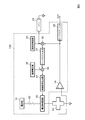
- FIG. 2 is a block diagram for explaining the configuration of the first embodiment of the current sensor according to the present invention.
- FIG. 3 is a diagram for explaining the mounting relationship between the Hall element and the coil in FIG.
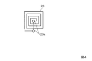
- FIG. 4 is a diagram showing a coil pattern on the substrate in FIG.
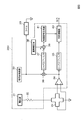
- FIG. 5 is a block diagram for explaining the configuration of a second embodiment of the current sensor according to the present invention.
- FIG. 6 is a block diagram for explaining the configuration of a third embodiment of the current sensor according to the present invention.
- FIG. 7 is a block diagram for explaining the configuration of a fourth embodiment of the current sensor according to the present invention.
- FIG. 2 shows the functional configuration of the first embodiment of the current sensor according to the present invention
- FIG. 3 shows the positional relationship between the Hall elements and the coils.
- the magnetic core 21 through which the magnetic flux generated by the current to be measured is formed is C-shaped or ring-shaped, and the hall element 22 and the coil 23 are arranged in a gap 21a formed in a part thereof. .
- the Hall element 22 outputs an electrical signal corresponding to the applied magnetic flux.
- the coil 23 can apply a magnetic flux to the Hall element 22.
- the hall element 22 and the coil 23 are formed on the same substrate. As shown in FIG. 3, the Hall element 22 is formed on one plate surface of the substrate 24, and the coil 23 is formed on the other plate surface of the substrate 24.
- the coil 23 is a planar coil having a shape as shown in FIG. 4 and is provided in a pattern on the substrate 24.
- reference numeral 23a denotes a via (relay through hole). If the board 24 is a double-sided printed board or a multilayer printed board, such a coil 23 can be easily formed.
- the shape of the coil 23 is not limited to the shape shown in FIG. 4, and may be a spiral shape.
- the electric circuit 100 is provided on the substrate 24.
- the electric circuit 100 has a configuration as shown in FIG. 2.
- the voltage source 31 the resistor 32, the high frequency oscillator 33, the differential amplifier 34, the first low pass filter 35, the multiplier 36, 2 low-pass filter 37, reference voltage source 38, subtractor 39, control signal generator 41, and current control circuit 42.
- the high frequency oscillator 33 applies a high frequency signal to the coil 23.
- the frequency of the high-frequency signal is higher than the output band of the current sensor. For example, when the output band of the current sensor is DC to 100 kHz, the frequency of the high-frequency signal is 1 MHz.
- the voltage source 31 is set to + 5V, for example.
- the hall element 22 outputs an AC voltage having the frequency of the high-frequency signal applied to the coil 23.
- the output of the Hall element 22 is amplified by the differential amplifier 34, and the amplified output is input to the first low-pass filter 35 and the multiplier 36.
- the first low pass filter 35 removes the frequency component of the high frequency signal from the output of the differential amplifier 34. Therefore, the output of the first low-pass filter 35 is zero.
- the output of the differential amplifier 34 input to the multiplier 36 is multiplied with the high frequency signal applied to the coil 23.
- the output of the multiplier 36 is input to the second low-pass filter 37, and the second low-pass filter 37 removes the frequency component of the high-frequency signal from the output of the multiplier 36.
- the output of the second low-pass filter 37 is input to the subtractor 39, and the subtractor 39 subtracts the output of the second low-pass filter 37 from the reference voltage input from the reference voltage source 38.
- the output of the subtractor 39 is a deviation signal from the reference value.
- the deviation signal (output of the subtractor 39) is input to the control signal generator 41.
- the control signal generator 41 is an integrator, and the deviation signal is integrated to generate a control signal.
- the control signal is input to the current control circuit 42, and the current control circuit 42 controls the current supplied to the Hall element 22 by the control signal.
- a transistor can be used for the current control circuit 42.
- the collector current can be controlled by applying a control current to the base, and in the field effect transistor (FET), the drain current can be controlled by applying a control voltage to the gate.
- FET field effect transistor
- the current control circuit 42 operates so as to change the current. For example, when the output of the second low-pass filter 37 is smaller than the reference value, the deviation signal becomes a positive value, and the current control circuit 42 operates to increase the current. Since the Hall element 22 increases in current (drive current), the magnetic sensitivity is increased, so that the output voltage is increased with respect to the magnetic flux from the coil 23 and is controlled so as to approach the reference value, that is, the deviation signal is reduced. Is done.
- the output of the differential amplifier 34 corresponding to the current to be measured is V I sin ( ⁇ 1 t + ⁇ )
- V I amplitude ⁇ 1 : current current angular frequency to be measured
- the output of the corresponding differential amplifier 34 is Asin ⁇ 2 t
- A amplitude ⁇ 2 : high frequency oscillator output angular frequency, high frequency oscillator output, Bsin ⁇ 2 t
- the output of the first and second low-pass filters 35 and 37 will be described as B: amplitude.
- the output of the differential amplifier 34 is V I sin ( ⁇ 1 t + ⁇ ) + Asin ⁇ 2 t It becomes. Since the first low-pass filter 35 removes the frequency component of the high-frequency signal from the output of the differential amplifier 34, the output of the first low-pass filter 35, that is, the output of the current sensor is V I sin ( ⁇ 1 t + ⁇ ) It becomes.
- the second low-pass filter 37 removes a frequency component greater than or equal to
- the output of AB / 2 thus, the value corresponds to the amplitude B of the high-frequency signal output from the high-frequency oscillator 33 and the amplitude A of the output of the differential amplifier 34 corresponding to the high-frequency signal, and this value is controlled to approach the reference value.
- FIG. 5 shows a functional configuration of the current sensor according to the second embodiment of the present invention.
- the arrangement of the Hall element 22 and the coil 23 is the same as in the first embodiment.
- the electric circuit 200 does not have the current control circuit 42 in the electric circuit 100 of the first embodiment, and a variable amplifier 43 is provided in the subsequent stage of the first low-pass filter 35. 1 is the same as the electric circuit 100 of FIG.
- a current (drive current) is supplied from the voltage source 31 to the hall element 22 via the resistor 32.
- the control signal generated by the control signal generator 41 is input to the variable amplifier 43 in this example.
- the gain (gain) of the variable amplifier 43 is controlled by a control signal, and the variable amplifier 43 amplifies the output of the first low-pass filter 35 with the controlled gain. That is, in this example, the control signal is used for gain control of the variable amplifier 43.
- the gain of the variable amplifier 43 is controlled to be small. Therefore, the gain of the variable amplifier 43 can be reduced and compensated by the increase in the magnetic sensitivity of the Hall element 22, whereby the current sensitivity is not affected by the temperature change and is maintained constant. .
- a constant current source may be used in place of the voltage source 31 and the resistor 32. If a constant current source is used, more accurate measurement can be performed.
- Embodiment 3 of the current sensor according to the present invention will be described.
- FIG. 6 shows a functional configuration of the third embodiment, and the electric circuit 100 ′ has a configuration in which a comparator 51 is added to the electric circuit 100 of the first embodiment.
- the comparator 51 receives the control signal generated by the control signal generator 41, and the comparator 51 generates and outputs a failure detection signal from the control signal.
- FIG. 7 shows a functional configuration of a current sensor according to a fourth embodiment of the present invention.
- the electric circuit 200 has a configuration in which a comparator 51 is added to the electric circuit 200 according to the second embodiment.
- the comparator 51 receives a control signal from the control signal generator 41, and the comparator 51 generates and outputs a failure detection signal from the control signal.
- the coil 23 for applying a magnetic flux to the Hall element 22 is a planar coil and is patterned on the substrate 24. Therefore, for example, a troublesome task of winding the coil is unnecessary. In this respect, the current sensor can be manufactured at low cost.
- the control signal generator 41 is an integrator, but may be an amplifier that amplifies the output (deviation signal) of the subtractor 39 to generate a control signal.
Landscapes
- Physics & Mathematics (AREA)
- General Physics & Mathematics (AREA)
- Condensed Matter Physics & Semiconductors (AREA)
- Measuring Instrument Details And Bridges, And Automatic Balancing Devices (AREA)
- Measurement Of Current Or Voltage (AREA)
Abstract
空隙を有し、被測定電流によって発生する磁束を通す磁性体コアと、前記空隙に配置されたホール素子と、ホール素子に磁束を印加するコイルと、コイルに高周波信号を印加する高周波発振器と、ホール素子の出力を増幅する増幅器と、増幅器の出力から高周波信号の周波数成分を除去する第1のローパスフィルタと、増幅器の出力と高周波信号とを掛け算する掛け算器と、掛け算器の出力から高周波信号の周波数と被測定電流の周波数の差以上の周波数成分を除去する第2のローパスフィルタと、基準電圧から第2のローパスフィルタの出力を引き算する引き算器と、引き算器の出力から制御信号を生成する制御信号生成器と、制御信号によりホール素子に供給する電流を制御する電流制御回路とを有する。温度変化の影響を受けず、常に一定の電流感度を得ることができる。
Description
この発明は磁性体コアとホール素子を使用する電流センサに関する。
図1はこの種の電流センサの従来構成例として特許文献1に記載されている電流センサの回路構成を示したものである。この例では電流センサは、磁性体コア1とホール素子2と巻線3と高周波発振器4と増幅回路5とフィルタ6,7と制御回路8とによって構成されている。
被検出電流Iによる周回磁束の磁路をなす磁性体コア1のギャップに配置されたホール素子2は磁束に応じた電気信号を出力する。磁性体コア1には巻線3が巻回されている。高周波発振器4は高周波信号を発生し、巻線3に印加する。高周波信号の周波数は、被検出電流Iの最大周波数の10倍程度またはそれ以上とされている。
ホール素子2により出力された電気信号を増幅する増幅回路5はオペアンプ11を有し、ホール素子2の正側出力端子及び負側出力端子はそれぞれ抵抗Ra,Rbを介してオペアンプ11の正側入力端子及び負側入力端子に接続されている。オペアンプ11の正側入力端子は電源Vccとグランドとの間の抵抗Rc,Rdの直列回路によりバイアスされている。また、抵抗R1,R2の直列回路の一端がオペアンプ11の負側入力端子に接続され、他端がグランドに接続されている。また、抵抗R3の一端が抵抗R1とR2の接続点に接続され、他端がオペアンプ11の出力端子に接続されている。
抵抗R2には制御回路8のトランジスタQのコレクタ-エミッタが並列に接続されており、トランジスタQのコレクタ-エミッタ間の抵抗値を変化させることにより増幅回路5の増幅度が変化する。
フィルタ6は抵抗R4とコンデンサC1で構成されるローパスフィルタであり、増幅回路5の出力信号から高周波信号の周波数と同一の周波数成分を遮断する。増幅回路5の出力信号のうちの被測定電流Iについての周波数成分はフィルタ6を通過し、出力端子に印加される。
フィルタ7はコンデンサC2と抵抗R5で構成されるハイパスフィルタであり、増幅回路5の出力信号から高周波信号の周波数成分と同一の周波数成分を抽出する。フィルタ7を通過した高周波信号についての周波数成分は制御回路8に印加される。
制御回路8はフィルタ7により抽出された電気信号に基づいて、その周波数成分の振幅が所定の一定値になるように増幅回路5の増幅度を制御する。制御回路8は基準電圧Vrefを発生する電源15と、フィルタ7により抽出された周波数成分の電気信号を整流する整流回路16と、整流回路16の出力電圧と基準電圧Vrefとの差に応じた制御信号を出力する比較回路17と、トランジスタQとを有する。
整流回路16はダイオードDとコンデンサC3を有し、比較回路17はオペアンプ18と抵抗R6,R7を有する。比較回路17から出力される制御信号はトランジスタQのエミッタ-ベース間に印加され、制御信号の電圧に応じてコレクタ-エミッタ間の抵抗値が変化するため、増幅回路5の増幅度が変化する。
この電流センサでは高周波発振器4により巻線3に高周波信号が印加される。ホール素子2の出力電圧には高周波信号についての周波数成分と、被検出電流Iについての周波数成分が含まれる。ホール素子2の出力電圧は増幅回路5で増幅され、増幅回路5の出力電圧はフィルタ6及び7に印加される。被検出電流Iについての周波数成分はフィルタ6を通過し、電流センサの出力電圧Voutとして出力端子に印加される。
一方、高周波信号についての周波数成分はフィルタ7を通過し、制御回路8に印加される。制御回路8では整流回路16によりその高周波信号についての周波数成分が整流平滑化され、比較回路17により整流回路16の出力電圧と基準電圧Vrefとが比較され、両者の差が所定の値に近づくようにトランジスタQが制御される。
従って、この電流センサでは高周波信号についての周波数成分のみを整流平滑化して得られる直流電圧が所定の一定値になるように、増幅回路5の増幅度が常時制御されるものとなっている。これにより、被検出電流Iとは別に印加される高周波信号についての検出値も様々な誤差要因に起因して誤差を含んでいるが、その誤差を無くすべく増幅回路5の増幅度が調整されるため、被検出電流Iについての誤差も併せて低減されるものとなっている。
ところで、ホール素子を使用する電流センサでは、ホール素子の磁気感度が温度によって変化することに基因して電流感度が温度によって変化するという問題があり、このような電流感度の温度依存性を補償することは高精度な測定を行う上で重要な課題となっている。
この点、上述した特許文献1に記載されている電流センサは、ホール素子の磁気感度の温度依存性に対しては補償を行うことができるものとなっているものの、電流センサ全体として見た場合、電流感度の温度依存性に対する補償は十分とは言えず、測定誤差が生じうるものとなっていた。
即ち、特許文献1に記載されている電流センサは、ホール素子2の出力電圧を増幅する増幅回路5の増幅度を制御する制御回路8において、その制御回路8内の整流回路16にダイオードDを用いている。ダイオードDは温度変化、経年変化により順方向降下電圧Vfが変化するため、精度が悪く、その点で電流感度の温度依存性に対する補償は十分とは言えないものとなっていた。
この発明の目的は、ホール素子の磁気感度の温度依存性の影響を排除し、温度が変化しても常に一定の電流感度が得られるようにした温度依存性のない高精度な電流センサを提供することにある。
この発明の第1の観点によれば、電流センサは、空隙を有し、被測定電流によって発生する磁束を通す磁性体コアと、前記空隙に配置されたホール素子と、ホール素子に磁束を印加するコイルと、コイルに高周波信号を印加する高周波発振器と、ホール素子の出力を増幅する増幅器と、増幅器の出力から前記高周波信号の周波数成分を除去する第1のローパスフィルタと、増幅器の出力と前記高周波信号とを掛け算する掛け算器と、掛け算器の出力から前記高周波信号の周波数と被測定電流の周波数の差以上の周波数成分を除去する第2のローパスフィルタと、基準電圧から第2のローパスフィルタの出力を引き算する引き算器と、引き算器の出力から制御信号を生成する制御信号生成器と、前記制御信号によりホール素子に供給する電流を制御する電流制御回路とを有する。
この発明の第2の観点によれば、電流センサは、空隙を有し、被測定電流によって発生する磁束を通す磁性体コアと、前記空隙に配置されたホール素子と、ホール素子に磁束を印加するコイルと、コイルに高周波信号を印加する高周波発振器と、ホール素子の出力を増幅する増幅器と、増幅器の出力から前記高周波信号の周波数成分を除去する第1のローパスフィルタと、増幅器の出力と前記高周波信号とを掛け算する掛け算器と、掛け算器の出力から前記高周波信号の周波数と被測定電流の周波数の差以上の周波数成分を除去する第2のローパスフィルタと、基準電圧から第2のローパスフィルタの出力を引き算する引き算器と、引き算器の出力から制御信号を生成する制御信号生成器と、前記制御信号によりゲインが制御され、その制御されたゲインで第1のローパスフィルタの出力を増幅する可変増幅器とを有する。
この発明によれば、電流感度は温度変化の影響を受けず、常に一定に制御されるため、温度特性に優れた高精度な電流センサを得ることができる。
以下にこの発明の実施例を説明する。
図2はこの発明による電流センサの実施例1の機能構成を示したものであり、図3はホール素子及びコイルの配置関係を示したものである。
被測定電流によって発生する磁束を通す磁性体コア21は図3に示したようにC形あるいはリング形状とされ、その一部に形成された空隙21aにホール素子22とコイル23が配置されている。ホール素子22は印加される磁束に応じた電気信号を出力する。コイル23はホール素子22に磁束を印加することができるものとなっている。
ホール素子22とコイル23はこの例では同一基板上に形成されている。ホール素子22は図3に示したように基板24の一方の板面に形成され、コイル23は基板24の他方の板面に形成されている。
コイル23は図4に示したような形状を有する平面コイルとされ、基板24上にパターン形成されて設けられている。図4中、23aはビア(中継スルーホール)を示す。基板24を両面プリント基板もしくは多層プリント基板とすれば、このようなコイル23を容易に形成することができる。なお、コイル23の形状は図4に示したような形状に限らず、渦巻形状としてもよい。
基板24上には電気回路100が設けられている。電気回路100は図2に示したような構成を有するものとされ、この例では電圧源31と抵抗器32と高周波発振器33と差動増幅器34と第1のローパスフィルタ35と掛け算器36と第2のローパスフィルタ37と基準電圧源38と引き算器39と制御信号生成器41と電流制御回路42とによって構成されている。
高周波発振器33はコイル23に高周波信号を印加する。この高周波信号の周波数は電流センサの出力帯域よりも高い周波数とされる。例えば、電流センサの出力帯域をDC~100kHzとした場合、高周波信号の周波数は1MHzとされる。
今、被測定電流が0と仮定して電気回路100の動作を説明する。
電圧源31から抵抗器32及び電流制御回路42を介してホール素子22に電流(駆動電流)が供給される。電圧源31は例えば+5Vとされる。
ホール素子22からはコイル23に印加された高周波信号の周波数の交流電圧が出力される。ホール素子22の出力は差動増幅器34で増幅され、増幅された出力は第1のローパスフィルタ35と掛け算器36に入力される。第1のローパスフィルタ35は差動増幅器34の出力から高周波信号の周波数成分を除去する。よって、第1のローパスフィルタ35の出力は0となる。
一方、掛け算器36に入力された差動増幅器34の出力は、コイル23に印加されている高周波信号と掛け算される。掛け算器36の出力は第2のローパスフィルタ37に入力され、第2のローパスフィルタ37は掛け算器36の出力から高周波信号の周波数成分を除去する。
第2のローパスフィルタ37の出力は引き算器39に入力され、引き算器39は基準電圧源38から入力される基準電圧から第2のローパスフィルタ37の出力を引き算する。引き算器39の出力は基準値との偏差信号となる。
偏差信号(引き算器39の出力)は制御信号生成器41に入力される。制御信号生成器41はこの例では積分器とされ、偏差信号は積分されて制御信号が生成される。制御信号は電流制御回路42に入力され、電流制御回路42は制御信号によりホール素子22に供給する電流を制御する。
電流制御回路42には例えばトランジスタを用いることができる。バイポーラトランジスタでは、ベースに制御電流を印加することでコレクタ電流を制御することができ、電界効果トランジスタ(FET)では、ゲートに制御電圧を印加することでドレイン電流を制御することができる。
電流制御回路42は電流を変化させるように動作する。例えば、第2のローパスフィルタ37の出力が基準値より小さい場合、偏差信号は正の値となり、電流制御回路42は電流を大きくするように動作する。ホール素子22は電流(駆動電流)が増加するので磁気感度が大きくなり、よってコイル23からの磁束に対して出力電圧が大きくなり、基準値に近づくように、つまり偏差信号が小さくなるように制御される。
このような制御により、例えば温度変化によってホール素子22の磁気感度が変化すると、ホール素子22から出力される高周波信号の振幅が変化し、それを補償するようにホール素子22の磁気感度が制御されるため、電流センサの電流感度は温度変化の影響を受けず、常に一定の電流感度が維持される。
以下、被測定電流に対応する差動増幅器34の出力を、
VIsin(ω1t+φ)
但し、VI:振幅
ω1:被測定電流角周波数
φ:高周波発振器出力に対する位相差
とし(被測定電流が直流の場合はω1=0,φ=0)、コイル23によって印加される磁束に対応する差動増幅器34の出力を、
Asinω2t
但し、A:振幅
ω2:高周波発振器出力角周波数
とし、高周波発振器出力を、
Bsinω2t
但し、B:振幅
として、第1及び第2のローパスフィルタ35,37の出力を説明する。
VIsin(ω1t+φ)
但し、VI:振幅
ω1:被測定電流角周波数
φ:高周波発振器出力に対する位相差
とし(被測定電流が直流の場合はω1=0,φ=0)、コイル23によって印加される磁束に対応する差動増幅器34の出力を、
Asinω2t
但し、A:振幅
ω2:高周波発振器出力角周波数
とし、高周波発振器出力を、
Bsinω2t
但し、B:振幅
として、第1及び第2のローパスフィルタ35,37の出力を説明する。
差動増幅器34の出力は、
VIsin(ω1t+φ)+Asinω2t
となる。第1のローパスフィルタ35は差動増幅器34の出力から高周波信号の周波数成分を除去するので第1のローパスフィルタ35の出力、即ち電流センサの出力は、
VIsin(ω1t+φ)
となる。一方、掛け算器36の出力は、
{VIsin(ω1t+φ)+Asinω2t}×Bsinω2t
=VIBsin(ω1t+φ)×sinω2t+ABsinω2t×sinω2t
=VIB{cos((ω1-ω2)t+φ)-cos((ω1+ω2)t+φ)}/2+AB(1-cos2ω2t)/2
となる。第2のローパスフィルタ37は掛け算器36の出力から|ω1-ω2|以上、即ち高周波信号の周波数と被測定電流の周波数の差以上の周波数成分を除去するので、第2のローパスフィルタ37の出力は、
AB/2
となり、高周波発振器33から出力される高周波信号の振幅B及び高周波信号に対応する差動増幅器34の出力の振幅Aに対応した値となり、この値が基準値に近づくように制御される。
VIsin(ω1t+φ)+Asinω2t
となる。第1のローパスフィルタ35は差動増幅器34の出力から高周波信号の周波数成分を除去するので第1のローパスフィルタ35の出力、即ち電流センサの出力は、
VIsin(ω1t+φ)
となる。一方、掛け算器36の出力は、
{VIsin(ω1t+φ)+Asinω2t}×Bsinω2t
=VIBsin(ω1t+φ)×sinω2t+ABsinω2t×sinω2t
=VIB{cos((ω1-ω2)t+φ)-cos((ω1+ω2)t+φ)}/2+AB(1-cos2ω2t)/2
となる。第2のローパスフィルタ37は掛け算器36の出力から|ω1-ω2|以上、即ち高周波信号の周波数と被測定電流の周波数の差以上の周波数成分を除去するので、第2のローパスフィルタ37の出力は、
AB/2
となり、高周波発振器33から出力される高周波信号の振幅B及び高周波信号に対応する差動増幅器34の出力の振幅Aに対応した値となり、この値が基準値に近づくように制御される。
図5はこの発明による電流センサの実施例2の機能構成を示したものである。ホール素子22及びコイル23の配置は実施例1と同じである。
この例では電気回路200は実施例1の電気回路100中の電流制御回路42がなく、第1のローパスフィルタ35の後段に可変増幅器43を設けたものとなっており、他の構成は実施例1の電気回路100と同じである。ホール素子22には電圧源31から抵抗器32を介して電流(駆動電流)が供給される。
実施例1と同様にして、制御信号生成器41で生成される制御信号は、この例では可変増幅器43に入力される。可変増幅器43のゲイン(利得)は制御信号により制御され、その制御されたゲインで可変増幅器43は第1のローパスフィルタ35の出力を増幅する。即ち、この例では制御信号は可変増幅器43のゲイン制御に使用される。
例えば、ホール素子22の磁気感度が温度変化で大きくなった場合、引き算器39から出力される偏差信号は負となり、制御信号生成器41で生成される制御信号も負となる。この時、可変増幅器43のゲインは小さくなるように制御される。よって、ホール素子22の磁気感度が大きくなった分、可変増幅器43のゲインが小さくなって補償することができ、これにより電流感度は温度変化の影響を受けず、一定に維持されるものとなる。
なお、この例では電圧源31及び抵抗器32に替えて定電流源を用いるようにしてもよく、定電流源を用いれば、より高精度な測定を行うことができる。
次に、この発明による電流センサの実施例3の構成について説明する。
図6は実施例3の機能構成を示したものであり、電気回路100’は実施例1の電気回路100に比較器51が付加された構成となっている。比較器51には制御信号生成器41で生成される制御信号が入力され、比較器51はその制御信号から故障検出信号を生成して出力する。
電圧源31、抵抗器32、電流制御回路42、ホール素子22、差動増幅器34、掛け算器36、第2のローパスフィルタ37、基準電圧源38、引き算器39、制御信号生成器41、高周波発振器33及びコイル23のいずれかが故障した場合、積分器で構成されている制御信号生成器41から出力される制御信号は0又は電源電圧に飽和する。よって、この場合の比較器51の出力が例えば0になるように、比較器51をウインドコンパレータで構成すれば、故障検出を行うことができる。
図7はこの発明による電流センサの実施例4の機能構成を示したものであり、電気回路200’は実施例2の電気回路200に比較器51が付加された構成となっている。比較器51には実施例3と同様、制御信号生成器41から制御信号が入力され、比較器51はその制御信号から故障検出信号を生成して出力する。
電圧源31、抵抗器32、ホール素子22、差動増幅器34、掛け算器36、第2のローパスフィルタ37、基準電圧源38、引き算器39、制御信号生成器41、高周波発振器33及びコイル23のいずれかが故障した場合、実施例3と同様、制御信号は0又は電源電圧に飽和するため、この場合の比較器51の出力が例えば0になるように比較器51をウインドコンパレータで構成すれば、故障検出を行うことができる。
以上、各種実施例について説明したが、ホール素子22に磁束を印加するコイル23は平面コイルとされ、基板24上にパターン形成されるため、例えばコイルを巻くといった面倒な作業は不要であり、その点で電流センサを低コストで製作することができる。
なお、制御信号生成器41は積分器としているが、引き算器39の出力(偏差信号)を増幅して制御信号を生成する増幅器としてもよい。
Claims (6)
- 空隙を有し、被測定電流によって発生する磁束を通す磁性体コアと、
前記空隙に配置されたホール素子と、
前記ホール素子に磁束を印加するコイルと、
前記コイルに高周波信号を印加する高周波発振器と、
前記ホール素子の出力を増幅する増幅器と、
前記増幅器の出力から前記高周波信号の周波数成分を除去する第1のローパスフィルタと、
前記増幅器の出力と前記高周波信号とを掛け算する掛け算器と、
前記掛け算器の出力から前記高周波信号の周波数と前記被測定電流の周波数の差以上の周波数成分を除去する第2のローパスフィルタと、
基準電圧から前記第2のローパスフィルタの出力を引き算する引き算器と、
前記引き算器の出力から制御信号を生成する制御信号生成器と、
前記制御信号により前記ホール素子に供給する電流を制御する電流制御回路とを有する電流センサ。 - 空隙を有し、被測定電流によって発生する磁束を通す磁性体コアと、
前記空隙に配置されたホール素子と、
前記ホール素子に磁束を印加するコイルと、
前記コイルに高周波信号を印加する高周波発振器と、
前記ホール素子の出力を増幅する増幅器と、
前記増幅器の出力から前記高周波信号の周波数成分を除去する第1のローパスフィルタと、
前記増幅器の出力と前記高周波信号とを掛け算する掛け算器と、
前記掛け算器の出力から前記高周波信号の周波数と前記被測定電流の周波数の差以上の周波数成分を除去する第2のローパスフィルタと、
基準電圧から前記第2のローパスフィルタの出力を引き算する引き算器と、
前記引き算器の出力から制御信号を生成する制御信号生成器と、
前記制御信号によりゲインが制御され、その制御されたゲインで前記第1のローパスフィルタの出力を増幅する可変増幅器とを有する電流センサ。 - 請求項1又は2の電流センサにおいて、
前記制御信号から故障検出信号を生成する比較器を有する。 - 請求項1乃至3のいずれかの電流センサにおいて、
前記ホール素子と前記コイルは同一基板上に形成されている。 - 請求項1乃至4のいずれかの電流センサにおいて、
前記制御信号生成器は積分器である。 - 請求項1乃至4のいずれかの電流センサにおいて、
前記制御信号生成器は増幅器である。
Applications Claiming Priority (2)
| Application Number | Priority Date | Filing Date | Title |
|---|---|---|---|
| JP2013124606 | 2013-06-13 | ||
| JP2013-124606 | 2013-06-13 |
Publications (1)
| Publication Number | Publication Date |
|---|---|
| WO2014199654A1 true WO2014199654A1 (ja) | 2014-12-18 |
Family
ID=52021963
Family Applications (1)
| Application Number | Title | Priority Date | Filing Date |
|---|---|---|---|
| PCT/JP2014/052056 Ceased WO2014199654A1 (ja) | 2013-06-13 | 2014-01-30 | 電流センサ |
Country Status (1)
| Country | Link |
|---|---|
| WO (1) | WO2014199654A1 (ja) |
Cited By (2)
| Publication number | Priority date | Publication date | Assignee | Title |
|---|---|---|---|---|
| CN109030906A (zh) * | 2017-06-09 | 2018-12-18 | 北京普源精电科技有限公司 | 一种电流探头 |
| CN111508686A (zh) * | 2020-04-14 | 2020-08-07 | 北京动力源新能源科技有限责任公司 | 滤波电感、滤波器及基于滤波电感进行电流采样的方法 |
Citations (6)
| Publication number | Priority date | Publication date | Assignee | Title |
|---|---|---|---|---|
| JPS51117080A (en) * | 1975-04-07 | 1976-10-14 | Ricoh Co Ltd | Magnetic field measuring method using hall element |
| JPH1174823A (ja) * | 1997-08-28 | 1999-03-16 | Kokusai Electric Co Ltd | 非接触icカードシステム |
| JPH11281678A (ja) * | 1998-03-30 | 1999-10-15 | Shimadzu Corp | 電流センサ |
| JP2000055999A (ja) * | 1998-08-11 | 2000-02-25 | Tdk Corp | 磁気センサ装置および電流センサ装置 |
| JP2006126012A (ja) * | 2004-10-28 | 2006-05-18 | Asahi Kasei Microsystems Kk | 磁電変換システム及び磁電変換装置並びにその制御回路 |
| JP2012008009A (ja) * | 2010-06-24 | 2012-01-12 | Sumida Corporation | 電流センサ |
-
2014
- 2014-01-30 WO PCT/JP2014/052056 patent/WO2014199654A1/ja not_active Ceased
Patent Citations (6)
| Publication number | Priority date | Publication date | Assignee | Title |
|---|---|---|---|---|
| JPS51117080A (en) * | 1975-04-07 | 1976-10-14 | Ricoh Co Ltd | Magnetic field measuring method using hall element |
| JPH1174823A (ja) * | 1997-08-28 | 1999-03-16 | Kokusai Electric Co Ltd | 非接触icカードシステム |
| JPH11281678A (ja) * | 1998-03-30 | 1999-10-15 | Shimadzu Corp | 電流センサ |
| JP2000055999A (ja) * | 1998-08-11 | 2000-02-25 | Tdk Corp | 磁気センサ装置および電流センサ装置 |
| JP2006126012A (ja) * | 2004-10-28 | 2006-05-18 | Asahi Kasei Microsystems Kk | 磁電変換システム及び磁電変換装置並びにその制御回路 |
| JP2012008009A (ja) * | 2010-06-24 | 2012-01-12 | Sumida Corporation | 電流センサ |
Cited By (2)
| Publication number | Priority date | Publication date | Assignee | Title |
|---|---|---|---|---|
| CN109030906A (zh) * | 2017-06-09 | 2018-12-18 | 北京普源精电科技有限公司 | 一种电流探头 |
| CN111508686A (zh) * | 2020-04-14 | 2020-08-07 | 北京动力源新能源科技有限责任公司 | 滤波电感、滤波器及基于滤波电感进行电流采样的方法 |
Similar Documents
| Publication | Publication Date | Title |
|---|---|---|
| JP5004368B2 (ja) | 電流センサ | |
| CN106574950B (zh) | 具有磁通门检测器的电流变换器 | |
| TWI426693B (zh) | 切換式電源供應器及其控制電路與控制方法 | |
| CN101622777B (zh) | 电能转换器中的负载电流检测 | |
| US9383392B2 (en) | Current sensor | |
| JP2017521675A5 (ja) | ||
| CN110088636B (zh) | 具有磁通门的电流传感器 | |
| JP5804318B2 (ja) | 電流センサ | |
| JP2012225664A (ja) | 電流センサ及び電流検出方法 | |
| WO2014199654A1 (ja) | 電流センサ | |
| JP6728777B2 (ja) | 電流検知装置 | |
| JP2005521048A (ja) | 発振器により給電されるセンサの出力電圧を整流するための回路装置 | |
| CN112230035B (zh) | 电流互感器 | |
| JP2018093574A (ja) | 交流電流検出回路 | |
| JP2001033533A (ja) | 磁気インピーダンスセンサ回路 | |
| JP3583699B2 (ja) | センサ装置 | |
| JP2017203732A (ja) | 電圧測定装置 | |
| JP7568773B1 (ja) | 電流測定装置および電流測定方法 | |
| JP3208429B2 (ja) | 復調器およびそれを用いた変位測定器 | |
| JP2526597Y2 (ja) | 差動変圧器型変位検出器 | |
| JP2020041945A (ja) | 磁界検出センサ | |
| JP2017194419A (ja) | 電圧測定装置 | |
| JP2006136037A (ja) | インバータ出力電圧の直流成分検出回路 | |
| JP5970847B2 (ja) | 圧電トランスを用いた電源装置 | |
| JPH0120647Y2 (ja) |
Legal Events
| Date | Code | Title | Description |
|---|---|---|---|
| 121 | Ep: the epo has been informed by wipo that ep was designated in this application |
Ref document number: 14811074 Country of ref document: EP Kind code of ref document: A1 |
|
| NENP | Non-entry into the national phase |
Ref country code: DE |
|
| 122 | Ep: pct application non-entry in european phase |
Ref document number: 14811074 Country of ref document: EP Kind code of ref document: A1 |