WO2014185208A1 - 電荷輸送性ワニス - Google Patents
電荷輸送性ワニス Download PDFInfo
- Publication number
- WO2014185208A1 WO2014185208A1 PCT/JP2014/060823 JP2014060823W WO2014185208A1 WO 2014185208 A1 WO2014185208 A1 WO 2014185208A1 JP 2014060823 W JP2014060823 W JP 2014060823W WO 2014185208 A1 WO2014185208 A1 WO 2014185208A1
- Authority
- WO
- WIPO (PCT)
- Prior art keywords
- group
- carbon atoms
- substituted
- bis
- charge transporting
- Prior art date
- Legal status (The legal status is an assumption and is not a legal conclusion. Google has not performed a legal analysis and makes no representation as to the accuracy of the status listed.)
- Ceased
Links
Classifications
-
- C—CHEMISTRY; METALLURGY
- C07—ORGANIC CHEMISTRY
- C07D—HETEROCYCLIC COMPOUNDS
- C07D519/00—Heterocyclic compounds containing more than one system of two or more relevant hetero rings condensed among themselves or condensed with a common carbocyclic ring system not provided for in groups C07D453/00 or C07D455/00
-
- C—CHEMISTRY; METALLURGY
- C07—ORGANIC CHEMISTRY
- C07D—HETEROCYCLIC COMPOUNDS
- C07D333/00—Heterocyclic compounds containing five-membered rings having one sulfur atom as the only ring hetero atom
- C07D333/02—Heterocyclic compounds containing five-membered rings having one sulfur atom as the only ring hetero atom not condensed with other rings
- C07D333/04—Heterocyclic compounds containing five-membered rings having one sulfur atom as the only ring hetero atom not condensed with other rings not substituted on the ring sulphur atom
- C07D333/26—Heterocyclic compounds containing five-membered rings having one sulfur atom as the only ring hetero atom not condensed with other rings not substituted on the ring sulphur atom with hetero atoms or with carbon atoms having three bonds to hetero atoms with at the most one bond to halogen, e.g. ester or nitrile radicals, directly attached to ring carbon atoms
- C07D333/30—Hetero atoms other than halogen
- C07D333/32—Oxygen atoms
-
- H—ELECTRICITY
- H01—ELECTRIC ELEMENTS
- H01B—CABLES; CONDUCTORS; INSULATORS; SELECTION OF MATERIALS FOR THEIR CONDUCTIVE, INSULATING OR DIELECTRIC PROPERTIES
- H01B1/00—Conductors or conductive bodies characterised by the conductive materials; Selection of materials as conductors
- H01B1/06—Conductors or conductive bodies characterised by the conductive materials; Selection of materials as conductors mainly consisting of other non-metallic substances
- H01B1/12—Conductors or conductive bodies characterised by the conductive materials; Selection of materials as conductors mainly consisting of other non-metallic substances organic substances
- H01B1/124—Intrinsically conductive polymers
- H01B1/127—Intrinsically conductive polymers comprising five-membered aromatic rings in the main chain, e.g. polypyrroles, polythiophenes
-
- H—ELECTRICITY
- H10—SEMICONDUCTOR DEVICES; ELECTRIC SOLID-STATE DEVICES NOT OTHERWISE PROVIDED FOR
- H10K—ORGANIC ELECTRIC SOLID-STATE DEVICES
- H10K50/00—Organic light-emitting devices
- H10K50/10—OLEDs or polymer light-emitting diodes [PLED]
- H10K50/14—Carrier transporting layers
- H10K50/15—Hole transporting layers
-
- H—ELECTRICITY
- H10—SEMICONDUCTOR DEVICES; ELECTRIC SOLID-STATE DEVICES NOT OTHERWISE PROVIDED FOR
- H10K—ORGANIC ELECTRIC SOLID-STATE DEVICES
- H10K85/00—Organic materials used in the body or electrodes of devices covered by this subclass
- H10K85/10—Organic polymers or oligomers
- H10K85/111—Organic polymers or oligomers comprising aromatic, heteroaromatic, or aryl chains, e.g. polyaniline, polyphenylene or polyphenylene vinylene
- H10K85/113—Heteroaromatic compounds comprising sulfur or selene, e.g. polythiophene
Definitions
- the present invention relates to a charge transporting varnish, and more specifically, to a charge transporting varnish containing a charge transporting material composed of a predetermined thiophene derivative, a dopant material composed of a heteropoly acid, and an organic solvent.
- organic electroluminescence (hereinafter also referred to as organic EL) element a charge transporting thin film made of an organic compound is used as a light emitting layer or a charge injection layer.
- This coloring of the charge transporting thin film is known to reduce the color purity and color reproducibility of the organic EL device.
- coloring becomes a problem in various full-color technologies for organic EL displays such as a three-color light emission method, a white color method, and a color conversion method, and becomes a significant obstacle in stably producing organic EL elements.
- the charge transporting thin film of the organic EL element is desired to have a high transmittance in the visible region and to have a high transparency.
- a charge transporting material that can be applied and that provides a thin film with excellent transparency that can realize excellent EL element characteristics when applied to a hole injection layer of an organic EL element has been developed (see Patent Document 1). .
- the present invention provides a charge transporting thin film that has high transparency and can realize excellent luminance characteristics and high durability when used as a hole injection layer of an organic EL element, as in the technique of Patent Document 1.
- An object is to provide a charge transporting varnish.
- Patent Document 2 does not specifically disclose a varnish using an oligothiophene derivative and a heteropolyacid.
- a charge transporting varnish comprising a charge transporting material comprising an oligothiophene derivative represented by formula (1), a dopant material comprising a heteropolyacid, and an organic solvent;
- R 1 to R 4 are each independently a hydrogen atom, an alkyl group having 1 to 20 carbon atoms that may be substituted with Z 1 , or 2 to C carbon atoms that may be substituted with Z 1
- 20 alkenyl group Z 1 at carbon atoms which may be substituted have 2-20 alkynyl group
- aryl group Z 2 are carbon atoms that may 6 to be 20 substituted by, may be substituted with Z 2
- R 1 and R 2 are an alkyl group having 1 to 20
- n 1 to n 3 independently represent a natural number and satisfy 4 ⁇ n 1 + n 2 + n 3 ⁇ 20.
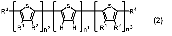
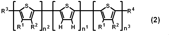
- the oligothiophene derivative is a charge transporting varnish represented by formula (2): (Wherein R 1 to R 4 and n 1 to n 3 have the same meaning as described above.) 3.
- the method for producing an organic electroluminescence device is characterized in that the charge transporting thin film is used.
- the charge transporting varnish of the present invention By using the charge transporting varnish of the present invention, a highly transparent charge transporting thin film with suppressed absorption in the visible region can be obtained. By using this thin film, it is possible to ensure the color reproducibility of the element without degrading the color purity of the electroluminescent light or the light transmitted through the color filter. This can greatly contribute to the improvement of efficiency, and it is possible to reduce the size of the organic EL element and reduce the driving voltage.
- a charge transporting varnish of the present invention a charge transporting thin film having high transparency and conductivity can be obtained. By applying this thin film to a hole injection layer of an organic EL device, high light emission is obtained. An organic EL device having efficiency and excellent durability can be obtained.
- the charge transporting varnish of the present invention can produce a thin film excellent in charge transporting properties with good reproducibility even when using various wet processes capable of forming a film over a large area such as a spin coating method or a slit coating method. It can sufficiently cope with recent progress in the field of organic EL elements.
- the thin film obtained from the charge transporting varnish of the present invention can be used as an antistatic film, an anode buffer layer of an organic thin film solar cell, or the like.
- the charge transporting varnish according to the present invention includes a charge transporting material composed of an oligothiophene derivative represented by the formula (1), a dopant material composed of a heteropolyacid, and an organic solvent.
- the charge transportability is synonymous with conductivity and is synonymous with hole transportability.
- the charge transporting substance itself may be charge transporting, or may be charge transporting when used with an electron accepting substance.
- the charge transporting varnish may itself have a charge transporting property, and the resulting solid film may have a charge transporting property.
- R 1 - R 4 are each independently a hydrogen atom, an alkyl group which have 1 to 20 carbon atoms that may substituted with Z 1, carbon atoms, which may be substituted with Z 1 2-20 alkenyl group, an alkynyl group which have 2-20 carbon atoms substituted with Z 1, aryl group Z 2 is optionally 6 to carbon atoms which may be 20 substituted with, it is substituted with Z 2
- a C2-C20 heteroaryl group, -OY 1 group, -SY 2 group, -NHY 3 , -NY 4 Y 5 group, -NHC (O) Y 6 group, or 4- (diphenylamino) phenyl Y 1 to Y 6 each independently represents an alkyl group having 1 to 20 carbon atoms which may be substituted with Z 1 , or an alkenyl group having 2 to 20 carbon atoms which may be substituted with Z 1 group, an alkynyl group which have 2-20 carbon atoms substituted with Z
- the alkyl group having 1 to 20 carbon atoms may be linear, branched, or cyclic.
- alkenyl group having 2 to 20 carbon atoms include ethenyl group, n-1-propenyl group, n-2-propenyl group, 1-methylethenyl group, n-1-butenyl group, n-2-butenyl group, n-3-butenyl group, 2-methyl-1-propenyl group, 2-methyl-2-propenyl group, 1-ethylethenyl group, 1-methyl-1-propenyl group, 1-methyl-2-propenyl group, n- 1-pentenyl group, n-1-decenyl group, n-1-eicocenyl group and the like can be mentioned.
- alkynyl group having 2 to 20 carbon atoms examples include ethynyl group, n-1-propynyl group, n-2-propynyl group, n-1-butynyl group, n-2-butynyl group, and n-3-butynyl.
- aryl group having 6 to 20 carbon atoms include phenyl group, 1-naphthyl group, 2-naphthyl group, 1-anthryl group, 2-anthryl group, 9-anthryl group, 1-phenanthryl group, 2-phenanthryl group. Group, 3-phenanthryl group, 4-phenanthryl group, 9-phenanthryl group and the like.
- heteroaryl group having 2 to 20 carbon atoms examples include 2-thienyl, 3-thienyl, 2-furanyl, 3-furanyl, 2-oxazolyl, 4-oxazolyl, 5-oxazolyl, 3-isoxazolyl, 4-isoxazolyl. , 5-isoxazolyl, 2-thiazolyl, 4-thiazolyl, 5-thiazolyl, 3-isothiazolyl, 4-isothiazolyl, 5-isothiazolyl, 2-imidazolyl, 4-imidazolyl, 2-pyridyl, 3-pyridyl, 4-pyridyl group, etc. Is mentioned.
- suitable oligothiophene derivatives include, for example, those represented by the formula (2).
- R 1 and R 2 good hydrogen atom, optionally substituted with an alkyl group or Z 1, of is 1 carbon atoms which may be ⁇ 20 substituted by Z 1 carbon number preferably from 1 to alkyloxy group 20 (-OY 1 group is Y 1 is an alkyl group which 1 carbon atoms which may be ⁇ 20 substituted by Z 1), a hydrogen atom, optionally substituted by Z 1 A preferable alkyl group having 1 to 10 carbon atoms or an alkyloxy group having 1 to 10 carbon atoms which may be substituted with Z 1 is more preferable, and a hydrogen atom or carbon atoms having 1 to 8 which may be substituted with Z 1 Or an alkyloxy group having 1 to 8 carbon atoms which may be substituted with Z 1 is even more preferable.
- the R 3 and R 4 a hydrogen atom, Z 1 carbon atoms which may be substituted dialkylamino group (Y 4 and Y 5 of is 1-2 carbon atoms which may be 40 substituted by Z 1 in 1 -NY 4 Y 5 group which is an alkyl group of ⁇ 20), a diarylamino group having 12 to 40 carbon atoms which may be substituted with Z 2 (carbons where Y 4 and Y 5 may be substituted with Z 2) -NY 4 Y 5 group which is an aryl group of 6 to 20) or 4- (diphenylamino) phenyl group is preferable, and a dialkylamino group having 2 to 20 carbon atoms which may be substituted with a hydrogen atom or Z 1 A diarylamino group having 12 to 20 carbon atoms which may be substituted with Z 2 , or a 4- (diphenylamino) phenyl group which is optionally substituted with Z 2 , and has 12 to 40 carbon atoms which may be
- n 1 to n 3 each independently represent a natural number and satisfy 4 ⁇ n 1 + n 2 + n 3 ⁇ 20, but n 1 is preferably 1 to 15, more preferably 1 to 10, More preferably, it is 2 to 5, and more preferably 2 to 3.
- n 2 and n 3 are preferably 1 to 15, more preferably 1 to 10, still more preferably 1 to 5, and still more preferably 1 to 3.
- n 1 to n 3 are preferably n 1 + n 2 + n 3 ⁇ 8, more preferably n 1 + n 2 + n 3 ⁇ 7, and much more.
- it satisfies n 1 + n 2 + n 3 ⁇ 6, more preferably n 1 + n 2 + n 3 ⁇ 5.
- the alkyl group, alkenyl group and alkynyl group of R 1 to R 4 and Y 1 to Y 6 are substituted with Z 1 which is an aryl group having 6 to 20 carbon atoms or a heteroaryl group having 2 to 20 carbon atoms.
- the aryl group and heteroaryl group of R 1 to R 10 and Y 1 to Y 6 may be an alkyl group having 1 to 20 carbon atoms, an alkenyl group having 2 to 20 carbon atoms, or an alkynyl group having 2 to 20 carbon atoms. May be substituted with Z 2 .
- Z 1 is preferably an aryl group having 6 to 20 carbon atoms, more preferably a phenyl group, and most preferably not present (that is, unsubstituted). It is.
- Z 2 is preferably an alkyl group having 1 to 20 carbon atoms, more preferably an alkyl group having 1 to 10 carbon atoms, still more preferably an alkyl group having 1 to 8 carbon atoms, and an alkyl group having 1 to 6 carbon atoms. Is more preferred and is optimally absent (ie, unsubstituted).
- the oligothiophene derivative used in the present invention is synthesized by a known method (for example, a method described in JP-A No. 02-250881 or Chem. Eur. J., 2005, 11, pp. 3742-3752). Alternatively, a commercially available product may be used. That is, the oligothiophene derivative used in the present invention can be specifically synthesized by, for example, the following schemes 1 and 2, and in particular, at both ends, an alkyl group, an alkenyl group, an alkynyl group, an aryl group Alternatively, an oligothiophene derivative (formula (1 ′)) having a heteroaryl group can also be synthesized according to Scheme 3 below.
- Hal represents a halogen atom or a pseudohalogen group
- R 1 to R 4 and n 1 to n 3 have the same meaning as described above
- n Bu represents an n-butyl group.
- halogen atom examples include a fluorine atom, a chlorine atom, a bromine atom, and an iodine atom.
- pseudohalogen groups include (fluoro) alkylsulfonyloxy groups such as methanesulfonyloxy group, trifluoromethanesulfonyloxy group, and nonafluorobutanesulfonyloxy group; aromatic sulfonyloxy groups such as benzenesulfonyloxy group and toluenesulfonyloxy group Is mentioned.
- R 5 and R 6 independently of one another, an alkenyl group of an alkyl group, carbon atoms which may be substituted with Z 1 2 to 20 of to 1 carbon atoms which may be ⁇ 20 substituted with Z 1, Z 1 in substituted 2 carbon atoms which may be 1-20 alkynyl group, aryl group Z 2 are carbon atoms 6 also be ⁇ 20 substituted by or Z 2 which may be 2 to 20 carbon atoms substituted with, Represents a heteroaryl group, and specific examples of these alkyl group, alkenyl group, alkynyl group, aryl group and heteroaryl group include the same groups as described above.
- the substituents Z 1 and Z 2 have the same meaning as described above.
- the charging ratio of the thiophene derivatives represented by the formulas (3) to (5) is usually such that the thiophene derivative represented by the formula (3) with respect to the thiophene derivative represented by the formula (4), ( Each of the thiophene derivatives represented by 5) is about 0.5 to 1.5 equivalents, preferably about 0.9 to 1.3 equivalents.
- the preparation of the thiophene derivatives represented by the formulas (6) to (8) is usually performed with respect to the thiophene derivative represented by the formula (7), Each of the thiophene derivatives represented by 8) is about 0.5 to 1.5 equivalents, preferably about 0.9 to 1.3 equivalents.
- Examples of the catalyst used in each of the above reactions include copper catalysts such as copper chloride, copper bromide, copper iodide, Pd (PPh 3 ) 4 (tetrakis (triphenylphosphine) palladium), Pd (PPh 3 ) 2. Cl 2 (bis (triphenylphosphine) dichloropalladium), Pd (dba) 2 (bis (benzylideneacetone) palladium), Pd 2 (dba) 3 (tris (benzylideneacetone) dipalladium), Pd (Pt-Bu 3 ) 2 (palladium catalyst such as bis (tri (t-butylphosphine) palladium), etc. These catalysts may be used alone or in combination of two or more thereof. These catalysts may be used with a suitable ligand.
- copper catalysts such as copper chloride, copper bromide, copper iodide, Pd (PPh 3 ) 4 (tetrakis (triphenylphos
- the amount of the catalyst used is usually 0.2 mol or less with respect to 1 mol of the compound represented by the formula (4), (7) or (9), but about 0.05 mol is preferable. Further, when the ligand is used at the same time, the amount of the ligand used may be about 0.1 to 5 equivalents with respect to the metal complex to be used, but about 1 to 4 equivalents are preferred.
- the above reactions may be performed in a solvent.
- various solvents can be used as long as they do not adversely affect the reaction.
- Specific examples include aliphatic hydrocarbons (pentane, n-hexane, n-octane, n-decane, decalin, etc.), halogenated aliphatic hydrocarbons (chloroform, dichloromethane, dichloroethane, carbon tetrachloride, etc.), aromatic Group hydrocarbons (benzene, nitrobenzene, toluene, o-xylene, m-xylene, p-xylene, mesitylene, etc.), halogenated aromatic hydrocarbons (chlorobenzene, bromobenzene, o-dichlorobenzene, m-dichlorobenzene, p-dichlorobenzene, etc.), ethers (diethyl ether, diisopropyl ether,
- the reaction temperature may be appropriately set in the range from the melting point to the boiling point of the solvent used, but is preferably about 0 to 200 ° C, more preferably 20 to 150 ° C.
- an oligothiophene derivative represented by the formula (1) or (1 ′) can be obtained by post-treatment according to a conventional method.
- the compounds represented by the formulas (4), (6), (8) and (9) used in the above reaction are each represented by an appropriate base such as normal butyl lithium and tributylchloroform according to a generally used method. It can be obtained by introducing tributyltin groups at both ends of a thiophene compound having a structure corresponding to each compound using an appropriate tin compound such as stannane. Furthermore, the compound represented by Formula (9) can also be obtained by introducing a tributyltin group at both ends of the oligothiophene derivative obtained according to Scheme 1 or 2.
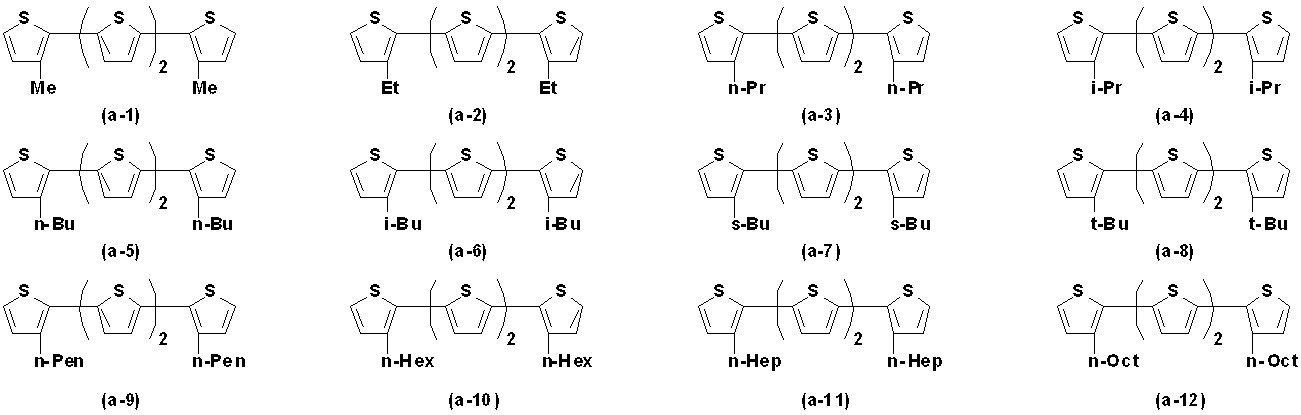
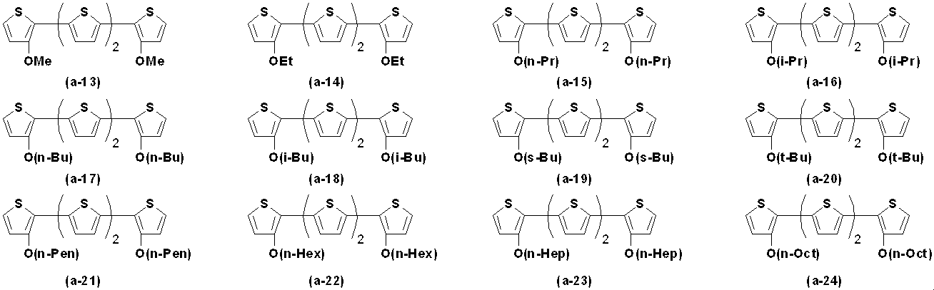
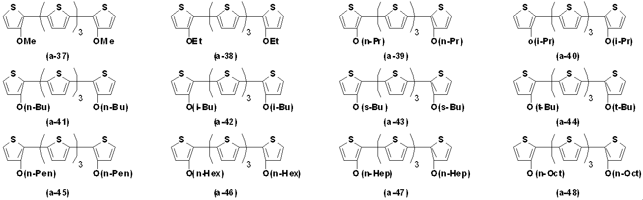
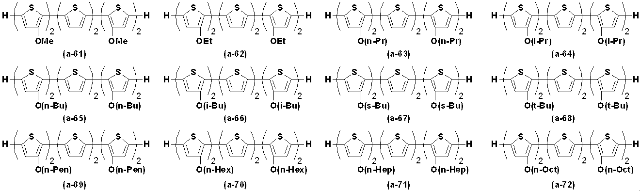
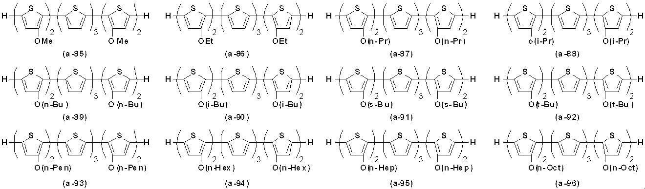
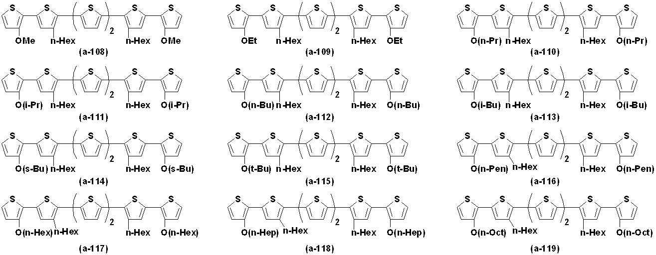
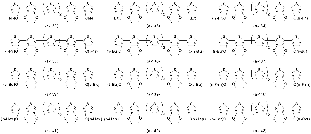
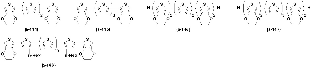
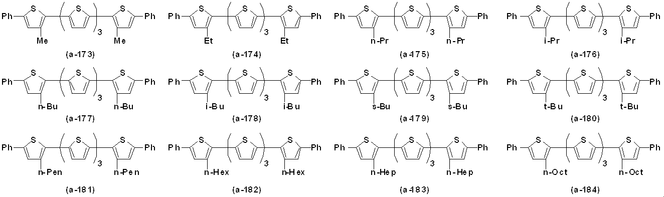
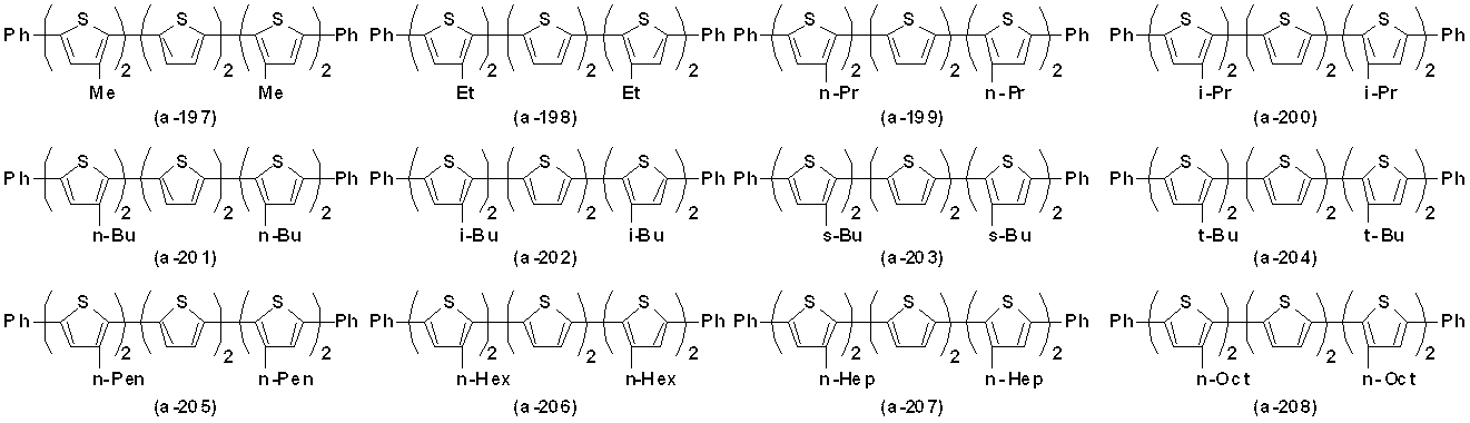
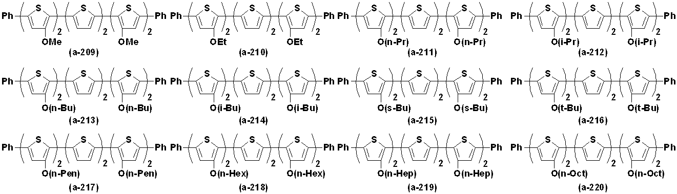
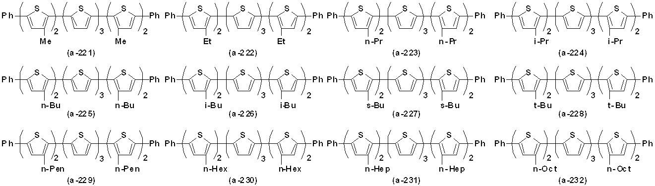
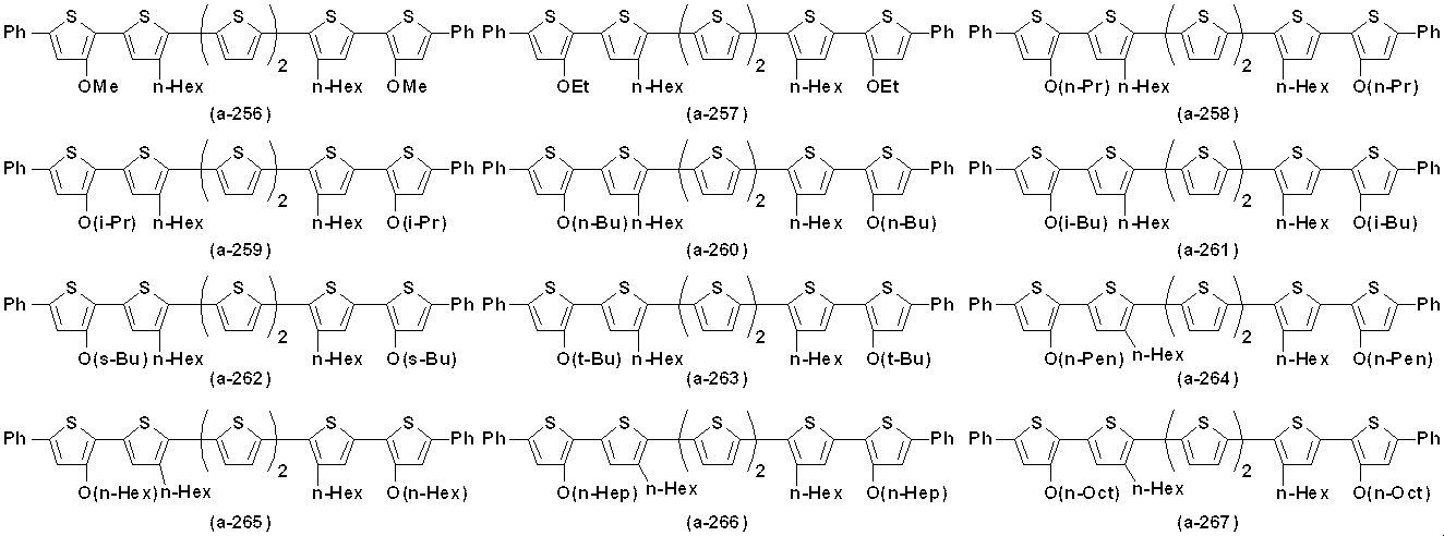
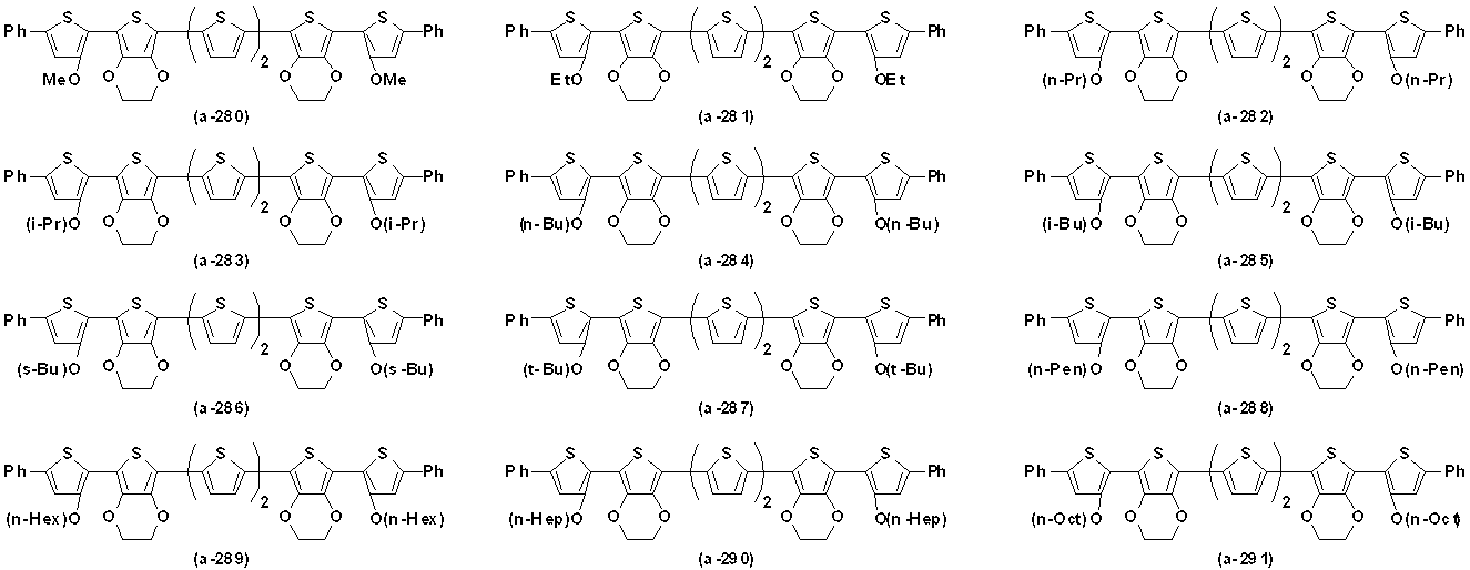
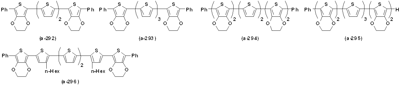
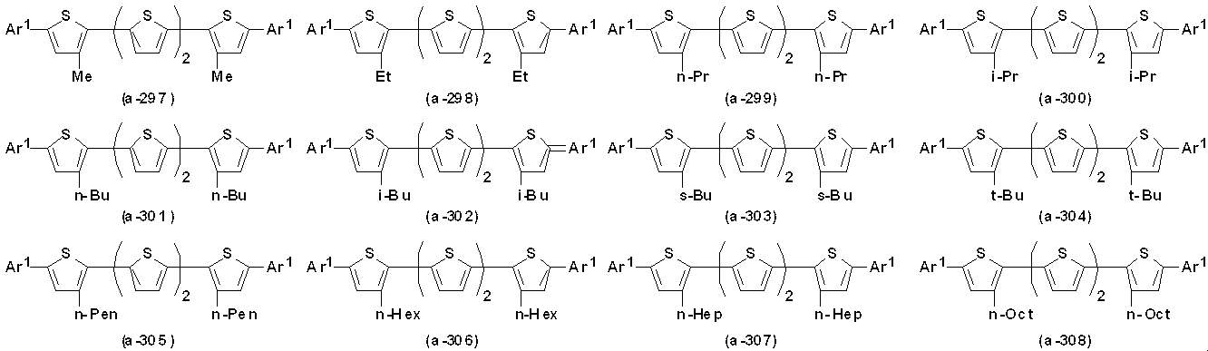
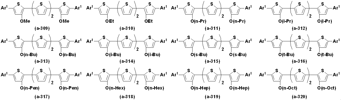
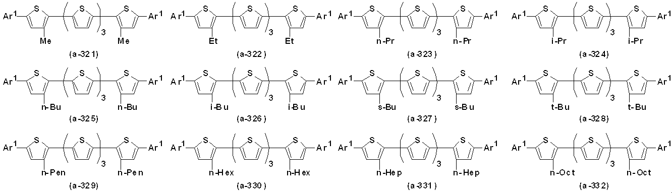
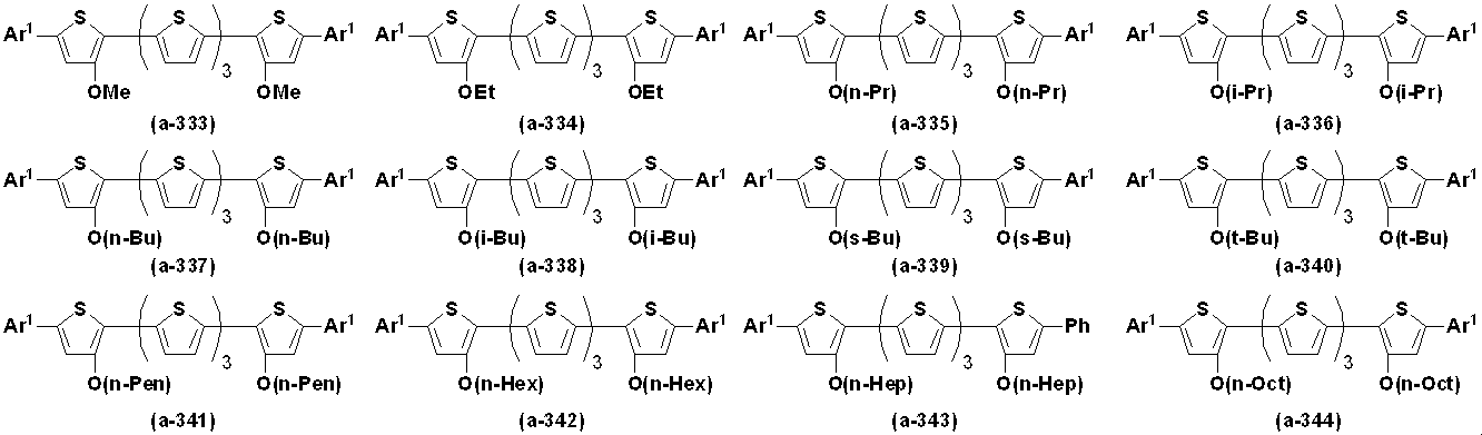
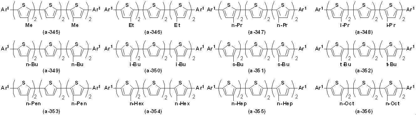
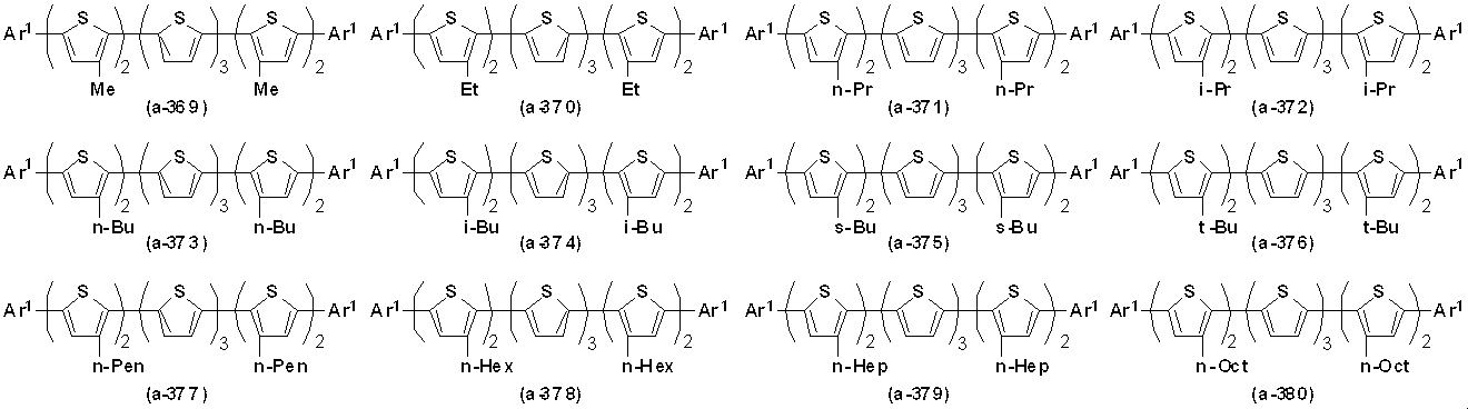
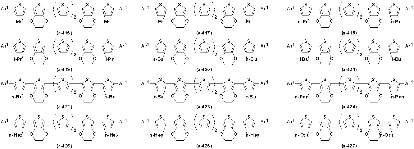
- oligothiophene derivative represented by Formula (1) is not necessarily limited to these.
- Me represents a methyl group
- Et represents an ethyl group
- n-Pr represents an n-propyl group
- i-Pr represents an i-propyl group
- n-Bu is an isobutyl group
- s-Bu is an s-butyl group
- t-Bu is a t-butyl group
- n-Pen is n-pentyl.
- N-Hex represents an n-hexyl group
- n-Hep represents an n-heptyl group
- n-Oct represents an n-octyl group
- Ph represents a phenyl group
- Ar 1 Represents a 4- (diphenylamino) phenyl group, respectively.
- the charge transporting varnish of the present invention contains a heteropolyacid, and therefore has only a high hole acceptability from a transparent electrode typified by indium tin oxide (ITO) and indium zinc oxide (IZO).
- ITO indium tin oxide
- IZO indium zinc oxide
- the heteropolyacid has a structure in which a hetero atom is located at the center of a molecule, which is typically represented by a Keggin type represented by the formula (D1) or a Dawson type chemical structure represented by the formula (D2), and vanadium ( V), molybdenum (Mo), tungsten (W), and other polyacids such as isopolyacids that are oxygen acids and oxygenates of different elements are condensed.
- the oxygen acid of such a different element mainly include silicon (Si), phosphorus (P), and arsenic (As) oxygen acids.
- heteropolyacid examples include phosphomolybdic acid, silicomolybdic acid, phosphotungstic acid, silicotungstic acid, and lintongue molybdic acid. These may be used alone or in combination of two or more. Good.
- the heteropolyacid used by this invention is available as a commercial item, and can also be synthesize
- the dopant material is composed of a single type of heteropolyacid alone
- the one type of heteropolyacid is preferably phosphotungstic acid or phosphomolybdic acid, and phosphotungstic acid is most suitable.
- the dopant substance is composed of two or more types of heteropolyacids
- one of the two or more types of heteropolyacids is preferably phosphotungstic acid or phosphomolybdic acid, and more preferably phosphotungstic acid.
- Heteropolyacids are available as commercial products in quantitative analysis such as elemental analysis, even if the number of elements is large or small from the structure represented by the general formula, or appropriate according to known synthesis methods. As long as it is synthesized, it can be used in the present invention. That is, for example, in general, phosphotungstic acid is represented by the chemical formula H 3 (PW 12 O 40 ) ⁇ nH 2 O, and phosphomolybdic acid is represented by the chemical formula H 3 (PMo 12 O 40 ) ⁇ nH 2 O, respectively.
- the mass of the heteropolyacid defined in the present invention is not the mass of pure phosphotungstic acid (phosphotungstic acid content) in the synthesized product or commercially available product, but a commercially available form and a known synthesis. In a form that can be isolated by the method, it means the total mass in a state containing hydration water and other impurities.
- the heteropolyacid contained in the charge transporting varnish of the present invention can be about 1.0 to 70.0 with respect to the charge transporting material 1 by mass ratio, but preferably 2.0 to 60.0. The degree is more preferably about 2.5 to 55.0.
- charge transporting varnish of the present invention other known charge transporting substances and dopant substances may be used in addition to the above-described oligothiophene derivatives and heteropolyacids.
- Examples of such other charge transporting substances include oligoaniline derivatives described in JP-A No. 2002-151272, oligoaniline compounds described in International Publication No. 2004/105446, and publications described in International Publication No. 2005/043962. Compounds having a 1,4-dithiine ring, oligoaniline compounds described in WO2008-032617, oligoaniline compounds described in WO2008 / 032616, aryldiamine compounds described in WO2013 / 042623, etc. Can be mentioned.
- aniline derivatives are preferable, and considering the solubility in organic solvents, the molecular weight is preferably 4000 or less, more preferably 3000 or less, and still more preferably 2000 or less.
- aniline derivatives that can be suitably used as other charge transporting materials include those represented by the formula (12).
- B 1 represents a single bond, —NH—, —CH 2 —, —S—, or —O—, and is preferably —NH— or a single bond.
- R 7 - R 12 are, independently of one another, a hydrogen atom, a halogen atom, Z 3 alkyl group which have 1 to 20 carbon atoms that may substituted, Z 3 - 2 carbon atoms which may be substituted with 20 alkenyl groups, Z 3-substituted 2 carbon atoms which may be 1-20 alkynyl group, Z 4-substituted-6 carbon atoms which may be 20 aryl group, a carbon may be substituted with Z 4 Represents a heteroaryl group of 2 to 20, a —OY 7 group, a —SY 8 group, —NHY 9 , —NY 10 Y 11 group, or —NHC (O) Y 12 group, and Y 7 to Y 12 represent each other independently, Z 3 substituted by optionally also be C 1 -C 20 alkyl group, an alkenyl group of Z 3 are optionally 2-20 carbon atoms substituted by, may be substituted with Z 3 carbon 2-20 alkynyl
- R 7 to R 10 are each a hydrogen atom, a halogen atom, an alkyl group having 1 to 20 carbon atoms which may be substituted with Z 3 , an aryl group having 6 to 20 carbon atoms which may be substituted with Z 4 , is preferably an alkyl group having carbon atoms which may 1 - 20 (-OY 7 groups Y 7 is an alkyl group of Z 3 is - 1 carbon atoms and optionally 20 substituted with) substituted with Z 3, hydrogen atom, a fluorine atom, an alkyl group which 1 carbon atoms which may be ⁇ 10 substituted by Z 3, an aryl group of Z 4 ⁇ carbon atoms 6 be replaced by 14, may be substituted with Z 3
- An alkyloxy group having 1 to 10 carbon atoms is more preferable, a hydrogen atom, a fluorine atom, an alkyl group having 1 to 6 carbon atoms which may be substituted with Z 3 , and an aryl group having 6 to 10 carbon
- R 11 and R 12 a hydrogen atom, a halogen atom, a dialkylamino group having 2 to 40 carbon atoms which may be substituted with Z 3 (Y 10 and Y 11 may be substituted with Z 3 ) -NY 10 Y 11 group which is an alkyl group having 1 to 20 carbon atoms, or a diarylamino group having 12 to 40 carbon atoms which may be substituted with Z 4 (Y 10 and Y 11 are substituted with Z 4) -NY 10 Y 11 group, which may be an aryl group having 6 to 20 carbon atoms, is preferable, a hydrogen atom, a fluorine atom, a dialkylamino group having 2 to 20 carbon atoms which may be substituted with Z 3 , or Z A diarylamino group having 12 to 20 carbon atoms which may be substituted with 4 is more preferred, a hydrogen atom, and a diarylamino group having 12 to 20 carbon atoms which may be substituted with Z
- p and q each independently represent an integer of 0 or more and satisfy 2 ⁇ p + q ⁇ 20, preferably 2 ⁇ p + q ⁇ 8, more preferably 2 ⁇ p + q ⁇ 6, More preferably, 2 ⁇ p + q ⁇ 4 is satisfied.
- the alkyl group, alkenyl group and alkynyl group of R 7 to R 12 and Y 7 to Y 12 are substituted with Z 3 which is an aryl group having 6 to 20 carbon atoms or a heteroaryl group having 2 to 20 carbon atoms.
- the aryl group and heteroaryl group of R 7 to R 12 and Y 7 to Y 12 may be an alkyl group having 1 to 20 carbon atoms, an alkenyl group having 2 to 20 carbon atoms, or an alkynyl group having 2 to 20 carbon atoms. May be substituted with Z 4 .
- Z 3 is preferably an aryl group having 6 to 20 carbon atoms, more preferably a phenyl group, and most preferably not present (that is, unsubstituted). It is.
- Z 4 is preferably an alkyl group having 1 to 20 carbon atoms, more preferably an alkyl group having 1 to 10 carbon atoms, still more preferably an alkyl group having 1 to 8 carbon atoms, and an alkyl group having 1 to 6 carbon atoms. Is more preferred and is optimally absent (ie, unsubstituted).
- aniline derivatives suitable as other charge transporting materials in the present invention will be given, but the invention is not limited thereto.
- dopant substances for example, benzenesulfonic acid, tosylic acid, p-styrenesulfonic acid, 2-naphthalenesulfonic acid, 4-hydroxybenzenesulfonic acid, 5-sulfosalicylic acid, p-dodecylbenzenesulfonic acid, dihexyl Benzenesulfonic acid, 2,5-dihexylbenzenesulfonic acid, dibutylnaphthalenesulfonic acid, 6,7-dibutyl-2-naphthalenesulfonic acid, dodecylnaphthalenesulfonic acid, 3-dodecyl-2-naphthalenesulfonic acid, hexylnaphthalenesulfonic acid, 4-hexyl-1-naphthalenesulfonic acid, octylnaphthalenesulfonic acid, 2-oc
- an aryl sulfonic acid compound is preferable, and considering the solubility in an organic solvent, the molecular weight is preferably 3000 or less, more preferably 2000 or less, and still more preferably 1000 or less.
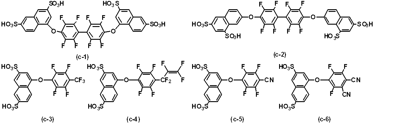
- examples of the aryl sulfonic acid compound that can be suitably used as other dopant substances include those represented by the formula (13) or (14).
- a 1 represents O or S, and O is preferable.
- a 2 represents a naphthalene ring or an anthracene ring, and a naphthalene ring is preferable.
- a 3 represents a divalent to tetravalent perfluorobiphenyl group, l represents the number of bonds between A 1 and A 3, is an integer satisfying 2 ⁇ l ⁇ 4, A 3 is a divalent par It is preferably a fluorobiphenyl group and 1 is 2.
- m represents the number of sulfonic acid groups bonded to A 2 and is an integer satisfying 1 ⁇ m ⁇ 4, but 2 is optimal.
- a 4 to A 8 each independently represent a hydrogen atom, a halogen atom, a cyano group, an alkyl group having 1 to 20 carbon atoms, a halogenated alkyl group having 1 to 20 carbon atoms, or the number of carbon atoms 2 to 20 halogenated alkenyl groups are represented, and at least three of A 4 to A 8 are halogen atoms.
- k represents the number of sulfonic acid groups bonded to the naphthalene ring and is an integer satisfying 1 ⁇ k ⁇ 4, preferably 2 to 4, and most preferably 2.
- halogenated alkyl group having 1 to 20 carbon atoms include those in which at least one hydrogen atom of the alkyl group having 1 to 20 carbon atoms is substituted with a halogen atom.
- Specific examples thereof include trifluoromethyl group, 2,2,2-trifluoroethyl group, 1,1,2,2,2-pentafluoroethyl group, 3,3,3-trifluoropropyl group, 2, 2,3,3,3-pentafluoropropyl group, 1,1,2,2,3,3,3-heptafluoropropyl group, 4,4,4-trifluorobutyl group, 3,3,4,4 , 4-pentafluorobutyl group, 2,2,3,3,4,4,4-heptafluorobutyl group, 1,1,2,2,3,3,4,4,4-nonafluorobutyl group, etc. Is mentioned.
- halogenated alkenyl group having 2 to 20 carbon atoms examples include those in which at least one hydrogen atom of the alkenyl group having 2 to 20 carbon atoms is substituted with a halogen atom.
- Specific examples thereof include a perfluorovinyl group, a perfluoropropenyl group (allyl group), and a perfluorobutenyl group.
- Other examples of the halogen atom and the alkyl group having 1 to 20 carbon atoms are the same as those described above, and the halogen atom is preferably a fluorine atom.
- a 4 to A 8 are a hydrogen atom, a halogen atom, a cyano group, an alkyl group having 1 to 10 carbon atoms, a halogenated alkyl group having 1 to 10 carbon atoms, or an alkenyl halide having 2 to 10 carbon atoms.
- at least three of A 4 to A 8 are preferably fluorine atoms, hydrogen atom, fluorine atom, cyano group, alkyl group having 1 to 5 carbon atoms, and 1 to 5 carbon atoms.
- it is a fluorinated alkyl group or a fluorinated alkenyl group having 2 to 5 carbon atoms, and at least three of A 4 to A 8 are fluorine atoms, a hydrogen atom, a fluorine atom, a cyano group, More preferably, it is a perfluoroalkyl group having 1 to 5 carbon atoms or a perfluoroalkenyl group having 1 to 5 carbon atoms, and A 4 , A 5 and A 8 are fluorine atoms.
- the perfluoroalkyl group is a group in which all hydrogen atoms of the alkyl group are substituted with fluorine atoms
- the perfluoroalkenyl group is a group in which all hydrogen atoms of the alkenyl group are substituted with fluorine atoms.
- a highly soluble solvent that can dissolve the charge transporting substance and the dopant substance satisfactorily can be used.
- highly soluble solvents include N, N-dimethylformamide, N, N-dimethylacetamide, N-methylpyrrolidone, 1,3-dimethyl-2-imidazolidinone, diethylene glycol monomethyl ether, propylene glycol monomethyl.
- An organic solvent such as ether can be used. These solvents can be used alone or in combination of two or more, and the amount used can be 5 to 100% by mass with respect to the total solvent used in the varnish.
- the charge transporting substance and the dopant substance are preferably either completely dissolved or uniformly dispersed in the solvent, and more preferably completely dissolved.
- the varnish has a viscosity of 10 to 200 mPa ⁇ s, particularly 35 to 150 mPa ⁇ s at 25 ° C., and a boiling point of 50 to 300 ° C., particularly 150 to 250 ° C. at normal pressure (atmospheric pressure).
- a viscosity 10 to 200 mPa ⁇ s, particularly 35 to 150 mPa ⁇ s at 25 ° C., and a boiling point of 50 to 300 ° C., particularly 150 to 250 ° C. at normal pressure (atmospheric pressure).
- the high-viscosity organic solvent is not particularly limited, and examples thereof include cyclohexanol, ethylene glycol, ethylene glycol diglycidyl ether, 1,3-octylene glycol, diethylene glycol, dipropylene glycol, triethylene glycol, and tripropylene glycol. 1,3-butanediol, 2,3-butanediol, 1,4-butanediol, propylene glycol, hexylene glycol and the like. These solvents may be used alone or in combination of two or more.
- the addition ratio of the high-viscosity organic solvent to the entire solvent used in the varnish of the present invention is preferably in the range where no solid precipitates, and the addition ratio is preferably 5 to 80% by mass as long as no solid precipitates.
- solvents are used in an amount of 1 to 90% by mass, preferably It is also possible to mix at a ratio of 1 to 50% by mass.
- solvents examples include ethylene glycol monobutyl ether, diethylene glycol diethyl ether, diethylene glycol dimethyl ether, diethylene glycol monoethyl ether acetate, diethylene glycol monobutyl ether acetate, dipropylene glycol monomethyl ether, propylene glycol monomethyl ether acetate, diethylene glycol monoethyl ether, diethylene glycol Examples include, but are not limited to, acetone alcohol, ⁇ -butyrolactone, ethyl lactate, n-hexyl acetate, and the like. These solvents can be used alone or in combination of two or more.
- the viscosity of the varnish of the present invention is appropriately set according to the thickness of the thin film to be produced and the solid content concentration, but is usually 1 to 50 mPa ⁇ s at 25 ° C.
- the solid content concentration of the charge transporting varnish in the present invention is appropriately set in consideration of the viscosity and surface tension of the varnish, the thickness of the thin film to be produced, etc. In consideration of improving the coatability of the varnish, it is preferably 0.5 to 5.0% by mass, more preferably 1.0 to 3.0% by mass.
- a charge transporting thin film can be formed on a base material by applying the charge transporting varnish described above onto the base material and baking it.
- the method for applying the varnish is not particularly limited, and examples thereof include a dipping method, a spin coating method, a transfer printing method, a roll coating method, a brush coating, an ink jet method, and a spray method. It is preferable to adjust the viscosity and surface tension.
- the firing atmosphere is not particularly limited, and a thin film having a uniform film formation surface and a high charge transport property in not only an air atmosphere but also an inert gas such as nitrogen or a vacuum. It is possible to obtain.
- the firing temperature is appropriately set within a range of about 100 to 260 ° C. in consideration of the use of the obtained thin film, the degree of charge transportability imparted to the obtained thin film, and the like.
- the temperature is preferably about 140 to 250 ° C, more preferably about 145 to 240 ° C.
- a temperature change of two or more steps may be applied for the purpose of developing a higher uniform film forming property or causing the reaction to proceed on the substrate. What is necessary is just to perform using suitable apparatuses, such as oven.
- the thickness of the charge transporting thin film is not particularly limited, but is preferably 5 to 200 nm when used as a hole injection layer in an organic EL device.
- a method of changing the film thickness there are methods such as changing the solid content concentration in the varnish and changing the amount of the solution on the substrate during coating.
- Examples of materials used and methods for producing an OLED element using the charge transporting varnish of the present invention include the following, but are not limited thereto.
- the electrode substrate to be used is preferably cleaned in advance by liquid cleaning with a detergent, alcohol, pure water or the like.
- the anode substrate is subjected to surface treatment such as UV ozone treatment or oxygen-plasma treatment immediately before use. It is preferable.
- the anode material is mainly composed of an organic material, the surface treatment may not be performed.
- the example of the manufacturing method of the OLED element which has a positive hole injection layer which consists of a thin film obtained from the charge transportable varnish of this invention is as follows.
- the charge transporting varnish of the present invention is applied onto the anode substrate and baked to produce a hole injection layer on the electrode.
- This is introduced into a vacuum deposition apparatus, and a hole transport layer, a light emitting layer, an electron transport layer / hole block layer, an electron injection layer, and a cathode metal are sequentially deposited to form an OLED element.
- an electron blocking layer may be provided between the light emitting layer and the hole transport layer.
- anode material examples include transparent electrodes typified by indium tin oxide (ITO) and indium zinc oxide (IZO), metal anodes typified by aluminum, alloys thereof, and the like. What performed the chemical conversion process is preferable. Polythiophene derivatives and polyaniline derivatives having high charge transporting properties can also be used. Examples of other metals constituting the metal anode include scandium, titanium, vanadium, chromium, manganese, iron, cobalt, nickel, copper, zinc, gallium, yttrium, zirconium, niobium, molybdenum, ruthenium, rhodium, and palladium.
- Cadmium indium, scandium, lanthanum, cerium, praseodymium, neodymium, promethium, samarium, europium, gadolinium, terbium, dysprosium, holmium, erbium, thulium, ytterbium, hafnium, thallium, tungsten, rhenium, osmium, iridium, platinum, gold , Titanium, lead, bismuth and alloys thereof.
- Materials for forming the hole transport layer include (triphenylamine) dimer derivative, [(triphenylamine) dimer] spirodimer, N, N′-bis (naphthalen-1-yl) -N, N′-bis (Phenyl) -benzidine ( ⁇ -NPD), N, N′-bis (naphthalen-2-yl) -N, N′-bis (phenyl) -benzidine, N, N′-bis (3-methylphenyl)- N, N′-bis (phenyl) -benzidine, N, N′-bis (3-methylphenyl) -N, N′-bis (phenyl) -9,9-spirobifluorene, N, N′-bis ( Naphthalen-1-yl) -N, N′-bis (phenyl) -9,9-spirobifluorene, N, N′-bis (3-methylphenyl) -N, N′-bis (phenyl) -9,9-spir
- Materials for forming the light emitting layer include tris (8-quinolinolato) aluminum (III) (Alq 3 ), bis (8-quinolinolato) zinc (II) (Znq 2 ), bis (2-methyl-8-quinolinolato) ( p-phenylphenolate) aluminum (III) (BAlq), 4,4′-bis (2,2-diphenylvinyl) biphenyl, 9,10-di (naphthalen-2-yl) anthracene, 2-t-butyl- 9,10-di (naphthalen-2-yl) anthracene, 2,7-bis [9,9-di (4-methylphenyl) -fluoren-2-yl] -9,9-di (4-methylphenyl) Fluorene, 2-methyl-9,10-bis (naphthalen-2-yl) anthracene, 2- (9,9-spirobifluoren-2-yl) -9,9-spirobifluore 2,
- luminescent dopants examples include 3- (2-benzothiazolyl) -7- (diethylamino) coumarin, 2,3,6,7-tetrahydro-1,1,7,7-tetramethyl-1H, 5H, 11H-10-.
- Materials for forming the electron transport layer / hole block layer include 8-hydroxyquinolinolate-lithium, 2,2 ′, 2 ′′-(1,3,5-benztolyl) -tris (1-phenyl-1- H-benzimidazole), 2- (4-biphenyl) 5- (4-t-butylphenyl) -1,3,4-oxadiazole, 2,9-dimethyl-4,7-diphenyl-1,10- Phenanthroline, 4,7-diphenyl-1,10-phenanthroline, bis (2-methyl-8-quinolinolate) -4- (phenylphenolato) aluminum, 1,3-bis [2- (2,2′-bipyridine- 6-yl) -1,3,4-oxadiazo-5-yl] benzene, 6,6′-bis [5- (biphenyl-4-yl) -1,3,4-oxadiazo-2-yl] -2 , 2'- Pyridine, 3- (4-bi
- Materials for forming the electron injection layer include lithium oxide (Li 2 O), magnesium oxide (MgO), alumina (Al 2 O 3 ), lithium fluoride (LiF), sodium fluoride (NaF), magnesium fluoride ( MgF 2 ), cesium fluoride (CsF), strontium fluoride (SrF 2 ), molybdenum trioxide (MoO 3 ), aluminum, Li (acac), lithium acetate, lithium benzoate, and the like.
- Examples of the cathode material include aluminum, magnesium-silver alloy, aluminum-lithium alloy, lithium, sodium, potassium, cesium and the like.
- Examples of the material for forming the electron blocking layer include tris (phenylpyrazole) iridium.
- the manufacturing method of the PLED element using the charge transportable varnish of this invention is not specifically limited, The following methods are mentioned.
- the hole transport polymer layer and the light emitting polymer layer are sequentially formed.
- a PLED element having a charge transporting thin film formed by the charge transporting varnish of the invention can be produced.
- the charge transporting varnish of the present invention is applied on the anode substrate to prepare a hole injection layer by the above method, and a hole transporting polymer layer and a light emitting polymer layer are sequentially formed thereon. Then, a cathode electrode is vapor-deposited to obtain a PLED element.
- the hole transporting polymer layer and the light emitting polymer layer can be formed by adding a solvent to a hole transporting polymer material or a light emitting polymer material, or a material obtained by adding a dopant substance to the hole transporting polymer material. And a method of forming a film by uniformly dispersing and coating the film on a hole injection layer or a hole transporting polymer layer and then firing the respective layers.
- Examples of the light-emitting polymer material include polyfluorene derivatives such as poly (9,9-dialkylfluorene) (PDAF), poly (2-methoxy-5- (2′-ethylhexoxy) -1,4-phenylenevinylene) (MEH). And polyphenylene vinylene derivatives such as -PPV), polythiophene derivatives such as poly (3-alkylthiophene) (PAT), and polyvinylcarbazole (PVCz).
- polyfluorene derivatives such as poly (9,9-dialkylfluorene) (PDAF), poly (2-methoxy-5- (2′-ethylhexoxy) -1,4-phenylenevinylene) (MEH).
- polyphenylene vinylene derivatives such as -PPV
- polythiophene derivatives such as poly (3-alkylthiophene) (PAT)
- PVCz polyvinylcarbazole
- Examples of the solvent include toluene, xylene, chloroform, and the like.
- Examples of the dissolution or uniform dispersion method include methods such as stirring, heating and stirring, and ultrasonic dispersion.
- the application method is not particularly limited, and examples thereof include an inkjet method, a spray method, a dipping method, a spin coating method, a transfer printing method, a roll coating method, and a brush coating method.
- the application is preferably performed under an inert gas such as nitrogen or argon.
- Examples of the firing method include a method of heating in an oven or a hot plate under an inert gas or in a vacuum.
- Example 1-2 to 1-5 The amount of TP1 used and the amount of phosphotungstic acid used were 0.093 g and 0.278 g (Example 1-2), 0.074 g and 0.297 g (Example 1-3), 0.062 g and 0, respectively.
- a charge transporting varnish was prepared in the same manner as in Example 1-1 except that 309 g (Example 1-4), 0.053 g, and 0.318 g (Example 1-5) were used.
- Example 1-6 A charge transporting varnish was prepared in the same manner as in Example 1-1 except that 0.062 g of TP3 was used instead of 0.124 g of TP1, and the amount of phosphotungstic acid was 0.309 g.
- Example 1-7 to 1-8 Except that the amount of TP3 and the amount of phosphotungstic acid used were 0.034 g and 0.337 g (Example 1-7), 0.018 g and 0.353 g (Example 1-8), respectively.
- a charge transporting varnish was prepared in the same manner as in 1-6.
- Example 1-9 0.116 g of TP5 and 0.348 g of phosphotungstic acid were dissolved in 10.5 g of 1,3-dimethyl-2-imidazolidinone under a nitrogen atmosphere. To the resulting solution, 3 g of 2,3-butanediol and 1.5 g of propylene glycol monomethyl ether were sequentially added and stirred to prepare a charge transporting varnish.
- the thin film produced using the charge transporting varnish of the present invention was found to have a high transmittance of 95% or more in the visible region.
- Example 3-1 Manufacture and characteristic evaluation of organic EL device
- the varnish obtained in Example 1-1 was applied to an ITO substrate using a spin coater, then dried at 50 ° C. for 5 minutes, and further baked at 230 ° C. for 10 minutes in an air atmosphere. A uniform thin film of 30 nm was formed.
- As the ITO substrate a glass substrate of 25 mm ⁇ 25 mm ⁇ 0.7 t in which indium tin oxide (ITO) is patterned on the surface with a film thickness of 150 nm is used, and an O 2 plasma cleaning apparatus (150 W, 30 seconds) before use. To remove impurities on the surface.
- ITO indium tin oxide
- a thin film of ⁇ -NPD, Alq 3 , lithium fluoride, and aluminum is sequentially laminated on the ITO substrate on which the thin film is formed using a vapor deposition apparatus (degree of vacuum: 1.0 ⁇ 10 ⁇ 5 Pa). An element was obtained. At this time, the deposition rate was 0.2 nm / second for ⁇ -NPD, Alq 3 and aluminum, and 0.02 nm / second for lithium fluoride, and the film thicknesses were 30 nm, 40 nm, and 0.2 nm, respectively. The thickness was 5 nm and 120 nm.
- the characteristic was evaluated. Sealing was performed according to the following procedure. In a nitrogen atmosphere with an oxygen concentration of 2 ppm or less and a dew point of -85 ° C or less, the organic EL element is placed between the sealing substrates, and the sealing substrate is bonded with an adhesive (XNR5516Z-B1 manufactured by Nagase ChemteX Corporation). It was. At this time, a water catching agent (manufactured by Dynic Co., Ltd., HD-071010W-40) was placed in the sealing substrate together with the organic EL element. The bonded sealing substrate was irradiated with UV light (wavelength: 365 nm, irradiation amount: 6000 mJ / cm 2 ), and then annealed at 80 ° C. for 1 hour to cure the adhesive.
- UV light wavelength: 365 nm, irradiation amount: 6000 mJ / cm 2
- Examples 3-2 to 3-9 An organic EL device was prepared in the same manner as in Example 3-1, except that the varnishes obtained in Examples 1-2 to 1-9 were used instead of the varnish obtained in Example 1-1. Produced.
- Example 1 A device was produced in the same manner as in Example 3-1, except that PEDOT / PSS (AI4083 manufactured by HC Starck) was used instead of the varnish obtained in Example 1-1.
- PEDOT / PSS AI4083 manufactured by HC Starck
- the current density and luminance at a driving voltage of 5 V of the manufactured element were measured.
- the luminance half-life (LT50) initial luminance 5000 cd / m 2 , the same applies hereinafter
- the luminance is the initial luminance.
- the durability test was performed by measuring the time (LT80) of 80%. The results are shown in Table 2. The expected half-life of the element of Example 3-9 at the time of LT80 is also shown.
- the organic EL devices having the hole injection layer obtained from the varnish of the present invention have not only excellent luminance characteristics but also general It can be seen that the durability is far superior to that in the case of using a polythiophene (PEDOT / PSS) hole injection layer which is a charge transporting material (Comparative Example 1).
- PEDOT / PSS polythiophene
Landscapes
- Chemical & Material Sciences (AREA)
- Organic Chemistry (AREA)
- Physics & Mathematics (AREA)
- Spectroscopy & Molecular Physics (AREA)
- Electroluminescent Light Sources (AREA)
- Engineering & Computer Science (AREA)
- Life Sciences & Earth Sciences (AREA)
- Materials Engineering (AREA)
- Wood Science & Technology (AREA)
- Chemical Kinetics & Catalysis (AREA)
- Heterocyclic Compounds Containing Sulfur Atoms (AREA)
- Heterocyclic Carbon Compounds Containing A Hetero Ring Having Oxygen Or Sulfur (AREA)
- Nitrogen And Oxygen Or Sulfur-Condensed Heterocyclic Ring Systems (AREA)
Abstract
Description
この電荷輸送性薄膜の着色は、有機EL素子の色純度および色再現性を低下させることが知られている。
しかも、このような着色は、3色発光法、白色法および色変換法などの有機ELディスプレイにおける種々のフルカラー化技術において問題になり、有機EL素子を安定に生産する際の著しい障害になる。
このような事情から、有機EL素子の電荷輸送性薄膜は、可視領域での透過率が高く、高透明性を有することが望まれており、本発明者らは、それに鑑み、各種ウェットプロセスに適用可能であるとともに、有機EL素子の正孔注入層に適用した場合に優れたEL素子特性を実現できる透明性に優れた薄膜を与える電荷輸送性材料を開発してきている(特許文献1参照)。
なお、特許文献2には、オリゴチオフェン誘導体およびヘテロポリ酸を用いたワニスは、具体的に開示されていない。
1. 式(1)で表されるオリゴチオフェン誘導体からなる電荷輸送性物質と、ヘテロポリ酸からなるドーパント物質と、有機溶媒とを含むことを特徴とする電荷輸送性ワニス、

2. 前記オリゴチオフェン誘導体が、式(2)で表される1の電荷輸送性ワニス、
3. 1または2の電荷輸送性ワニスを用いて作製される電荷輸送性薄膜、
4. 3の電荷輸送性薄膜を有する電子デバイス、
5. 3の電荷輸送性薄膜を有する有機エレクトロルミネッセンス素子、
6. 前記電荷輸送性薄膜が、正孔注入層または正孔輸送層である5の有機エレクトロルミネッセンス素子、
7. 1または2の電荷輸送性ワニスを基材上に塗布して焼成することを特徴とする電荷輸送性薄膜の製造方法、
8. 3の電荷輸送性薄膜を用いることを特徴とする有機エレクトロルミネッセンス素子の製造方法
を提供する。
本発明の電荷輸送性ワニスを用いることで、高い透明性および導電性を備えた電荷輸送性薄膜が得られ、この薄膜を、特に有機EL素子の正孔注入層に適用することで、高い発光効率を有し、かつ、耐久性に優れた有機EL素子を得ることができる。
また、本発明の電荷輸送性ワニスは、スピンコート法やスリットコート法など、大面積に成膜可能な各種ウェットプロセスを用いた場合でも電荷輸送性に優れた薄膜を再現性よく製造できるため、近年の有機EL素子の分野における進展にも十分対応できる。
さらに、本発明の電荷輸送性ワニスから得られる薄膜は、帯電防止膜や有機薄膜太陽電池の陽極バッファ層等としても使用できる。
本発明に係る電荷輸送性ワニスは、式(1)で表されるオリゴチオフェン誘導体からなる電荷輸送性物質と、ヘテロポリ酸からなるドーパント物質と、有機溶媒とを含む。
ここで、電荷輸送性とは、導電性と同義であり、正孔輸送性と同義である。電荷輸送性物質は、それ自体に電荷輸送性があるものでもよく、電子受容性物質と共に用いた際に電荷輸送性があるものでもよい。電荷輸送性ワニスは、それ自体に電荷輸送性があるものでもよく、それにより得られる固形膜が電荷輸送性を有するものでもよい。

また、オリゴチオフェン誘導体の有機溶媒への溶解性を向上させる観点から、n1~n3は、好ましくはn1+n2+n3≦8、より好ましくはn1+n2+n3≦7、より一層好ましくはn1+n2+n3≦6、さらに好ましくはn1+n2+n3≦5を満たす。
すなわち、本発明で用いるオリゴチオフェン誘導体は、具体的には、例えば、下記スキーム1および2によって、合成することができ、また、特に、両末端に、アルキル基、アルケニル基、アルキニル基、アリール基またはヘテロアリール基を有するオリゴチオフェン誘導体(式(1’))は、下記スキーム3によって、合成することもできる。
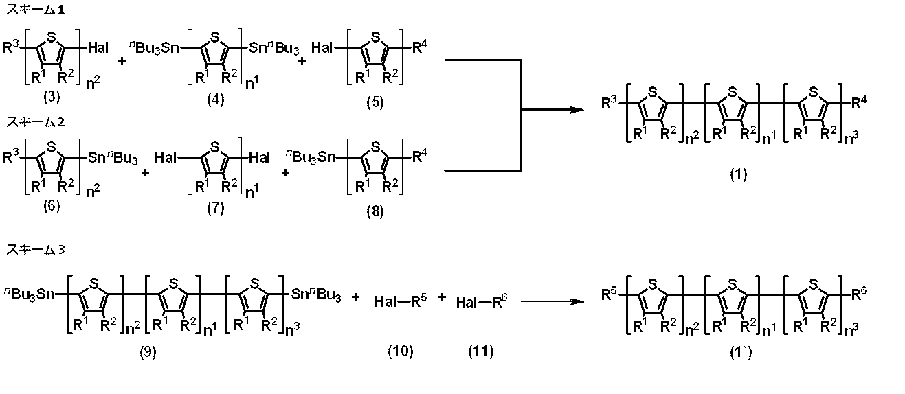
擬ハロゲン基としては、メタンスルホニルオキシ基、トリフルオロメタンスルホニルオキシ基、ノナフルオロブタンスルホニルオキシ基等の(フルオロ)アルキルスルホニルオキシ基;ベンゼンスルホニルオキシ基、トルエンスルホニルオキシ基等の芳香族スルホニルオキシ基などが挙げられる。
スキーム2において、式(6)~(8)で表されるチオフェン誘導体の仕込みは、通常、式(7)で表されるチオフェン誘導体に対し、式(6)で表されるチオフェン誘導体、式(8)で表されるチオフェン誘導体それぞれ0.5~1.5当量程度であるが、0.9~1.3当量程度が好適である。
スキーム3において、式(9)で表されるチオフェン誘導体および式(10)~(11)で表される化合物の仕込みは、通常、式(9)で表されるチオフェン誘導体に対し、式(10)で表される化合物、式(11)で表される化合物それぞれ0.5~1.5当量程度であるが、0.9~1.3当量程度が好適である。
また、配位子が同時に使用される場合の配位子の使用量は、使用する金属錯体に対し、0.1~5当量程度でよいが、1~4当量程度が好適である。
反応終了後は、常法に従って後処理をして、式(1)または(1’)で表されるオリゴチオフェン誘導体を得ることができる。
一方、式(3)、(5)、(7)、(10)および(11)で表される化合物は、市販品を用いることもできるし、一般的に用いられる手法に従い、各化合物に対応する構造を有する、チオフェン、アルカン、アルケン、アルキン、アレーンまたはチオフェン以外のヘテロアレーンをハロゲン化または擬ハロゲン化することで得ることができる。
なお、式中、「Me」はメチル基を、「Et」はエチル基を、「n-Pr」はn-プロピル基を、「i-Pr」はi-プロピル基を、「n-Bu」はn-ブチル基を、「i-Bu」はイソブチル基を、「s-Bu」はs-ブチル基を、「t-Bu」はt-ブチル基を、「n-Pen」はn-ペンチル基を、「n-Hex」はn-ヘキシル基を、「n-Hep」はn-ヘプチル基を、「n-Oct」はn-オクチル基を、「Ph」はフェニル基を、「Ar1」は4-(ジフェニルアミノ)フェニル基を、それぞれ示す。
















すなわち、例えば、一般的には、リンタングステン酸は化学式H3(PW12O40)・nH2Oで、リンモリブデン酸は化学式H3(PMo12O40)・nH2Oでそれぞれ示されるが、定量分析において、この式中のP(リン)、O(酸素)またはW(タングステン)もしくはMo(モリブデン)の数が多く、または少ないものであっても、それが市販品として入手したもの、あるいは、公知の合成方法に従い適切に合成したものである限り、本発明において用いることができる。この場合、本発明に規定されるヘテロポリ酸の質量とは、合成物や市販品中における純粋なリンタングステン酸の質量(リンタングステン酸含量)ではなく、市販品として入手可能な形態および公知の合成法にて単離可能な形態において、水和水やその他の不純物等を含んだ状態での全質量を意味する。
その他の電荷輸送性物として好適に用い得るアニリン誘導体としては、例えば、式(12)で表されるものが挙げられる。


とりわけ、その他のドーパント物質としては、アリールスルホン酸化合物が好ましく、有機溶媒への溶解性を考慮すると、その分子量は、好ましく3000以下、より好ましくは2000以下、より一層好ましくは1000以下である。
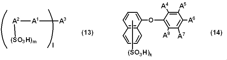
A2は、ナフタレン環またはアントラセン環を表すが、ナフタレン環が好ましい。
A3は、2~4価のパーフルオロビフェニル基を表し、lは、A1とA3との結合数を示し、2≦l≦4を満たす整数であるが、A3が2価のパーフルオロビフェニル基であり、かつ、lが2であることが好ましい。
mは、A2に結合するスルホン酸基数を表し、1≦m≦4を満たす整数であるが、2が最適である。
kは、ナフタレン環に結合するスルホン酸基数を表し、1≦k≦4を満たす整数であるが、2~4が好ましく、2が最適である。
その他、ハロゲン原子、炭素数1~20のアルキル基の例としては上記と同様のものが挙げられるが、ハロゲン原子としては、フッ素原子が好ましい。
なお、パーフルオロアルキル基とは、アルキル基の水素原子全てがフッ素原子に置換された基であり、パーフルオロアルケニル基とは、アルケニル基の水素原子全てがフッ素原子に置換された基である。
このような高溶解性溶媒としては、例えば、N,N-ジメチルホルムアミド、N,N-ジメチルアセトアミド、N-メチルピロリドン、1,3-ジメチル-2-イミダゾリジノン、ジエチレングリコールモノメチルエーテル、プロピレングリコールモノメチルエーテル等の有機溶媒を用いることができる。これらの溶媒は1種単独で、または2種以上混合して用いることができ、その使用量は、ワニスに使用する溶媒全体に対して5~100質量%とすることができる。
なお、電荷輸送性物質およびドーパント物質は、いずれも上記溶媒に完全に溶解しているか、均一に分散している状態となっていることが好ましく、完全に溶解していることがより好ましい。
高粘度有機溶媒としては、特に限定されるものではなく、例えば、シクロヘキサノール、エチレングリコール、エチレングリコールジクリシジルエーテル、1,3-オクチレングリコール、ジエチレングリコール、ジプロピレングリコール、トリエチレングリコール、トリプロピレングリコール、1,3-ブタンジオール、2,3-ブタンジオール、1,4-ブタンジオール、プロピレングリコール、へキシレングリコール等が挙げられる。これらの溶媒は単独で用いてもよく、2種以上混合して用いてもよい。
本発明のワニスに用いられる溶媒全体に対する高粘度有機溶媒の添加割合は、固体が析出しない範囲内であることが好ましく、固体が析出しない限りにおいて、添加割合は、5~80質量%が好ましい。
このような溶媒としては、例えば、エチレングリコールモノブチルエーテル、ジエチレングリコールジエチルエーテル、ジエチレングリコールジメチルエーテル、ジエチレングリコールモノエチルエーテルアセテート、ジエチレングリコールモノブチルエーテルアセテート、ジプロピレングリコールモノメチルエーテル、プロピレングリコールモノメチルエーテルアセテート、ジエチレングリコールモノエチルエーテル、ジアセトンアルコール、γ-ブチロラクトン、エチルラクテート、n-ヘキシルアセテート等が挙げられるが、これらに限定されるものではない。これらの溶媒は1種単独で、または2種以上混合して用いることができる。
また、本発明における電荷輸送性ワニスの固形分濃度は、ワニスの粘度および表面張力等や、作製する薄膜の厚み等を勘案して適宜設定されるものではあるが、通常、0.1~10.0質量%程度であり、ワニスの塗布性を向上させることを考慮すると、好ましくは0.5~5.0質量%、より好ましくは1.0~3.0質量%である。
ワニスの塗布方法としては、特に限定されるものではなく、ディップ法、スピンコート法、転写印刷法、ロールコート法、刷毛塗り、インクジェット法、スプレー法等が挙げられ、塗布方法に応じてワニスの粘度および表面張力を調節することが好ましい。
なお、焼成の際、より高い均一成膜性を発現させたり、基材上で反応を進行させたりする目的で、2段階以上の温度変化をつけてもよく、加熱は、例えば、ホットプレートやオーブン等、適当な機器を用いて行えばよい。
使用する電極基板は、洗剤、アルコール、純水等による液体洗浄を予め行って浄化しておくことが好ましく、例えば、陽極基板では使用直前にUVオゾン処理、酸素-プラズマ処理等の表面処理を行うことが好ましい。ただし陽極材料が有機物を主成分とする場合、表面処理を行わなくともよい。
上記の方法により、陽極基板上に本発明の電荷輸送性ワニスを塗布して焼成し、電極上に正孔注入層を作製する。これを真空蒸着装置内に導入し、正孔輸送層、発光層、電子輸送層/ホールブロック層、電子注入層、陰極金属を順次蒸着してOLED素子とする。なお、必要に応じて、発光層と正孔輸送層との間に電子ブロック層を設けてよい。
なお、金属陽極を構成するその他の金属としては、例えば、スカンジウム、チタン、バナジウム、クロム、マンガン、鉄、コバルト、ニッケル、銅、亜鉛、ガリウム、イットリウム、ジルコニウム、ニオブ、モリブデン、ルテニウム、ロジウム、パラジウム、カドニウム、インジウム、スカンジウム、ランタン、セリウム、プラセオジム、ネオジム、プロメチウム、サマリウム、ユウロピウム、ガドリニウム、テルビウム、ジスプロシウム、ホルミウム、エルビウム、ツリウム、イッテルビウム、ハフニウム、タリウム、タングステン、レニウム、オスミウム、イリジウム、プラチナ、金、チタン、鉛、ビスマスやそれらの合金等が挙げられる。
陰極材料としては、アルミニウム、マグネシウム-銀合金、アルミニウム-リチウム合金、リチウム、ナトリウム、カリウム、セシウム等が挙げられる。
電子ブロック層を形成する材料としては、トリス(フェニルピラゾール)イリジウム等が挙げられる。
上記OLED素子作製において、正孔輸送層、発光層、電子輸送層、電子注入層の真空蒸着操作を行う代わりに、正孔輸送性高分子層、発光性高分子層を順次形成することによって本発明の電荷輸送性ワニスによって形成される電荷輸送性薄膜を有するPLED素子を作製することができる。
具体的には、陽極基板上に本発明の電荷輸送性ワニスを塗布して上記の方法により正孔注入層を作製し、その上に正孔輸送性高分子層、発光性高分子層を順次形成し、さらに陰極電極を蒸着してPLED素子とする。
正孔輸送性高分子層および発光性高分子層の形成法としては、正孔輸送性高分子材料もしくは発光性高分子材料、またはこれらにドーパント物質を加えた材料に溶媒を加えて溶解するか、均一に分散し、正孔注入層または正孔輸送性高分子層の上に塗布した後、それぞれ焼成することで成膜する方法が挙げられる。
塗布方法としては、特に限定されるものではなく、インクジェット法、スプレー法、ディップ法、スピンコート法、転写印刷法、ロールコート法、刷毛塗り等が挙げられる。なお、塗布は、窒素、アルゴン等の不活性ガス下で行うことが好ましい。
焼成する方法としては、不活性ガス下または真空中、オーブンまたはホットプレートで加熱する方法が挙げられる。
(1)基板洗浄:長州産業(株)製 基板洗浄装置(減圧プラズマ方式)
(2)ワニスの塗布:ミカサ(株)製 スピンコーターMS-A100
(3)膜厚測定:(株)小坂研究所製 微細形状測定機サーフコーダET-4000
(4)透過率測定:(株)島津製作所社製 可視紫外線吸収スペクトル測定装置UV-3100PC
(5)EL素子の作製:長州産業(株)製 多機能蒸着装置システムC-E2L1G1-N
(6)EL素子の輝度等の測定:(有)テック・ワールド製 I-V-L測定システム
(7)EL素子の寿命測定(半減期等の測定および予想半減期の見積):(株)イーエッチシー製 有機EL輝度寿命評価システムPEL-105S
[合成例1]
実施例で使用する式(a-58)で表されるオリゴチオフェン誘導体2(以下、TP2ともいう。)を以下の方法により合成した。
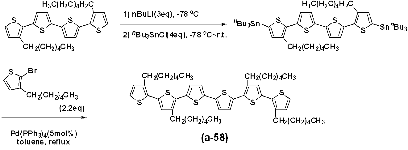
撹拌後、イオン交換水およびノルマルヘキサンを加え分液し、得られた有機層を更にイオン交換水で2回洗浄した後、硫酸ナトリウムを用いて乾燥した。
そして、溶媒を留去して3,3’’’-ジヘキシル-[2,2’:5’,2’’:5’’,2’’’-クウォーターチオフェン]-5,5’’’-ジイル)ビス(トリブチルスタナン)を含む混合物(1.7g)を得た。
次に、別のフラスコ内に、この得られた混合物1.48gと2-ブロモ-3-ヘキシルチオフェン0.46gを入れて窒素置換した後、トルエン15mL、テトラキス(トリフェニルホスフィン)パラジウム0.05gを順次入れて、還流条件下で4時間撹拌した。
撹拌後、室温まで放冷し、そこへノルマルヘキサン 、トルエンおよびイオン交換水を加えて分液し、得られた有機層を更にイオン交換水で洗浄し、硫酸ナトリウムを用いて乾燥した。
そして、溶媒を留去し、カラムクロマトグラフィーにて精製し、オリゴチオフェン誘導体2を得た(収量:0.38g、収率:53% 2段階通算収率)。
1H-NMR(CDCl3):δ7.16-7.13(m,4H),7.04(d,J=3.9Hz,2H),6.94(s,4H),6.92(d,J=5.4Hz,2H),2.78(m,8H),1.74-1.58(m,8H),1.44-1.31(m,24H),0.95-0.87(m,12H).
実施例で使用する式(a-144)で表されるオリゴチオフェン誘導体3(以下、TP3ともいう。)を以下の方法により合成した。

そして、フラスコ内に、5,5’-ジブロモ-2,2’-ビチオフェン1.5gとテトラキス(トリフェニルホスフィイン)パラジウム0.27gを入れて窒素置換した後、N,N-ジメチルホルムアミド20mLおよび予め合成したトリブチル(2,3-ジヒドロチエノ[3,4-b][1,4]ジオキシン-5-イル)スタナン6.2gを加え、125℃に昇温し2時間撹拌した。
撹拌後、室温まで放冷し、そこへノルマルヘキサンを加え分液し、得られたN,N-ジメチルホルムアミド層をイオン交換水とメタノールの混合液中に滴下して再沈殿を行った。
そして、沈殿物をろ過によって回収して乾燥し、オリゴチオフェン誘導体3を得た(収量:1.4g、収率:66%)。
1H-NMR(CDCl3):δ7.11(d,J=4.2Hz,2H),7.07(d,J=4.2Hz,2H),6.23(s,2H),4.37-4.33(m,4H),4.28-4.24(m,4H).
実施例で使用する式(a-306)で表されるオリゴチオフェン誘導体4(以下、TP4ともいう。)を以下の方法により合成した。
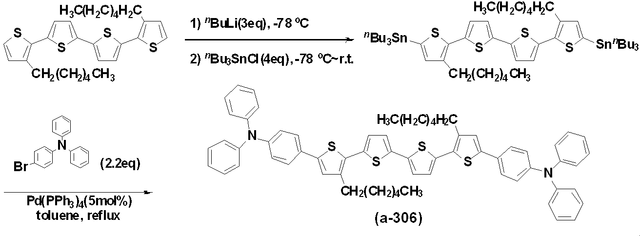
撹拌後、イオン交換水およびノルマルヘキサンを加え分液し、得られた有機層を更にイオン交換水で2回洗浄した後、硫酸ナトリウムを用いて乾燥した。
そして、溶媒を留去して(3,3’’’-ジヘキシル-[2,2’:5’,2’’:5’’,2’’’-クウォーターチオフェン]-5,5’’’-ジイル)ビス(トリブチルスタナン)を含む混合物(3.45g)を得た。
次に、別のフラスコ内に、この得られた混合物3.0gと4-ブロモ-N,N-ジフェニルアニリン1.2gを入れて窒素置換した後、トルエン45mL、テトラキス(トリフェニルホスフィン)パラジウム0.10gを順次加え、還流条件下で8時間撹拌した。
撹拌後、室温まで放冷し、そこへクロロホルムおよびイオン交換水を加えて分液し、得られた有機層を更にイオン交換水で洗浄し、硫酸ナトリウムを用いて乾燥した。
そして、溶媒を留去し、カラムクロマトグラフィーにて精製し、オリゴチオフェン誘導体4を得た(収量:0.76g,収率:44% 2段階通算収率)。
1H-NMR(CDCl3):δ7.44(4H,d,J=8.9Hz),7.28-7.23(m,8H),7.12-7.10(m,10H),7.06-7.00(m,12H),2.78(t,J=7.4Hz,4H),1.69(quint,J=7.4Hz,4H),1.44-1.30(m,12H),0.89(m,6H).
実施例で使用する式(a-34)で表されるオリゴチオフェン誘導体5(以下、TP5ともいう。)を以下の方法により合成した。

その後、再び-78℃に冷却して30分間撹拌した後、トリブチルクロロスタナン8.8mLを滴下して10分撹拌し、次いで0℃に昇温してさらに30分間撹拌した。
撹拌後、反応混合物から減圧下で溶媒を留去し、得られた残渣をトルエンに加え、ろ過によって不溶物を除去し、得られたろ液から減圧下で溶媒を留去し、ターチオフェンのビススタニル体を含むオイル状物12.88g(当該ビススタニル体の純度51.91%)得た。
次いで、窒素雰囲気下で、別のフラスコ内に、このターチオフェンビススタニル体を含むオイル状物6.44g、2-ブロモ-3-ノルマルヘキシルチオフェン2.41g、トルエン24mLおよびテトラキス(トリフェニルホスフィン)パラジウム0.23gを順次入れて、還流条件下4.5時間撹拌した。
室温まで放冷し、溶媒を減圧留去した後、ろ過にて不溶物を除去した。得られたろ液を濃縮し、シリカゲルカラムクロマトグラフィーにて精製し、オリゴチオフェン誘導体5を得た(収量:1.29g、収率:55%、2段階通算収率)。
1H-NMR(CDCl3):7.17(d,J=5.1Hz,2H),7.12(d,J=3.9Hz,2H),7.09(s,2H),7.01(d,J=3.9Hz,2H),6.93(d,J=5.1Hz,2H),2.78(t,J=7.7Hz,4H),1.54-1.70(m,4H),1.28-1.41(m,12H),0.89(t,J=7.0Hz,6H).
[実施例1-1]
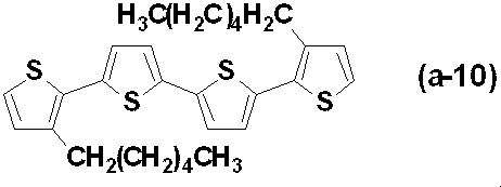
式(a-10)で表されるオリゴチオフェン誘導体(Sigma-Aldrich Co.LLC.製)(以下、TP1ともいう。)0.124gと、リンタングステン酸(関東化学(株)製)0.247gとを、窒素雰囲気下で1,3-ジメチル-2-イミダゾリジノン4.0gに溶解させた。得られた溶液に、シクロヘキサノール6.0gおよびプロピレングリコール2.0gを加えて撹拌し、電荷輸送性ワニスを調製した。
TP1の使用量およびリンタングステン酸の使用量を、それぞれ、0.093gおよび0.278g(実施例1-2)、0.074gおよび0.297g(実施例1-3)、0.062gおよび0.309g(実施例1-4)、0.053gおよび0.318g(実施例1-5)とした以外は、実施例1-1と同様の方法で電荷輸送性ワニスを調製した。
TP1 0.124gの代わりにTP3 0.062gを用い、リンタングステン酸の使用量を0.309gとした以外は、実施例1-1と同様の方法で電荷輸送性ワニスを調製した。
TP3の使用量およびリンタングステン酸の使用量を、それぞれ0.034gおよび0.337g(実施例1-7)、0.018gおよび0.353g(実施例1-8)とした以外は、実施例1-6と同様の方法で電荷輸送性ワニスを調製した。
TP5 0.116gと、リンタングステン酸0.348gとを、窒素雰囲気下で1,3-ジメチル-2-イミダゾリジノン10.5gに溶解させた。得られた溶液に2,3-ブタンジオール3g、プロピレングリコールモノメチルエーテル1.5gを順次加えて撹拌し、電荷輸送性ワニスを調製した。
[実施例2-1~2-5]
実施例1-1~1-5で得られたワニスを、スピンコーターを用いて石英基板に塗布した後、大気中、50℃で5分間乾燥し、さらに230℃で15分間焼成し、石英基板上に膜厚30nmの均一な薄膜を形成した。そして、形成した薄膜の透過率を測定した。透過率は可視領域である波長400~800nmをスキャンした。400~800nmの平均透過率を表1に示す。
なお、石英基板は、プラズマ洗浄装置(150W、30秒間)を用いて表面上の不純物を除却してから使用した。

[実施例3-1]
実施例1-1で得られたワニスを、スピンコーターを用いてITO基板に塗布した後、50℃で5分間乾燥し、さらに、大気雰囲気下、230℃で10分間焼成し、ITO基板上に30nmの均一な薄膜を形成した。ITO基板としては、インジウム錫酸化物(ITO)が表面上に膜厚150nmでパターニングされた25mm×25mm×0.7tのガラス基板を用い、使用前にO2プラズマ洗浄装置(150W、30秒間)によって表面上の不純物を除却した。
次いで、薄膜を形成したITO基板に対し、蒸着装置(真空度1.0×10⁻⁵Pa)を用いてα-NPD、Alq3、フッ化リチウム、およびアルミニウムの薄膜を順次積層し、有機EL素子を得た。この際、蒸着レートは、α-NPD,Alq3およびアルミニウムについては0.2nm/秒、フッ化リチウムについては0.02nm/秒の条件でそれぞれ行い、膜厚は、それぞれ30nm、40nm、0.5nmおよび120nmとした。
なお、空気中の酸素、水等の影響による特性劣化を防止するため、有機EL素子は封止基板により封止した後、その特性を評価した。封止は、以下の手順で行った。
酸素濃度2ppm以下、露点-85℃以下の窒素雰囲気中で、有機EL素子を封止基板の間に収め、封止基板を接着材(ナガセケムテックス(株)製,XNR5516Z-B1)により貼り合わせた。この際、捕水剤(ダイニック(株)製,HD-071010W-40)を有機EL素子と共に封止基板内に収めた。貼り合わせた封止基板に対し、UV光を照射(波長:365nm、照射量:6000mJ/cm2)した後、80℃で1時間、アニーリング処理して接着材を硬化させた。
実施例1-1で得られたワニスの代わりに、それぞれ、実施例1-2~1-9で得られたワニスを用いた以外は、実施例3-1と同様の方法で有機EL素子を作製した。
実施例1-1で得られたワニスの代わりにPEDOT/PSS(H.C.Starck社製AI4083)を用いた以外は、実施例3-1と同様の方法で素子を作製した。

Claims (8)
- 式(1)で表されるオリゴチオフェン誘導体からなる電荷輸送性物質と、ヘテロポリ酸からなるドーパント物質と、有機溶媒とを含むことを特徴とする電荷輸送性ワニス。

Y1~Y6は、互いに独立して、Z1で置換されていてもよい炭素数1~20のアルキル基、Z1で置換されていてもよい炭素数2~20のアルケニル基、Z1で置換されていてもよい炭素数2~20のアルキニル基、Z2で置換されていてもよい炭素数6~20のアリール基、またはZ2で置換されていてもよい炭素数2~20のヘテロアリール基を表し、
Z1は、炭素数6~20のアリール基または炭素数2~20のヘテロアリール基を表し、
Z2は、炭素数1~20のアルキル基、炭素数2~20のアルケニル基または炭素数2~20のアルキニル基を表し、
n1~n3は、互いに独立して、自然数を示し、かつ、4≦n1+n2+n3≦20を満たす。) - 前記オリゴチオフェン誘導体が、式(2)で表される請求項1記載の電荷輸送性ワニス。

- 請求項1または2記載の電荷輸送性ワニスを用いて作製される電荷輸送性薄膜。
- 請求項3記載の電荷輸送性薄膜を有する電子デバイス。
- 請求項3記載の電荷輸送性薄膜を有する有機エレクトロルミネッセンス素子。
- 前記電荷輸送性薄膜が、正孔注入層または正孔輸送層である請求項5記載の有機エレクトロルミネッセンス素子。
- 請求項1または2記載の電荷輸送性ワニスを基材上に塗布して焼成することを特徴とする電荷輸送性薄膜の製造方法。
- 請求項3記載の電荷輸送性薄膜を用いることを特徴とする有機エレクトロルミネッセンス素子の製造方法。
Priority Applications (3)
| Application Number | Priority Date | Filing Date | Title |
|---|---|---|---|
| JP2015517001A JP6132016B2 (ja) | 2013-05-17 | 2014-04-16 | 電荷輸送性ワニス |
| KR1020157034504A KR102219003B1 (ko) | 2013-05-17 | 2014-04-16 | 전하 수송성 바니시 |
| CN201480028599.8A CN105210207A (zh) | 2013-05-17 | 2014-04-16 | 电荷传输性清漆 |
Applications Claiming Priority (2)
| Application Number | Priority Date | Filing Date | Title |
|---|---|---|---|
| JP2013-104776 | 2013-05-17 | ||
| JP2013104776 | 2013-05-17 |
Publications (1)
| Publication Number | Publication Date |
|---|---|
| WO2014185208A1 true WO2014185208A1 (ja) | 2014-11-20 |
Family
ID=51898189
Family Applications (1)
| Application Number | Title | Priority Date | Filing Date |
|---|---|---|---|
| PCT/JP2014/060823 Ceased WO2014185208A1 (ja) | 2013-05-17 | 2014-04-16 | 電荷輸送性ワニス |
Country Status (5)
| Country | Link |
|---|---|
| JP (1) | JP6132016B2 (ja) |
| KR (1) | KR102219003B1 (ja) |
| CN (1) | CN105210207A (ja) |
| TW (1) | TWI650385B (ja) |
| WO (1) | WO2014185208A1 (ja) |
Citations (4)
| Publication number | Priority date | Publication date | Assignee | Title |
|---|---|---|---|---|
| JP2008112904A (ja) * | 2006-10-31 | 2008-05-15 | Idemitsu Kosan Co Ltd | 有機エレクトロルミネッセンス素子 |
| JP2008306170A (ja) * | 2007-05-09 | 2008-12-18 | Toray Ind Inc | 発光素子 |
| WO2010058777A1 (ja) * | 2008-11-19 | 2010-05-27 | 日産化学工業株式会社 | 電荷輸送性材料および電荷輸送性ワニス |
| WO2013042623A1 (ja) * | 2011-09-21 | 2013-03-28 | 日産化学工業株式会社 | 電荷輸送性ワニス |
Family Cites Families (1)
| Publication number | Priority date | Publication date | Assignee | Title |
|---|---|---|---|---|
| KR20110095883A (ko) * | 2008-11-19 | 2011-08-25 | 닛산 가가쿠 고교 가부시키 가이샤 | 전하수송성 재료 및 전하수송성 바니시 |
-
2014
- 2014-04-16 JP JP2015517001A patent/JP6132016B2/ja active Active
- 2014-04-16 WO PCT/JP2014/060823 patent/WO2014185208A1/ja not_active Ceased
- 2014-04-16 TW TW103113865A patent/TWI650385B/zh active
- 2014-04-16 KR KR1020157034504A patent/KR102219003B1/ko active Active
- 2014-04-16 CN CN201480028599.8A patent/CN105210207A/zh active Pending
Patent Citations (4)
| Publication number | Priority date | Publication date | Assignee | Title |
|---|---|---|---|---|
| JP2008112904A (ja) * | 2006-10-31 | 2008-05-15 | Idemitsu Kosan Co Ltd | 有機エレクトロルミネッセンス素子 |
| JP2008306170A (ja) * | 2007-05-09 | 2008-12-18 | Toray Ind Inc | 発光素子 |
| WO2010058777A1 (ja) * | 2008-11-19 | 2010-05-27 | 日産化学工業株式会社 | 電荷輸送性材料および電荷輸送性ワニス |
| WO2013042623A1 (ja) * | 2011-09-21 | 2013-03-28 | 日産化学工業株式会社 | 電荷輸送性ワニス |
Also Published As
| Publication number | Publication date |
|---|---|
| JP6132016B2 (ja) | 2017-05-24 |
| TW201506098A (zh) | 2015-02-16 |
| CN105210207A (zh) | 2015-12-30 |
| JPWO2014185208A1 (ja) | 2017-02-23 |
| KR102219003B1 (ko) | 2021-02-23 |
| KR20160010488A (ko) | 2016-01-27 |
| TWI650385B (zh) | 2019-02-11 |
Similar Documents
| Publication | Publication Date | Title |
|---|---|---|
| JP6459350B2 (ja) | 電荷輸送性ワニス、電荷輸送性薄膜及び有機エレクトロルミネッセンス素子 | |
| JP6414213B2 (ja) | 有機エレクトロルミネッセンス素子の正孔注入層形成用ワニス | |
| JP6763425B2 (ja) | アリールアミン誘導体とその利用 | |
| JP6597597B2 (ja) | アニリン誘導体およびその利用 | |
| JP2019135774A (ja) | 正孔注入層形成用電荷輸送性ワニス | |
| JP6760455B2 (ja) | アニリン誘導体およびその製造方法 | |
| JP6601390B2 (ja) | アニリン誘導体およびその利用 | |
| JP6011723B2 (ja) | トリフェニルアミン誘導体およびその利用 | |
| JP6551693B2 (ja) | 電荷輸送性ワニス、電荷輸送性薄膜及びその製造方法、並びに有機エレクトロルミネッセンス素子及びその製造方法 | |
| JP6061034B2 (ja) | アニリン誘導体、電荷輸送性ワニス及び有機エレクトロルミネッセンス素子 | |
| JP2015092559A (ja) | 電荷輸送性ワニス、電荷輸送性薄膜及び有機エレクトロルミネッセンス素子 | |
| JPWO2015137391A1 (ja) | アニリン誘導体およびその利用 | |
| JP6132016B2 (ja) | 電荷輸送性ワニス | |
| JP6558373B2 (ja) | 電荷輸送性ワニス | |
| WO2018186340A1 (ja) | 電荷輸送性ワニス | |
| JP6601405B2 (ja) | 電荷輸送性ワニス | |
| WO2016006673A1 (ja) | 電荷輸送性ワニス |
Legal Events
| Date | Code | Title | Description |
|---|---|---|---|
| 121 | Ep: the epo has been informed by wipo that ep was designated in this application |
Ref document number: 14797241 Country of ref document: EP Kind code of ref document: A1 |
|
| ENP | Entry into the national phase |
Ref document number: 2015517001 Country of ref document: JP Kind code of ref document: A |
|
| NENP | Non-entry into the national phase |
Ref country code: DE |
|
| ENP | Entry into the national phase |
Ref document number: 20157034504 Country of ref document: KR Kind code of ref document: A |
|
| 122 | Ep: pct application non-entry in european phase |
Ref document number: 14797241 Country of ref document: EP Kind code of ref document: A1 |