WO2014174873A1 - 半導体装置およびその製造方法 - Google Patents
半導体装置およびその製造方法 Download PDFInfo
- Publication number
- WO2014174873A1 WO2014174873A1 PCT/JP2014/052876 JP2014052876W WO2014174873A1 WO 2014174873 A1 WO2014174873 A1 WO 2014174873A1 JP 2014052876 W JP2014052876 W JP 2014052876W WO 2014174873 A1 WO2014174873 A1 WO 2014174873A1
- Authority
- WO
- WIPO (PCT)
- Prior art keywords
- main body
- lead frame
- semiconductor chip
- semiconductor device
- reinforcing
- Prior art date
- Legal status (The legal status is an assumption and is not a legal conclusion. Google has not performed a legal analysis and makes no representation as to the accuracy of the status listed.)
- Ceased
Links
Images



Classifications
-
- H—ELECTRICITY
- H10—SEMICONDUCTOR DEVICES; ELECTRIC SOLID-STATE DEVICES NOT OTHERWISE PROVIDED FOR
- H10W—GENERIC PACKAGES, INTERCONNECTIONS, CONNECTORS OR OTHER CONSTRUCTIONAL DETAILS OF DEVICES COVERED BY CLASS H10
- H10W70/00—Package substrates; Interposers; Redistribution layers [RDL]
- H10W70/40—Leadframes
- H10W70/481—Leadframes for devices being provided for in groups H10D8/00 - H10D48/00
-
- H—ELECTRICITY
- H10—SEMICONDUCTOR DEVICES; ELECTRIC SOLID-STATE DEVICES NOT OTHERWISE PROVIDED FOR
- H10W—GENERIC PACKAGES, INTERCONNECTIONS, CONNECTORS OR OTHER CONSTRUCTIONAL DETAILS OF DEVICES COVERED BY CLASS H10
- H10W70/00—Package substrates; Interposers; Redistribution layers [RDL]
- H10W70/40—Leadframes
- H10W70/464—Additional interconnections in combination with leadframes
-
- H—ELECTRICITY
- H10—SEMICONDUCTOR DEVICES; ELECTRIC SOLID-STATE DEVICES NOT OTHERWISE PROVIDED FOR
- H10W—GENERIC PACKAGES, INTERCONNECTIONS, CONNECTORS OR OTHER CONSTRUCTIONAL DETAILS OF DEVICES COVERED BY CLASS H10
- H10W74/00—Encapsulations, e.g. protective coatings
- H10W74/01—Manufacture or treatment
- H10W74/016—Manufacture or treatment using moulds
-
- H—ELECTRICITY
- H10—SEMICONDUCTOR DEVICES; ELECTRIC SOLID-STATE DEVICES NOT OTHERWISE PROVIDED FOR
- H10W—GENERIC PACKAGES, INTERCONNECTIONS, CONNECTORS OR OTHER CONSTRUCTIONAL DETAILS OF DEVICES COVERED BY CLASS H10
- H10W74/00—Encapsulations, e.g. protective coatings
- H10W74/10—Encapsulations, e.g. protective coatings characterised by their shape or disposition
- H10W74/111—Encapsulations, e.g. protective coatings characterised by their shape or disposition the semiconductor body being completely enclosed
-
- H—ELECTRICITY
- H10—SEMICONDUCTOR DEVICES; ELECTRIC SOLID-STATE DEVICES NOT OTHERWISE PROVIDED FOR
- H10W—GENERIC PACKAGES, INTERCONNECTIONS, CONNECTORS OR OTHER CONSTRUCTIONAL DETAILS OF DEVICES COVERED BY CLASS H10
- H10W72/00—Interconnections or connectors in packages
- H10W72/071—Connecting or disconnecting
- H10W72/073—Connecting or disconnecting of die-attach connectors
-
- H—ELECTRICITY
- H10—SEMICONDUCTOR DEVICES; ELECTRIC SOLID-STATE DEVICES NOT OTHERWISE PROVIDED FOR
- H10W—GENERIC PACKAGES, INTERCONNECTIONS, CONNECTORS OR OTHER CONSTRUCTIONAL DETAILS OF DEVICES COVERED BY CLASS H10
- H10W72/00—Interconnections or connectors in packages
- H10W72/071—Connecting or disconnecting
- H10W72/075—Connecting or disconnecting of bond wires
- H10W72/07551—Connecting or disconnecting of bond wires characterised by changes in properties of the bond wires during the connecting
- H10W72/07552—Connecting or disconnecting of bond wires characterised by changes in properties of the bond wires during the connecting changes in structures or sizes
-
- H—ELECTRICITY
- H10—SEMICONDUCTOR DEVICES; ELECTRIC SOLID-STATE DEVICES NOT OTHERWISE PROVIDED FOR
- H10W—GENERIC PACKAGES, INTERCONNECTIONS, CONNECTORS OR OTHER CONSTRUCTIONAL DETAILS OF DEVICES COVERED BY CLASS H10
- H10W72/00—Interconnections or connectors in packages
- H10W72/071—Connecting or disconnecting
- H10W72/075—Connecting or disconnecting of bond wires
- H10W72/07551—Connecting or disconnecting of bond wires characterised by changes in properties of the bond wires during the connecting
- H10W72/07554—Connecting or disconnecting of bond wires characterised by changes in properties of the bond wires during the connecting changes in dispositions
-
- H—ELECTRICITY
- H10—SEMICONDUCTOR DEVICES; ELECTRIC SOLID-STATE DEVICES NOT OTHERWISE PROVIDED FOR
- H10W—GENERIC PACKAGES, INTERCONNECTIONS, CONNECTORS OR OTHER CONSTRUCTIONAL DETAILS OF DEVICES COVERED BY CLASS H10
- H10W72/00—Interconnections or connectors in packages
- H10W72/30—Die-attach connectors
- H10W72/321—Structures or relative sizes of die-attach connectors
- H10W72/325—Die-attach connectors having a filler embedded in a matrix
-
- H—ELECTRICITY
- H10—SEMICONDUCTOR DEVICES; ELECTRIC SOLID-STATE DEVICES NOT OTHERWISE PROVIDED FOR
- H10W—GENERIC PACKAGES, INTERCONNECTIONS, CONNECTORS OR OTHER CONSTRUCTIONAL DETAILS OF DEVICES COVERED BY CLASS H10
- H10W72/00—Interconnections or connectors in packages
- H10W72/30—Die-attach connectors
- H10W72/351—Materials of die-attach connectors
- H10W72/352—Materials of die-attach connectors comprising metals or metalloids, e.g. solders
-
- H—ELECTRICITY
- H10—SEMICONDUCTOR DEVICES; ELECTRIC SOLID-STATE DEVICES NOT OTHERWISE PROVIDED FOR
- H10W—GENERIC PACKAGES, INTERCONNECTIONS, CONNECTORS OR OTHER CONSTRUCTIONAL DETAILS OF DEVICES COVERED BY CLASS H10
- H10W72/00—Interconnections or connectors in packages
- H10W72/50—Bond wires
- H10W72/521—Structures or relative sizes of bond wires
- H10W72/527—Multiple bond wires having different sizes
-
- H—ELECTRICITY
- H10—SEMICONDUCTOR DEVICES; ELECTRIC SOLID-STATE DEVICES NOT OTHERWISE PROVIDED FOR
- H10W—GENERIC PACKAGES, INTERCONNECTIONS, CONNECTORS OR OTHER CONSTRUCTIONAL DETAILS OF DEVICES COVERED BY CLASS H10
- H10W72/00—Interconnections or connectors in packages
- H10W72/50—Bond wires
- H10W72/531—Shapes of wire connectors
- H10W72/533—Cross-sectional shape
- H10W72/534—Cross-sectional shape being rectangular
-
- H—ELECTRICITY
- H10—SEMICONDUCTOR DEVICES; ELECTRIC SOLID-STATE DEVICES NOT OTHERWISE PROVIDED FOR
- H10W—GENERIC PACKAGES, INTERCONNECTIONS, CONNECTORS OR OTHER CONSTRUCTIONAL DETAILS OF DEVICES COVERED BY CLASS H10
- H10W72/00—Interconnections or connectors in packages
- H10W72/50—Bond wires
- H10W72/541—Dispositions of bond wires
- H10W72/547—Dispositions of multiple bond wires
-
- H—ELECTRICITY
- H10—SEMICONDUCTOR DEVICES; ELECTRIC SOLID-STATE DEVICES NOT OTHERWISE PROVIDED FOR
- H10W—GENERIC PACKAGES, INTERCONNECTIONS, CONNECTORS OR OTHER CONSTRUCTIONAL DETAILS OF DEVICES COVERED BY CLASS H10
- H10W72/00—Interconnections or connectors in packages
- H10W72/50—Bond wires
- H10W72/551—Materials of bond wires
- H10W72/552—Materials of bond wires comprising metals or metalloids, e.g. silver
- H10W72/5522—Materials of bond wires comprising metals or metalloids, e.g. silver comprising gold [Au]
-
- H—ELECTRICITY
- H10—SEMICONDUCTOR DEVICES; ELECTRIC SOLID-STATE DEVICES NOT OTHERWISE PROVIDED FOR
- H10W—GENERIC PACKAGES, INTERCONNECTIONS, CONNECTORS OR OTHER CONSTRUCTIONAL DETAILS OF DEVICES COVERED BY CLASS H10
- H10W72/00—Interconnections or connectors in packages
- H10W72/50—Bond wires
- H10W72/551—Materials of bond wires
- H10W72/552—Materials of bond wires comprising metals or metalloids, e.g. silver
- H10W72/5524—Materials of bond wires comprising metals or metalloids, e.g. silver comprising aluminium [Al]
-
- H—ELECTRICITY
- H10—SEMICONDUCTOR DEVICES; ELECTRIC SOLID-STATE DEVICES NOT OTHERWISE PROVIDED FOR
- H10W—GENERIC PACKAGES, INTERCONNECTIONS, CONNECTORS OR OTHER CONSTRUCTIONAL DETAILS OF DEVICES COVERED BY CLASS H10
- H10W72/00—Interconnections or connectors in packages
- H10W72/851—Dispositions of multiple connectors or interconnections
- H10W72/874—On different surfaces
- H10W72/884—Die-attach connectors and bond wires
-
- H—ELECTRICITY
- H10—SEMICONDUCTOR DEVICES; ELECTRIC SOLID-STATE DEVICES NOT OTHERWISE PROVIDED FOR
- H10W—GENERIC PACKAGES, INTERCONNECTIONS, CONNECTORS OR OTHER CONSTRUCTIONAL DETAILS OF DEVICES COVERED BY CLASS H10
- H10W74/00—Encapsulations, e.g. protective coatings
-
- H—ELECTRICITY
- H10—SEMICONDUCTOR DEVICES; ELECTRIC SOLID-STATE DEVICES NOT OTHERWISE PROVIDED FOR
- H10W—GENERIC PACKAGES, INTERCONNECTIONS, CONNECTORS OR OTHER CONSTRUCTIONAL DETAILS OF DEVICES COVERED BY CLASS H10
- H10W74/00—Encapsulations, e.g. protective coatings
- H10W74/10—Encapsulations, e.g. protective coatings characterised by their shape or disposition
- H10W74/111—Encapsulations, e.g. protective coatings characterised by their shape or disposition the semiconductor body being completely enclosed
- H10W74/127—Encapsulations, e.g. protective coatings characterised by their shape or disposition the semiconductor body being completely enclosed characterised by arrangements for sealing or adhesion
-
- H—ELECTRICITY
- H10—SEMICONDUCTOR DEVICES; ELECTRIC SOLID-STATE DEVICES NOT OTHERWISE PROVIDED FOR
- H10W—GENERIC PACKAGES, INTERCONNECTIONS, CONNECTORS OR OTHER CONSTRUCTIONAL DETAILS OF DEVICES COVERED BY CLASS H10
- H10W90/00—Package configurations
- H10W90/701—Package configurations characterised by the relative positions of pads or connectors relative to package parts
- H10W90/731—Package configurations characterised by the relative positions of pads or connectors relative to package parts of die-attach connectors
- H10W90/736—Package configurations characterised by the relative positions of pads or connectors relative to package parts of die-attach connectors between a chip and a stacked lead frame, conducting package substrate or heat sink
-
- H—ELECTRICITY
- H10—SEMICONDUCTOR DEVICES; ELECTRIC SOLID-STATE DEVICES NOT OTHERWISE PROVIDED FOR
- H10W—GENERIC PACKAGES, INTERCONNECTIONS, CONNECTORS OR OTHER CONSTRUCTIONAL DETAILS OF DEVICES COVERED BY CLASS H10
- H10W90/00—Package configurations
- H10W90/701—Package configurations characterised by the relative positions of pads or connectors relative to package parts
- H10W90/751—Package configurations characterised by the relative positions of pads or connectors relative to package parts of bond wires
- H10W90/756—Package configurations characterised by the relative positions of pads or connectors relative to package parts of bond wires between a chip and a stacked lead frame, conducting package substrate or heat sink
Definitions
- the present invention relates to a semiconductor device of a full mold package and a manufacturing method thereof.
- the lead frame when injecting a sealing material into a mold that houses a main part of the semiconductor device when manufacturing the semiconductor device, the lead frame is deformed by the pressure of the injected sealing material. May end up.
- the thickness of the sealing material on the back surface side (the side on which no semiconductor chip is mounted) of the lead frame is thin in order to improve heat dissipation.
- the lead frame has a sealing material injection port more than the predetermined position.
- the lead frame In the case of floating on the side opposite to the side where the Further, when the sealing material injection port is disposed on the surface side of the lead frame (the side on which the semiconductor chip is mounted), the lead frame is on the side opposite to the side where the sealing material injection port is provided rather than the predetermined position. It may warp.
- Patent Document 1 discloses a manufacturing method of a fixed pin method in which a lead frame is continuously fixed by a pin during a sealing material injection period.
- Japanese public utility model publication Japanese Public utility model publication "Japanese Utility Model Publication No. 62-63944 (published April 21, 1987)"
- the sealing material is cured in a state where the fixed pin and the lead frame are in contact with each other. Therefore, when the mold and the fixed pin are removed, the region in contact with the fixed pin in the lead frame is exposed. End up. For this reason, dielectric breakdown may occur from the exposed portion.
- the pins for fixing the lead frame are made movable, the lead frame is fixed by the pins when the sealing material is injected, and the pins are separated from the lead frame before the injected sealing material is hardened and hardened. It is conceivable to use a movable pin type manufacturing method in which a sealing material is also introduced into an area of the frame that has been in contact with the pin and the area is covered with the sealing material.
- the movable pin method has a problem that the manufacturing apparatus becomes expensive because it is necessary to provide a mechanism for moving the movable pin.
- the present invention has been made to solve the above-described problems, and an object of the present invention is to manufacture a semiconductor device of a full mold package having high insulation properties with a simple configuration.
- a semiconductor device includes a lead frame having a plate-like main body portion and a lead terminal portion connected to one end of the main body portion, and is mounted on the main body portion and electrically connected to the lead frame.
- a reinforcing member that reinforces the lead frame is attached to the part of the lead terminal portion and the other end is attached to the main body portion or a member mounted on the main body portion.
- a highly insulating semiconductor device can be realized easily and inexpensively.
- FIG. 2 is a cross-sectional view of the semiconductor device 100a according to the present embodiment.
- a semiconductor device 100a includes a lead frame 2, a semiconductor chip 1 bonded on the lead frame 2 with an adhesive layer 3, and a bonding wire for electrically connecting the semiconductor chip 1 and the lead frame 2. 4, a reinforcing wire 5 a having one end attached to the lead frame 2 and the other end attached to the semiconductor chip 1, and a sealing portion 6.
- the lead frame 2 includes a main body portion 2a, a lead terminal portion 2b, and a connection portion 2c that connects one end of the main body portion 2a and one end of the lead terminal portion 2b.
- the main body 2a is made of a plate-like member, and the semiconductor chip 1 is mounted on one surface of the main body 2a via the adhesive layer 3.
- the semiconductor chip 1 and the main body 2a are electrically connected by a bonding wire 4.
- One end of the lead terminal portion 2b, the upper surface of the semiconductor chip 1 mounted on the main body portion 2a (surface opposite to the main body portion 2a) and the upper surface of the lead terminal portion 2b (surface on the side where the semiconductor chip 1 is mounted) Are connected to the end of the main body 2a by the connecting portion 2c so that they are substantially flush with each other.
- the material of the lead frame 2 (the body portion 2a, the lead terminal portion 2b, and the connection portion 2c) is not particularly limited as long as it is a material having electrical conductivity. For example, silver, copper, aluminum, or the like is used. Metal can be used.
- the lead frame 2 may be made of a material having thermal conductivity for radiating the heat of the semiconductor chip 1 to the outside of the semiconductor device 100a.
- the main body 2a, the lead terminal 2b, and the connection 2c may be formed by bending a single member or the like, and are formed by joining separate members. May be.
- the configuration and material of the semiconductor chip 1 are not particularly limited, and various conventionally known semiconductor chips can be used.
- a semiconductor chip 1 made of silicon may be used.
- the arrangement method is not particularly limited. For example, (i) a plurality of semiconductor chips may be arranged in different regions on the lead frame 2, and (ii) ) A plurality of semiconductor chips may be stacked (stacked) on the lead frame 2, and (iii) semiconductor chip groups formed by stacking a plurality of semiconductor chips are arranged in a plurality of different regions on the lead frame 2. Also good.
- Each semiconductor chip may be electrically connected to the lead frame 2 individually, or the semiconductor chips may be electrically connected to each other.
- the connection method for electrically connecting between the semiconductor chip and the lead frame 2 and between the semiconductor chips is not particularly limited. For example, a conventionally known method such as wire bonding is used. Can do.
- the present invention the configuration in which the semiconductor chip 1 is mounted only on one side (front side) of the lead frame 2 has been described.
- the present invention is not limited to this, and the semiconductor chip 1 is formed on both sides of the lead frame 2. May be installed.
- the adhesive layer 3 is for adhering the semiconductor chip 1 to the lead frame 2.
- the material and shape of the adhesive layer 3 are not particularly limited as long as the lead frame 2 and the semiconductor chip 1 can be appropriately bonded.
- solid, liquid, paste, sheet, etc. It may be of any form.
- a known material such as solder or Ag (silver) paste may be used.
- the semiconductor chip 1 and the lead frame 2 may be electrically connected to each other via the adhesive layer 3, and in that case, a conductive material may be used as the adhesive layer 3.
- a nonconductive material may be used as the adhesive layer 3.
- the semiconductor chip 1 is mounted on the lead frame 2 by bonding, but the method for attaching the semiconductor chip 1 to the lead frame 2 is not particularly limited.
- the bonding wire 4 electrically connects the semiconductor chip 1 and the lead frame 2.
- the semiconductor chips 1 may be electrically connected by bonding wires 4.
- the material of the bonding wire 4 is not particularly limited as long as it has conductivity, and conventionally known materials such as gold and aluminum can be used.
- the semiconductor chip 1 and the lead frame 2 are connected by the wire bonding method.
- the method for connecting the semiconductor chip 1 and the lead frame 2 is not particularly limited. A bond method or the like may be used.
- the reinforcing wire (reinforcing member) 5a is a linear member having one end attached to the semiconductor chip 1 and the other end attached to a part of the lead terminal portion 2b of the lead frame 2 (portion covered by the sealing portion 6). Consists of. In the present embodiment, aluminum reinforcing wires are attached to the semiconductor chip 1 and the lead frame 2 (lead terminal portion 2b) by a bonding method. However, the material, shape, and number of the reinforcing wires 5a are floated on the lead frame 2 by the pressure caused by the injection of the sealing material when the sealing material is injected in the manufacturing process of the semiconductor device 100a (at least part of the lead frame).
- the reinforcing wire 5a made of a highly rigid material may be used, the rigidity may be increased by increasing the diameter of the reinforcing wire 5a, or the rigidity may be increased by providing a plurality of reinforcing wires 5a.
- members for example, a plate-shaped member, a rod-shaped member, a linear member, or a member that combined them
- the same material for example, gold or aluminum
- the bonding wire 4 may be used as the reinforcing wire 5a.
- the attaching process of the bonding wire 4 and the attaching process of the reinforcing wire 5a are performed in a common process. It may be.
- the reinforcing wire 5a may function as a signal line for signal transmission between the semiconductor chip 1 and the lead frame 2.
- the number of members can be reduced and the configuration of the semiconductor device 100a can be simplified as compared with the case where the signal line and the reinforcing wire 5a are provided separately, and the cost can be reduced.
- the sealing part 6 covers a main part (a part excluding a part of the lead terminal part 2b) of the semiconductor device 100a, thereby providing electrical insulation between the main part and the outside. Further, the sealing part 6 includes members (semiconductor chip 1, adhesive layer 3, main body part 2a, connection part 2c, part of lead terminal part 2b, bonding wire 4, reinforcing wire 5a) included in the main part, and It also has a function of protecting the connecting portions of these members from the outside.
- the full mold type sealing structure is formed by forming the sealing portion 6 that covers both surfaces of the main body portion 2a by using the transfer molding method.
- the material of the sealing portion 6 is not particularly limited as long as it has fluidity and curability that can use the transfer molding method and has electrical insulation.
- conventionally known materials such as silicon resins, acrylic resins, and epoxy resins can be used.
- FIG. 1 is an explanatory view showing a process of forming the sealing portion 6.
- the main part (sealing) of the semiconductor device 100 a is placed in the sealing material filling space 14 formed between the upper mold 11 and the lower mold 12.
- the portion covered by the portion 6 that is, the semiconductor chip 1, the adhesive layer 3, the main body portion 2a, the connection portion 2c, a part of the lead terminal portion 2b, the bonding wire 4, and the reinforcing wire 5a
- the lead terminal portion 2 b of the lead frame 2 is sandwiched between the mold 11 and the lower mold 12.
- the lead frame 2 is supported in a cantilever state in which the lead terminal portion 2b sandwiched between the upper die 11 and the lower die 12 serves as a fixed end and the main body 2a side serves as a free end.
- an injection step of injecting the sealing material from the sealing material injection port 13 formed in the lower mold 12 is performed.
- the sealing material injected into the filling space 14 from the sealing material inlet 13 is mounted on the surface side of the lead frame 2 (main body portion 2a) (the semiconductor chip 1 is mounted). And the filling space 14 is filled.
- the lead frame 2 is reinforced by the reinforcing wire 5a, the deformation (floating or warping) of the lead frame 2 due to the pressure accompanying the injection of the sealing material can be prevented.
- the curing step may be performed according to the type of the sealing material.
- the curing step may be a step of curing by leaving for a predetermined time, or a step of curing by heating or cooling. It may be a step of curing by irradiating light such as ultraviolet rays.
- the semiconductor device 100a includes the reinforcing wire 5a for preventing the deformation of the lead frame 2 having one end attached to the lead frame 2 and the other end attached to the semiconductor chip 1. ing.
- the thickness of the sealing portion 6 (distance from the lead frame 2 to the outer surface of the sealing portion 6) can be made constant. The property can be kept uniform regardless of the position.
- the thickness of the sealing portion 6 on the back side (the side on which the semiconductor chip 2 is not mounted) of the lead frame 2 can be made thin and constant, the heat dissipation of the semiconductor device 100a can be improved.
- the sealing material injection port 13 is provided on the header side of the semiconductor device 100a (the tip side of the main body portion 2a (the side far from the lead terminal portion 2b)).
- the lead frame 2 is provided below the lead frame 2.
- the pressure due to the injection of the sealing material mainly acts in the direction of pushing up the lead frame 2 from below the lead frame 2, so that the lead frame 2 floats (deformation in the direction of pushing up the lead frame 2 upward). Prone to occur.
- the deformation (floating) of the lead frame 2 can be prevented or suppressed without using a fixed pin or a movable pin.
- the deformation amount (floating amount) of the lead frame 2 compared to a configuration without the reinforcing wire 5a. ) could be reduced to about 1/5.
- the sealing material injection port 13 is provided on the header side of the semiconductor device 100a (the tip side of the main body 2a (the side far from the lead terminal 2b)) and below the lead frame 2.
- the present invention is not limited to this, and the position of the sealing material inlet 13 may be arbitrarily set.
- the sealing material inlet 13 may be provided on the lead terminal portion 2b side of the semiconductor device 100a or may be provided above the lead frame 2.
- you may provide the sealing material injection port 13 in multiple places.
- FIG. 3 is a cross-sectional view of the semiconductor device 100b according to the present embodiment. The difference from the semiconductor device 100a shown in the first embodiment is that a reinforcing wire 5b is provided instead of the reinforcing wire 5a.
- the reinforcing wire 5a having one end attached to a part of the lead terminal portion 2b of the lead frame 2 and the other end attached to the semiconductor chip 1 is used.
- one end side is attached to a part of the lead terminal portion 2b of the lead frame 2 (portion covered by the sealing portion 6), and the other end side is the lead frame.
- the reinforcing wire 5b attached to the front end side (the side far from the lead terminal portion 2b) of the region 2 of the main body 2a where the semiconductor chip 1 is mounted is used.
- the lead frame 2 can be prevented from being deformed by the injection of the sealing material as in the first embodiment. Further, as compared with the case where the reinforcing wire is attached to the semiconductor chip 1 as in the first embodiment, it is possible to prevent the semiconductor chip 1 from being loaded.
- the other end side of the reinforcing wire 5b is attached to the tip side from the region where the semiconductor chip 1 is mounted in the main body portion 2a. In this way, by attaching the other end of the reinforcing wire 5b to a position far from the lead terminal portion 2b, the deformation suppressing effect of the lead frame 2 can be enhanced.
- the attachment position of the reinforcing wire in this embodiment is not limited to this.
- one end side is attached to a part of the lead terminal portion 2b of the lead frame 2 (portion covered by the sealing portion 6) and the other end You may use the reinforcement wire 5c attached to the lead terminal part 2b side rather than the area
- the reinforcing wire 5c interferes with other wires such as the semiconductor chip 1 and the bonding wire 4 as compared with the case where the reinforcing wire 5b attached to the region on the tip side of the semiconductor chip 1 in the main body 2a is used. Can be easily avoided.
- a more optimal position may be selected according to the structure and characteristics of the semiconductor device.
- the reinforcing wire 5a shown in the first embodiment may be provided.
- FIG. 5 is a cross-sectional view of the semiconductor device 100d according to the present embodiment. The difference from the semiconductor devices 100b and 100c shown in the second embodiment is that a reinforcing wire 5d is provided instead of the reinforcing wires 5b and 5c.
- one end side is attached to a part of the lead terminal portion 2b of the lead frame 2, and the other end side is attached to the surface side (the side on which the semiconductor chip 1 is mounted) of the main body portion 2a of the lead frame 2.
- Reinforcing wires 5b and 5c were used.
- one end side is attached to a part of the lead terminal portion 2b of the lead frame 2 (portion covered by the sealing portion 6), and the other end side is a lead.
- the reinforcing wire 5d attached to the back surface side (the side where the semiconductor chip 1 is not mounted) in the main body 2a of the frame 2 is used.
- the lead frame 2 can be prevented from being deformed by the injection of the sealing material, as in the above-described embodiments.
- the reinforcing wire 5d by attaching the reinforcing wire 5d to the back side (the side where the semiconductor chip 1 is not mounted) of the main body 2a, it is easy for the reinforcing wire 5d to interfere with other members such as the semiconductor chip 1 and the bonding wire 4. Can be avoided.
- the semiconductor chip 1 is mounted only on the front surface side of the main body 2a.
- the present invention is not limited to this.
- the semiconductor chip 1 is mounted on both the front surface side and the back surface side. May be.
- the attachment position of the reinforcing wire 5d to the main body 2a on the other end side is the tip side (lead) relative to the region where the semiconductor chip 1 is attached. It may be on the side far from the terminal portion 2b) or on the lead terminal portion 2b side.
- any one or more of the above-described reinforcing wires 5a, 5b, 5c may be provided.
- FIG. 6 is a cross-sectional view of the semiconductor device 100e according to the present embodiment. The difference from the semiconductor device 100a shown in the first embodiment is that two reinforcing wires 5e and 5e are provided instead of the reinforcing wire 5a.
- Embodiment 1 only one reinforcing wire 5 a having one end attached to the lead terminal portion 2 b of the lead frame 2 and the other end attached to the semiconductor chip 1 is used.
- two reinforcing wires 5e and 5e having one end attached to the lead terminal portion 2b of the lead frame 2 and the other end attached to the semiconductor chip 1 are provided. Used.
- the effect of suppressing the deformation of the lead frame 2 can be enhanced as compared with the case where only one reinforcing wire is used. Even when a relatively thin wire is used as the reinforcing wire 5e, the effect of suppressing the deformation of the lead frame 2 can be enhanced by using the two reinforcing wires 5e.
- reinforcing wires 5e and 5e are used.
- the number of reinforcing wires is not limited to this, and three or more reinforcing wires may be used.
- each reinforcing wire 5e is attached to the semiconductor chip 1.
- the present invention is not limited to this.
- the other end side of each reinforcing wire 5e is connected to the surface side of the main body 2a. It may be attached to the back surface of the main body 2a.
- FIG. 7 is a perspective view of the semiconductor device 100f according to the present embodiment.
- the semiconductor device 100f includes three lead terminal portions 2b 1 , 2b 2 , 2b 3 .
- a bonding wire 4 for electrically connecting the lead frame 2 and the semiconductor chip 1 is connected to the lead terminal portions 2b 1 and 2b 2 , and one end side of the reinforcing wire 5f is connected to the lead terminal portion 2b 3. It is attached. That is, in this embodiment, one end of the stiffening wire 5f is attached to a dedicated lead terminal portion 2b 3 to the reinforcing wire 5f. The other end side of the reinforcing wire 5f is attached to the semiconductor chip 1.
- the other end of the reinforcing wire 5f is attached to the semiconductor chip 1.
- the present invention is not limited to this. . It is also possible to attach a plurality of reinforcing wires to the lead terminal portion 2b 3.
- present embodiment may be combined with any one of the above-described embodiments, and may include any one or more of the reinforcing wires 5a to 5e in addition to the reinforcing wire 5f.
- a semiconductor device includes a lead frame having a plate-like main body portion and a lead terminal portion connected to one end of the main body portion, and is mounted on the main body portion and electrically connected to the lead frame.
- a reinforcing member that reinforces the lead frame is attached to the part of the lead terminal portion and the other end is attached to the main body portion or a member mounted on the main body portion.
- the reinforcing member by providing the reinforcing member, it is possible to prevent the lead frame from floating or warping due to the injection of the sealing material, so that the thickness of the sealing portion formed on the lead frame is made constant.
- a highly insulating semiconductor device can be realized.
- there is no need to provide a mechanism for moving the movable pin as in the conventional movable pin method there is no increase in cost of the manufacturing apparatus. Therefore, a highly insulating semiconductor device can be realized easily and inexpensively.
- the thickness of the sealing portion formed on the lead frame can be made uniform, heat dissipation from the lead frame to the outside of the sealing portion can be improved.
- the reinforcing member has a configuration in which the other end is attached to the semiconductor chip.
- a highly insulating semiconductor device can be realized easily and inexpensively.
- the reinforcing member is made of a conductive material and functions as a signal line for signal transmission between the semiconductor chip and the lead frame. It is a configuration.
- the number of members can be reduced and the configuration of the semiconductor device can be simplified as compared with the case where the signal line and the reinforcing member are provided separately, and the cost can be reduced.
- the semiconductor chip is mounted on one surface of the main body, and the reinforcing member is attached to the one surface of the main body. It is the composition which is.
- a highly insulating semiconductor device can be realized easily and inexpensively. Further, it is possible to prevent a load from being applied to the semiconductor chip as compared with the case where the other end side of the reinforcing member is attached to the semiconductor chip.
- a semiconductor device according to an aspect 5 of the present invention is the semiconductor device according to the aspect 1, wherein the semiconductor chip is mounted on one surface of the main body, and the reinforcing member is attached to the other surface of the main body. It is the composition which is.
- a highly insulating semiconductor device can be realized easily and inexpensively. Further, it is possible to prevent a load from being applied to the semiconductor chip as compared with the case where the other end of the reinforcing member is attached to the semiconductor chip. In addition, it is possible to prevent the reinforcing member from interfering with a bonding wire or the like that connects the semiconductor chip and the lead frame.
- the semiconductor device according to Aspect 6 of the present invention is any one of Aspects 1 to 4, wherein the reinforcing member is composed of a plurality of wire members.
- a semiconductor device includes the plurality of lead terminal portions according to any one of the above aspects 1 to 4, and the reinforcing member is provided on the sealing portion among the plurality of lead terminal portions. It is the structure attached to the dummy terminal part which was coat
- the reinforcing member can be prevented from interfering with a bonding wire or the like that connects the semiconductor chip and the lead frame.
- a method of manufacturing a semiconductor device includes a lead frame having a plate-like main body and a lead terminal connected to one end of the main body, and the lead frame mounted on the main body.
- a semiconductor device manufacturing method comprising: a semiconductor chip electrically connected to a semiconductor chip; and a sealing portion in which the main body portion, the semiconductor chip, and a part of the lead terminal portion are covered with an electrically insulating material.
- An arrangement step of arranging a portion, the semiconductor chip, a part of the lead terminal portion, and the reinforcing member in a filling space filled with a sealing material for forming the sealing portion in a mold, and the filling Sky It is characterized in that it comprises an injection step of injecting the sealant into.
- the reinforcing member by providing the reinforcing member, it is possible to prevent the lead frame from floating or warping due to the injection of the sealing material, so that the thickness of the sealing portion formed on the lead frame is constant. Therefore, a highly insulating semiconductor device can be realized. In addition, it is possible to prevent the problem that the region that is in contact with the fixing pin in the lead frame in the conventional fixing pin method is exposed without being covered with the sealing material. Further, since there is no need to provide a mechanism for moving the movable pin as in the conventional movable pin method, there is no increase in cost of the manufacturing apparatus. Therefore, a highly insulating semiconductor device can be realized easily and inexpensively. In addition, since the thickness of the sealing portion formed on the lead frame can be made uniform, heat dissipation from the lead frame to the outside of the sealing portion can be improved.
- the present invention can be applied to a semiconductor device of a full mold package having a lead frame and a manufacturing method thereof.
Landscapes
- Structures Or Materials For Encapsulating Or Coating Semiconductor Devices Or Solid State Devices (AREA)
Abstract
本体部(2a)と本体部(2a)の一端側に接続されたリード端子部(2b)とを有するリードフレーム(2)と、本体部(2a)に搭載され、リードフレーム(2)に電気的に接続された半導体チップ(1)とを備えた半導体装置において、封止材を注入する前に、一端側がリード端子部(2b)に取り付けられ、他端側が本体部(2a)または本体部(2a)に搭載された部材に取り付けられた補強部材を設ける。
Description
本発明は、フルモールドパッケージの半導体装置およびその製造方法に関するものである。
従来、高耐圧用途等で使用される半導体装置として、半導体装置の主要部(半導体装置を外部に接続するためのリード端子を除く部分)を封止体で被覆することにより高い絶縁性を実現したフルモールドパッケージの半導体装置が知られている。
ところで、フルモールドパッケージの半導体装置では、半導体装置の製造時に半導体装置の主要部を内部に収容した金型内に封止材を注入する際、注入された封止材による圧力でリードフレームが変形してしまう場合がある。特に、フルモールドパッケージの半導体装置では、一般に、放熱性を高めるためにリードフレームの裏面側(半導体チップが搭載されていない側)の封止材の厚みが薄く形成される傾向がある。ところが、裏面側に薄くかつ均一な厚さの封止材を適切に注入するために封止材注入口を裏面側の金型に設けた場合、リードフレームが所定位置よりも封止材注入口が設けられている側とは反対側に浮く場合にある。また、封止材注入口をリードフレームの表面側(半導体チップが搭載されている側)に配置すると、リードフレームが所定位置よりも封止材注入口が設けられている側とは反対側に反る場合がある。
このため、従来のフルモールドパッケージの半導体装置の製造方法では、金型内のリードフレームをピンで固定した状態で封止体の注入を行う方法が用いられている。
例えば、特許文献1には、封止材の注入期間中にリードフレームをピンにより固定し続ける固定ピン方式の製造方法が開示されている。
しかしながら、固定ピン方式の場合、固定ピンとリードフレームとが接触した状態で封止材が硬化するため、金型および固定ピンを取り外したときに、リードフレームにおける固定ピンと接触していた領域が露出してしまう。このため、上記の露出部分から絶縁破壊が生じてしまう可能性がある。
そこで、リードフレームを固定するピンを可動式とし、封止材の注入時にはピンによってリードフレームを固定し、注入した封止材が硬化して固まる前にピンをリードフレームから離間させることにより、リードフレームにおけるピンと接触していた領域にも封止材を入り込ませて当該領域についても封止材で被覆させる、可動ピン方式の製造方法を用いることが考えられる。
しかしながら、可動ピン方式では、可動ピンを移動させるための機構を設ける必要があるので、製造装置が高価になるという問題がある。
本発明は、上記の問題を解決するためになされたものであり、その目的は、絶縁性の高いフルモールドパッケージの半導体装置を簡易な構成で製造することにある。
本発明の一態様にかかる半導体装置は、板状の本体部と上記本体部の一端側に接続されたリード端子部とを有するリードフレームと、上記本体部に搭載され、上記リードフレームに電気的に接続された半導体チップと、上記本体部と上記半導体チップと上記リード端子部の一部とを電気絶縁性を有する材料で被覆した封止部とを備えた半導体装置であって、一端側が上記リード端子部の上記一部に取り付けられ、他端側が上記本体部または上記本体部に搭載された部材に取り付けられた、上記リードフレームを補強する補強部材を備えていることを特徴としている。
上記の本発明の一態様にかかる半導体装置によれば、絶縁性の高い半導体装置を容易かつ安価に実現することができる。
〔実施形態1〕
本発明の一実施形態について説明する。
本発明の一実施形態について説明する。
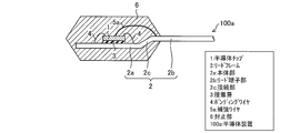
図2は、本実施形態にかかる半導体装置100aの断面図である。この図に示すように、半導体装置100aは、リードフレーム2と、リードフレーム2上に接着層3によって接着された半導体チップ1と、半導体チップ1とリードフレーム2とを電気的に接続するボンディングワイヤ4と、一端側がリードフレーム2に取り付けられ、他端側が半導体チップ1に取り付けられた補強ワイヤ5aと、封止部6とを備えている。
リードフレーム2は、本体部2aと、リード端子部2bと、本体部2aの一端とリード端子部2bの一端とを接続する接続部2cとを備えている。
本体部2aは板状の部材からなり、この本体部2aにおける一方の面上に接着層3を介して半導体チップ1が搭載されている。また、半導体チップ1と本体部2aとはボンディングワイヤ4により電気的に接続されている。
リード端子部2bの一端、本体部2a上に搭載された半導体チップ1の上面(本体部2aと反対側の面)とリード端子部2bの上面(半導体チップ1が搭載されている側の面)とが略同一面になるように、接続部2cによって本体部2aの端部と接続されている。
なお、リードフレーム2(本体部2a、リード端子部2b、および接続部2c)の材質は、電気伝導性を有する材質であれば特に限定されるものではなく、例えば、銀、銅、アルミニウム等の金属を用いることができる。なお、リードフレーム2として、半導体チップ1の熱を半導体装置100aの外部に放熱させるための熱伝導性を有する材質を用いてもよい。
また、本体部2a、リード端子部2b、および接続部2cは単一の部材に曲げ加工等を施して形成したものであってもよく、別々の部材を接合することにより形成されるものであってもよい。
半導体チップ1の構成および材質は特に限定されるものではなく、従来から公知の種々の半導体チップを用いることができる。例えば、シリコンからなる半導体チップ1を用いてもよい。
また、本実施形態では、リードフレーム2上に半導体チップ1が1つだけ搭載されている構成について説明するが、半導体チップ1の数はこれに限るものではなく、複数の半導体チップ1を1つのリードフレーム2上に搭載してもよい。また、複数の半導体チップを搭載する場合、その配置方法は特に限定されるものではなく、例えば、(i)複数の半導体チップをリードフレーム2上の互いに異なる領域に配置してもよく、(ii)複数の半導体チップをリードフレーム2上に積層(スタック)させてもよく、(iii)複数の半導体チップが積層されてなる半導体チップ群をリードフレーム2上の互いに異なる複数の領域に配置してもよい。また、各半導体チップを個別にリードフレーム2に電気的に接続してもよく、半導体チップ同士を電気的に接続してもよい。半導体チップとリードフレーム2との間、およびの半導体チップ同士の間を電気的に接続するための接続方法は特に限定されるものではなく、例えば、ワイヤボンディング等、従来から公知の方法を用いることができる。
また、本実施形態では、半導体チップ1がリードフレーム2の片面側(表面側)にのみ搭載されている構成について説明したが、これに限るものではなく、リードフレーム2の両面側に半導体チップ1が搭載されていてもよい。
接着層3は、リードフレーム2に半導体チップ1を接着するためのものである。接着層3の材質および形状は、リードフレーム2と半導体チップ1との接着を適切に行える構成であれば特に限定されるものではなく、例えば、固体、液体、ペースト状、シート状等、どのような形態のものであってもよい。例えば、半田やAg(銀)ペーストなどの公知の材料を用いてもよい。なお、半導体チップ1とリードフレーム2とが接着層3を介して互いに電気的に接続される構成としてもよく、その場合には接着層3として導電性を有する材料を用いればよい。半導体チップ1とリードフレーム2とを接着層3を介して導通させる必要がない場合には、接着層3として非導電性の材料を用いてもよい。また、本実施形態では、半導体チップ1をリードフレーム2上に接着させて搭載するものとしているが、半導体チップ1のリードフレーム2に対する取り付け方法は特に限定されるものではない。
ボンディングワイヤ4は、半導体チップ1とリードフレーム2とを電気的に接続する。なお、複数の半導体チップ1を搭載する場合には、ボンディングワイヤ4により半導体チップ1同士を電気的に接続してもよい。ボンディングワイヤ4の材質は導電性を有するものであれば特に限定されるものではなく、例えば金やアルミニウム等などの従来から公知の材料を用いることができる。なお、本実施形態では、半導体チップ1とリードフレーム2とをワイヤボンディング法により接続しているが、半導体チップ1とリードフレーム2との接続方法は特に限定されるものではなく、例えば、フリップチップボンド法などを用いてもよい。
補強ワイヤ(補強部材)5aは、一端側が半導体チップ1に取り付けられ、他端側がリードフレーム2のリード端子部2bの一部(封止部6によって被覆される部分)に取り付けられた線状部材からなる。また、本実施形態では、アルミニウム製の補強ワイヤをボンディング法により半導体チップ1およびリードフレーム2(リード端子部2b)に取り付けている。ただし、補強ワイヤ5aの材質、形状、および個数は、半導体装置100aの製造工程において封止材を注入する際に、封止材の注入による圧力によりリードフレーム2に浮き(リードフレームの少なくとも一部が封止材注入前の基準位置に対して上方に変位する現象)あるいは反り(リードフレームの少なくとも一部が封止材注入前の基準位置に対して下方に変位する現象)等の変形が生じることを防止あるいは抑制できる程度の強度を付与できるものであれば特に限定されるものではない。例えば、剛性の高い材料からなる補強ワイヤ5aを用いてもよく、補強ワイヤ5aの径を太くすることによって剛性を高めてもよく、複数の補強ワイヤ5aを設けることによって剛性を高めてもよい。また、補強部材として、ワイヤ以外の部材(例えば、板状部材、棒状部材、線状部材、あるいはそれらを組み合わせた部材など)を用いてもよい。
なお、補強ワイヤ5aとしてボンディングワイヤ4と同様の材料(例えば金やアルミニウム等)を用いてもよく、その場合、ボンディングワイヤ4の取付工程と補強ワイヤ5aの取付工程とを共通の工程で行うようにしてもよい。
また、補強ワイヤ5aとして導電性を有する材質からなる部材を用い、補強ワイヤ5aを半導体チップ1とリードフレーム2との間の信号伝達のための信号線として機能させてもよい。これにより、信号線と補強ワイヤ5aとを別々に設ける場合に比べて、部材数を減らすとともに半導体装置100aの構成を簡略化することができ、コストダウンを図ることができる。
封止部6は、半導体装置100aの主要部(リード端子部2bの一部を除く部分)を被覆しており、それによって上記主要部と外部との電気的絶縁性を付与している。また、封止部6は、上記主要部に含まれる部材(半導体チップ1、接着層3、本体部2a、接続部2c、リード端子部2bの一部、ボンディングワイヤ4、補強ワイヤ5a)、およびそれら各部材の接続部を外部から保護する機能も担っている。
なお、本実施形態では、トランスファーモールド法を用いて本体部2aの両面を被覆する封止部6を形成することにより、フルモールドタイプの封止体構造を形成している。
封止部6の材質は、トランスファーモールド法を利用可能な流動性と硬化性とを有し、かつ電気絶縁性を有するものであれば特に限定されるものではない。例えば、シリコン系樹脂、アクリル系樹脂、エポキシ系樹脂等の従来から公知の材料を用いることができる。
図1は、封止部6の形成工程を示す説明図である。図1に示すように、封止部6の形成工程では、上金型11と下金型12との間に形成される封止材の充填空間14内に半導体装置100aの主要部(封止部6によって被覆される部分)、すなわち、半導体チップ1、接着層3、本体部2a、接続部2c、リード端子部2bの一部、ボンディングワイヤ4、および補強ワイヤ5aを収容した状態で、上金型11と下金型12とでリードフレーム2のリード端子部2bを挟み込む。これにより、リードフレーム2は、上金型11と下金型12とに挟持されたリード端子部2b側が固定端となり、本体部2a側が自由端となる片持ち状態で支持される。
その後、下金型12に形成された封止材注入口13から封止材を注入する注入工程を行う。
封止材注入口13から充填空間14内に注入された封止材は、図1の矢印A,Bに示すように、リードフレーム2(本体部2a)の表面側(半導体チップ1が搭載される側)および裏面側に分岐されて充填空間14に充填されていく。この際、本実施形態では、補強ワイヤ5aによってリードフレーム2を補強しているので、封止材の注入に伴う圧力によるリードフレーム2の変形(浮きあるいは反り)を防止できるようになっている。
充填空間14内の全域に封止材が充填されると、封止材を硬化させる硬化工程と、上金型11および下金型12を取り外す金型取外工程が行われ、封止部6の形成工程が完了する。これにより、図1に示したフルモールドパッケージの半導体装置100aが完成する。なお、上記の硬化工程は、封止材の種類に応じて行えばよく、例えば、所定時間放置することによって硬化させる工程であってもよく、加熱あるいは冷却することによって硬化させる工程であってもよく、紫外線等の光を照射することにより硬化させる工程であってもよい。
以上のように、本実施形態にかかる半導体装置100aは、一端側がリードフレーム2に取り付けられ、他端側が半導体チップ1に取り付けられた、リードフレーム2の変形を防止するための補強ワイヤ5aを備えている。
これにより、封止部6の形成工程において封止材を金型内(充填空間14内)に注入する際、封止材の注入による圧力がリードフレーム2に作用したとしても、リードフレーム2の変形を防止することができる。
また、固定ピン方式の従来技術のように、リードフレームにおける固定ピンに当接していた領域が封止材に被覆されずに露出するといった問題が生じない。また、可動ピン方式の従来技術のように、可動ピンを移動させるための機構を設ける必要がないので、製造装置のコストアップを招くことがない。したがって、絶縁性の高いフルモールドパッケージの半導体装置を容易かつ安価に製造することができる。また、リードフレーム2の変形を抑制することにより、封止部6の厚さ(リードフレーム2から封止部6の外表面までの距離)を一定にすることがきるので、半導体装置100aの放熱性を位置によらず均一に保つことができる。また、リードフレーム2の裏面側(半導体チップ2が搭載されない側)の封止部6の厚さを薄くかつ一定にすることができるので、半導体装置100aの放熱性を向上させることができる。
なお、本実施形態では、図1に示したように、封止材注入口13が、半導体装置100aのヘッダ側(本体部2aの先端側(リード端子部2bから遠い側))に設けており、かつ、リードフレーム2の裏面側(半導体チップ2が搭載されない側)に封止材を適切に充填するために、リードフレーム2の下方に設けられている。この場合、封止材の注入による圧力は、主にリードフレーム2の下方からリードフレーム2を押し上げる方向に作用するので、リードフレーム2の浮き(リードフレーム2を上方に押し上げる方向への変形)が生じやすい。
しかしながら、本実施形態のように補強ワイヤ5aを設けることにより、固定ピンあるいは可動ピンを用いることなく、リードフレーム2の変形(浮き)を防止あるいは抑制することができる。なお、補強ワイヤ5aとして直径300μm、本体部2aの1/2倍程度の長さのアルミニウム製のワイヤを用いることにより、補強ワイヤ5aを備えない構成に比べてリードフレーム2の変形量(浮き量)を1/5程度に減少させることができた。
また、本実施形態では、封止材注入口13が、半導体装置100aのヘッダ側(本体部2aの先端側(リード端子部2bから遠い側))、かつ、リードフレーム2の下方に設けられているが、これに限るものではなく、封止材注入口13の位置は任意に設定してもよい。例えば、封止材注入口13を半導体装置100aのリード端子部2b側に設けてもよく、リードフレーム2の上方に設けてもよい。のまた、封止材注入口13を複数個所に設けてもよい。
〔実施形態2〕
本発明の他の実施形態について説明する。なお、説明の便宜上、実施形態1と同様の機能を有する部材については実施形態1と同じ符号を付し、その説明を省略する。
本発明の他の実施形態について説明する。なお、説明の便宜上、実施形態1と同様の機能を有する部材については実施形態1と同じ符号を付し、その説明を省略する。
図3は、本実施形態にかかる半導体装置100bの断面図である。実施形態1に示した半導体装置100aと異なる点は、補強ワイヤ5aに代えて補強ワイヤ5bを備えている点である。
実施形態1では、一端側がリードフレーム2のリード端子部2bの一部に取り付けられ、他端側が半導体チップ1に取り付けられた補強ワイヤ5aを用いていた。これに対して、本実施形態では、図3に示すように、一端側がリードフレーム2のリード端子部2bの一部(封止部6によって被覆される部分)に取り付けられ、他端側がリードフレーム2の本体部2aにおける半導体チップ1が搭載されている領域よりも先端側(リード端子部2bから遠い側)に取り付けられた補強ワイヤ5bを用いている。
これにより、本実施形態では、実施形態1と同様に封止材の注入によってリードフレーム2が変形することを防止できる。また、実施形態1のように半導体チップ1に補強ワイヤを取り付ける場合に比べて、半導体チップ1に負荷がかかることを防止できる。
また、本実施形態では、補強ワイヤ5bの他端側を本体部2aにおける半導体チップ1が搭載されている領域よりも先端側に取り付けている。このように、補強ワイヤ5bの他端側をリード端子部2bから遠い位置に取り付けることにより、リードフレーム2の変形抑制効果を高めることができる。
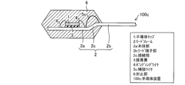
ただし、本実施形態にこける補強ワイヤの取り付け位置はこれに限るものではない。例えば、図4に示す半導体装置100cのように、補強ワイヤ5bに代えて、一端側がリードフレーム2のリード端子部2bの一部(封止部6によって被覆される部分)に取り付けられ、他端側がリードフレーム2の本体部2aにおける半導体チップ1が搭載されている領域よりもリード端子部2b側に取り付けられた補強ワイヤ5cを用いてもよい。
この場合、本体部2aにおける半導体チップ1よりも先端側の領域に取り付けられた補強ワイヤ5bを用いる場合に比べて、補強ワイヤ5cが半導体チップ1やボンディングワイヤ4などの他のワイヤと干渉することを容易に避けることができる。
このように、補強ワイヤの取り付け位置は、半導体装置の構造や特性等に応じてより最適な位置を選択すればよい。
なお、上述した補強ワイヤ5b,5cの両方を備えている構成としてもよい。また、補強ワイヤ5bおよび/または5cに加えて、実施形態1に示した補強ワイヤ5aを備えている構成としてもよい。
〔実施形態3〕
本発明のさらに他の実施形態について説明する。なお、説明の便宜上、上述した実施形態と同様の機能を有する部材については当該実施形態と同じ符号を付し、その説明を省略する。
本発明のさらに他の実施形態について説明する。なお、説明の便宜上、上述した実施形態と同様の機能を有する部材については当該実施形態と同じ符号を付し、その説明を省略する。
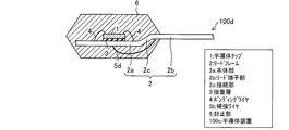
図5は、本実施形態にかかる半導体装置100dの断面図である。実施形態2に示した半導体装置100b,100cと異なる点は、補強ワイヤ5b,5cに代えて補強ワイヤ5dを備えている点である。
実施形態2では、一端側がリードフレーム2のリード端子部2bの一部に取り付けられ、他端側がリードフレーム2の本体部2aにおける表面側(半導体チップ1が搭載されている側)に取り付けられた補強ワイヤ5b,5cを用いていた。
これに対して、本実施形態では、図5に示したように、一端側がリードフレーム2のリード端子部2bの一部(封止部6によって被覆される部分)に取り付けられ、他端側がリードフレーム2の本体部2aにおける裏面側(半導体チップ1が搭載されていない側)に取り付けられた補強ワイヤ5dを用いている。
これにより、本実施形態では、上述した各実施形態と同様、封止材の注入によってリードフレーム2が変形することを防止できる。
また、補強ワイヤ5dを本体部2aの裏側(半導体チップ1が搭載されていない側)に取り付けることにより、補強ワイヤ5dが半導体チップ1やボンディングワイヤ4などの他の部材と干渉することを容易に避けることができる。
なお、図5に示した例では、半導体チップ1が本体部2aの表面側にのみ搭載されているが、これに限るものではなく、例えば、表面側および裏面側の両方に半導体チップ1が搭載されていてもよい。また、本体部2aの裏面側に半導体チップ1が搭載されている場合、補強ワイヤ5dの他端側の本体部2aに対する取り付け位置は、半導体チップ1が取り付けられている領域よりも先端側(リード端子部2bから遠い側)であってもよく、リード端子部2b側であってもよい。
また、補強ワイヤ5dに加えて、上述した補強ワイヤ5a,5b,5cのうちのいずれか1つ以上を備えている構成としてもよい。
〔実施形態4〕
本発明のさらに他の実施形態について説明する。なお、説明の便宜上、上述した実施形態と同様の機能を有する部材については当該実施形態と同じ符号を付し、その説明を省略する。
本発明のさらに他の実施形態について説明する。なお、説明の便宜上、上述した実施形態と同様の機能を有する部材については当該実施形態と同じ符号を付し、その説明を省略する。
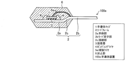
図6は、本実施形態にかかる半導体装置100eの断面図である。実施形態1に示した半導体装置100aと異なる点は、補強ワイヤ5aに代えて、2本の補強ワイヤ5e・5eを備えている点である。
実施形態1では、一端側がリードフレーム2のリード端子部2bに取り付けられ、他端側が半導体チップ1に取り付けられた補強ワイヤ5aを1本のみ用いていた。これに対して、本実施形態では、図6に示すように、一端側がリードフレーム2のリード端子部2bに取り付けられ、他端側が半導体チップ1に取り付けられた2本の補強ワイヤ5e・5eを用いている。
これにより、補強ワイヤを1本のみ用いる場合に比べて、リードフレーム2の変形を抑制する効果を高めることができる。また、補強ワイヤ5eとして比較的細いワイヤを用いる場合であっても、2本の補強ワイヤ5eを用いることによってリードフレーム2の変形を抑制する効果を高めることができる。
なお、図6に示した例では、2本の補強ワイヤ5e・5eを用いているが、補強ワイヤの本数はこれに限るものではなく、3本以上の補強ワイヤを用いてもよい。
また、図6に示した例では、各補強ワイヤ5eの他端側を半導体チップ1に取り付けているが、これに限らず、例えば、各補強ワイヤ5eの他端側を本体部2aの表面側に取り付けてもよく、本体部2aの裏面側に取り付けてもよい。
また、本実施形態では、半導体チップ1とリードフレーム2のリード端子部2bとに接続された補強ワイヤ5eを複数設ける構成について説明したが、これに限らず、補強ワイヤ5eに加えて、あるいは補強ワイヤ5eに代えて、1または複数本の補強ワイヤ5b、1または複数本の補強ワイヤ5c、および/または、1または複数本の補強ワイヤ5dを備える構成としてもよい。
〔実施形態5〕
本発明のさらに他の実施形態について説明する。なお、説明の便宜上、上述した実施形態と同様の機能を有する部材については当該実施形態と同じ符号を付し、その説明を省略する。
本発明のさらに他の実施形態について説明する。なお、説明の便宜上、上述した実施形態と同様の機能を有する部材については当該実施形態と同じ符号を付し、その説明を省略する。
図7は、本実施形態にかかる半導体装置100fの斜視図である。この図に示すように、半導体装置100fは、3つのリード端子部2b1,2b2,2b3を備えている。そして、リード端子部2b1,2b2にはリードフレーム2と半導体チップ1とを電気的に接続するためのボンディングワイヤ4が接続されており、リード端子部2b3には補強ワイヤ5fの一端側が取り付けられている。すなわち、本実施形態では、補強ワイヤ5fの一端側が、この補強ワイヤ5fに専用のリード端子部2b3に取り付けられている。なお、補強ワイヤ5fの他端側は半導体チップ1に取り付けられている。
このように、補強ワイヤ5fの一端側を専用のリード端子部2b3に接続する構成にすることにより、補強ワイヤ5fがボンディングワイヤ4等の他のワイヤと競合することを防止し、リードフレーム2の変形抑制効果(フレームフラット保持力)をより高めることができる。
なお、図7の例では、補強ワイヤ5fの他端側を半導体チップ1に取り付けているが、これに限るものではなく、例えば、リードフレーム2の本体部2aの表面あるいは裏面に取り付けてもよい。また、リード端子部2b3に複数本の補強ワイヤを取り付けるようにしてもよい。
また、本実施形態と上述したいずれかの実施形態とを組み合わせ、補強ワイヤ5fに加えて、補強ワイヤ5a~5eのうちのいずれか1つ以上を備える構成としてもよい。
〔まとめ〕
本発明の態様1にかかる半導体装置は、板状の本体部と上記本体部の一端側に接続されたリード端子部とを有するリードフレームと、上記本体部に搭載され、上記リードフレームに電気的に接続された半導体チップと、上記本体部と上記半導体チップと上記リード端子部の一部とを電気絶縁性を有する材料で被覆した封止部とを備えた半導体装置であって、一端側が上記リード端子部の上記一部に取り付けられ、他端側が上記本体部または上記本体部に搭載された部材に取り付けられた、上記リードフレームを補強する補強部材を備えていることを特徴としている。
本発明の態様1にかかる半導体装置は、板状の本体部と上記本体部の一端側に接続されたリード端子部とを有するリードフレームと、上記本体部に搭載され、上記リードフレームに電気的に接続された半導体チップと、上記本体部と上記半導体チップと上記リード端子部の一部とを電気絶縁性を有する材料で被覆した封止部とを備えた半導体装置であって、一端側が上記リード端子部の上記一部に取り付けられ、他端側が上記本体部または上記本体部に搭載された部材に取り付けられた、上記リードフレームを補強する補強部材を備えていることを特徴としている。
上記の構成によれば、補強部材を設けることにより、封止材の注入によってリードフレームの浮きあるいは反りが生じることを抑制できるので、リードフレーム上に形成される封止部の厚さを一定にすることができ、絶縁性の高い半導体装置を実現できる。また、従来の固定ピン方式におけるリードフレームにおける固定ピンに当接していた領域が封止材に被覆されずに露出してしまうという問題が生じることを防止できる。また、従来の可動ピン方式のように、可動ピンを移動させるための機構を設ける必要がないので、製造装置のコストアップを伴うことがない。したがって、絶縁性の高い半導体装置を容易かつ安価に実現することができる。また、リードフレーム上に形成される封止部の厚さを均一にすることができるので、リードフレームから封止部の外部への放熱性を向上させることができる。
本発明の態様2にかかる半導体装置は、上記態様1において、上記補強部材は、上記他端側が上記半導体チップに取り付けられている構成である。
上記の各構成によれば、絶縁性の高い半導体装置を容易かつ安価に実現することができる。
本発明の態様3にかかる半導体装置は、上記態様2において、上記補強部材は、導電性を有する材質からなり、上記半導体チップと上記リードフレームとの間の信号伝達のための信号線として機能する構成である。
上記の構成によれば、信号線と補強部材とを別々に設ける場合に比べて、部材数を減らすとともに半導体装置の構成を簡略化することができ、コストダウンを図ることができる。
本発明の態様4にかかる半導体装置は、上記態様1において、上記半導体チップは、上記本体部の一方の面に搭載されており、上記補強部材は、上記本体部における上記一方の面に取り付けられている構成である。
上記の各構成によれば、絶縁性の高い半導体装置を容易かつ安価に実現することができる。また、補強部材の他端側を半導体チップに取り付ける場合に比べて、半導体チップに負荷がかかることを防止できる。
本発明の態様5にかかる半導体装置は、上記態様1において、上記半導体チップは、上記本体部の一方の面に搭載されており、上記補強部材は、上記本体部の他方の面に取り付けられている構成である。
上記の各構成によれば、絶縁性の高い半導体装置を容易かつ安価に実現することができる。また、補強部材の他端側を半導体チップに取り付ける場合に比べて、半導体チップに負荷がかかることを防止できる。また、補強部材が、半導体チップとリードフレームとを接続するボンディングワイヤ等と干渉することを防止できる。
本発明の態様6にかかる半導体装置は、上記態様1~4のいずれかにおいて、上記補強部材は、複数本のワイヤ部材からなる構成である。
上記の構成によれば、複数のワイヤ部材を補強部材として用いることにより、リードフレームの浮きあるいは反り等を抑制する効果を高めることができる。
本発明の態様7にかかる半導体装置は、上記態様1~4のいずれかにおいて、複数の上記リード端子部を備えており、上記補強部材は、複数の上記リード端子部のうち上記封止部に被覆されて当該封止部の外部と電気的に絶縁されたダミー端子部に取り付けられている構成である。
上記の構成によれば、補強部材が半導体チップとリードフレームとを接続するボンディングワイヤ等と干渉することを防止できる。
本発明の一態様にかかる半導体装置の製造方法は、板状の本体部と上記本体部の一端側に接続されたリード端子部とを有するリードフレームと、上記本体部に搭載され、上記リードフレームに電気的に接続された半導体チップと、上記本体部と上記半導体チップと上記リード端子部の一部とを電気絶縁性を有する材料で被覆した封止部とを備えた半導体装置の製造方法であって、上記リードフレームを補強する補強部材の一端側を上記リード端子部の上記一部に取り付け、他端側を上記本体部または上記本体部に搭載された部材に取り付ける補強工程と、上記本体部、上記半導体チップ、上記リード端子部の一部、および上記補強部材を金型内の上記封止部を形成するための封止材が充填される充填空間に配置する配置工程と、上記充填空間に上記封止材を注入する注入工程とを含むことを特徴としている。
上記の方法によれば、補強部材を設けることにより、封止材の注入によってリードフレームの浮きあるいは反り等が生じることを抑制できるので、リードフレーム上に形成される封止部の厚さを一定にすることができ、絶縁性の高い半導体装置を実現できる。また、従来の固定ピン方式におけるリードフレームにおける固定ピンに当接していた領域が封止材に被覆されずに露出してしまうという問題が生じることを防止できる。また、従来の可動ピン方式のように、可動ピンを移動させるための機構を設ける必要がないので、製造装置のコストアップを伴うことがない。したがって、絶縁性の高い半導体装置を容易かつ安価に実現することができる。また、リードフレーム上に形成される封止部の厚さを均一にすることができるので、リードフレームから封止部の外部への放熱性を向上させることができる。
本発明は上述した各実施形態に限定されるものではなく、請求項に示した範囲で種々の変更が可能であり、異なる実施形態にそれぞれ開示された技術的手段を適宜組み合わせて得られる実施形態についても本発明の技術的範囲に含まれる。さらに、各実施形態にそれぞれ開示された技術的手段を組み合わせることにより、新しい技術的特徴を形成することができる。
本発明は、リードフレームを備えたフルモールドパッケージの半導体装置およびその製造方法に適用できる。
1 半導体チップ
2 リードフレーム
2a 本体部
2b,2b1,2b2 リード端子部
2b3 リード端子部(ダミー端子部)
2c 接続部
3 接着層
4 ボンディングワイヤ
5a~5f 補強ワイヤ
6 封止部
11 上金型
12 下金型
13 封止材注入口
14 充填空間
100a~100f 半導体装置
2 リードフレーム
2a 本体部
2b,2b1,2b2 リード端子部
2b3 リード端子部(ダミー端子部)
2c 接続部
3 接着層
4 ボンディングワイヤ
5a~5f 補強ワイヤ
6 封止部
11 上金型
12 下金型
13 封止材注入口
14 充填空間
100a~100f 半導体装置
Claims (6)
- 板状の本体部と上記本体部の一端側に接続されたリード端子部とを有するリードフレームと、
上記本体部に搭載され、上記リードフレームに電気的に接続された半導体チップと、
上記本体部と上記半導体チップと上記リード端子部の一部とを電気絶縁性を有する材料で被覆した封止部とを備えた半導体装置であって、
一端側が上記リード端子部の上記一部に取り付けられ、他端側が上記本体部または上記本体部に搭載された部材に取り付けられた、上記リードフレームを補強する補強部材を備えていることを特徴とする半導体装置。 - 上記補強部材は、上記他端側が上記半導体チップに取り付けられていることを特徴とする請求項1に記載の半導体装置。
- 上記補強部材は、導電性を有する材質からなり、上記半導体チップと上記リードフレームとの間の信号伝達のための信号線として機能することを特徴とする請求項2に記載の半導体装置。
- 上記半導体チップは、上記本体部の一方の面に搭載されており、
上記補強部材は、上記本体部における上記一方の面に取り付けられていることを特徴とする請求項1から3のいずれか1項に記載の半導体装置。 - 上記半導体チップは、上記本体部の一方の面に搭載されており、
上記補強部材は、上記本体部の他方の面に取り付けられていることを特徴とする請求項1から3のいずれか1項に記載の半導体装置。 - 板状の本体部と上記本体部の一端側に接続されたリード端子部とを有するリードフレームと、上記本体部に搭載され、上記リードフレームに電気的に接続された半導体チップと、上記本体部と上記半導体チップと上記リード端子部の一部とを電気絶縁性を有する材料で被覆した封止部とを備えた半導体装置の製造方法であって、
上記リードフレームを補強する補強部材の一端側を上記リード端子部の上記一部に取り付け、他端側を上記本体部または上記本体部に搭載された部材に取り付ける補強工程と、
上記本体部、上記半導体チップ、上記リード端子部の一部、および上記補強部材を金型内の上記封止部を形成するための封止材が充填される充填空間に配置する配置工程と、
上記充填空間に上記封止材を注入する注入工程とを含むことを特徴とする半導体装置の製造方法。
Applications Claiming Priority (2)
| Application Number | Priority Date | Filing Date | Title |
|---|---|---|---|
| JP2013094720 | 2013-04-26 | ||
| JP2013-094720 | 2013-04-26 |
Publications (1)
| Publication Number | Publication Date |
|---|---|
| WO2014174873A1 true WO2014174873A1 (ja) | 2014-10-30 |
Family
ID=51791458
Family Applications (1)
| Application Number | Title | Priority Date | Filing Date |
|---|---|---|---|
| PCT/JP2014/052876 Ceased WO2014174873A1 (ja) | 2013-04-26 | 2014-02-07 | 半導体装置およびその製造方法 |
Country Status (1)
| Country | Link |
|---|---|
| WO (1) | WO2014174873A1 (ja) |
Citations (2)
| Publication number | Priority date | Publication date | Assignee | Title |
|---|---|---|---|---|
| JP2001068586A (ja) * | 1999-08-25 | 2001-03-16 | Fujitsu Ltd | 半導体装置 |
| JP2010040613A (ja) * | 2008-07-31 | 2010-02-18 | Nichia Corp | 発光装置 |
-
2014
- 2014-02-07 WO PCT/JP2014/052876 patent/WO2014174873A1/ja not_active Ceased
Patent Citations (2)
| Publication number | Priority date | Publication date | Assignee | Title |
|---|---|---|---|---|
| JP2001068586A (ja) * | 1999-08-25 | 2001-03-16 | Fujitsu Ltd | 半導体装置 |
| JP2010040613A (ja) * | 2008-07-31 | 2010-02-18 | Nichia Corp | 発光装置 |
Similar Documents
| Publication | Publication Date | Title |
|---|---|---|
| JP5873998B2 (ja) | 半導体装置及びその製造方法 | |
| US7714455B2 (en) | Semiconductor packages and methods of fabricating the same | |
| CN102820288B (zh) | 功率模块及其制造方法 | |
| US20140264801A1 (en) | Semiconductor device | |
| US20130154068A1 (en) | Packaged leadless semiconductor device | |
| US8633511B2 (en) | Method of producing semiconductor device packaging having chips attached to islands separately and covered by encapsulation material | |
| JP2014072305A (ja) | 半導体モジュールの製造方法、接合装置、半導体モジュール | |
| JP2017135230A (ja) | 半導体装置およびその製造方法 | |
| JP2009289920A (ja) | 半導体装置の製造方法 | |
| JP5983249B2 (ja) | 半導体モジュールの製造方法 | |
| CN102751205A (zh) | 半导体器件及其制造方法 | |
| CN102348332A (zh) | 电路装置及其制造方法 | |
| CN106463417A (zh) | 半导体装置的制造方法 | |
| CN1672260A (zh) | 可表面安装的半导体器件及其制造方法 | |
| CN104795337A (zh) | 电力用半导体装置及其制造方法 | |
| US20140117525A1 (en) | Power module package and method of manufacturing the same | |
| CN203367261U (zh) | 功率模块 | |
| JP2005116937A (ja) | 半導体発光装置およびその製造方法 | |
| CN103855275A (zh) | Led封装支架模组及其单体、led封装结构 | |
| WO2014174873A1 (ja) | 半導体装置およびその製造方法 | |
| CN220753419U (zh) | 集成电路封装件 | |
| US20230275008A1 (en) | Semiconductor package with overlapping leads and die pad | |
| JP5377733B2 (ja) | 電力用半導体装置 | |
| JP6104545B2 (ja) | 半導体装置の製造方法、および成形部材 | |
| US7821141B2 (en) | Semiconductor device |
Legal Events
| Date | Code | Title | Description |
|---|---|---|---|
| 121 | Ep: the epo has been informed by wipo that ep was designated in this application |
Ref document number: 14787769 Country of ref document: EP Kind code of ref document: A1 |
|
| NENP | Non-entry into the national phase |
Ref country code: DE |
|
| 122 | Ep: pct application non-entry in european phase |
Ref document number: 14787769 Country of ref document: EP Kind code of ref document: A1 |
|
| NENP | Non-entry into the national phase |
Ref country code: JP |